ADC1038
10-Bit Serial I/O A/D Converter with Analog Multiplexer
and Track/Hold Function
General Description
TheADC1038 is a 10-bit successive approximation A/D converters with serial I/O. The serial input controls a
single-ended analog multiplexer that selects one of 8 input
channels. The serial output data can be configured into a
left- or right-justified format.
An input track/hold is implemented by a capacitive reference
ladder and sampled-data comparator.This allows the analog
input to vary during the A/D conversion cycle.
Separate serial I/O and conversion clock inputs are provided
to facilitate the interface to various microprocessors.
Applications
n Engine control
n Process control
n Instrumentation
n Test equipment
Features
n Serial I/O ( MICROWIRE™compatible)
n Separate asynchronous converter clock and serial data
I/O clock
n Analog input track/hold function
n Ratiometric or absolute voltage referencing
n No zero or full scale adjustment required
n 0V to 5V analog input range with single 5V power
supply
n TTL/MOS input/output compatible
n No missing codes
Key Specifications
n Resolution 10 bit
n Total unadjusted error
±
1 LSB (max)
n Single supply 5V
±
5
%
n Power dissipation 20 mW (max)
n Max. conversion time (f
C
=
3 MHz) 13.7 µs (max)
n Serial data exchange time (f
S
=
1 MHz) 10 µs (max)
Connection Diagrams
Ordering Information
Industrial −40˚C ≤ TA≤ +85˚C Package
ADC1038CIWM M20B
TRI-STATE®is a registered trademark of National Semiconductor Corporation.
MICROWIRE
™
is a trademark of National Semiconductor Corporation.
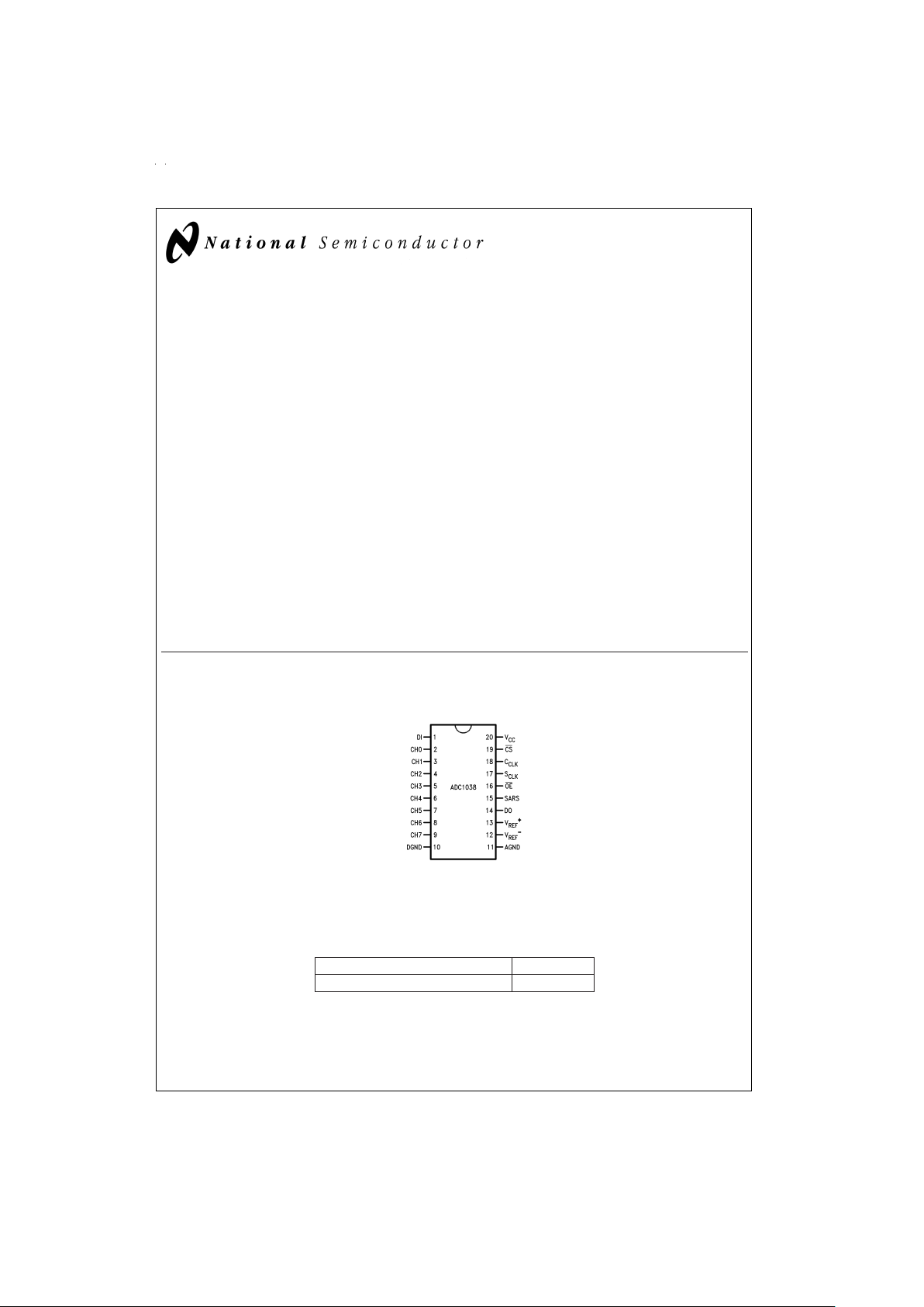
SO Package
DS010556-2
Top View
ADC1038 In NS Package
M20B
June 1999
ADC1038 10-Bit Serial I/O A/D Converter with Analog Multiplexer and Track/Hold Function
© 1999 National Semiconductor Corporation DS010556 www.national.com

Absolute Maximum Ratings (Notes 1, 3)
If Military/Aerospace specified devices are required,
please contact the National Semiconductor Sales Office/
Distributors for availability and specifications.
Supply Voltage (V
CC
) 6.5V
Voltage at Inputs and Outputs −0.3V to V
CC
+ 0.3V
Input Current at Any Pin (Note 4)
±
5mA
Package Input Current (Note 4)
±
20 mA
Package Dissipation
at T
A
=
25˚C (Note 5) 500 mW
ESD Susceptability (Note 6) 2000V
Soldering Information
SO Package (Note 7) :
Vapor Phase (60 sec.) 215˚C
Infrared (15 sec.) 220˚C
Storage Temperature −65˚C to +150˚C
Operating Ratings (Notes 2, 3)
Temperature Range T
MIN
≤ TA≤ T
MAX
ADC1038CIWM −40˚C ≤ TA≤ +85˚C
Supply Voltage (V
CC
) 4.75 VDCto 5.25 V
DC
Reference Voltage
(V
REF
=
V
REF
+
−V
REF
−
) 2.0 VDCto VCC+ 0.05V
Electrical Characteristics
The following specifications apply for V
CC
=
+5.0V, V
REF
=
+4.6V, f
S
=
700 kHz, and f
C
=
3 MHz unless otherwise specified.
Boldface limits apply for T
A
=
T
J
=
T
MIN
to T
MAX
; all other limits T
A
=
T
J
=
25˚C.
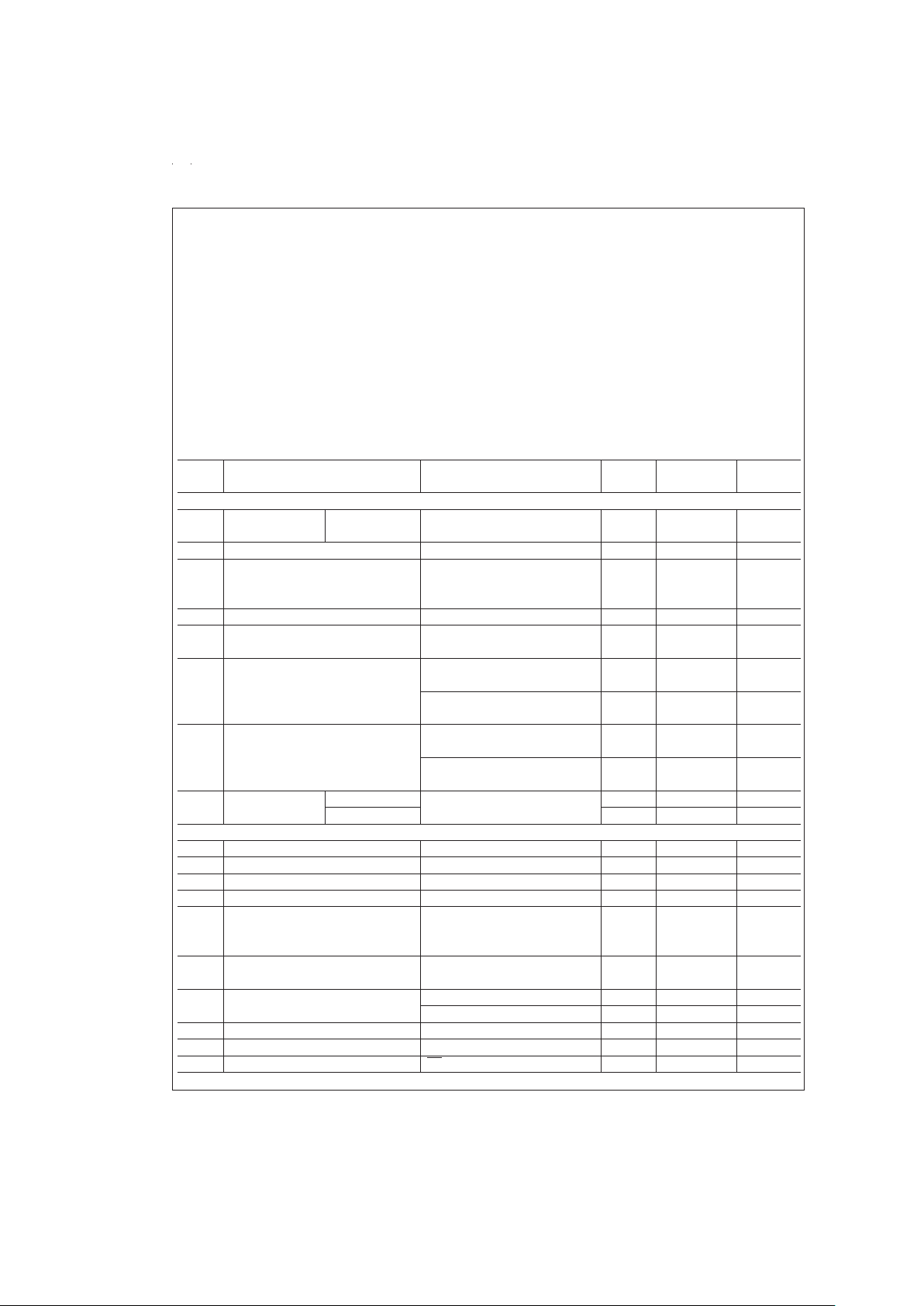
Symbol Parameter Conditions Typical Limit Units
(Note 8) (Note 9) (Limits)
CONVERTER AND MULTIPLEXER CHARACTERISTICS
Total Unadjusted CIN, CIWM, CMJ (Note 10)
±
1 LSB (max)
Error
Differential Linearity 10 Bits (min)
R
REF
Reference Input Resistance 8 kΩ
5 kΩ (min)
11 kΩ (max)
V
REF
Reference Voltage (VCC+ 0.05) V (max)
V
IN
Analog Input Voltage (Note 11) (VCC+ 0.05) V (max)
(GND − 0.05) V (min)
On Channel Leakage Current On Channel=5V
DC
, 5.0 200 nA (max)
Off Channel=0V
DC
500 nA (max)
(Note 12) On Channel=0V
DC
, 5.0 −200 nA (max)
Off Channel=5V
DC
−500 nA (max)
Off Channel Leakage Current On Channel=5V
DC
, 5.0 −200 nA (max)
Off Channel=0V
DC
−500 nA (max)
(Note 12) On Channel=0V
DC
, 5.0 200 nA (max)
Off Channel=5V
DC
500 nA (max)
Power Supply Zero Error 4.75 V
DC
≤ VCC≤ 5.25 V
DC
±
1/4 LSB (max)
Sensitivity Full Scale Error
±
1/4 LSB (max)
DIGITAL AND DC CHARACTERISTICS
V
IN(1)
Logical “1” Input Voltage V
CC
=
5.25 V
DC
2.0 V (min)
V
IN(0)
Logical “0” Input Voltage V
CC
=
4.75 V
DC
0.8 V (max)
I
IN(1)
Logical “1” Input Current V
IN
=
5.0 V
DC
0.005 2.5 µA (max)
I
IN(0)
Logical “0” Input Current V
IN
=
0V
DC
−0.005 −2.5 µA (max)
V
OUT(1)
Logical “1” Output Voltage V
CC
=
4.75 V
DC
I
OUT
=
−360 µA 2.4 V (min)
I
OUT
=
−10 µA 4.5 V (min)
V
OUT(0)
Logical “0” Output Voltage V
CC
=
4.75 V
DC
0.4 V (max)
I
OUT
=
1.6 mA
I
OUT
TRI-STATE Output Current V
OUT
=
0V −0.01 −3 µA (max)
V
OUT
=
5V 0.01 3 µA (max)
I
SOURCE
Output Source Current V
OUT
=
0V −14 −6.5 mA (min)
I
SINK
Output Sink Current V
OUT
=
V
CC
16 8.0 mA (min)
I
CC
Supply Current CS=HIGH, V
REF
Open 1.5 3 mA (max)
www.national.com 2

Electrical Characteristics (Continued)
The following specifications apply for V
CC
=
+5.0V, V
REF
=
+4.6V, f
S
=
700 kHz, and f
C
=
3 MHz unless otherwise specified.
Boldface limits apply for T
A
=
T
J
=
T
MIN
to T
MAX
; all other limits T
A
=
T
J
=
25˚C.
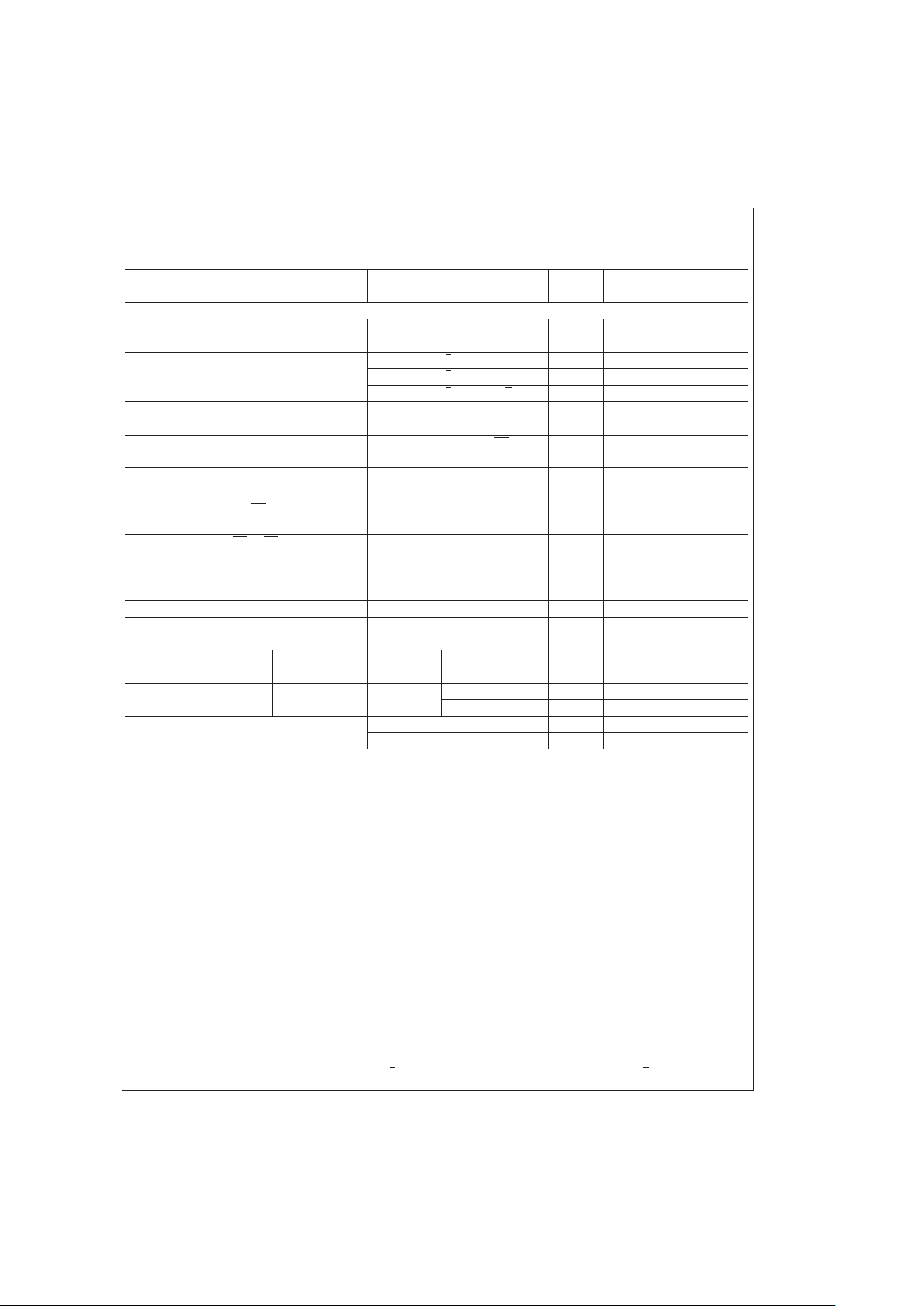
Symbol Parameter Conditions Typical Limit Units
(Note 8) (Note 9) (Limits)
AC CHARACTERISTICS
f
C
Conversion Clock (C
CLK
) 0.7 MHz (min)
Frequency 4.0 3.0 MHz (max)
f
S
Serial Data Clock (S
CLK
)f
C
=
3 MHz, R/L=“0”
183 kHz (min)
Frequency (Note 13) f
C
=
3 MHz, R/L=“1”
622 kHz (min)
f
C
=
3 MHz, R/L=“0” or R/L=“1”
2 1.0 MHz (max)
T
C
Conversion Time Not Including MUX Addressing and 41 (1/fC) (max)
Analog Input Sampling Times + 200 ns
t
CA
Analog Sampling Time After Address is Latched,CS=Low 4.5 (1/fS) (max)
+ 200 ns
t
ACC
Access Time Delay from CS or OE OE=“0” 100 200 ns (max)
Falling Edge to DO Data Valid
t
SET-UP
Set-up Time of CS Falling 75 150 ns (min)
Edge to S
CLK
Rising Edge
t
1H,t0H
Delay from OE or CS Rising R
L
=
3kΩ,C
L
=
100 pF 100 120 ns (max)
Edge to DO TRI-STATE
t
HDI
DI Hold Time from S
CLK
Rising Edge 0 50 ns (min)
t
SDI
DI Set-up Time to S
CLK
Rising Edge 50 100 ns (min)
t
HDO
DO Hold Time from S
CLK
Falling Edge R
L
=
30 kΩ,C
L
=
100 pF 70 10 ns (min)
t
DDO
Delay from S
CLK
Falling R
L
=
30 kΩ,C
L
=
100 pF 150 250 ns (max)
Edge to DO Data Valid
t
RDO
DO Rise Time R
L
=
30 kΩ, TRI-STATE to High 35 75 ns (max)
C
L
=
100 pF Low to High 75 150 ns (max)
t
FDO
DO Fall Time R
L
=
30 kΩ, TRI-STATE to Low 35 75 ns (max)
C
L
=
100 pF High to Low 75 150 ns (max)
C
IN
Input Capacitance Analog Inputs (CH0–CH7) 50 pF
All Other Inputs 7.5 pF
Note 1: Absolute Maximum Ratings indicate limits beyond which damage to the device may occur.
Note 2: Operating Ratings indicate conditions for which the device is functional, but do not guarantee specific performance limits. For guaranteed specifications and
test conditions, see the Electrical Characteristics. The guaranteed specifications apply only for the test conditions listed. Some performance characteristics may degrade when the device is not operated under the listed test conditions.
Note 3: All voltages are measured with respect to AGND and DGND, unless otherwise specified.
Note 4: When the input voltage (V
IN
) at any pin exceeds the power supplies (V
IN
<
DGND, or V
IN
>
VCC) the current at that pin should be limited to 5 mA. The 20 mA
maximum package input current rating limits the number of pins that can safely exceed the power supplies with an input current of 5 mA to four pins.
Note 5: The maximum power dissipation must be derated at elevated temperatures and is dictated by T
Jmax
, θJAand the ambient temperature, TA. The maximum
allowable power dissipation at any temperature is P
D
=
(T
Jmax−TA
)/θJAor the number given in the Absolute Maximum Ratings, whichever is lower. For this device,
T
Jmax
=
125˚C. The typical thermal resistance (θ
JA
) when board mounted is 64˚C/W.
Note 6: Human body model, 100 pF capacitor discharged through a 1.5 kΩ resistor.
Note 7: See AN450 “Surface Mounting Methods and Their Effect on Product Reliability” or Linear Databook section “Surface Mount” for other methods of soldering
surface mount devices.
Note 8: Typicals are at T
J
=
25˚C and represent most likely parametric norm.
Note 9: Limits are guaranteed to National’s AOQL (Average Outgoing Quality Level).
Note 10: Total unadjusted error includes offset, full-scale, linearity, multiplexer, and hold step errors.
Note 11: Two on-chip diodes are tied to each analog input. They will forward-conduct for analog input voltages one diode drop below ground or one diode drop
greater than V
CC
supply. Be careful during testing at low VCClevels (4.5V), as high level analog inputs (5V) can cause an input diode to conduct, especially at elevated temperatures, which will cause errors for analog inputs near full-scale. The spec allows 50 mV forward bias of either diode; this means that as long as the
analog V
IN
does not exceed the supply voltage by more than 50 mV,the output code will be correct. Exceeding this range on an unselected channel will corrupt the
reading of a selected channel. Toachieve an absolute 0 V
DC
to 5 VDCinput voltage range will therefore require a minimum supply voltage of 4.950 VDCover tem-
perature variations, initial tolerance and loading.
Note 12: Channel leakage current is measured after the channel selection.
Note 13: In order to synchronize the serial data exchange properly, SARS needs to go low after completion of the serial I/O data exchange. If this does not occur
the output shift register will be reset and the correct output data lost. The minimum limit for S
CLK
will depend on C
CLK
frequency and whether right-justified or
left-justified, and can be determined by the following equations:
f
S
>
(8.5/41) (fC) with right-justification (R/L=“1”) and f
S
>
(2.5/41) (fC) with left-justification (R/L=“0”).
www.national.com3

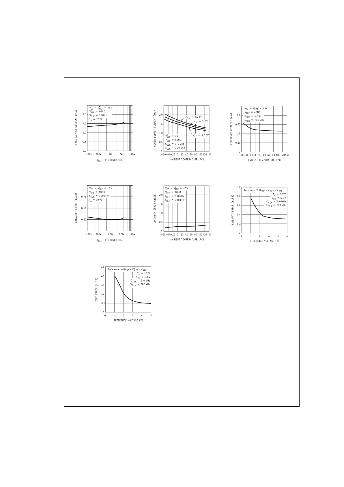
Typical Performance Characteristics
Power Supply Current
(I
CC
)vsC
CLK
DS010556-28
Power Supply Current (ICC)
vs Ambient Temperature
DS010556-29
Reference Current (I
REF
)
vs Ambient Temperature
DS010556-30
Linearity Error vs
C
CLK
Frequency
DS010556-31
Linearity Error vs
Ambient Temperature
DS010556-32
Linearity Error vs
Reference Voltage
DS010556-33
Zero Error vs
Reference Voltage
DS010556-34
www.national.com 4
 Loading...