NSC 5962-9219001MSA, 5962-9219001MRA, 5962-9219001M2A Datasheet

54ACTQ377
Octal D Flip-Flop with Clock Enable
General Description
The ACTQ377 has eight edge-triggered, D-type flip-flops
with individual D inputs and Q outputs. The common buffered Clock (CP) input loads all flip-flops simultaneously,
when the Clock Enable (CE) is LOW.
The register is fully edge-triggered. The state of each D input, one setup time before the LOW-to-HIGH clock transition, is transferred to the corresponding flip-flop’s Q output.
The CE input must be stable only one setup time prior to the
LOW-to-HIGH clock transition for predictable operation.
The ACTQ377 utilizes FACT Quiet Series
®
technology to
guarantee quiet output switching and improved dynamic
threshold performance. FACT Quiet Series features GTO
®
output control and undershoot corrector in addition to a split
ground bus for superior performance.
Features
n Ideal for addressable register applications
n Clock enable for address and data synchronization
applications
n Eight edge-triggered D flip-flops
n Buffered common clock
n Outputs source/sink 24 mA
n See ’273 for master reset version
n See ’373 for transparent latch version
n See ’374 for TRI-STATE
®
version
n Guaranteed simultaneous switching noise level and
dynamic threshold performance
n TTL-compatible inputs and outputs
n Standard Microcircuit Drawing (SMD) 5962-9219001
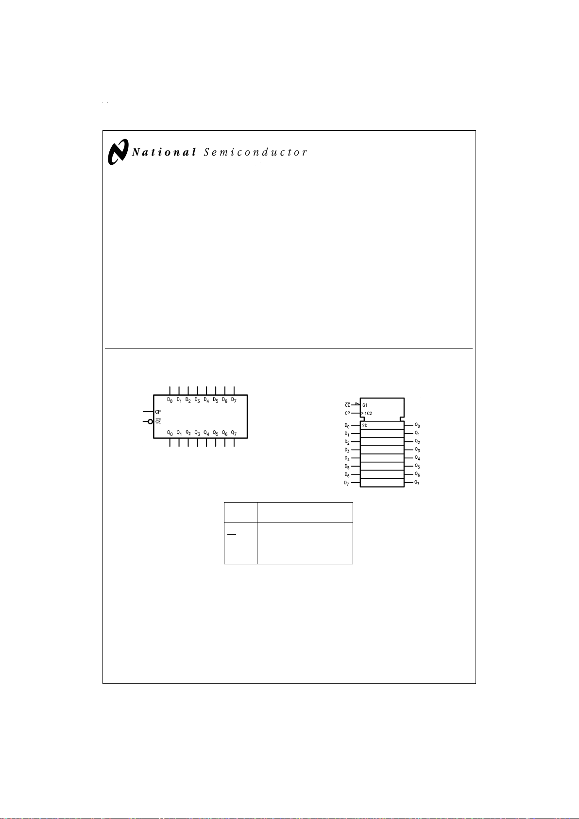
Logic Symbols
Pin
Names
Description
D
0–D7
Data Inputs
CE
Clock Enable (Active LOW)
Q
0–Q7
Data Outputs
CP Clock Pulse Input
GTO®is a trademark of National Semiconductor Corporation.
TRI-STATE
®
is a registered trademark of National Semiconductor Corporation.
FACT
®
and FACT Quiet Series®are registered trademarks of Fairchild Semiconductor Corporation.
DS100357-1
IEEE/IEC
DS100357-2
September 1998
54ACTQ377 Octal D Flip-Flop with Clock Enable
© 1998 National Semiconductor Corporation DS100357 www.national.com

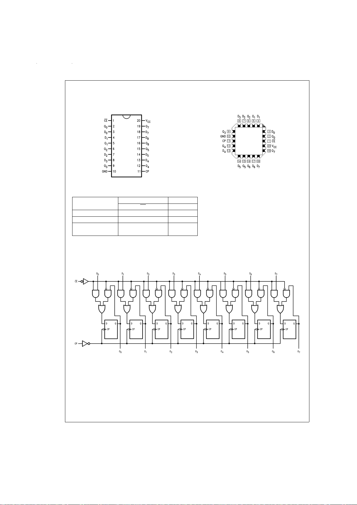
Connection Diagrams
Mode Select-Function Table
Operating Mode Inputs Outputs
CP CE
D
n
Q
n
Load ‘1’ N L H H
Load ‘0’ N L L L
Hold (Do Nothing) N H X No Change
X H X No Change
H=HIGH Voltage Level
L=LOW Voltage Level
X=Immaterial
N=LOW-to-HIGH Clock Transition
Logic Diagram
Pin Assignment
for DIP and Flatpak
DS100357-3
Pin Assignment
for LCC
DS100357-4
DS100357-5
Please note that this diagram is provided only for the understanding of logic operations and should not be used to estimate propagation delays.
www.national.com 2
 Loading...