NSC 5962-9059301MEA, 5962-9059301M2A Datasheet

TL/F/9535
54F/74F402 Serial Data Polynomial Generator/Checker
January 1995
54F/74F402 Serial Data Polynomial
Generator/Checker
General Description
The ’F402 expandable Serial Data Polynomial generator/
checker is an expandable version of the ’F401. It provides
an advanced tool for the implementation of the most widely
used error detection scheme in serial digital handling systems. A 4-bit control input selects one-of-six generator polynomials. The list of polynomials includes CRC-16, CRCCCITT and Ethernet
É
, as well as three other standard poly-
nomials (56
th
order, 48thorder, 32ndorder). Individual clear
and preset inputs are provided for floppy disk and other
applications. The Error output indicates whether or not a
transmission error has occurred. The CWG Control input
inhibits feedback during check word transmission. The
’F402 is compatible with FAST
É
devices and with all TTL
families.
Features
Y
Guaranteed 30 MHz data rate
Y
Six selectable polynomials
Y
Other polynomials available
Y
Separate preset and clear controls
Y
Expandable
Y
Automatic right justification
Y
Error output open collector
Y
Typical applications:
Floppy and other disk storage systems
Digital cassette and cartridge systems
Data communication systems
Commercial Military
Package
Package Description
Number
74F402PC N16E 16-Lead (0.300×Wide) Molded Dual-In-Line
54F402DM (Note 1) J16A 16-Lead Ceramic Dual-In-Line
54F402FM (Note 1) W16A 16-Lead Cerpack
54F402LM (Note 1) E20A 20-Lead Ceramic Leadless Chip Carrier, Type C
Note 1: Military grade device with environmental and burn-in processing. Use suffixeDMQB, FMQB and LMQB.
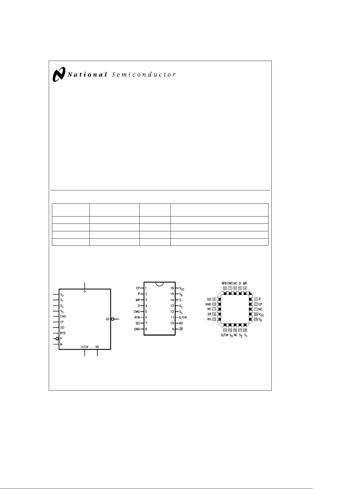
Logic Symbol Connection Diagrams
TL/F/9535– 4
Pin Assignment
for DIP, SOIC and Flatpak
TL/F/9535– 1
Pin Assignment
for LCC
TL/F/9535– 2
TRI-STATEÉis a registered trademark of National Semiconductor Corporation.
Ethernet
É
is a registered trademark of Xerox Corporation.
C
1995 National Semiconductor Corporation RRD-B30M105/Printed in U. S. A.

Unit Loading/Fan Out
54F/74F
Pin Names Description
U.L. Input I
IH/IIL
HIGH/LOW Output IOH/I
OL
S0–S
3
Polynomial Select Inputs 1.0/0.67 20 mA/b0.4 mA
CWG Check Word Generate Input 1.0/0.67 20 mA/
b
0.4 mA
D/CW Serial Data/Check Word 285(100)/13.3(6.7)
b
5.7 mA(b2 mA)/8 mA (4 mA)
D Data Input 1.0/0.67 20 mA/b0.4 mA
ER
Error Output */26.7(13.3) */16 mA (8 mA)
RO Register Output 285(100)/13.3(6.7)
b
5.7 mA(b2 mA)/8 mA (4 mA)
CP Clock Pulse 1.0/0.67 20 mA/
b
0.4 mA
SEI Serial Expansion Input 1.0/0.67 20 mA/
b
0.4 mA
RFB Register Feedback 1.0/0.67 20 mA/
b
0.4 mA
MR Master Reset 1.0/0.67 20 mA/
b
0.4 mA
P
Preset 1.0/0.67 20 mA/b0.4 mA
*Open Collector
Functional Description
The ’F402 Serial Data Polynomial Generator/Checker is an
expandable 16-bit programmable device which operates on
serial data streams and provides a means of detecting
transmission errors. Cyclic encoding and decoding schemes
for error detection are based on polynomial manipulation in
modulo arithmetic. For encoding, the data stream (message
polynomial) is divided by a selected polynomial. This division results in a remainder (or residue) which is appended to
the message as check bits. For error checking, the bit
stream containing both data and check bits is divided by the
same selected polynomial. If there are no detectable errors,
this division results in a zero remainder. Although it is possible to choose many generating polynomials of a given degree, standards exist that specify a small number of useful
polynomials. The ’F402 implements the polynomials listed in
Table I by applying the appropriate logic levels to the select
pins S
0,S1,S2
and S3.
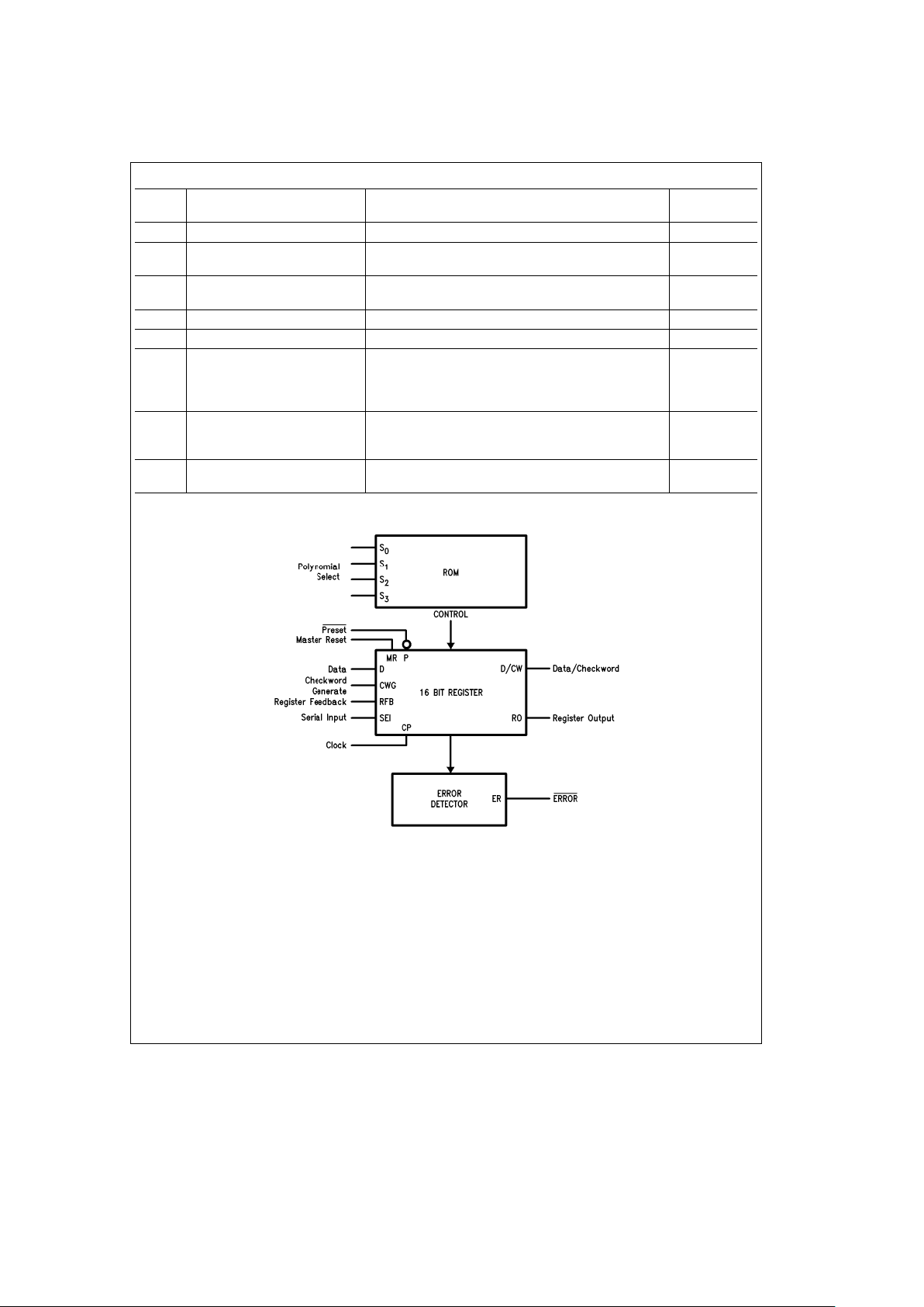
The ’F402 consists of a 16-bit register, a Read Only Memory
(ROM) and associated control circuitry as shown in the
Block Diagram. The polynomial control code presented at
inputs S
0,S1,S2
and S3is decoded by the ROM, selecting
the desired polynomial or part of a polynomial by establishing shift mode operation on the register with Exclusive OR
(XOR) gates at appropriate inputs. To generate the check
bits, the data stream is entered via the Data Inputs (D), using the LOW-to-HIGH transition of the Clock Input (CP). This
data is gated with the most significant Register Output (RO)
via the Register Feedback Input (RFB), and controls the
XOR gates. The Check Word Generate (CWG) must be held
HIGH while the data is being entered. After the last data bit
is entered, the CWG is brought LOW and the check bits are
shifted out of the register(s) and appended to the data bits
(no external gating is needed).
To check an incoming message for errors, both the data
and check bits are entered through the D Input with the
CWG Input held HIGH. The Error Output becomes valid after the last check bit has been entered into the ’F402 by a
LOW-to-HIGH transition of CP, with the exception of the
Ethernet polynomial (see Applications paragraph). If no detectable errors have occurred during the data transmission,
the resultant internal register bits are all LOW and the Error
Output (ER
) is HIGH. If a detectable error has occurred, ER
is LOW. ER remains valid until the next LOW-to-HIGH transition of CP or until the device has been preset or reset.
A HIGH on the Master Reset Input (MR) asynchronously
clears the entire register. A LOW on the Preset Input (P
)
asynchronously sets the entire register with the exception
of:
1 The Ethernet residue selection, in which the registers
containing the non-zero residue are cleared;
2 The 56th order polynomial, in which the 8 least significant
register bits of the least significant device are cleared;
and,
3 Register S
e
0, in which all bits are cleared.
2

TABLE I
Hex
Select Code
Polynomial Remarks
S
3
S
2
S
1
S
0
0 LLLL0 S
e
0
CHHLLX
32
a
X
26
a
X
23
a
X
22
a
X
16
a
Ethernet
D HHLHX
12
a
X
11
a
X
10
a
X
8
a
X
7
a
X
5
a
X
4
a
X
2
aXa
1 Polynomial
E HHH LX
32
a
X
31
a
X
27
a
X
26
a
X
25
a
X
19
a
X
16
a
Ethernet
F HHHHX
15
a
X
13
a
X
12
a
X
11
a
X
9
a
X
7
a
X
6
a
X
5
a
X
4
a
X
2
aXa
1 Residue
7 L HHHX
16
a
X
15
a
X
2
a
1 CRC-16
B HLHHX
16
a
X
12
a
X
5
a
1 CRC-CCITT
3LLHHX
56
a
X
55
a
X
49
a
X
45
a
X
41
a
2 L LHLX
39
a
X
38
a
X
37
a
X
36
a
X
31
a
56th
4 LHL LX
22
a
X
19
a
X
17
a
X
16
a
X
15
a
X
14
a
X
12
a
X
11
a
X
9
a
Order
8 HLLLX
5
a
X
a
1
5 LHLHX
48
a
X
36
a
X
35
a
9HLLHX
23
a
X
21
a
48th
1 LLLHX
15
a
X
13
a
X
8
a
X
2
a
1
Order
6LHHLX
32
a
X
23
a
X
21
a
32nd
A HLHLX
11
a
X
2
a
1 Order
Block Diagram
TL/F/9535– 5
3

TABLE II
Select Code P
3
P
2
P
1
P
0
C
2
C
1
C
0
Polynomial
0 0000100S
e
0
C 1 1 1 1 1 0 1 Ethernet
D 1 1 1 1 1 0 1 Polynomial
E 0 0 0 0 0 0 0 Ethernet
F 0 0 0 0 0 1 0 Residue
7 1 1 1 1 1 0 0 CRC-16
B 1 1 1 1 1 0 0 CRC-CCITT
3 1111100
2 1 1 1 1 1 0 0 56th
4 1 1 1 1 1 0 0 Order
8 0011100
5 1111100
48th
9 1111100
Order
1 1111100
6 1 1 1 1 1 0 0 32nd
A 1 1 1 1 1 0 0 Order
Applications
In addition to polynomial selection there are four other capabilities provided for in the ’F402 ROM. The first is set or
clear selectability. The sixteen internal registers have the
capability to be either set or cleared when P
is brought
LOW. This set or clear capability is done in four groups of 4
(see Table II, P
0–P3
). The second ROM capability (C0)isin
determining the polarity of the check word. As is the case
with the Ethernet polynomial the check word can be inverted when it is appended to the data stream or as is the case
with the other polynomials, the residue is appended with no
inversion. Thirdly, the ROM contains a bit (C
1
) which is used
to select the RFB input instead of the SEI input to be fed
into the LSB. This is used when the polynomial selected is
actually a residue (least significant) stored in the ROM
which indicates whether the selected location is a polynomial or a residue. If the latter, then it inhibits the RFB input.
As mentioned previously, upon a successful data transmission, the CRC register has a zero residue. There is an exception to this, however, with respect to the Ethernet polynomial. This polynomial, upon a successful data transmission, has a non-zero residue in the CRC register (C7 04 DD
7B)
16
. In order to provide a no-error indication, two ROM
locations have been preloaded with the residue so that by
selecting these locations and clocking the device one additional time, after the last check bit has been entered, will
result in zeroing the CRC register. In this manner a no-error
indication is achieved.
With the present mix of polynomials, the largest is 56
th
or-
der requiring four devices while the smallest is 16
th
order
requiring just one device. In order to accommodate multiplexing between high order polynomials (X 16
th
order) and
lower order polynomials, a location of all zeros is provided.
This allows the user to choose a lower order polynomial
even if the system is configured for a higher order one.
The ’F402 expandable CRC generator checker contains 6
popular CRC polynomials, 2-16
th
Order, 2-32ndOrder, 1-
48
th
Order and 1-56thOrder. The application diagram
shows the ’F402 connected for a 56
th
Order polynomial.
Also shown are the input patterns for other polynomials.
When the ’F402 is used with a gated clock, disabling the
clock in a HIGH state will ensure no erroneous clocking
occurs when the clock is re-enabled. Preset and Master Reset are asynchronous inputs presetting the register to S or
clearing to 1s respectively (note Ethernet residue and 56
th
Order select code 8, LSB, are exceptions to this).
To generate a CRC, the pattern for the selected polynomial
is applied to the S inputs, the register is preset or cleared as
required, clock is enabled, CWG is set HIGH, data is applied
to D input, output data is on D/CW. When the last data bit
has been entered, CWG is set LOW and the register is
clocked for n bits (where n is the order of the polynomial).
The clock may now be stopped if desired (holding CWG
LOW and clocking the register will output zeros from D/CW
after the residue has been shifted out).
To check a CRC, the pattern for the selected polynomial is
applied to the S inputs, the register is preset or cleared as
required, clock is enabled, CWG is set HIGH, the data
stream including the CRC is applied to D input. When the
last bit of the CRC has been entered, the ER
output is
checked: HIGH
e
error free data, LOWecorrupt data. The
clock may now be stopped if desired.
To implement polynomials of lower order than 56
th
, select
the number of packages required for the order of polynomial
and apply the pattern for the selected polynomial to the S
inputs (0000 on S inputs disables the package from the
feedback chain).
4
 Loading...