NSC 5962-8965801SA, 5962-8965801RA, 5962-89658012A Datasheet

54ACT534
Octal D Flip-Flop with TRI-STATE
®
Outputs
General Description
The ’ACT534 is a high-speed, low-power octal D-type
flip-flop featuring separate D-type inputs for each flip-flop
and TRI-STATE outputs for bus-oriented applications. A buffered Clock (CP) and Output Enable (OE) are common to all
flip-flops. The ’ACT534 is the same as the ’ACT374 except
that the outputs are inverted.
Features
n ICCand IOZreduced by 50
%
n Edge-triggered D-type inputs
n Buffered positive edge-triggered clock
n TRI-STATE outputs for bus-oriented applications
n Outputs source/sink 24 mA
n ’ACT534 has TTL-compatible inputs
n Inverted output version of ’ACT374
n Standard Microcircuit Drawing (SMD) 5962-8965801
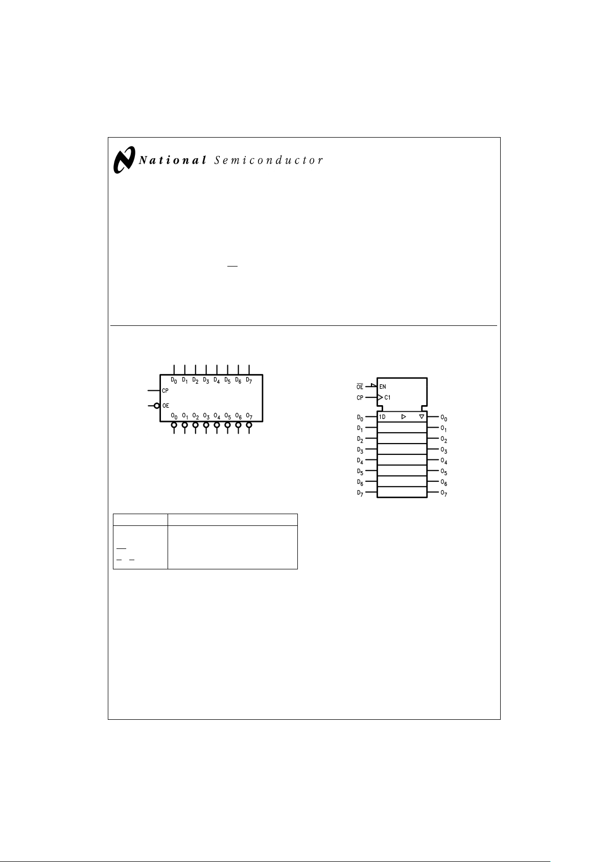
Logic Symbols
Pin Names Description
D
0–D7
Data Inputs
CP Clock Pulse Input
OE
TRI-STATE Output Enable Input
O
0–O7
Complementary TRI-STATE Outputs
TRI-STATE®is a registered trademarkof National Semiconductor Corporation.
FACT
™
is a trademark of Fairchild Semiconductor Corporation.
DS100292-1
IEEE/IEC
DS100292-2
July 1998
54ACT534 Octal D Flip-Flop with TRI-STATE Outputs
© 1998 National Semiconductor Corporation DS100292 www.national.com

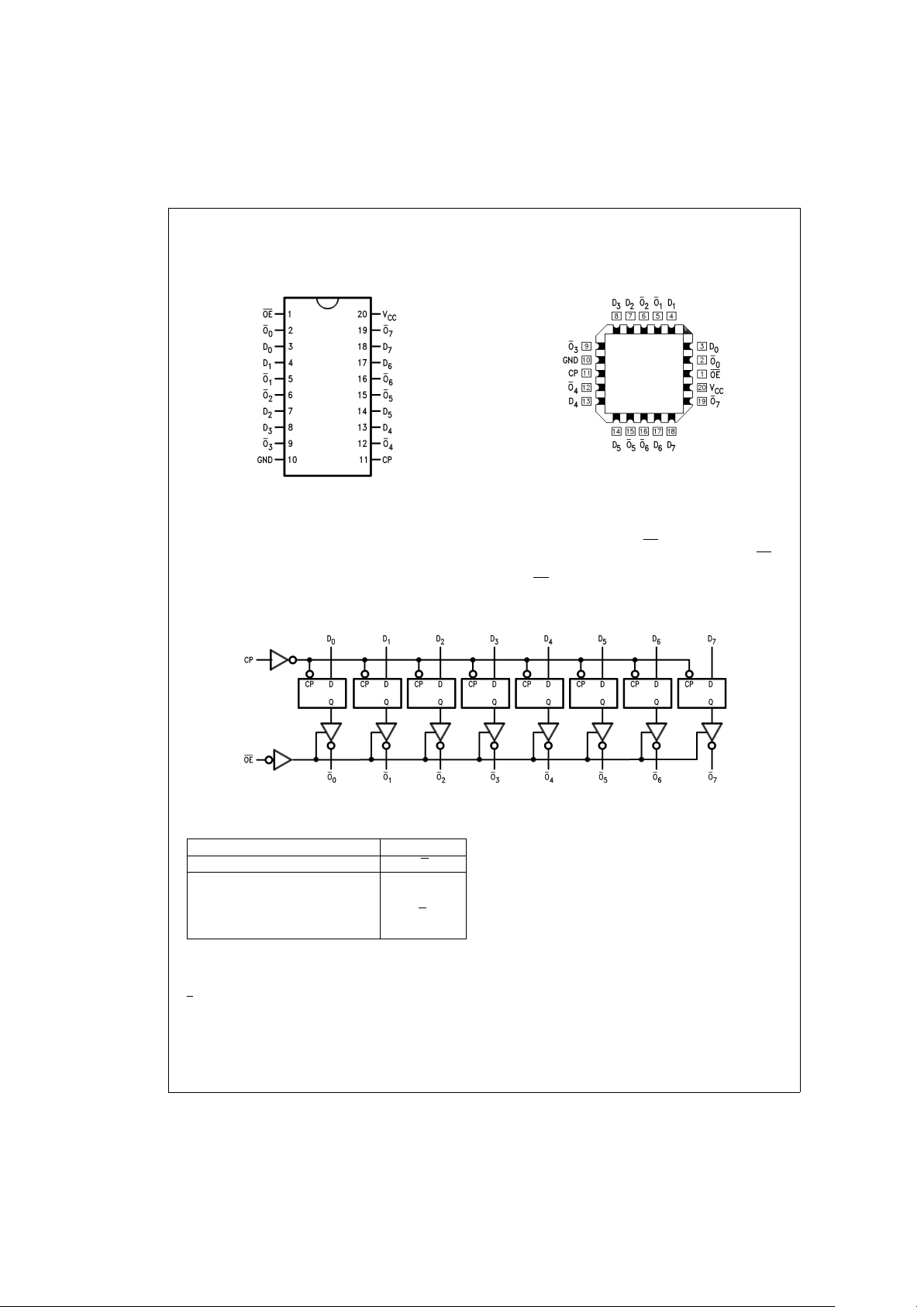
Connection Diagrams
Functional Description
The ’ACT534 consists of eight edge-triggered flip-flops with
individual D-type inputs and TRI-STATEcomplementary outputs. The buffered clock and buffered Output Enable are
common to all flip-flops. The eight flip-flops will store the
state of their individual D inputs that meet thesetup and hold
times requirements on the LOW-to-HIGH Clock (CP) transition. With the Output Enable (OE) LOW, the contents of the
eight flip-flops are available at the outputs. When the OE is
HIGH, the outputs go to the high impedance state. Operation
of the OE input does not affect the state of the flip-flops.
Logic Diagram
Function Table
Inputs Output
CP OE D O
N
LH L
N
LL H
LLX O
0
XHX Z
H
=
HIGH Voltage Level
L=LOW Voltage Level
X=Immaterial
N
=
LOW-to-HIGH Clock Transition
Z=High Impedance
O
0
=
Value stored from previous clock cycle
Pin Assignment
for DIP and Flatpak
DS100292-3
Pin Assignment
for LCC
DS100292-4
DS100292-5
Please note that this diagram is provided only for the understanding of logic operations and should not be used to estimate propagation delays.
www.national.com 2
 Loading...