

NSC 54F574DMQB Datasheet
TL/F/9567
54F/74F574 Octal D-Type Flip-Flop with TRI-STATE Outputs
May 1995
54F/74F574
Octal D-Type Flip-Flop with TRI-STATE
É
Outputs
General Description
The ’F574 is a high-speed, low power octal flip-flop with a
buffered common Clock (CP) and a buffered common Output Enable (OE
). The information presented to the D inputs
is stored in the flip-flops on the LOW-to-HIGH Clock (CP)
transition.
This device is functionally identical to the ’F374 except for
the pinouts.
Features
Y
Inputs and outputs on opposite sides of package
allowing easy interface with microprocessors
Y
Useful as input or output port for microprocessors
Y
Functionally identical to ’F374
Y
TRI-STATE outputs for bus-oriented applications
Commercial Military
Package
Package Description
Number
74F574PC N20A 20-Lead (0.300×Wide) Molded Dual-In-Line
54F574DM (Note 2) J20A 20-Lead Ceramic Dual-In-Line
74F574SC (Note 1) M20B 20-Lead (0.300×Wide) Molded Small Outline, JEDEC
74F574SJ (Note 1) M20D 20-Lead (0.300×Wide) Molded Small Outline, EIAJ
54F574FM (Note 2) W20A 20-Lead Cerpack
54F574LM (Note 2) E20A 20-Lead Ceramic Leadless Chip Carrier, Type C
Note 1: Devices also available in 13×reel. Use suffixeSCX and SJX.
Note 2: Military grade device with environmental and burn-in processing. Use suffix
e
DMQB, FMQB and LMQB.
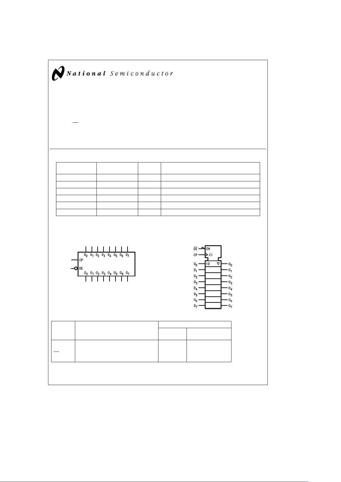
Logic Symbols
TL/F/9567– 1
IEEE/IEC
TL/F/9567– 4
Unit Loading/Fan Out
54F/74F
Pin Names Description
U.L. Input I
IH/IIL
HIGH/LOW Output IOH/I
OL
D0–D
7
Data Inputs 1.0/1.0 20 mA/b0.6 mA
CP Clock Pulse Input (Active LOW) 1.0/1.0 20 mA/
b
0.6 mA
OE
TRI-STATE Output Enable Input (Active LOW) 1.0/1.0 20 mA/b0.6 mA
O
0–O7
TRI-STATE Outputs 150/40 (33.3)b3 mA/24 mA (20 mA)
TRI-STATEÉis a registered trademark of National Semiconductor Corporation.
C
1995 National Semiconductor Corporation RRD-B30M75/Printed in U. S. A.

Connection Diagrams
Pin Assignment
for DIP, SOIC and Flatpak
TL/F/9567– 2
Pin Assignment
for LCC
TL/F/9567– 3
Functional Description
The ’F574 consists of eight edge-triggered flip-flops with individual D-type inputs and TRI-STATE true outputs. The
buffered clock and buffered Output Enable are common to
all flip-flops. The eight flip-flops will store the state of their
individual D inputs that meet the setup and hold times requirements on the LOW-to-HIGH Clock (CP) transition. With
the Output Enable (OE
) LOW, the contents of the eight flip-
flops are available at the outputs. When OE
is HIGH, the
outputs go to the high impedance state. Operation of the
OE
input does not affect the state of the flip-flops.
Function Table
Inputs Internal Outputs
Function
OE CP D Q O
H H L NC Z Hold
H H H NC Z Hold
H L L L Z Load
H L H H Z Load
L L L L L Data Available
L L H H H Data Available
L H L NC NC No Change in Data
L H H NC NC No Change in Data
HeHIGH Voltage Level
L
e
LOW Voltage Level
X
e
Immaterial
Z
e
High Impedance
L
e
LOW-to-HIGH Transition
NC
e
No Change
Logic Diagram
TL/F/9567– 5
Please note that this diagram is provided only for the understanding of logic operations and should not be used to estimate propagation delays.
2

Absolute Maximum Ratings (Note 1)
If Military/Aerospace specified devices are required,
please contact the National Semiconductor Sales
Office/Distributors for availability and specifications.
Storage Temperature
b
65§Ctoa150§C
Ambient Temperature under Bias
b
55§Ctoa125§C
Junction Temperature under Bias
b
55§Ctoa175§C
Plastic
b
55§Ctoa150§C
V
CC
Pin Potential to
Ground Pin
b
0.5V toa7.0V
Input Voltage (Note 2)
b
0.5V toa7.0V
Input Current (Note 2)
b
30 mA toa5.0 mA
Voltage Applied to Output
in HIGH State (with V
CC
e
0V)
Standard Output
b
0.5V to V
CC
TRI-STATE Output
b
0.5V toa5.5V
Current Applied to Output
in LOW State (Max) twice the rated I
OL
(mA)
Note 1: Absolute maximum ratings are values beyond which the device may
be damaged or have its useful life impaired. Functional operation under
these conditions is not implied.
Note 2: Either voltage limit or current limit is sufficient to protect inputs.
Recommended Operating
Conditions
Free Air Ambient Temperature
Military
b
55§Ctoa125§C
Commercial 0
§
Ctoa70§C
Supply Voltage
Military
a
4.5V toa5.5V
Commercial
a
4.5V toa5.5V
DC Electrical Characteristics
Symbol Parameter
54F/74F
Units V
CC
Conditions
Min Typ Max
V
IH
Input HIGH Voltage 2.0 V Recognized as a HIGH Signal
V
IL
Input LOW Voltage 0.8 V Recognized as a LOW Signal
V
CD
Input Clamp Diode Voltage
b
1.2 V Min I
IN
eb
18 mA
V
OH
Output HIGH 54F 10% V
CC
2.5 I
OH
eb
1mA
Voltage 54F 10% V
CC
2.4 I
OH
eb
3mA
74F 10% V
CC
2.5
V Min
I
OH
eb
1mA
74F 10% V
CC
2.4 I
OH
eb
3mA
74F 5% V
CC
2.7 I
OH
eb
1mA
74F 5% V
CC
2.7 I
OH
eb
3mA
V
OL
Output LOW 54F 10% V
CC
0.5
V Min
I
OL
e
20 mA
Voltage 74F 10% V
CC
0.5 I
OL
e
24 mA
I
IH
Input HIGH 54F 20.0
mA Max
V
IN
e
2.7V
Current 74F 5.0
I
BVI
Input HIGH Current 54F 100
mA Max
V
IN
e
7.0V
Breakdown Test 74F 7.0
I
CEX
Output HIGH 54F 250
mA Max
V
OUT
e
V
CC
Leakage Current 74F 50
V
ID
Input Leakage
74F 4.75 V 0.0
I
ID
e
1.9 mA
Test All Other Pins Grounded
I
OD
Output Leakage
74F 3.75 mA 0.0
V
IOD
e
150 mV
Circuit Current All Other Pins Grounded
I
IL
Input LOW Current
b
0.6 mA Max V
IN
e
0.5V
I
OZH
Output Leakage Current 50 mA Max V
OUT
e
2.7V
I
OZL
Output Leakage Current
b
50 mA Max V
OUT
e
0.5V
I
OS
Output Short-Circuit Current
b
60
b
150 mA Max V
OUT
e
0V
I
ZZ
Bus Drainage Test 500 mA 0.0V V
OUT
e
5.25V
I
CCZ
Power Supply Current 55 86 mA Max V
O
e
HIGH Z
3
 Loading...