

NSC 54F38LMQB, 54F38FMQB, 54F38DMQB, 54F38DM, 54F38DC Datasheet

TL/F/9465
54F/74F38 Quad Two-Input NAND Buffer (Open Collector)
December 1994
54F/74F38
Quad Two-Input NAND Buffer
(Open Collector)
General Description
This device contains four independent gates, each of which
performs the logic NAND function. The open-collector outputs require external pull-up resistors for proper logical operation.
Commercial Military
Package
Package Description
Number
74F38PC N14E 14-Lead (0.300×Wide) Molded Dual-In-Line
54F38DM (Note 2) J14A 14-Lead Ceramic Dual-In-Line
74F38SC (Note 1) M14A 14-Lead (0.150×Wide) Molded Small Outline, JEDEC
74F38SJ (Note 1) M14D 14-Lead (0.300×Wide) Molded Small Outline, EIAJ
54F38FM (Note 2) W14B 14-Lead Cerpack
54F38LM (Note 2) E20A 20-Lead Ceramic Leadless Chip Carrier, Type C
Note 1: Devices also available in 13×reel. Use suffixeSCX and SJX.
Note 2: Military grade device with environmental and burn-in processing. Use suffix
e
DMQB, FMQB and LMQB.
Logic Symbol Connection Diagrams
IEEE/IEC
TL/F/9465– 3
Pin Assignment
for DIP, SOIC and Flatpak
TL/F/9465– 1
Pin Assignment
for LCC
TL/F/9465– 2
TRI-STATEÉis a registered trademark of National Semiconductor Corporation.
C
1995 National Semiconductor Corporation RRD-B30M75/Printed in U. S. A.
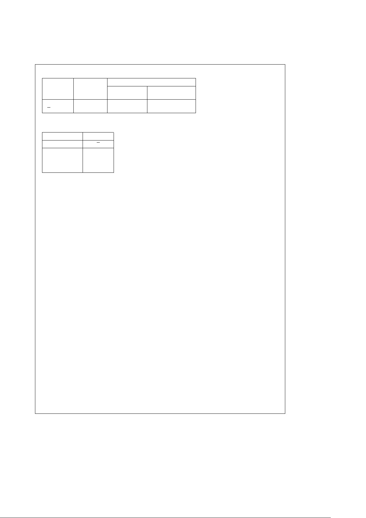
Unit Loading/Fan Out
54F/74F
Pin Names Description
U.L. Input I
IH/IIL
HIGH/LOW Output IOH/I
OL
An,B
n
Inputs 1.0/2.0 20 mA/b1.2 mA
O
n
Outputs OC*/106.6 (80) OC*/64 mA (48 mA)
*OCeOpen Collector
Function Table
Inputs Output
AB O
LL H
LH H
HL H
HH L
H
e
HIGH Voltage Level
L
e
LOW Voltage Level
2

Absolute Maximum Ratings (Note 1)
If Military/Aerospace specified devices are required,
please contact the National Semiconductor Sales
Office/Distributors for availability and specifications.
Storage Temperature
b
65§Ctoa150§C
Ambient Temperature under Bias
b
55§Ctoa125§C
Junction Temperature under Bias
b
55§Ctoa175§C
Plastic
b
55§Ctoa150§C
V
CC
Pin Potential to
Ground Pin
b
0.5V toa7.0V
Input Voltage (Note 2)
b
0.5V toa7.0V
Input Current (Note 2)
b
30 mA toa5.0 mA
Voltage Applied to Output
in HIGH State (with V
CC
e
0V)
Standard Output
b
0.5V to V
CC
TRI-STATEÉOutput
b
0.5V toa5.5V
Current Applied to Output
in LOW State (Max) twice the rated I
OL
(mA)
Note 1: Absolute maximum ratings are values beyond which the device may
be damaged or have its useful life impaired. Functional operation under
these conditions is not implied.
Note 2: Either voltage limit or current limit is sufficient to protect inputs.
Recommended Operating
Conditions
Free Air Ambient Temperature
Military
b
55§Ctoa125§C
Commercial 0
§
Ctoa70§C
Supply Voltage
Military
a
4.5V toa5.5V
Commercial
a
4.5V toa5.5V
DC Electrical Characteristics
Symbol Parameter
54F/74F
Units V
CC
Conditions
Min Typ Max
V
IH
Input HIGH Voltage 2.0 V Recognized as a HIGH Signal
V
IL
Input LOW Voltage 0.8 V Recognized as a LOW Signal
V
CD
Input Clamp Diode Voltage
b
1.2 V Min I
IN
eb
18 mA
V
OL
Output LOW 54F 10% V
CC
0.55
V Min
I
OL
e
48 mA
Voltage 74F 10% V
CC
0.55 I
OL
e
64 mA
I
IH
Input HIGH 54F 20.0
mA Max
V
IN
e
2.7V
Current 74F 5.0
I
BVI
Input HIGH Current 54F 100
mA Max
V
IN
e
7.0V
Breakdown Test 74F 7.0
V
ID
Input Leakage
74F 4.75 V 0.0
I
ID
e
1.9 mA
Test All Other Pins Grounded
I
OD
Output Leakage
74F 3.75 m A 0.0
V
IOD
e
150 mV
Circuit Current All Other Pins Grounded
I
IL
Input LOW Current
b
1.2 mA Max V
IN
e
0.5V
I
OHC
Open Collector, Output
250 mA Min
V
OUT
e
V
CC
OFF Leakage Test
I
CCH
Power Supply Current 2.1 7.0 mA Max V
O
e
HIGH
I
CCL
Power Supply Current 26.0 30.0 mA Max V
O
e
LOW
3
 Loading...