

Page 1

Nokia Customer Care
RH-29 Series Cellular Phones
7 - System Module and User
Interface
Issue 1 05/2004 Copyright © 2004 Nokia Corporation Page 1
Company Confidential
Page 2

RH-29 Company Confidential
7 - System Module Nokia Customer Care
Table of Contents
Page No
1BQ System Module Block Diagram ............................................................................ 6
Baseband Technical Summary....................................................................................... 7
Functional Description................................................................................................... 8
BB description .............................................................................................................8
Memory configuration............................................................................................... 8
Energy management.................................................................................................. 8
Modes of operation ......................................................................................................8
Voltage limits............................................................................................................ 9
Clocking scheme ..........................................................................................................9
UPP_WD2 voltage/clock frequency adjusting........................................................ 10
Power distribution, control and reset .........................................................................10
Power-up sequence (reset mode)............................................................................. 10
Powering off............................................................................................................ 11
Uncontrolled powering off...................................................................................... 11
Watchdogs............................................................................................................... 11
Charging.................................................................................................................. 11
Chargers .................................................................................................................. 12
Battery..................................................................................................................... 12
Back-up battery and real time clock ..........................................................................12
Baseband measurement A/D converter .....................................................................12
ZOCUS ......................................................................................................................12
RH-29 BB Features & HW Interfaces ......................................................................... 14
RH-29 BB user interface ...........................................................................................14
UI module interface................................................................................................. 14
Bluetooth ....................................................................................................................14
SIM interface .............................................................................................................14
MMC interface ...........................................................................................................14
RH-29 audio concept .................................................................................................14
Earpiece................................................................................................................... 15
Microphone ............................................................................................................. 15
Audio amplifier and MALT speaker....................................................................... 16
External audio interface .......................................................................................... 16
Flashing ......................................................................................................................17
Testing interfaces .......................................................................................................17
Extreme voltages ......................................................................................................18
Temperature conditions .............................................................................................18
Humidity and water resistance ...................................................................................18
RF Characteristics of RH-29 ....................................................................................... 19
RF Power Distribution ...............................................................................................20
Channel Numbers and Frequencies ...........................................................................22
Main RF characteristics .............................................................................................22
Transmitter Characteristics ........................................................................................22
Receiver Characteristics ............................................................................................22
RF block diagram ......................................................................................................23
Receiver .....................................................................................................................24
Rx Signal paths........................................................................................................ 24
Antenna switch........................................................................................................ 24
Page 2 Copyright © 2004 Nokia Corporation Issue 1 05/2004
Company Confidential
Page 3

Company Confidential RH-29
Nokia Customer Care 7 - System Module
Receiver................................................................................................................... 25
GSM900 Transmitter .................................................................................................26
TX Path of the transmitted GSM900 signal............................................................ 26
GSM900 TX path of Mjoelner RF ASIC................................................................ 26
GSM900 TX path of the Power Amplifier (PA)..................................................... 27
Antenna Switch (TX/RX switch)............................................................................ 27
GSM1800 Transmitter ...............................................................................................29
Path of the transmitted 1800 signal......................................................................... 29
The path of Mjoelner RF ASIC............................................................................... 29
The path of the PA .................................................................................................. 29
Antenna Switch....................................................................................................... 30
Synthesizer................................................................................................................... 31
26 MHz reference oscillator (VCXO) .......................................................................31
VCO ...........................................................................................................................31
PLL Block diagram ....................................................................................................32
Frequency synthesizers ..............................................................................................33
Receiver .....................................................................................................................33
Transmitter .................................................................................................................33
Front End................................................................................................................. 33
Power amplifier....................................................................................................... 34
RF ASIC Helgo ..........................................................................................................34
AFC function .............................................................................................................35
Antenna ......................................................................................................................35
User Interface............................................................................................................... 36
Issue 1 05/2004 Copyright © 2004 Nokia Corporation Page 3
Company Confidential
Page 4

RH-29 Company Confidential
7 - System Module Nokia Customer Care
List of abbreviations
ASIC Application Specific Integrated Circuit
BB Baseband
BLUETOOTH, BT Bluetooth
BSI Battery Size Indicator
CBus Control Bus connecting UPP_WD2 with UEM
CCP Compact Camera Port
CPU Central Processing Unit
DBUS Data Bus
DSP Digital Signal Processor
EGSM Extended – GSM
ESD Electro Static Discharge
GPRS General Packet Radio Service
GSM Group Special Mobile/Global system mobile
HF Hands free
HFCM Handsfree Common
HS Handset
I/O Input/Output
IHF Integrated hands free
IR Infra red
IrDA Infrared Association
LCD Liquid Crystal Display
LO Local Oscillator
MCU Micro Controller Unit
Page 4 Copyright © 2004 Nokia Corporation Issue 1 05/2004
Company Confidential
Page 5

Company Confidential RH-29
Nokia Customer Care 7 - System Module
MIC, mic Microphone
PA Power Amplifier
DCS GSM1800
PDA Pocket Data Application
PWB Printed Wiring Board
PLL Phase Locked Loop
PWB Printed Wired Board
RFBUS Control Bus For RF RXReceiver
SDRAM Synchronous Dynamic Random Access Memory
SIM Subscriber Identity Module
TX Transmitter
UEM Universal Energy Management
UHF Ultra High Frequency
UI User Interface
VCO Voltage controlled oscillator
VHF Very High Frequency
VCXO Voltage Controlled Crystal Oscillator
VGA Video Graphics Array
Issue 1 05/2004 Copyright © 2004 Nokia Corporation Page 5
Company Confidential
Page 6
RH-29 Company Confidential
7 - System Module Nokia Customer Care
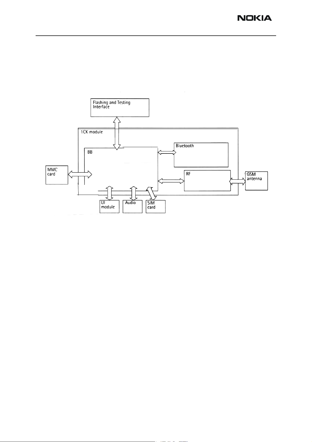
1BQ System Module Block Diagram
The 1BQ System module is the engine board of the RH-29 phone. It includes the baseband and RF functions of the phone and the Bluetooth module, fig. 1 below. External
interfaces are drawn as arrows crossing 1BQ border.
Figure 1: 1BQ module block diagram
The Accessory interface is provided by Bluetooth. Only the Headset & Charger are galvanic interfaces.
Page 6 Copyright © 2004 Nokia Corporation Issue 1 05/2004
Company Confidential
Page 7

Company Confidential RH-29
Nokia Customer Care 7 - System Module
Baseband Technical Summary
The heart of the BB is UPP_WD2, which includes the MCU, DSP and Digital Control Logic.
Power is supplied by the UEMK ASIC and a number of discrete regulators. Memory comprises of 2x 64Mbit (16Mbytes) Flash Memory Devices and 128 Mbit (16 Mbytes)
SDRAM.
There are two audio transducers (Earpiece 8 mm and a MALT Speaker 16 mm) and External Galvanic Headset (DCT4) interface. MALT Speaker is also used to handle the ring tone.
The MALT Speaker is driven by a discrete audio amplifier. In RH-29 there is only one
microphone for both HS and IHF modes.
For Data connectivity there is the Bluetooth and an MMC card.
The Display is a GD82 type Colour Display with 66000 Colours and 176x208 pixels with
backlighting.
Issue 1 05/2004 Copyright © 2004 Nokia Corporation Page 7
Company Confidential
Page 8

RH-29 Company Confidential
7 - System Module Nokia Customer Care
Functional Description
BB description
The BB Core is based on UPP_WD2 CPU, which is a PDA version of the DCT4 UPP ASIC.
UPP_WD2 takes care of all the signal processing and operation controlling tasks of the
phone as well as all PDA tasks.
For power management there is one main ASIC for controlling charging and supplying
power UEM plus some discrete power supplies. The main reset for the system is generated by the UEM.
The interface to the RF and audio sections is also handled by the UEM. This ASIC provides
A/D and D/A conversion of the in-phase and quadrature receive and transmit signal
paths and also A/D and D/A conversions of received and transmitted audio signals. Data
transmission between UEM and RF and the UPP_WD2 is implemented using different
serial connections (CBUS, DBUS and RFBUS). Digital speech processing is handled by
UPP_WD2 ASIC.
A real time clock function is integrated into UEM, which utilizes the same 32kHz-clock
source as the sleep clock. A rechargeable battery provides backup power to run the RTC
when the main battery is removed. Backup time is about 3 hours.
Memory configuration
RH-29 uses two kinds of memories, Flash and SDRAM. These Memories have their own
dedicated bus interfaces to UPP_WD2.
Synchronous DRAM is used as working memory. Interface is 16 bit wide data and 14 bit
Address. Memory clocking speed is 104 MHz. The SDRAM size 128Mbits (8Mx16).
SDRAM I/O is 1.8 V and core 2.78 V supplied by UEM regulator VIO. All memory contents
are lost if the supply voltage is switched off.
Multiplexed Flash Memory Interface is used to store the MCU program code and User
Data. The memory interface is a burst type FLASH with multiplexed address/data bus,
running at 104/3MHz.
Both Flash I/O and core voltage are 1.8 V supplied by UEM’s VIO.
Energy management
The master of EM control is UEM and with SW this has the main control of the system
voltages and operating modes.
Modes of operation
RH-29 employs several hardware & SW controlled operation modes. Main Modes are
described below.
• NO_SUPPLY mode means that the main battery is not present or its
Page 8 Copyright © 2004 Nokia Corporation Issue 1 05/2004
Company Confidential
Page 9
Company Confidential RH-29
Nokia Customer Care 7 - System Module
voltage is too low (below UEM master reset threshold) and back-up battery voltage is too low.
• In BACK_UP mode the main battery is not present or its voltage is too
low but back-up battery has sufficient charge in it.
• In PWR_OFF mode the main battery is present and its voltage is over
UEM master reset threshold. All regulators are disabled.
• RESET mode is a synonym for start-up sequence and contains in fact
several modes. In this mode regulators and oscillators are enabled and
after they have stabilized system reset is released and PWR_ON mode
entered.
• In PWR_ON mode SW is running and controlling the system.
• SLEEP mode is entered from PWR_ON mode when the system’s activity is low (SLEEPX controlled by SW).
• FLASHING mode is for production SW download.
Voltage limits
In the following the voltage limits of the system are listed. These are also controlling system states.:
Parameter Description Value
V
MSTR+
V
MSTR-
V
COFF+
V
COFF-
V_BU
V_BU
SW
COFF
COFF+
COFF-
Master reset threshold (rising) 2.1 V (typ.)
Master reset threshold (falling) 1.9 V (typ.)
Hardware cutoff (rising) 3.1 V (typ.)
Hardware cutoff (falling) 2.8 V (typ.)
Back-up battery cutoff (rising) 2.1 V (typ.)
Back-up battery cutoff (falling) 2.0 V (typ.)
SW cutoff limit (> regulator drop-out limit) MIN! 3.4 V SW changeable
The master reset threshold controls the internal reset of UEM. If battery voltage is above
V
, UEM’s charging control logic is alive. Also, RTC is active and supplied from the
MSTR
main battery. Above V
UEM allows the system to be powered on although this may
MSTR
not succeed due to voltage drops during start-up. SW can also consider battery voltage
too low for operation and power down the system.
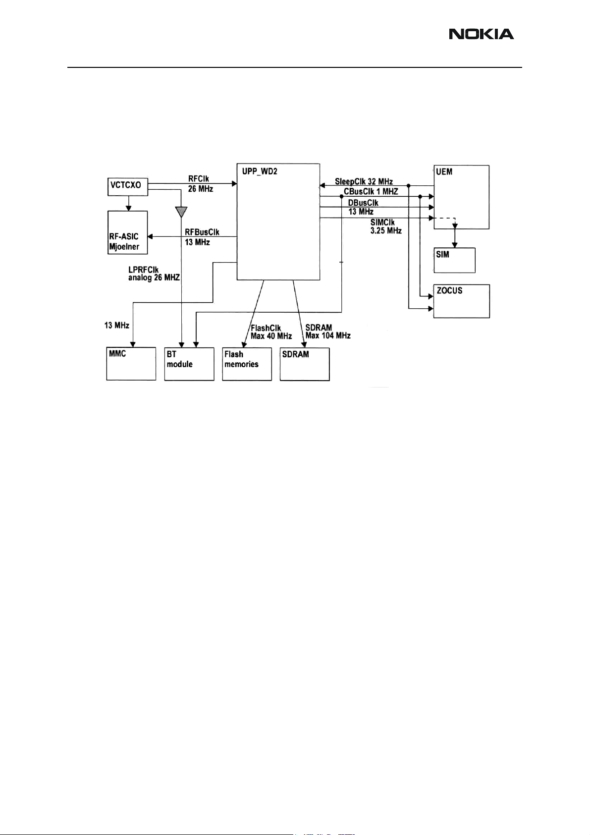
Clocking scheme
A 26 MHz VCXO is used as system clock generator in GSM. During the system start-up,
UEM RC-oscillators generate timing for state machines. All clock signals of the engine
Issue 1 05/2004 Copyright © 2004 Nokia Corporation Page 9
Company Confidential
Page 10
RH-29 Company Confidential
7 - System Module Nokia Customer Care
are illustrated in following figure.
Bluetooth uses 26 MHz clock.
Figure 2: RH-29 Clocking.
In SLEEP mode the VCXO is off. UEM generates low frequency clock signal (32.768 kHz)
that is fed to UPP_WD2, Bluetooth and ZOCUS.
UPP_WD2 voltage/clock frequency adjusting
No external clock is available for UPP_WD2 before VCXO starts. As reset is released, the
VCXO is running and MCU uses the 26 MHz clock while DSP is in reset. There are three
identical DPLL's, for MCU, for DSP and for accessory interfaces, which can be controlled
independently. The clock for MCU can be up to 104 MHz and 117 MHz is maximum clock
Frequency for the DSP. These clock signals are used either directly (SDRAM IF) or divided
down for the interfaces (e.g. flash IF).
Power distribution, control and reset
All power (except backup battery power) is drawn from the BL6-C Li-Ion battery located
in the B cover. Current flows through ZOCUS current sense resister which is used for current measurement by ZOCUS and thus for remaining operating time estimation.
1BQ board contains one power ASIC, UEM and discrete regulators needed for generating
the different operating voltages. The discrete regulators consist of an step-down DC-DC
converter to power UPPWD2 voltage core and a step-up DC-DC converter for display
module backlighting. The keyboard backlighting is powered with a discrete driver.
Power-up sequence (reset mode)
RESET mode can be entered in four ways: by inserting the battery or charger, by RTC
alarm or by pressing the power key. The VCXO is Powered by UEM. After a 220 ms delay
regulators are configured and UEM enters PWR_ON mode and system reset PURX is
Page 10 Copyright © 2004 Nokia Corporation Issue 1 05/2004
Company Confidential
Page 11

Company Confidential RH-29
Nokia Customer Care 7 - System Module
released.
During system start-up, in RESET state, the regulators are enabled, and each regulator
charges the capacitor(s) at the output with the maximum current (short circuit current)
it can deliver. This results in battery voltage dropping during start-up. When a battery
with voltage level just above the hardware cutoff limit is inserted, the system may not
start due to excessive voltage dipping. Dropping below 2.8 V for longer than 5 us forces
the system to PWR_OFF state.
Powering off
Controlled powering off is done when the user requests it by pressing the power-key or
when the battery voltage falls too low. Uncontrolled powering off happens when the
battery is suddenly removed or if over-temperature condition is detected in regulator
block while in RESET mode. Then all UEM’s regulators are disabled immediately and discrete regulators are disabled as Vbat supply disappears.
Controlled powering off
For RH-29 powering off is initiated by pressing the power key and Power off sequence is
activated in UEM and SW. Basically Power key cause UEM Interrupt to UPP_WD2 and SW
sets Watchdog time value to zero and as this happens, PURX is forced low and all regulators are disabled.
If the battery voltage falls below the very last SW-cutoff level, SW will power off the
system by letting the UEM’s watchdog elapse.
If thermal shutdown limit in UEM regulator block is exceeded, the system is powered off.
System reset PURX is forced low.
Uncontrolled powering off
This happens when the battery is suddenly removed. UEM’s state machine notices battery
removal after battery voltage has been below V
PURX is set low and all UEM’s regulators are disabled.
Watchdogs
There are three watchdogs in UEM. The first one is for controlling system power-on and
power-down sequences. The initial time for this watchdog after reset is 32 s and the
watchdog can not be disabled. The time can be set using a register. This watchdog is used
for powering the system off in a controlled manner. The other one is for security block
and is used during IMEI code setting. The third one is a power key watchdog. It is used to
power off the system in case SW is stuck and the user presses the power key. This WD is
SW configurable.
for 5 us and enters PWR_OFF mode.
COFF-
There is also a”soft watchdog” in UPP_WD2. It is used to reset the chip in case software
gets stuck for any reason. The Bluetooth module also contains a watchdog.
Charging
Charging control and charge switch is in UEM. There are two different charging modes;
Issue 1 05/2004 Copyright © 2004 Nokia Corporation Page 11
Company Confidential
Page 12

RH-29 Company Confidential
7 - System Module Nokia Customer Care
charging empty battery (start-up charge mode), and SW controlled charging.
UEM digital part takes care of charger detection (generates interrupt to UPP_WD2),
pulse width modulated charging control (for internal charge switch) and over voltage
and current detection. SW using registers controls all these.
Chargers
RH-29 BB supports a standard charger (two wires), Chargers ACP-8 and ACP-12, Cigarette Charger LCH-8 and LCH-12 are supported.
Battery
RH-29 Battery is a detachable, semi-fixed Lithium-Ion BL6-C battery. Nominal voltage is
thus 3.7 V (max charging voltage 4.2 V).
The interface consists of three pins: VBAT, GND and BSI. Pull-down resistor inside of the
batteries (BSI signal) recognizes the battery types. Voltage level at BSI line is measured
using UEM's AD-converter.
Back-up battery and real time clock
Real time clock (RTC), crystal oscillator and back-up battery circuitry reside in UEM. A
register in UEM controls back-up battery charging and charging is possible only in
POWER_ON State.
Baseband measurement A/D converter
UEM contains 11 channels A/D converter, which is used for different Baseband measurement purposes. The resolution of A/D converter is 10 bits. Converter uses the CBUS interface clock signal for the conversion. An interrupt will be given to the MCU at the end of
the measurements. The Converter is used for following purposes.
• Battery Voltage Measurement A/D Channel (Internal)
• Charger Voltage Measurement A/D Channel (Internal)
• Charger Current Measurement A/D Channel (Internal)
• Battery Temperature Measurement A/D Channel (External)
• Battery Size Measurement A/D Channel (External)
• LED Temperature measurement A/D Channel (External)
There is also auxiliary AD converter in UEM, which is used to monitor RF functions.
ZOCUS
The ZOCUS device is a current sensor used for the battery bar display and for determining
whether the phone is in a high current consuming mode. The ZOCUS device measures the
voltage drop across a sense resistor in the battery voltage line. This sense resistor is
Page 12 Copyright © 2004 Nokia Corporation Issue 1 05/2004
Company Confidential
Page 13

Company Confidential RH-29
Nokia Customer Care 7 - System Module
formed from a PWB track and is on an internal layer of the PWB. The sense resistor must
be located close to the battery terminals so that all of the phones current flow through
it. The nominal value of the sense resistor is 3.3 mohm. ZOCUS reports the current measurement to UPP_WD2 via the Cbus interface.
Issue 1 05/2004 Copyright © 2004 Nokia Corporation Page 13
Company Confidential
Page 14

RH-29 Company Confidential
7 - System Module Nokia Customer Care
RH-29 BB Features & HW Interfaces
RH-29 BB user interface
UI module interface
The UI-Module consists of the LCD and keymat. The Colour Display resolution is 176 x
208 and backlighting is via 4 white LED’s with lightguide. The display is connected to the
1BQ module via an 18 pin plug and socket. The keymat is connected to 1BQ by 20-pin
Board-to-Board connector. Interface also includes power rails for keypad backlight. The
keymat interface uses GPIO pins of UPP_WD2.
Bluetooth
Bluetooth provides a fully digital link for communication between a master unit and one
or more slave units. The system provides a radio link that offers a high degree of flexibility to support various applications and product scenarios. Data and control interface for
a low power RF module is provided. Data rate is regulated between the master and the
slave.
SIM interface
The SIM interface is located in two chips (UPP_WD2 and UEM). In UEM there is only support for one SIM card. The interfaces support both 1.8 V and 3 V SIM cards. Adjustable
SIM regulator (1.8V/3.0V) is located in UEM and can be controlled by SW.
The data communication between the card and the phone is asynchronous half duplex.
The clock supplied to the card is 3.25 MHz. The data baud rate is SIM card clock frequency divided by 372 (by default), 64, 32 or 16.
MMC interface
The MMC interface consists of a block in UPP_WD2 plus a level shifting device known as
“Lester” and an EMC protection ASIP. The MMC interface comprises 3 lines -clock, data
and command and runs at 8.66 MHz. The Lester device also incorporates a 2.85V regulator to power the MMC card.
Use only Multimedia cards (MMC) with this device. Other memory cards, such as Secure
Digital (SD) cards, do not fit in the MMC card slot and are not compatible with this
device.
Using an incompatible memory card may damage the memory card as well as device, and
data stored on the incompatible card may be corrupted.
RH-29 audio concept
RH-29 Audio includes earpiece, microphone, and headset connector and MALT speaker.
Audio is based on ASIC's UPP_WD2, UEM and a discrete amplifier for the handsfree
speaker known as “boomer”.
Page 14 Copyright © 2004 Nokia Corporation Issue 1 05/2004
Company Confidential
Page 15

Company Confidential RH-29
Nokia Customer Care 7 - System Module
Figure 3: RH-29 Audio Blocks
Between UPP_WD2 and UEM the audio signals are transferred in digital format using
signals MICDATA and EARDATA. The headset output of UEM is also fed to boomer i.e. the
MALT speaker and the headset share the same output lines from UEM. Ringing tones and
warning/info tones are produced with the MALT speaker also.
Earpiece
The earpiece to be used in RH-29 is an 8-mm Pico earpiece produced by Philips Speaker
Systems. It has 32Ω continuous impedance and continuous power 8 mWatt. It's driven
by differential signals from UEM (EARP & EARN). It makes contact with the PWB via
spring contacts.
Microphone
The microphone capsule for RH-29 a BEETLE EMC microphone. It has sensitivity of -42db
Nominal. Contacts are done by springs.
Two inputs are used from UEM, one for normal internal microphone and a second for
headset. The third microphone input is not used, so it is connected to ground via capacitors. Microphone bias block in UEM generates bias voltages for handportable and handsFree/headset microphones. For both microphone bias outputs (MICB1 & MICB2) the
minimum output voltage is 2.0 Volts and maximum output current is 600 µA. Microphone bias block also includes a low pass filter for the reference voltage used as an input
for the MICB1&2 amplifiers.
Issue 1 05/2004 Copyright © 2004 Nokia Corporation Page 15
Company Confidential
Page 16

RH-29 Company Confidential
7 - System Module Nokia Customer Care
Audio amplifier and MALT speaker
The speaker to be used in RH-29 is a 16mm 8Ω speaker. It can handle 0.2 Watts nominal
Power and Peak power 0.3 Watts. The component is housed in the B cover and connects
to the PWB via spring contacts.
HF and HFCM lines of UEM are use to drive the amplifier.
Power amplifier is a differential opamp. The differential output drives the MALT speaker.
The amplifier load impedance is 8 ohm.
The outputs go into a high impedance state when powered down. The amplifier can be
enabled and shut down using a GENIO line from UPP_WD2.
SW controls IHF and earpiece volume via UEM. Gain setting can be done in 2 dB steps,
from –40 to +6 dB. Output sound pressure level of the MALT speaker is controlled by SW
(CBus is used for controlling).
The schematic around the amplifier is presented in RH-29 schematics. The schematic
shows all the filtering needed and also protection components against ESD and
EMC.EMC and ESD Filtering component must be as near as possible to earphone pads of
the phone.
The supply voltage for the amplifier is taken directly from the battery voltage.
External audio interface
In RH-29 there is Headset Connector which is fully differential 4–wire connection.
2. XEARN
4. XEARP
5. HE A D IN T
3. XM IC P
1. XM IC N
The Handsfree (HF) driver in UEM is meant for headset. In RH-29 case the output is
driven in fully differential mode. In the fully differential mode HF pin is the negative output and HFCM pin is the positive output. The gain of the Handsfree driver in the differential mode is 6 dB. The earpiece (EARP, EARN) and headset (HF, HFCM) signals are
multiplexed so that the outputs can not be used simultaneously. The HF and HFCM
amplifiers include a transient suppression circuitry, which prevents unwanted spikes in
HF and HFCM outputs when switching on and off the amplifiers.
Figure 4: External Audio Connector
The plug will open a mechanical switch inside the connector between HF and HeadInt
lines. The HeadInt line will be pulled up to 2.7V by internal resistor when the switch is
open. When not having the plug inserted the voltage in the HeadInt line will be <0.8 V
caused by internal pull down resistor in the HF line.
Page 16 Copyright © 2004 Nokia Corporation Issue 1 05/2004
Company Confidential
Page 17

Company Confidential RH-29
Nokia Customer Care 7 - System Module
Flashing
SW download in service is implemented by custom tools and SW, kindly refer to Service
Software Instructions and Service Tool section of the manual.
Testing interfaces
Testing interface Electrical Specifications
Pin Name Dir Parameter Min Typ Max Unit Notes
1 MBUS <->Vol 0 0.2 0.3*VFlash1 V
Vil (From Prommer) 0 0.2 0.3*VFlash1 V
Voh 0.7*VFlash1 2.7 0.7*VFlash1 V
Vih(From Prommer) 0.7*VFlash1 2.7 VFlash1 V
2 FBusTx-> Vol 0 2.7 0.3*VFlash1 V
Voh 0.7*VFlash1 2.7 VFlash1 V
3 FBusRx<- Vil (From Prommer) 0 2.7 0.3*VFlash1 V
Vih(FromPrommer) 1.89 2.7 VFlash1 V
Abs. Max. Voltage
to Test Pad Referenced to GND
4 VPP To Phone 0 / 2.8 / 12 +/-3%V Prommer
4 VPP To Phone 0 / 2.8 / 12 +/-3%V Prommer
5 GND 0 V VBAT
-0.3V 3.0 V Absolute Max
Voltage limits
to MBUS/
FBUS
4 VPP
Select
4 VPP
Select
GROUND
Note1: VFlash1 is 2.78 +/- 3%
Electrical Specifications for Power Supply Interface in Prod Testing
Pin Name Min Typ Max Unit Notes
1 VBAT 0 3.6 5.1 V
2 BSI 0 2.78 VFlash1 V Internal pullup
3 GND 0 V
Note 1: VAna & VFlash1 = 2.78 +/-3%
Issue 1 05/2004 Copyright © 2004 Nokia Corporation Page 17
Company Confidential
Page 18

RH-29 Company Confidential
7 - System Module Nokia Customer Care
Extreme voltages
Lithium-Ion battery BL6-C (1 cell):
Nominal voltage is 3.7V
Lower extreme voltage is 2.8V (cut off voltage)
Higher extreme voltage is 4.2V (charging high limit voltage)
Temperature conditions
Specifications are met within range of –10C to +55C ambient temperature. Reduced
operation between [-30] and [+60]. Storage temperature range is of –40C to +85C.
Humidity and water resistance
Relative humidity range is 5 … 95%. Condensed or dripping water may cause intermittent malfunctions. Protection against dripping water have to be implemented in (enclosure) mechanics. Continuous dampness will cause permanent damage to the module.
Page 18 Copyright © 2004 Nokia Corporation Issue 1 05/2004
Company Confidential
Page 19

Company Confidential RH-29
Nokia Customer Care 7 - System Module
RF Characteristics of RH-29
The RF part comprise a multi-band direct conversion transceiver, however, only two
bands are used. Using direct conversion no intermediate frequencies are used for up- or
down- conversion.
The VCO is set to either twice or four times (depending on the band used) the wanted RX
or TX frequency. The VCO frequency is divided by either 2 or 4 and fed to the mixers
(down-conversion) or modulators (up-conversion). Up- and down- conversion is done in
one step, directly between RF frequency and DC. All up and down-conversion takes place
in the RF ASIC named Mjoelner (N601).
Mjoelner RF ASIC also contains PLL and LNAs for all used bands. A DC control section is
included to power and/or to control TX buffers, detector and antenna switch. The Mjoelner RF ASIC is controlled via a serial bus.
Mjoelner RF ASIC contains an integrated VCXO which uses an external 26 MHz Xtal. No
analogue AFC signal is needed. AFC is done via the serial interface of Mjoelner.
The interface between Mjoelner RF ASIC, UPP and Bluetooth uses a 26 MHz reference
clock. An external 26 MHz reference clock buffer is used to drive Bluetooth module.
The RF supports GPRS (General Packed Radio Service), meaning multi-slot operation, this
will not require special equipment or procedures in repair situations.
Issue 1 05/2004 Copyright © 2004 Nokia Corporation Page 19
Company Confidential
Page 20

RH-29 Company Confidential
X
7 - System Module Nokia Customer Care
Figure 5: RF frequency plan
Mjoelner
EGSM: 925-960 MHz
DCS: 1805 - 18 80 MHz
I-signal
Q-signal
RX
DCS: 1710 - 17 85 MHz
EGSM: 880-915 MHz
RF Power Distribution
All power supplies for the RF Unit are generated in the UEM IC (D190). All RF supplies
can be checked either in Mjoelner can or in BB can.
f/4
f/4
f
f
f/2
f/2
f
34203980
MHz
f
PLL
26 MHz
XTal
LPRFCLK
1/1
1/2
RFCLK
I-signal
Q-signal
T
The power supply configuration used is shown in the block diagram below. Values of
voltages are given as nominal outputs of UEM. Currents are typical values
Page 20 Copyright © 2004 Nokia Corporation Issue 1 05/2004
Company Confidential
Page 21

Company Confidential RH-29
(
Nokia Customer Care 7 - System Module
Figure 6: RF Power distribution diagram.
UEM
VR1A
4.7V)
VR2
VR3
VR4
VR5
VR7
VIO
(1.8V)
VBAT
(2.78V)
(2.78V)
(2.78V)
(2.78V)
(2.78V)
VREF01
(1.35V)
Charge Pump Supply : Vddcp(0.5mA)
TX Modulators(85mA), Bias :
Mjolner registers: Vdddig(10uA)
VCXO Supply : Vddxo(2.7mA)
Vddrxf(7mA), Vddrxbb(30mA)
PLL Supplies : Vddpll(0.5mA), Vddlo
External VCO supply (13mA)
26MHz Buffer, logic : Vddbbb(0.7mA),
Bias Reference : VBEXT(-10uA)
Vddtx(8mA)
BT Buffer (1mA)
RX LNA, RX Mjoner BB :
+ Vddpre(36mA)
Vddl(1uA)
PA, Bluetooth
Issue 1 05/2004 Copyright © 2004 Nokia Corporation Page 21
Company Confidential
Page 22

RH-29 Company Confidential
7 - System Module Nokia Customer Care
Channel Numbers and Frequencies
Table 1: GSM900
Freque ncy list NPL - 1 EGSM900
CH TX RX VCO T X VCO RX CH TX RX VCO TX VCO RX CH TX RX VCO TX VCO RX
975 8 80.2 925.2 3520.8 3700.8 1 890.2 935.2 3560.8 3740.8 63 902.6 947.6 3610.4 3790.4
976 8 80.4 925.4 3521.6 3701.6 2 890.4 935.4 3561.6 3741.6 64 902.8 947.8 3611.2 3791.2
977 8 80.6 925.6 3522.4 3702.4 3 890.6 935.6 3562.4 3742.4 65 903.0 948.0 3612.0 3792.0
978 8 80.8 925.8 3523.2 3703.2 4 890.8 935.8 3563.2 3743.2 66 903.2 948.2 3612.8 3792.8
979 8 81.0 926.0 3524.0 3704.0 5 891.0 936.0 3564.0 3744.0 67 903.4 948.4 3613.6 3793.6
980 8 81.2 926.2 3524.8 3704.8 6 891.2 936.2 3564.8 3744.8 68 903.6 948.6 3614.4 3794.4
981 8 81.4 926.4 3525.6 3705.6 7 891.4 936.4 3565.6 3745.6 69 903.8 948.8 3615.2 3795.2
982 8 81.6 926.6 3526.4 3706.4 8 891.6 936.6 3566.4 3746.4 70 904.0 949.0 3616.0 3796.0
983 8 81.8 926.8 3527.2 3707.2 9 891.8 936.8 3567.2 3747.2 71 904.2 949.2 3616.8 3796.8
984 8 82.0 927.0 3528.0 3708.0 10 892.0 937.0 3568.0 3748.0 72 904.4 949.4 3617.6 3797.6
985 8 82.2 927.2 3528.8 3708.8 11 892.2 937.2 3568.8 3748.8 73 904.6 949.6 3618.4 3798.4
986 8 82.4 927.4 3529.6 3709.6 12 892.4 937.4 3569.6 3749.6 74 904.8 949.8 3619.2 3799.2
987 8 82.6 927.6 3530.4 3710.4 13 892.6 937.6 3570.4 3750.4 75 905.0 950.0 3620.0 3800.0
988 8 82.8 927.8 3531.2 3711.2 14 892.8 937.8 3571.2 3751.2 76 905.2 950.2 3620.8 3800.8
989 8 83.0 928.0 3532.0 3712.0 15 893.0 938.0 3572.0 3752.0 77 905.4 950.4 3621.6 3801.6
990 8 83.2 928.2 3532.8 3712.8 16 893.2 938.2 3572.8 3752.8 78 905.6 950.6 3622.4 3802.4
991 8 83.4 928.4 3533.6 3713.6 17 893.4 938.4 3573.6 3753.6 79 905.8 950.8 3623.2 3803.2
992 8 83.6 928.6 3534.4 3714.4 18 893.6 938.6 3574.4 3754.4 80 906.0 951.0 3624.0 3804.0
993 8 83.8 928.8 3535.2 3715.2 19 893.8 938.8 3575.2 3755.2 81 906.2 951.2 3624.8 3804.8
994 8 84.0 929.0 3536.0 3716.0 20 894.0 939.0 3576.0 3756.0 82 906.4 951.4 3625.6 3805.6
995 8 84.2 929.2 3536.8 3716.8 21 894.2 939.2 3576.8 3756.8 83 906.6 951.6 3626.4 3806.4
996 8 84.4 929.4 3537.6 3717.6 22 894.4 939.4 3577.6 3757.6 84 906.8 951.8 3627.2 3807.2
997 8 84.6 929.6 3538.4 3718.4 23 894.6 939.6 3578.4 3758.4 85 907.0 952.0 3628.0 3808.0
998 8 84.8 929.8 3539.2 3719.2 24 894.8 939.8 3579.2 3759.2 86 907.2 952.2 3628.8 3808.8
999 8 85.0 930.0 3540.0 3720.0 25 895.0 940.0 3580.0 3760.0 87 907.4 952.4 3629.6 3809.6
1000 8 85.2 930.2 3540.8 3720.8 26 895.2 940.2 35 80.8 3760.8 88 907.6 952.6 3630.4 3810.4
1001 8 85.4 930.4 3541.6 3721.6 27 895.4 940.4 35 81.6 3761.6 89 907.8 952.8 3631.2 3811.2
1002 8 85.6 930.6 3542.4 3722.4 28 895.6 940.6 35 82.4 3762.4 90 908.0 953.0 3632.0 3812.0
1003 8 85.8 930.8 3543.2 3723.2 29 895.8 940.8 35 83.2 3763.2 91 908.2 953.2 3632.8 3812.8
1004 8 86.0 931.0 3544.0 3724.0 30 896.0 941.0 35 84.0 3764.0 92 908.4 953.4 3633.6 3813.6
1005 8 86.2 931.2 3544.8 3724.8 31 896.2 941.2 35 84.8 3764.8 93 908.6 953.6 3634.4 3814.4
1006 8 86.4 931.4 3545.6 3725.6 32 896.4 941.4 35 85.6 3765.6 94 908.8 953.8 3635.2 3815.2
1007 8 86.6 931.6 3546.4 3726.4 33 896.6 941.6 35 86.4 3766.4 95 909.0 954.0 3636.0 3816.0
1008 8 86.8 931.8 3547.2 3727.2 34 896.8 941.8 35 87.2 3767.2 96 909.2 954.2 3636.8 3816.8
1009 8 87.0 932.0 3548.0 3728.0 35 897.0 942.0 35 88.0 3768.0 97 909.4 954.4 3637.6 3817.6
1010 8 87.2 932.2 3548.8 3728.8 36 897.2 942.2 35 88.8 3768.8 98 909.6 954.6 3638.4 3818.4
1011 8 87.4 932.4 3549.6 3729.6 37 897.4 942.4 35 89.6 3769.6 99 909.8 954.8 3639.2 3819.2
1012 8 87.6 932.6 3550.4 3730.4 38 897.6 942.6 35 90.4 3770.4 100 910.0 955.0 3640.0 3820.0
1013 8 87.8 932.8 3551.2 3731.2 39 897.8 942.8 35 91.2 3771.2 101 910.2 955.2 3640.8 3820.8
1014 8 88.0 933.0 3552.0 3732.0 40 898.0 943.0 35 92.0 3772.0 102 910.4 955.4 3641.6 3821.6
1015 8 88.2 933.2 3552.8 3732.8 41 898.2 943.2 35 92.8 3772.8 103 910.6 955.6 3642.4 3822.4
1016 8 88.4 933.4 3553.6 3733.6 42 898.4 943.4 35 93.6 3773.6 104 910.8 955.8 3643.2 3823.2
1017 8 88.6 933.6 3554.4 3734.4 43 898.6 943.6 35 94.4 3774.4 105 911.0 956.0 3644.0 3824.0
1018 8 88.8 933.8 3555.2 3735.2 44 898.8 943.8 35 95.2 3775.2 106 911.2 956.2 3644.8 3824.8
1019 8 89.0 934.0 3556.0 3736.0 45 899.0 944.0 35 96.0 3776.0 107 911.4 956.4 3645.6 3825.6
1020 8 89.2 934.2 3556.8 3736.8 46 899.2 944.2 35 96.8 3776.8 108 911.6 956.6 3646.4 3826.4
1021 8 89.4 934.4 3557.6 3737.6 47 899.4 944.4 35 97.6 3777.6 109 911.8 956.8 3647.2 3827.2
1022 8 89.6 934.6 3558.4 3738.4 48 899.6 944.6 35 98.4 3778.4 110 912.0 957.0 3648.0 3828.0
1023 8 89.8 934.8 3559.2 3739.2 49 899.8 944.8 35 99.2 3779.2 111 912.2 957.2 3648.8 3828.8
0 8 90.0 935.0 3560.0 3740.0 50 900.0 945.0 3600.0 3780.0 112 912.4 957.4 3649.6 3829.6
51 900.2 945.2 3600.8 3780.8 113 912.6 957.6 3650.4 3830.4
52 900.4 945.4 3601.6 3781.6 114 912.8 957.8 3651.2 3831.2
53 900.6 945.6 3602.4 3782.4 115 913.0 958.0 3652.0 3832.0
54 900.8 945.8 3603.2 3783.2 116 913.2 958.2 3652.8 3832.8
55 901.0 946.0 3604.0 3784.0 117 913.4 958.4 3653.6 3833.6
56 901.2 946.2 3604.8 3784.8 118 913.6 958.6 3654.4 3834.4
57 901.4 946.4 3605.6 3785.6 119 913.8 958.8 3655.2 3835.2
58 901.6 946.6 3606.4 3786.4 120 914.0 959.0 3656.0 3836.0
59 901.8 946.8 3607.2 3787.2 121 914.2 959.2 3656.8 3836.8
60 902.0 947.0 3608.0 3788.0 122 914.4 959.4 3657.6 3837.6
61 902.2 947.2 3608.8 3788.8 123 914.6 959.6 3658.4 3838.4
62 902.4 947.4 3609.6 3789.6 124 914.8 959.8 3659.2 3839.2
Page 22 Copyright © 2004 Nokia Corporation Issue 1 05/2004
Company Confidential
Page 23

Company Confidential RH-29
Nokia Customer Care 7 - System Module
Table 2: DCS1800
Table 3:
CHTX RXVC
O
TX
342
1
71
0.
2
1
71
0.
4
1
71
0.
6
1
71
0.
8
1
0.4
8
0
5.
2
342
1
0.8
8
0
5.
4
342
1
1.2
8
0
5.
6
342
1
1.6
8
0
5.
8
5
1
2
5
1
3
5
1
4
5
1
5
VC
CHTX RXVC
O
RX
361
0.460
6
361
0.860
7
361
1.260
8
361
1.660
9
VC
CHTX RXVC
O
O
TX
RX
345
8.0
345
8.4
345
8.8
345
9.2
364
8.070
0
364
8.470
1
364
8.870
2
364
9.270
3
1
1
8
7
2
2
4.
9.
0
0
1
1
8
7
2
2
4.
9.
2
2
1
1
8
7
2
2
4.
9.
4
4
1
1
8
7
2
2
4.
9.
6
6
1
1
8
7
4
4
2.
7.
8
8
1
1
8
7
4
4
3.
8.
0
0
1
1
8
7
4
4
3.
8.
2
2
1
1
8
7
4
4
3.
8.
4
4
O
TX
349
5.6
349
6.0
349
6.4
349
6.8
VC
CHTX RXVC
O
RX
368
5.679
4
368
6.079
5
368
6.479
6
368
6.879
7
17
66
.6
17
66
.8
17
67
.0
17
67
.2
18
61
.6
18
61
.8
18
62
.0
18
62
.2
O
TX
353
3.2
353
3.6
353
4.0
353
4.4
VC
O
RX
372
3.2
372
3.6
372
4.0
372
4.4
342
2.0
342
2.4
342
2.8
342
3.2
361
2.0
361
2.461
361
2.861
361
3.261
349
7.2
349
7.6
349
8.0
349
8.4
368
7.279
368
7.679
368
8.080
368
8.480
345
9.6
346
0.0
346
0.4
346
0.8
364
9.670
4
365
0.070
5
365
0.470
6
365
0.870
7
6
1
0
1
2
3
1
1
8
7
2
2
4.
9.
8
8
1
1
8
7
2
3
5.
0.
0
0
1
1
8
7
2
3
5.
0.
2
2
1
1
8
7
2
3
5.
0.
4
4
1
1
8
7
4
4
3.
8.
6
6
1
1
8
7
4
4
3.
8.
8
8
1
1
8
7
4
4
4.
9.
0
0
1
1
8
7
4
4
4.
9.
2
2
17
18
353
372
67
62
4.8
4.8
8
.4
.4
17
18
353
372
67
62
5.2
5.2
9
.6
.6
17
18
353
372
67
62
5.6
5.6
0
.8
.8
17
18
353
372
68
63
6.0
6.0
1
.0
.0
1
71
1.
0
1
71
1.
2
1
71
1.
4
1
71
1.
6
1
8
0
6.
0
1
8
0
6.
2
1
8
0
6.
4
1
8
0
6.
6
5
1
6
5
1
7
5
1
8
5
1
9
Issue 1 05/2004 Copyright © 2004 Nokia Corporation Page 23
Company Confidential
Page 24

RH-29 Company Confidential
7 - System Module Nokia Customer Care
Table 3:
349
8.8
349
9.2
349
9.6
350
0.0
368
8.880
368
9.280
368
9.680
369
0.080
346
1.2
346
1.6
346
2.0
346
2.4
365
1.270
365
1.670
365
2.0
365
2.471
8
9
7
1
0
1
342
3.6
342
4.0
342
4.4
342
4.8
361
3.661
4
361
4.061
5
361
4.461
6
361
4.861
7
1
71
1.
8
1
71
2.
0
1
71
2.
2
1
71
2.
4
1
8
0
6.
8
1
8
07
.0
1
8
07
.2
1
8
07
.4
5
2
0
5
2
1
5
2
2
5
2
3
1
7
3
0.
6
1
7
3
0.
8
1
7
31
.0
1
7
31
.2
1
8
2
5.
6
1
8
2
5.
8
1
8
2
6.
0
1
8
2
6.
2
1
1
8
7
4
4
4.
9.
4
4
1
1
8
7
4
4
4.
9.
6
6
1
1
8
7
4
4
4.
9.
8
8
1
1
8
7
4
5
5.
0.
0
0
17
18
353
372
68
63
6.4
6.4
2
.2
.2
17
18
353
372
68
63
6.8
6.8
3
.4
.4
17
18
353
372
68
63
7.2
7.2
4
.6
.6
17
18
353
372
68
63
7.6
7.6
5
.8
.8
350
0.4
350
0.8
350
1.2
350
1.6
350
2.0
369
0.480
369
0.880
369
1.280
369
1.680
369
2.081
346
2.8
346
3.2
346
3.6
346
4.0
346
4.4
365
2.871
365
3.271
365
3.671
365
4.0
365
4.471
2
3
4
7
1
5
6
342
5.2
342
5.6
342
6.0
342
6.4
342
6.8
361
5.261
8
361
5.661
9
361
6.062
0
361
6.462
1
361
6.862
2
1
71
2.
6
1
71
2.
8
1
71
3.
0
1
71
3.
2
1
71
3.
4
1
8
07
.6
1
8
07
.8
1
8
0
8.
0
1
8
0
8.
2
1
8
0
8.
4
5
2
4
5
2
5
5
2
6
5
2
7
5
2
8
1
7
31
.4
1
7
31
.6
1
7
31
.8
1
7
3
2.
0
1
7
3
2.
2
1
8
2
6.
4
1
8
2
6.
6
1
8
2
6.
8
1
8
2
7.
0
1
8
2
7.
2
1
7
5
0.
2
1
7
5
0.
4
1
7
5
0.
6
1
7
5
0.
8
1
7
51
.0
1
8
4
5.
2
1
8
4
5.
4
1
8
4
5.
6
1
8
4
5.
8
1
8
4
6.
0
17
18
353
372
69
64
8.0
8.0
6
.0
.0
17
18
353
372
69
64
8.4
8.4
7
.2
.2
17
18
353
372
69
64
8.8
8.8
8
.4
.4
17
18
353
372
69
64
9.2
9.2
9
.6
.6
17
18
353
372
69
64
9.6
9.6
0
.8
.8
Page 24 Copyright © 2004 Nokia Corporation Issue 1 05/2004
Company Confidential
Page 25

Company Confidential RH-29
Nokia Customer Care 7 - System Module
Table 3:
350
2.4
350
2.8
350
3.2
350
3.6
369
2.481
369
2.881
369
3.281
369
3.681
346
4.8
346
5.2
346
5.6
346
6.0
365
4.871
365
5.271
365
5.6
365
6.072
7
8
7
1
9
0
342
7.2
342
7.6
342
8.0
342
8.4
361
7.262
3
361
7.662
4
361
8.062
5
361
8.462
6
1
71
3.
6
1
71
3.
8
1
71
4.
0
1
71
4.
2
1
8
0
8.
6
1
8
0
8.
8
1
8
0
9.
0
1
8
0
9.
2
5
2
9
5
3
0
5
3
1
5
3
2
1
1
8
7
2
3
7.
2.
4
4
1
1
8
7
2
3
7.
2.
6
6
1
1
8
7
2
3
7.
2.
8
8
1
1
8
7
2
3
8.
3.
0
0
1
7
51
.2
1
7
51
.4
1
7
51
.6
1
7
51
.8
1
8
4
6.
2
1
8
4
6.
4
1
8
4
6.
6
1
8
4
6.
8
17
18
354
373
70
65
0.0
0.0
1
.0
.0
17
18
354
373
70
65
0.4
0.4
2
.2
.2
17
18
354
373
70
65
0.8
0.8
3
.4
.4
17
18
354
373
70
65
1.2
1.2
4
.6
.6
350
4.0
350
4.4
350
4.8
350
5.2
350
5.6
369
4.081
369
4.481
369
4.881
369
5.281
369
5.681
346
6.4
346
6.8
346
7.2
346
7.6
346
8.0
365
6.472
365
6.872
365
7.272
365
7.6
365
8.072
1
2
3
7
2
4
5
342
8.8
342
9.2
342
9.6
343
0.0
343
0.4
361
8.862
7
361
9.262
8
361
9.662
9
362
0.063
0
362
0.463
1
1
71
4.
4
1
71
4.
6
1
71
4.
8
1
71
5.
0
1
71
5.
2
1
8
0
9.
4
1
8
0
9.
6
1
8
0
9.
8
1
8
1
0.
0
1
8
1
0.
2
5
3
3
5
3
4
5
3
5
5
3
6
5
3
7
1
1
8
7
2
3
8.
3.
2
2
1
1
8
7
2
3
8.
3.
4
4
1
1
8
7
2
3
8.
3.
6
6
1
1
8
7
2
3
8.
3.
8
8
1
1
8
7
2
3
9.
4.
0
0
1
1
8
7
4
5
7.
2.
0
0
1
1
8
7
4
5
7.
2.
2
2
1
1
8
7
4
5
7.
2.
4
4
1
1
8
7
4
5
7.
2.
6
6
1
1
8
7
4
5
7.
2.
8
8
17
18
354
373
70
65
1.6
1.6
5
.8
.8
17
18
354
373
71
66
2.0
2.0
6
.0
.0
17
18
354
373
71
66
2.4
2.4
7
.2
.2
17
18
354
373
71
66
2.8
2.8
8
.4
.4
17
18
354
373
71
66
3.2
3.2
9
.6
.6
Issue 1 05/2004 Copyright © 2004 Nokia Corporation Page 25
Company Confidential
Page 26

RH-29 Company Confidential
7 - System Module Nokia Customer Care
Table 3:
350
6.0
350
6.4
350
6.8
350
7.2
369
6.082
369
6.482
369
6.882
369
7.282
346
8.4
346
8.8
346
9.2
346
9.6
365
8.472
365
8.872
365
9.2
365
9.672
6
7
7
2
8
9
343
0.8
343
1.2
343
1.6
343
2.0
362
0.863
2
362
1.263
3
362
1.663
4
362
2.063
5
1
71
5.
4
1
71
5.
6
1
71
5.
8
1
71
6.
0
1
8
1
0.
4
1
8
1
0.
6
1
8
1
0.
8
1
8
11
.0
5
3
8
5
3
9
5
4
0
5
4
1
1
1
8
7
2
3
9.
4.
2
2
1
1
8
7
2
3
9.
4.
4
4
1
1
8
7
2
3
9.
4.
6
6
1
1
8
7
2
3
9.
4.
8
8
1
1
8
7
4
5
8.
3.
0
0
1
1
8
7
4
5
8.
3.
2
2
1
1
8
7
4
5
8.
3.
4
4
1
1
8
7
4
5
8.
3.
6
6
17
18
354
373
71
66
3.6
3.6
0
.8
.8
17
18
354
373
72
67
4.0
4.0
1
.0
.0
17
18
354
373
72
67
4.4
4.4
2
.2
.2
17
18
354
373
72
67
4.8
4.8
3
.4
.4
350
7.6
350
8.0
350
8.4
350
8.8
350
9.2
369
7.682
369
8.082
369
8.482
369
8.882
369
9.282
347
0.0
347
0.4
347
0.8
347
1,2
347
1.6
366
0.073
366
0.473
366
0.873
366
1.2
366
1.673
0
1
2
7
3
3
4
343
2.4
343
2.8
343
3.2
343
3.6
343
4.0
362
2.463
6
362
2.863
7
362
3.263
8
362
3.663
9
362
4.064
0
1
71
6.
2
1
71
6.
4
1
71
6.
6
1
71
6.
8
1
71
7.
0
1
8
11
.2
1
8
11
.4
1
8
11
.5
1
8
11
.8
1
8
1
2.
0
5
4
2
5
4
3
5
4
4
5
4
5
5
4
6
1
1
8
7
3
3
0.
5.
0
0
1
1
8
7
3
3
0.
5.
2
2
1
1
8
7
3
3
0.
5.
4
4
1
1
8
7
3
3
0.
5.
6
6
1
1
8
7
3
3
0.
5.
8
8
1
1
8
7
4
5
8.
3.
8
8
1
1
8
7
4
5
9.
4.
0
0
1
1
8
7
4
5
9.
4.
2
2
1
1
8
7
4
5
9.
4.
4
4
1
1
8
7
4
5
9.
4.
6
6
17
18
354
373
72
67
5.2
5.2
4
.6
.6
17
18
354
373
72
67
5.6
5.6
5
.8
.8
17
18
354
373
73
68
6.0
6.0
6
.0
.0
17
18
354
373
73
68
6.4
6.4
7
.2
.2
17
18
354
373
73
68
6.8
6.8
8
.4
.4
Page 26 Copyright © 2004 Nokia Corporation Issue 1 05/2004
Company Confidential
Page 27

Company Confidential RH-29
Nokia Customer Care 7 - System Module
Table 3:
350
9.6
351
0.0
351
0.4
351
0.8
369
9.682
370
0.083
370
0.483
370
0.883
347
2.0
347
2.4
347
2.8
347
3.2
366
2.073
366
2.473
366
2.8
366
3.273
5
6
7
3
7
8
343
4.4
343
4.8
343
5.2
343
5.6
362
4.464
1
362
4.864
2
362
5.264
3
362
5.664
4
1
71
7.
2
1
71
7.
4
1
71
7.
6
1
71
7.
8
1
8
1
2.
2
1
8
1
2.
4
1
8
1
2.
6
1
8
1
2.
8
5
4
7
5
4
8
5
4
9
5
5
0
1
1
8
7
31
3
.0
6.
0
1
1
8
7
31
3
.2
6.
2
1
1
8
7
31
3
.4
6.
4
1
1
8
7
31
3
.6
6.
6
1
1
8
7
4
5
9.
4.
8
8
1
1
8
7
5
5
0.
5.
0
0
1
1
8
7
5
5
0.
5.
2
2
1
1
8
7
5
5
0.
5.
4
4
17
18
354
373
73
68
7.2
7.2
9
.6
.6
17
18
354
373
73
68
7.6
7.6
0
.8
.8
17
18
354
373
74
69
8.0
8.0
1
.0
.0
17
18
354
373
74
69
8.4
8.4
2
.2
.2
351
1.2
351
1.6
351
2.0
351
2.4
351
2.8
370
1.283
370
1.683
370
2.083
370
2.483
370
2.883
347
3.6
347
4.0
347
4.4
347
4.8
347
5.2
366
3.673
366
4.074
366
4.474
366
4.8
366
5.274
9
0
1
7
4
2
3
343
6.0
343
6.4
343
6.8
343
7.2
343
7.6
362
6.064
5
362
6.464
6
362
6.864
7
362
7.264
8
362
7.664
9
1
71
8.
0
1
71
8.
2
1
71
8.
4
1
71
8.
6
1
71
8.
8
1
8
1
3.
0
1
8
1
3.
2
1
8
1
3.
4
1
8
1
3.
6
1
8
1
3.
8
5
5
1
5
5
2
5
5
3
5
5
4
5
5
5
1
1
8
7
31
3
.8
6.
8
1
1
8
7
3
3
2.
7.
0
0
1
1
8
7
3
3
2.
7.
2
2
1
1
8
7
3
3
2.
7.
4
4
1
1
8
7
3
3
2.
7.
6
6
1
1
8
7
5
5
0.
5.
6
6
1
1
8
7
5
5
0.
5.
8
8
1
1
8
7
51
5
.0
6.
0
1
1
8
7
51
5
.2
6.
2
1
1
8
7
51
5
.4
6.
4
17
18
354
373
74
69
8.8
8.8
3
,4
.4
17
18
354
373
74
69
9.2
9.2
4
.6
.6
17
18
354
373
74
69
9.6
9.6
5
.8
.8
17
18
355
374
75
70
0.0
0.0
6
.0
.0
17
18
355
374
75
70
0.4
0.4
7
.2
.2
Issue 1 05/2004 Copyright © 2004 Nokia Corporation Page 27
Company Confidential
Page 28

RH-29 Company Confidential
7 - System Module Nokia Customer Care
Table 3:
351
3.2
351
3.6
351
4.0
351
4.4
370
3.283
370
3.683
370
4.084
370
4.484
347
5.6
347
6.0
347
6.4
347
6.8
366
5.675
366
6.074
366
6.4
366
6.874
4
5
7
4
6
7
343
8.0
343
8.4
343
8.8
344
9.2
362
8.065
0
362
8.465
1
362
8.865
2
362
9.265
3
1
71
9.
0
1
71
9.
2
1
71
9.
4
1
71
9.
6
1
8
1
4.
0
1
8
1
4.
2
1
8
1
4.
4
1
8
1
4.
6
5
5
6
5
5
7
5
5
8
5
5
9
1
1
8
7
3
3
2.
7.
8
8
1
1
8
7
3
3
3.
8.
0
0
1
1
8
7
3
3
3.
8.
2
2
1
1
8
7
3
3
3.
8.
4
4
1
1
8
7
51
5
.6
6.
6
1
1
8
7
51
5
.8
6.
8
1
1
8
7
5
5
2.
7.
0
0
1
1
8
7
5
5
2.
7.
2
2
17
18
355
374
75
70
0.8
0.8
8
.4
.4
17
18
355
374
75
70
1.2
1.2
9
.6
.6
17
18
355
374
75
70
1.6
1.6
0
.8
.8
17
18
355
374
76
71
2.0
2.0
1
.0
.0
351
4.8
351
5.2
351
5.6
351
6.0
351
6.4
370
4.884
370
5.284
370
5.684
370
6.084
370
6.484
347
7.2
347
7.6
347
8.0
347
8.4
347
8.8
366
7.274
366
7.674
366
8.075
366
8.4
366
8.875
8
9
0
7
5
1
2
344
9.6
344
0.0
344
0.4
344
0.8
344
1.2
362
9.665
4
363
0.065
5
363
0.465
6
363
0.865
7
363
1.265
8
1
71
9.
8
1
7
2
0.
0
1
7
2
0.
2
1
7
2
0.
4
1
7
2
0.
6
1
8
1
4.
8
1
8
1
5.
0
1
8
1
5.
2
1
8
1
5.
4
1
8
1
5.
6
5
6
0
5
6
1
5
6
2
5
6
3
5
6
4
1
1
8
7
3
3
3.
8.
6
6
1
1
8
7
3
3
3.
8.
8
8
1
1
8
7
3
3
4.
9.
0
0
1
1
8
7
3
3
4.
9.
2
2
1
1
8
7
3
3
4.
9.
4
4
1
1
8
7
5
5
2.
7.
4
4
1
1
8
7
5
5
2.
7.
6
6
1
1
8
7
5
5
2.
7.
8
8
1
1
8
7
5
5
3.
8.
0
0
1
1
8
7
5
5
3.
8.
2
2
17
18
355
374
76
71
2.4
2.4
2
.2
.2
17
18
355
374
76
71
2.8
2.8
3
.4
.4
17
18
355
374
76
71
3.2
3.2
4
.6
.6
17
18
355
374
76
71
3.6
3.6
5
.8
.8
17
18
355
374
77
72
4.0
4.0
6
.0
.0
Page 28 Copyright © 2004 Nokia Corporation Issue 1 05/2004
Company Confidential
Page 29

Company Confidential RH-29
Nokia Customer Care 7 - System Module
Table 3:
351
6.8
351
7.2
351
7.6
351
8.0
370
6.884
370
7.284
370
7.684
370
8.085
347
9.2
347
9.6
348
0.0
348
0.4
366
9.275
366
9.675
367
0.0
367
0.475
3
4
7
5
5
6
344
1.6
344
2.0
344
2.4
344
2.8
363
1.665
9
363
2.066
0
363
2.466
1
363
2.866
2
5
6
5
5
6
6
5
6
7
5
6
8
1
1
8
7
1
2
5.
0.
8
8
1
1
8
7
1
2
6.
1.
0
0
1
1
8
7
1
2
6.
1.
2
2
1
1
8
7
1
2
6.
1.
4
4
1
1
8
7
3
3
4.
9.
6
6
1
1
8
7
3
3
4.
9.
8
8
1
1
8
7
3
4
5.
0.
0
0
1
1
8
7
3
4
5.
0.
2
2
1
1
8
7
5
5
3.
8.
4
4
1
1
8
7
5
5
3.
8.
6
6
1
1
8
7
5
5
3.
8.
8
8
1
1
8
7
5
5
4.
9.
0
0
17
18
355
374
77
72
4.4
4.4
7
.2
.2
17
18
355
374
77
72
4.8
4.8
8
.4
.4
17
18
355
374
77
72
5.2
5.2
9
.6
.6
17
18
355
374
77
72
5.6
5.6
0
.8
.8
351
8.4
351
8.8
351
9.2
351
9.6
352
0.0
370
8.485
370
8.885
370
9.285
370
9.685
371
0.085
348
0.8
348
1.2
348
1.6
348
2.0
348
2.4
367
0.875
367
1.275
367
1.675
367
2.0
367
2.476
7
8
9
7
6
0
1
344
3.2
344
3.6
344
4.0
344
4.4
344
4.8
363
3.266
3
363
3.666
4
363
4.066
5
363
4.466
6
363
4.866
7
5
6
9
5
7
0
5
7
1
5
7
2
5
7
3
1
1
8
7
1
2
6.
1.
6
6
1
1
8
7
1
2
6.
1.
8
8
1
1
8
7
1
2
7.
2.
0
0
1
1
8
7
1
2
7.
2.
2
2
1
1
8
7
1
2
7.
2.
4
4
1
7
4
0.
4
1
7
4
0.
6
1
7
4
0.
8
1
7
41
.0
1
7
41
.2
1
8
3
5.
4
1
8
3
5.
6
1
8
3
5.
8
1
8
3
6.
0
1
8
3
6.
2
1
1
8
7
5
5
4.
9.
2
2
1
1
8
7
5
5
4.
9.
4
4
1
1
8
7
5
5
4.
9.
6
6
1
1
8
7
5
5
4.
9.
8
8
1
1
8
7
5
6
5.
0.
0
0
17
18
355
374
78
73
6.0
6.0
1
.0
.0
17
18
355
374
78
73
6.4
6.4
2
.2
.2
17
18
355
374
78
73
6.8
6.8
3
.4
.4
17
18
355
374
78
73
7.2
7.2
4
.6
.6
17
18
355
374
78
73
7.6
7.6
5
.8
.8
Issue 1 05/2004 Copyright © 2004 Nokia Corporation Page 29
Company Confidential
Page 30

RH-29 Company Confidential
7 - System Module Nokia Customer Care
Table 3:
352
0.4
352
0.8
352
1.2
352
1.6
371
0.485
371
0.885
371
1.285
371
1.685
348
2.8
348
3.2
348
3.6
348
4.0
367
2.876
367
3.276
367
3.6
367
4.076
2
3
7
6
4
5
344
5.2
344
5.6
344
6.0
344
6.4
363
5.266
8
363
5.666
9
363
6.067
0
363
6.467
1
5
7
4
5
7
5
5
7
6
5
7
7
1
1
8
7
1
2
7.
2.
6
6
1
1
8
7
1
2
7.
2.
8
8
1
1
8
7
1
2
8.
3.
0
0
1
1
8
7
1
2
8.
3.
2
2
1
7
41
.4
1
7
41
.6
1
7
41
.8
1
7
4
2.
0
1
8
3
6.
4
1
8
3
6.
6
1
8
3
6.
8
1
8
3
7.
0
1
1
8
7
5
6
5.
0.
2
2
1
1
8
7
5
6
5.
0.
4
4
1
1
8
7
5
6
5.
0.
6
6
1
1
8
7
5
6
5.
0.
8
8
17
18
355
374
79
74
8.0
8.0
6
.0
.0
17
18
355
374
79
74
8.4
8.4
7
.2
.2
17
18
355
374
79
74
8.8
8.8
8
.4
.4
17
18
355
374
79
74
9.2
9.2
9
.6
.6
352
2.0
352
2.4
352
2.8
352
3.2
352
3.6
371
2.086
371
2.486
371
2.886
371
3.286
371
3.686
348
4.4
348
4.8
348
5.2
348
5.6
348
6.0
367
4.476
367
4.876
367
5.276
367
5.6
367
6.077
6
7
8
7
6
9
0
344
6.8
344
7.2
344
7.6
344
8.0
344
8.4
363
6.867
2
363
7.267
3
363
7.667
4
363
8.067
5
363
8.467
6
5
7
8
5
7
9
5
8
0
5
8
1
5
8
2
1
1
8
7
1
2
8.
3.
4
4
1
1
8
7
1
2
8.
3.
6
6
1
1
8
7
1
2
8.
3.
8
8
1
1
8
7
1
2
9.
4.
0
0
1
1
8
7
1
2
9.
4.
2
2
1
1
8
7
3
4
7.
2.
2
2
1
1
8
7
3
4
7.
2.
4
4
1
1
8
7
3
4
7.
2.
6
6
1
1
8
7
3
4
7.
2.
8
8
1
1
8
7
3
4
8.
3.
0
0
1
7
61
.0
1
7
61
.2
1
7
61
.4
1
7
61
.6
1
7
61
.8
1
8
5
6.
0
1
8
5
6.
2
1
8
5
6.
4
1
8
5
6.
6
1
8
5
6.
8
17
18
355
374
79
74
9.6
9.6
0
.8
.8
17
18
356
375
80
75
0.0
0.0
1
.0
.0
17
18
356
375
80
75
0.4
0.4
2
.2
.2
17
18
356
375
80
75
0.8
0.8
3
.4
.4
17
18
356
375
80
75
1.2
1.2
4
.6
.6
Page 30 Copyright © 2004 Nokia Corporation Issue 1 05/2004
Company Confidential
Page 31
Company Confidential RH-29
Nokia Customer Care 7 - System Module
Table 3:
352
4.0
352
4.4
352
4.8
352
5.2
371
4.086
371
4.486
371
4.886
371
5.286
348
6.4
348
6.8
348
7.2
348
7.6
367
6.477
367
6.877
367
7.2
367
7.677
1
2
7
7
3
4
344
8.8
344
9.2
344
9.6
345
0.0
363
8.867
7
363
9.267
8
363
9.667
9
364
0.068
0
5
8
3
5
8
4
5
8
5
5
8
6
1
1
8
7
1
2
9.
4.
4
4
1
1
8
7
1
2
9.
4.
6
6
1
1
8
7
1
2
9.
4.
8
8
1
1
8
7
2
2
0.
5.
0
0
1
1
8
7
3
4
8.
3.
2
2
1
1
8
7
3
4
8.
3.
4
4
1
1
8
7
3
4
8.
3.
6
6
1
1
8
7
3
4
8.
3.
8
8
1
1
8
7
5
6
7.
2.
0
0
1
1
8
7
5
6
7.
2.
2
2
1
1
8
7
5
6
7.
2.
4
4
1
1
8
7
5
6
7.
2.
6
6
17
18
356
375
80
75
1.6
1.6
5
.8
.8
17
18
356
375
81
76
2.0
2.0
6
.0
.0
17
18
356
375
81
76
2.4
2.4
7
.2
.2
17
18
356
375
81
76
2.8
2.8
8
.4
.4
352
5.6
352
6.0
352
6.4
352
6.8
352
7.2
371
5.686
371
6.087
371
6.487
371
6.887
371
7.287
348
8.0
348
8.4
348
8.8
348
9.2
348
9.6
367
8.077
367
8.477
367
8.877
367
9.2
367
9.677
5
6
7
7
7
8
9
345
0.4
345
0.8
345
1.2
345
1.6
345
2.0
364
0.468
1
364
0.868
2
364
1.268
3
364
1.668
4
364
2.068
5
5
8
7
5
8
8
5
8
9
5
9
0
5
9
1
1
1
8
7
2
2
0.
5.
2
2
1
1
8
7
2
2
0.
5.
4
4
1
1
8
7
2
2
0.
5.
6
6
1
1
8
7
2
2
0.
5.
8
8
1
1
8
7
2
2
1.
6.
0
0
1
1
8
7
3
4
9.
4.
0
0
1
1
8
7
3
4
9.
4.
2
2
1
1
8
7
3
4
9.
4.
4
4
1
1
8
7
3
4
9.
4.
6
6
1
1
8
7
3
4
9.
4.
8
8
1
1
8
7
5
6
7.
2.
8
8
1
1
8
7
5
6
8.
3.
0
0
1
1
8
7
5
6
8.
3.
2
2
1
1
8
7
5
6
8.
3.
4
4
1
1
8
7
5
6
8.
3.
6
6
17
18
356
375
81
76
3.2
3.2
9
.6
.6
17
18
356
375
81
76
3.6
3.6
0
.8
.8
17
18
356
375
82
77
4.0
4.0
1
.0
.0
17
18
356
375
82
77
4.4
4.4
2
.2
.2
17
18
356
375
82
77
4.8
4.8
3
.4
.4
Issue 1 05/2004 Copyright © 2004 Nokia Corporation Page 31
Company Confidential
Page 32

RH-29 Company Confidential
7 - System Module Nokia Customer Care
Table 3:
352
7.6
352
8.0
352
8.4
352
8.8
371
7.687
371
8.087
371
8.487
371
8.887
349
0.0
349
0.4
349
0.8
349
1.2
368
0.078
368
0.478
368
0.8
368
1.278
0
1
7
8
2
3
345
2.4
345
2.8
345
3.2
345
3.6
364
2.468
6
364
2.868
7
364
3.268
8
364
3.668
9
5
9
2
5
9
3
5
9
4
5
9
5
1
1
8
7
2
2
1.
6.
2
2
1
1
8
7
2
2
1.
6.
4
4
1
1
8
7
2
2
1.
6.
6
6
1
1
8
7
2
2
1.
6.
8
8
1
1
8
7
4
4
0.
5.
0
0
1
1
8
7
4
4
0.
5.
2
2
1
1
8
7
4
4
0.
5.
4
4
1
1
8
7
4
4
0.
5.
6
6
1
1
8
7
5
6
8.
3.
8
8
1
1
8
7
5
6
9.
4.
0
0
1
1
8
7
5
6
9.
4.
2
2
1
1
8
7
5
6
9.
4.
4
4
17
18
356
375
82
77
5.2
5.2
4
.6
.6
17
18
356
375
82
77
5.6
5.6
5
.8
.8
17
18
356
375
83
78
6.0
6.0
6
.0
.0
17
18
356
375
83
78
6.4
6.4
7
.2
.2
352
9.2
352
9.6
353
0.0
353
0.4
353
0.8
371
9.287
371
9.687
372
0.088
372
0.488
372
0.888
349
1.6
349
2.0
349
2.4
349
2.8
349
3.2
368
1.678
368
2.078
368
2.478
368
2.8
368
3.278
4
5
6
7
8
7
8
345
4.0
345
4.4
345
4.8
345
5.2
345
5.6
364
4.069
0
364
4.469
1
364
4.869
2
364
5.269
3
364
5.669
4
5
9
6
5
9
7
5
9
8
5
9
9
6
0
0
1
1
8
7
2
2
2.
7.
0
0
1
1
8
7
2
2
2.
7.
2
2
1
1
8
7
2
2
2.
7.
4
4
1
1
8
7
2
2
2.
7.
6
6
1
1
8
7
2
2
2.
7.
8
8
1
1
8
7
4
4
0.
5.
8
8
1
1
8
7
41
4
.0
6.
0
1
1
8
7
41
4
.2
6.
2
1
1
8
7
41
4
.4
6.
4
1
1
8
7
41
4
.6
6.
6
1
1
8
7
5
6
9.
4.
6
6
1
1
8
7
5
6
9.
4.
8
8
1
1
8
7
6
6
0.
5.
0
0
1
1
8
7
6
6
0.
5.
2
2
1
1
8
7
6
6
0.
5.
4
4
17
18
356
375
83
78
6.8
6.8
8
.4
.4
17
18
356
375
83
78
7.2
7.2
9
.6
.6
17
18
356
375
83
78
7.6
7.6
0
.8
.8
17
18
356
375
84
79
8.0
8.0
1
.0
.0
17
18
356
375
84
79
8.4
8.4
2
.2
.2
Page 32 Copyright © 2004 Nokia Corporation Issue 1 05/2004
Company Confidential
Page 33

Company Confidential RH-29
Nokia Customer Care 7 - System Module
Table 3:
353
1.2
353
1.6
353
2.0
353
2.4
372
1.288
372
1.688
372
2.088
372
2.4
349
3.6
349
4.0
349
4.4
349
4.8
368
3.678
368
4.079
368
4.4
368
4.879
9
0
7
9
1
2
345
6.0
345
6.4
345
6.8
345
7.2
364
6.069
5
364
6.469
6
364
6.869
7
364
7.269
8
6
0
1
6
0
2
6
0
3
6
0
4
1
1
8
7
2
2
3.
8.
0
0
1
1
8
7
2
2
3.
8.
2
2
1
1
8
7
2
2
3.
8.
4
4
1
1
8
7
2
2
3.
8.
6
6
1
1
8
7
41
4
.8
6.
8
1
1
8
7
4
4
2.
7.
0
0
1
1
8
7
4
4
2.
7.
2
2
1
1
8
7
4
4
2.
7.
4
4
1
1
8
7
6
6
0.
5.
6
6
1
1
8
7
6
6
0.
5.
8
8
1
1
8
7
61
6
.0
6.
0
1
1
8
7
61
6
.2
6.
2
17
18
356
375
84
79
8.8
8.8
3
.4
.4
17
18
356
375
84
79
9.2
9.2
4
.6
.6
17
18
356
375
84
79
9.6
9.6
5
.8
.8
353
2.8
372
2.8
349
5.2
368
5.279
3
345
7.6
364
7.669
9
6
0
5
1
1
8
7
2
2
3.
8.
8
8
1
1
8
7
4
4
2.
7.
6
6
1
1
8
7
61
6
.4
6.
4
Issue 1 05/2004 Copyright © 2004 Nokia Corporation Page 33
Company Confidential
Page 34

RH-29 Company Confidential
7 - System Module Nokia Customer Care
RF block diagram
Figure 7: RF block diagram
EGSM900
DCS1800
EGSM900
DCS
Page 34 Copyright © 2004 Nokia Corporation Issue 1 05/2004
Company Confidential
Page 35

Company Confidential RH-29
Nokia Customer Care 7 - System Module
Receiver
Rx Signal paths
The signal paths of the receiver are shown in following block diagram. Note that the picture shows GSM900 receiver (top) and GSM1800 (DCS) receiver (down).
Antenna switch
RH-29 has no antenna connector. The antenna is connected via the antenna fed point
X810.
The RX/TX switch (Z601) works as a diplexer.
From the antenna-pad (X602), the RF signal is fed through a bypass capacitor (C650) to
the RX/TX switch (Z601).
The RX/TX switch with routed lines has following maximum insertion losses for both
EGSM900 and DCS1800:
RX 1.0dB
TX 1.25dB
Issue 1 05/2004 Copyright © 2004 Nokia Corporation Page 35
Company Confidential
Page 36

RH-29 Company Confidential
7 - System Module Nokia Customer Care
Figure 8: Antenna switch Rx test points
Z604 input
EGSM900
Vcont2
Z602 input
DCS1800 RX
Vcont1
Antenna
Switch input
Receiver
The RX front end includes two SAW filters (GSM900 (Z604) and GSM1800 (Z602)). Each
of the SAW filters is matched with a differential matching circuit (LC-type) to the corresponding LNA input of Mjoelner RF ASIC (N601). The SAW filters provide out-of-band
blocking immunity, the integrated LNAs provide the front-end gains. Each of the SAW filters has a single-ended input and a balanced output which provides a balanced RX signal
to the corresponding input of the Mjoelner RF ASIC.
The SAW filters have maximum insertion losses of
3.5dB@GSM900 and 4.0dB@GSM1800.
The balanced RX signal is amplified by the integrated LNA and the subsequent Pre-Gain
stage. After amplification the RX signal is down-converted with a LO signal coming from
the local oscillator.
The RX paths of Mjoelner RF ASIC consist of following building blocks:
• Separate LNAs for each band: GSM900 and GSM1800.
• Two PREGAIN amplifiers, one for GSM900 and one for GSM1800.
• Two passive I/Q mixers (MIX), one for GSM900 and for GSM1800.
Page 36 Copyright © 2004 Nokia Corporation Issue 1 05/2004
Company Confidential
Page 37

Company Confidential RH-29
Nokia Customer Care 7 - System Module
The resulting BB signal is further amplified in the BB chain. For that no external circuitry
is required:
• Base band amplifiers (BBAMP1). That amplifiers implement the initial
channel filtering.
• Low pass filters (LPF1).
• DC compensation / AGC amplifiers (DCN1). They implement gain steps
from 0dB to 24dB in 6dB steps.
• Attenuators (AGC). They implement gain steps from -48dB to 0dB in
6dB steps, yielding a total gain range of 72dB together with DCN1.
• Bi-quad filters (LPF2).
• DC compensation amplifiers (DCN2).
The differential base band outputs are internally DC coupled and can be connected
directly to the ADC inputs of the RF converter chip. The common mode level is set equal
to the VBEXT reference voltage.
GSM900 Transmitter
TX Path of the transmitted GSM900 signal
For easy error tracing it is important to know the signal path of the GSM900 transmitter.
The components can be grouped into blocks and drawn as shown below. Note that the
following picture shows both GSM900 transmitter (bottom) and GSM1800 transmitter
Issue 1 05/2004 Copyright © 2004 Nokia Corporation Page 37
Company Confidential
Page 38

RH-29 Company Confidential
7 - System Module Nokia Customer Care
(top).
GSM900 TX path of Mjoelner RF ASIC
The balanced TX signal is provided by the base band and is coming to the Mjoelner RF
ASIC. The TX paths of the Mjoelner RF ASIC include mainly two RF modulators for upconversion of the base band signals, one for GSM900 and one for GSM1800. The base
band signal is modulated with the LO signal corresponding to the wanted TX channel.
The GSM TX output of the Mjoelner RF ASIC is a balanced signal.
From the output of the Mjoelner RFASIC the signal is fed through the 900 TX SAW filter
(Balanced to single ended), the 900 MHz buffer, and a 5 dB pad to the PA input.
GSM900 TX path of the Power Amplifier (PA)
The PA GSM900 part has a minimum stable output power of app. 35 dBm. Voltage supply
is coming directly from the Battery connectors.
The GSM900 output is controlled by the power control loop. From the GSM900 output of
the PA the RF signal is fed through the directional coupler (one of the power control loop
components) to the antenna switch.
Antenna Switch (TX/RX switch)
The antenna Switch works as a diplexer for the RX and TX signals. Moreover, it suppresses the TX harmonics generated by the PA. The antenna switch is controlled by the
Mjoelner RF ASIC using the control signals Vcont1 and Vcont2. The following table
Page 38 Copyright © 2004 Nokia Corporation Issue 1 05/2004
Company Confidential
Page 39

Company Confidential RH-29
Nokia Customer Care 7 - System Module
shows the possible different states.
Vcont2
Vcont1
[Volt]
0 0 X
0 0 X
0 2.7 X
2.7 0 X
Z604 input
EGSM900
Vcont2
[Volt]
Figure 9: Antenna Switch Test Points
900 Rx DCS Rx 900 Tx DCS Tx
Z602 input
DCS1800 RX
Vcont1
Antenna
Switch input
Issue 1 05/2004 Copyright © 2004 Nokia Corporation Page 39
Company Confidential
Page 40

RH-29 Company Confidential
7 - System Module Nokia Customer Care
Antenna Switch Control Line During GSM900 Transmission
Antenna Switch Control Line During EGSM Transmission
Transmit Timing
TXIOUTP
VTXB_900
VTXB 900
Antenna Switch
Antenna Switch
CONT 3
TXC
Vcont2
Page 40 Copyright © 2004 Nokia Corporation Issue 1 05/2004
Company Confidential
Page 41

Company Confidential RH-29
Nokia Customer Care 7 - System Module
GSM1800 Transmitter
Path of the transmitted 1800 signal
For easy error tracking it is important to know the signal path of the GSM1800 transmitter. The components can be grouped into blocks and drawn as shown below. Note that
the picture shows both 900 transmitter (bottom) and GSM1800 transmitter (top).
The path of Mjoelner RF ASIC
The balanced TX signal from base band is coming to Mjoelner RF ASIC. The GSM1800
path includes a RF modulator for GSM1800. The BB signal is up-converted with the LO
signal corresponding to the wanted TX channel. The GSM1800 TX output of Mjoelner is a
balanced signal.
From the output of Mjoelner the signal is fed through the Balun T701 (Balanced to single
ended) and a 3 dB pad.
The path of the PA
The GSM1800 part of the PA has a maximum output of approximately 33dBm. The supply is coming directly from the Battery connectors.
The output is controlled by the power control loop. From the output of the PA the signal
goes through the directional coupler (one of the power control loop components) to the
Antenna Switch.
Issue 1 05/2004 Copyright © 2004 Nokia Corporation Page 41
Company Confidential
Page 42

RH-29 Company Confidential
7 - System Module Nokia Customer Care
Antenna Switch
The Antenna Switch works as a diplexer between RX and TX Bands. Moreover, it partly
suppresses the harmonics generated by the PA. Mjoelner RF ASIC controls the antenna
switch by two voltages Vcont1 and Vcont2. The following table shows the different
states.
Vcont1
[Volt]
0 0 X
0 0 X
0 2.7 X
2.7 0 X
Vcont2
[Volt]
900 Rx DCS Rx 900 Tx DCS Tx
Page 42 Copyright © 2004 Nokia Corporation Issue 1 05/2004
Company Confidential
Page 43

Company Confidential RH-29
Nokia Customer Care 7 - System Module
Synthesizer
There is only one PLL synthesizer generating frequencies for both Rx and Tx for all three
bands. VCO frequency is divided by 2 or by 4 in Mjoelner depending on which band is
active.
26 MHz reference oscillator (VCXO)
The 26 MHz reference oscillator (VCXO) is part of Mjoelner RF-ASIC (N601). It needs only
an external 26 MHz Xtal (B601) as external circuitry.
The reference oscillator has three functions:
• Reference frequency for the PLL synthesizer .
• System clock for BB (RFClk_I = 26 MHz).
• 26 MHz Reference clock (LPRFClk_I) for Bluetooth Module (N430) via
buffer V601.
VCO
For an error free initial synchronization, the 26MHz frequency of the VCXO must be
accurate enough. Therefore, a VCXO-calibration (cal) value is written via the serial Bus
into the RefOSCCAL register of Mjoelner and an additional bit in the RefOSCCntl register
of the Mjoelner. That is necessary for the rough calibration of the VCXO.
The VCXO is fine tuned by programming the AFC value via the serial bus of Mjoelner. The
necessary AFC value is written into the RefOSCAFC register in Mjoelner.
The VCO is able to generate frequencies in the range from 3420MHz to 3840MHz when
PLL is in function. The frequency of the VCO signal is divided by 2 or by 4 in Mjoelner RFASIC. So it is possible to generate the frequency of all channels in GSM900 and
GSM1800 (both RX and TX). Frequency of the VCO is controlled by DC voltage (Vc) coming from the PLL loop filter. Range of Vc when PLL is in function is 0.7V– 3.8V. Typical
tuning sensitivity of the VCO is 250MHz/V. Even if PLL is not working (Vc out of range)
there is a frequency at the output of the VCO, which is between 3 and 4 GHz (if the VCO
itself is ok).
It is important to say that power supply for VCXO (VR3) is only switched ‘OFF’ in the socalled ‘Deep Sleep Mode’ and power supply for VCO (G701 VR7) is switched ‘OFF’ in socalled ‘Sleep Mode’.
Issue 1 05/2004 Copyright © 2004 Nokia Corporation Page 43
Company Confidential
Page 44

RH-29 Company Confidential
7 - System Module Nokia Customer Care
PLL Block diagram
Mjoelner
VR5
VR1A
5V
VPLL
Vcp
filter
filter
Synth
supply
VDDLO
VDDPRE
VDDPLL
supply
VDDCP
Charge
PLL
loop
CPOUT
Pump
ϕ
NDIV
ADIV
64/65
VR3
filter
supply
VCXO
REFOUT
LPR
CLK
buffer
filter
VDDXO
REFOUT
VDDBBB
XTALM
Buffer
Lock
Detect
LOCNT
1/2
Buf/
AGC
RDIV
REFCNT
VCXO Bias
VR7
filter
VCO
supply
26MHz
INPLO
INMLO
XTALP
R2H/R2
VIO
VIO
VBB (1.8V)
VDDDL
VDDTX
VDDRXBB
Ref clk set
SELADDR
GENIO6
RFBUSX
RFBUSDA
RESET_X
RESETX
I/O level
Digital Co ntrol
Sensor
RFBUSCLK
3
RF_EN
RF_CLK
RF_DATA
shift
3
VCOSENSE
BIST / Temp.
Rpa
SENSE
PA vendor
indication
VR2
VDDDIG
RESETX
Control
AFC/CAL
Not used
2,7k
RBEXT
Main Bias Circuit
Resistor Ext/R2H/R2
VDDRXBB
mixer
To GSM RX
2 2 2 2
RX mixer
To DCS/PCS
1/2 1/4
1/2 1/4
To GSM
Modulator
2 2 2 2
Modulator
To DCS/PCS
VBEXT
Ref.
filter
VREF1
RFCONV_0(9)
Page 44 Copyright © 2004 Nokia Corporation Issue 1 05/2004
Company Confidential
 Loading...