

Page 1

Nokia Customer Care
NEM-4 Series Transceivers
6 - Troubleshooting Instructions
Issue 2 09/2004 Copyright © 2004 Nokia Corporation Page 6-1
Company Confidential
Page 2

NEM-4 Company Confidential
6 - Troublehsooting Instructions Nokia Customer Care
[This page left intentionally blank.]
Page 6-2 Copyright © 2004 Nokia Corporation Issue 2 09/2004
Company Confidential
Page 3

Company Confidential NEM-4
Nokia Customer Care 6 - Troublehsooting Instructions
Table of Contents
Page No
Introduction to NEM-4 Troubleshooting....................................................................... 5
General guidelines for NEM-4 Troubleshooting ........................................................... 5
Tools needed for troubleshooting ................................................................................5
General guidelines .......................................................................................................5
Nominal current consumption .....................................................................................6
Troubleshooting Paths.................................................................................................... 7
Dead or jammed device ...............................................................................................7
Partially damaged device .............................................................................................8
Most common symptoms reported by customer ..........................................................8
ASIC is changed ..........................................................................................................9
Test points ....................................................................................................................9
“CONTACT SERVICE” on display ..........................................................................12
Baseband HW Subarea Troubleshooting..................................................................... 13
Flashing troubleshooting ...........................................................................................13
ADSP flashing troubleshooting .................................................................................15
Energy management troubleshooting ........................................................................16
Audio troubleshooting ...............................................................................................33
Headset troubleshooting ............................................................................................37
Memory troubleshooting ...........................................................................................39
MMC troubleshooting ...............................................................................................40
VIBRA .......................................................................................................................43
ZOCUS ......................................................................................................................44
UI Troubleshooting...................................................................................................... 44
UI troubleshooting cases ............................................................................................44
Keymat backlight .......................................................................................................45
Keyboard ....................................................................................................................46
Display blank .............................................................................................................47
Backlight does not turn on .........................................................................................48
FM Radio Troubleshooting.......................................................................................... 49
FM radio component layout .......................................................................................49
FM radio troubleshooting diagram ............................................................................51
Diagrams of FM radio signals ..............................................................................53
RF Troubleshooting ..................................................................................................... 55
Abbreviations in fault finding charts .........................................................................55
Introduction ................................................................................................................56
RF key component placement ...................................................................................57
RF measurement points .............................................................................................58
RF in General............................................................................................................... 62
RF Power Supply Configuration.................................................................................. 64
Receiver ....................................................................................................................... 65
General instructions for RX troubleshooting .............................................................65
Receiver fault finding ................................................................................................70
Rx signal paths ...........................................................................................................72
Transmitter................................................................................................................... 75
General instructions for EGSM TX troubleshooting .................................................75
TX path of the transmitted EGSM900 signal ............................................................82
General instructions for GSM1800/1900 TX Troubleshooting .................................86
Issue 2 09/2004 Copyright © 2004 Nokia Corporation Page 6-3
Company Confidential
Page 4

NEM-4 Company Confidential
6 - Troublehsooting Instructions Nokia Customer Care
DCS 1800/PCS 1900 Tx fault finding flow chart ......................................................86
Path of the transmitted GSM1800/1900 signal ..........................................................87
Fault finding chart for GSM1800/GSM1900 transmitter ..........................................89
NEM-4 Synthesizer...................................................................................................... 91
General instructions for synthesizer troubleshooting ................................................91
26 MHz reference oscillator (VCXO) .......................................................................94
VCO ...........................................................................................................................94
Fault finding chart for PLL synthesizer .....................................................................95
PLL block diagram ....................................................................................................96
PLL power supply ......................................................................................................97
Frequency lists .........................................................................................................100
Phoenix Tuning.......................................................................................................... 103
RF tuning after repairs .............................................................................................103
RX calibration (incl. VCXO calibration) .................................................................103
RX AGC limits ........................................................................................................108
RX band filter response compensation ....................................................................109
TX power tuning ......................................................................................................117
TX I/Q tuning ..........................................................................................................119
Bluetooth troubleshooting .......................................................................................133
Page 6-4 Copyright © 2004 Nokia Corporation Issue 2 09/2004
Company Confidential
Page 5

Company Confidential NEM-4
Nokia Customer Care 6 - Troublehsooting Instructions
Introduction to NEM-4 Troubleshooting
This document is intend to be a guide for localizing and repairing electrical faults in the
NEM-4 device. First there is a brief guide for fault localizing. Then fault repairing is
divided into Troubleshooting paths.
Before any service operation you must be familiar with the NEM-4 product and module
level architecture. You have to also be familiar with the NEM-4 specified service tools
such as the Phoenix service software, flashing tools and software.
General guidelines for NEM-4 Troubleshooting
Tools needed for troubleshooting
• Service tools (as listed at service tools chapter in service manual)
• Laboratory power supply with current indicator
• Oscilloscope
• Digital multimeter
General guidelines
If the device cannot be turned on by any means, see “dead device” trouble shooting
Current consumption (missing consumption) gives an idea whether the device is able to
start up.
Dropping supply voltage or very large current consumption indicates a short circuit
Check whether the connection with Phoenix works and what can be discovered with
Phoenix (ADC-readings, baseband selftest, bb-calibrations etc.)
Check baseband selftests with Phoenix if “CONTACT SERVICE” is shown on the display.
Check visually display and rocker faults
Force phone to LOCAL mode and make keyboard test by phoenix
Check that board-to-board connector is OK, and connectors make good contacts.
If liquid damage, stop repairing!
Flash phone before disassembling it if fault is not obvious and Phoenix connection is OK.
Disassemble phone:
Check failed module visually:
Mechanical damages?
Issue 2 09/2004 Copyright © 2004 Nokia Corporation Page 6-5
Company Confidential
Page 6
NEM-4 Company Confidential
6 - Troublehsooting Instructions Nokia Customer Care
Solder joints OK?
Continue with specific trouble shooting procedure for the module:
If there is an obvious fault, repair it before reflashing the device
Flash first if a fault is not obvious
If flashing is not working go to flashing trouble shooting
Due to CSP packages short circuits or broken solder joints are not easily seen. If the
examined signal seems to be continuously in low or high level, then measure for possible
short circuit to ground (signal low) or to supply voltage (signal high) Note that if a problem is not found from any visible contact/component it can be under CSPs where the signal is connected.
Care must be taken when assembling and disassembling the transceiver. Failure to do
this may result in unnecessary damage to device.
Nominal current consumption
NOTE: Service tools need some amount of current to work.
The following current consumption values are measured from a complete NEM-4.
Vbatt = 3.6V
Measured nominal currents are drawn from the main battery.
Measurements have been made with a current probe connected to an oscilloscope.
Operating Mode Current Consumption
Idle 5mA
2W audio call 350mA (LOCAL MODE)
MP3 playback nominal 80mA
FM-radio playback nominal 25mA
Page 6-6 Copyright © 2004 Nokia Corporation Issue 2 09/2004
Company Confidential
Page 7
Company Confidential NEM-4
Nokia Customer Care 6 - Troublehsooting Instructions
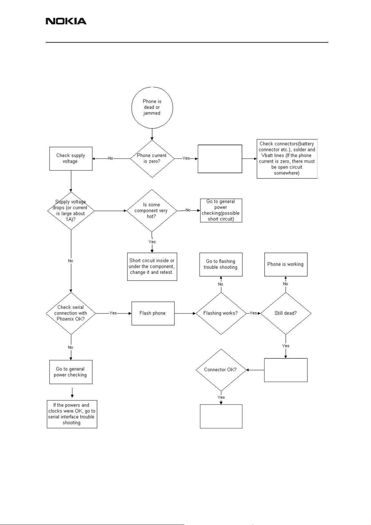
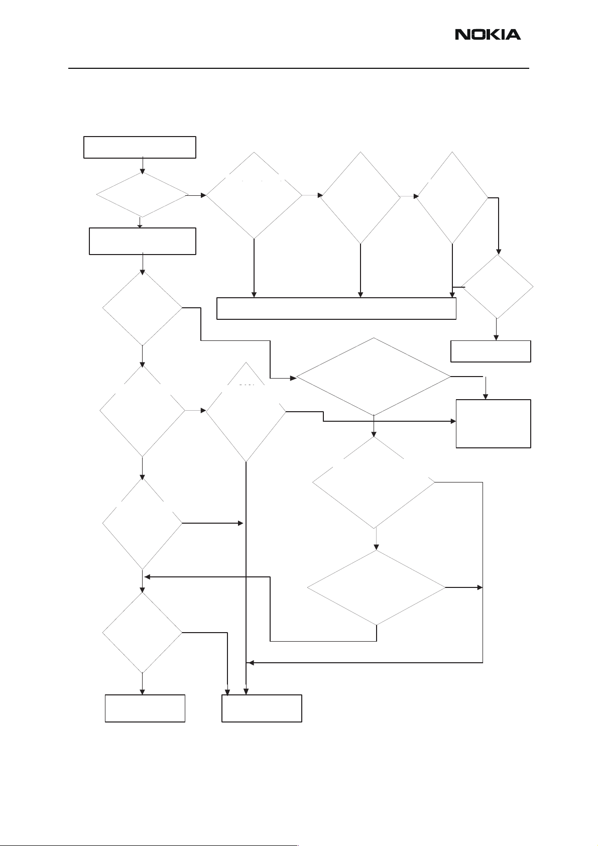
Troubleshooting Paths
Dead or jammed device
Disassemble
Check UI
connector
display
Replace
UI module
display
Issue 2 09/2004 Copyright © 2004 Nokia Corporation Page 6-7
Company Confidential
Page 8

NEM-4 Company Confidential
6 - Troublehsooting Instructions Nokia Customer Care
Partially damaged device
If the device is working, but some functionality is missing try to localize where the problems is and see relevant part of this manual. E.g audio is not working see “Audio Troubleshooting” , if charging is not working see chapter Charging Troubleshooting etc.
Most common symptoms reported by customer
In this chapter is described most common symptoms reported by customers when the
device is brought in for service. Some tips where the trouble can be found are given also.
When Troubleshooting use these tips and follow the given Troubleshooting path.
Most common symptoms for audio problems
“Earpiece sound is missing”
”Headset is not recognized”
”Microphone is not working”
”Volume cannot be adjusted”
”Ringing tones does not work”
”Audio volume too low”
“Radio does not work”
“IHF sound is missing”
“Headset sound is missing”
“MP3/AAC play does not work”
If the symptom is something like above, see audio Troubleshooting.
Most common symptoms for USB and BT problems
“Bluetooth does not work or a connection can not be established”
“USB connection does not work or PC cannot find device”
If symptoms are something like above, follow USB or Bluetooth Troubleshooting guidelines.
Symptoms related to energy management
“Phone does not stay on”
”Charging is not working”
”Time is lost during battery change”
”Charging takes too long”
”Operating time is very short”
Page 6-8 Copyright © 2004 Nokia Corporation Issue 2 09/2004
Company Confidential
Page 9
Company Confidential NEM-4
Nokia Customer Care 6 - Troublehsooting Instructions
These symptoms lead to relevant part of energy management Troubleshooting
Problems related to UI:
“Keypad is not working”
”Backlight is dim”
”Backlight not even”
”Backlight is blinking”
”Keypad or display backlight is not working”
”Display related problems”
“Rocker is not working”
Most common RF related symptoms:
“Call cannot be made”
”Phone does not find signal”
”Call is often dropped”
See RF Troubleshooting.
ASIC is changed
ASIC’s can be changed only at a defined service level.
UEM changed
If UEM is changed baseband calibrations should be made. New IMEI must be programmed also. ZOCUS calibration is not necessary.
UPP_WD2 changed
IMEI must be reprogrammed.
ZOCUS changed
Zocus must be re-calibrated
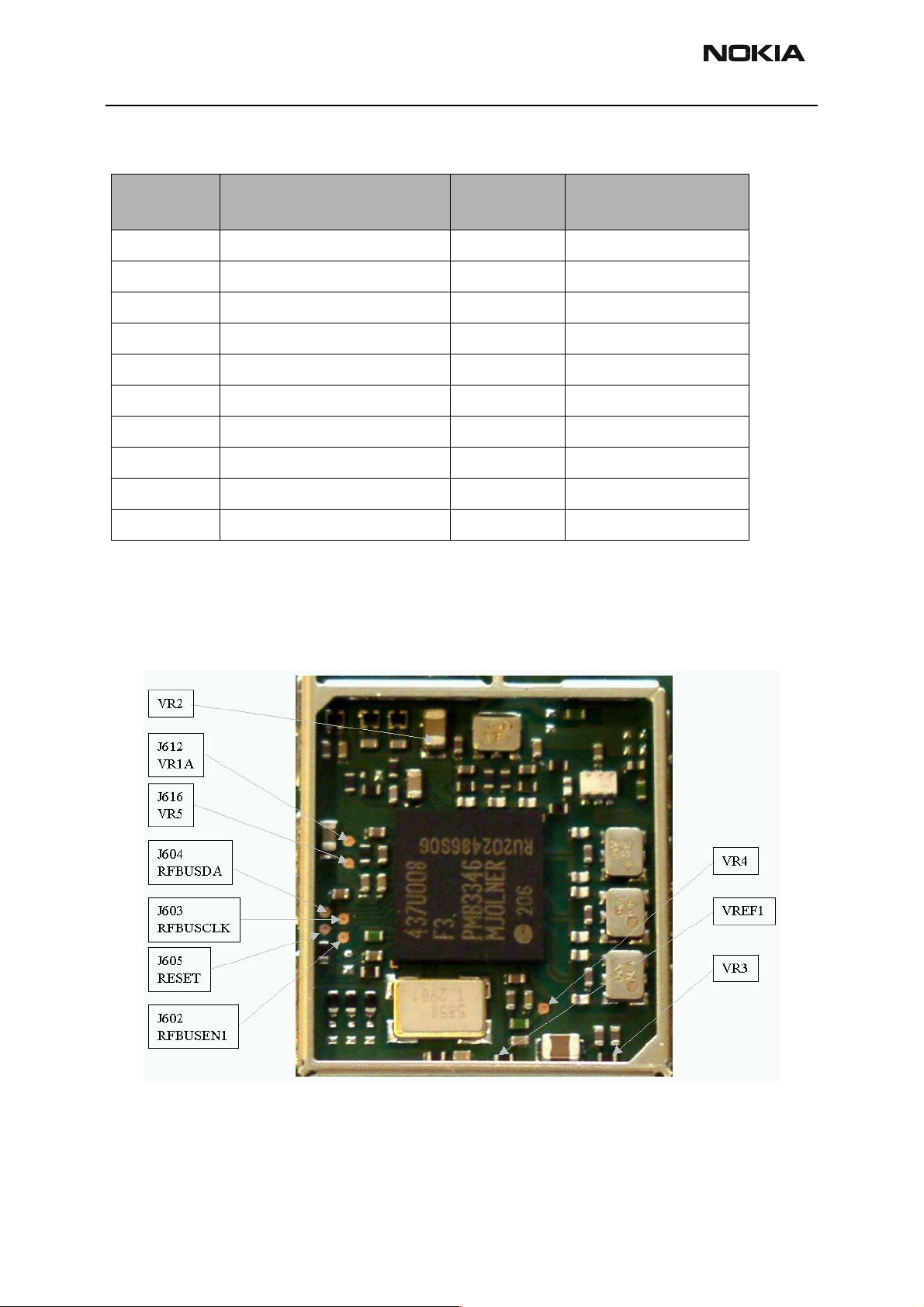
Test points
Test
Point
J128 GPIO1 (WD2->ADSP)
Signal description
Table 1: Test points in Baseband area
J129 GPIO0 (ADSP->WD2)
J904 VCOREA enable (N261 EN, UEMRST)
J900 VHPA enable (N266 EN, GENIO14)
J901 VAUD (N265 EN, GENIO25)
J903 VAUX2 enable (N264 EN, GENIO16)
J218 GENTest0
Issue 2 09/2004 Copyright © 2004 Nokia Corporation Page 6-9
Company Confidential
Page 10
NEM-4 Company Confidential
6 - Troublehsooting Instructions Nokia Customer Care
Test
Point
J004 N330 (Boomer) _SHUTDOWN (from WD2 GENIO8)
J906 ADSP S11 (WD2->ADSP through UEM level shifter
J907 ADSP S13 (ADSP->WD2 through UEM level shifter
J558 ADSP CLKR0 (BCLK_OUT) to AIC
J559 ADSP DR0 (DIGITAL_AUDIO_IN) from AIC
J560 ADSPDX0 (DIGITAL_AUDIO_OUT) to AIC
J561 ADSP FSX0 (LRC_OUT) to AIC
J562 ADSP C1 (ADSP Flash OE#)
J563 ADSP C2 (ADSP Flash WE#)
J567 ADSP C3 (ADSP Flash CE1#)
J312 FLASH _CE (D310)
J315 FLASH CLK (D310, D311, D313)
Signal description
IRLEDC)
IRRXN)
J311 FLASH _CE (D311)
J313 FLASH _CE (D313)
J197 GPIO13 (Keyboard matrix ROW0)
J196 GPIO12 (Keyboard matrix ROW1)
J179 GPIO16 (Keyboard matrix COL4)
J116 GPIO30 (Keyboard matrix COL5)
J119 GPIO15 (Keyboard matrix ROW3)
J118 GPIO14 (Keyboard matrix ROW2)
J176 GPIO18 (Keyboard matrix ROW5)
J175 GPIO17 (Keyboard matrix ROW4)
J177 GPIO10 (Keyboard matrix COL2)
J178 GPIO11 (Keyboard matrix COL3)
J117 GPIO8 (Keyboard matrix COL0)
J180 GPIO9 (Keyboard matrix COL1)
J181 GENIO1 (ROCKER1)
J145 GENIO2 (ROCKER2)
J182 GENIO10 (ROCKER3)
J194 GENIO28 (MUSIC PL KEY)
J184 GENIO11 (ROCKER5)
Page 6-10 Copyright © 2004 Nokia Corporation Issue 2 09/2004
Company Confidential
Page 11
Company Confidential NEM-4
Nokia Customer Care 6 - Troublehsooting Instructions
Test
Point
J183 GENIO13 (ROCKER4)
J912 LCD signal
J185 LCD signal
J186 LCD signal
J187 LCD signal
J188 LCD signal
J189 LCD signal
J190 LCD signal
J191 LCD signal
J113 LCD signal
J114 LCD signal
J905 UEM DLIGHT (Display LED driver control)
J404 SIM Data
Signal description
J405 SIM Clock
J406 SIM Reset
J913 MMC CMD
J914 MMCDAT0
J577 N470 Dir3
J579 N470 Dir2
J576 N470 A1
J578 N470 A3
J593 N470 A2
J910 N470 EN2
J911 N470 EN1
J568 USB PU ?
J569 USB D+
J575 USB D-
J398 VBAT (After current sense monitor) R382
J902 N301Zint
Issue 2 09/2004 Copyright © 2004 Nokia Corporation Page 6-11
Company Confidential
Page 12
NEM-4 Company Confidential
6 - Troublehsooting Instructions Nokia Customer Care
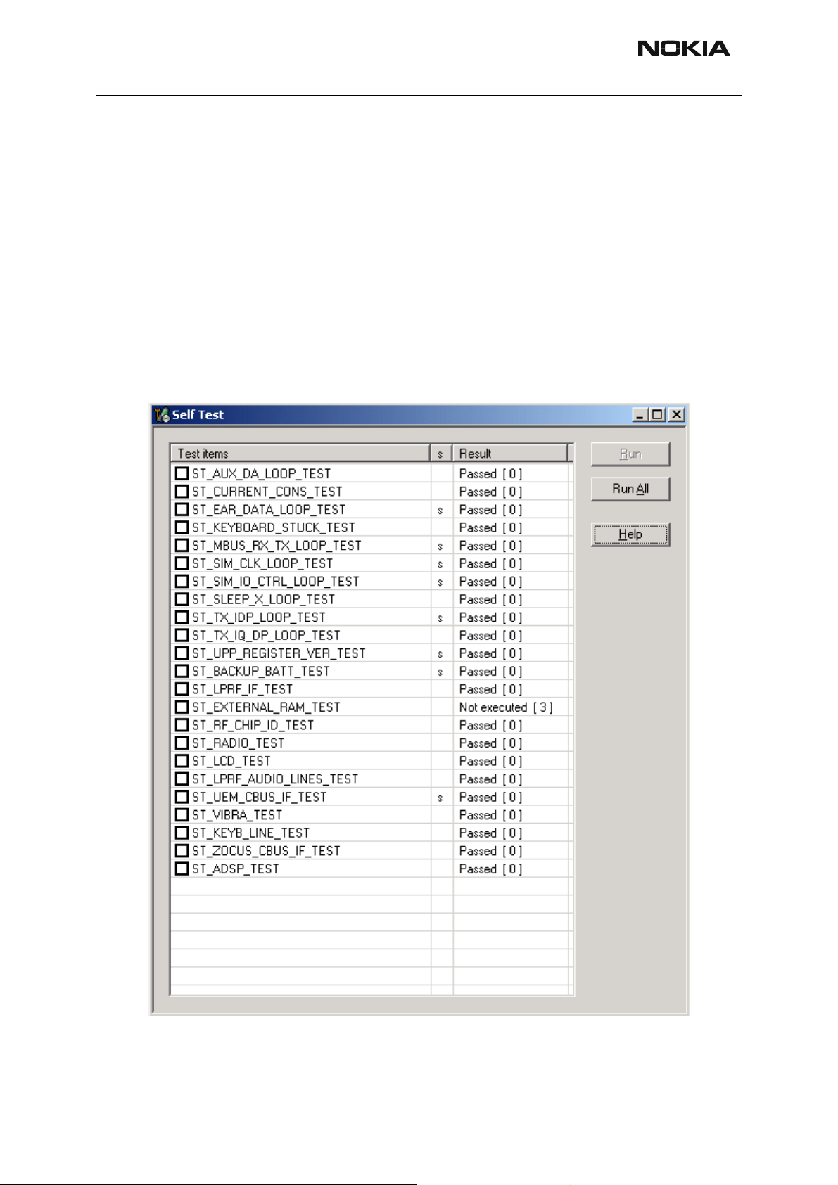
“CONTACT SERVICE” on display
CONTACT SERVICE on display (Self-tests by Phoenix)
Display information: “Contact Service”
This fault means that software is able to run and thus the watchdog of UEM can be
served.
Selftest functions are executed when the phone is powered on and if one or more selftest functions fail, the message “Contact Service” is shown on the display.
MCU selftest cases can be split into two categories: The ones that are executed during
power up and the ones that are executed only with a PC connected. These test and the
items included are as follows:
If some selftest is failed, see relevant chapter in this Troubleshooting document.
Page 6-12 Copyright © 2004 Nokia Corporation Issue 2 09/2004
Company Confidential
Page 13
Company Confidential NEM-4
Nokia Customer Care 6 - Troublehsooting Instructions
Baseband HW Subarea Troubleshooting
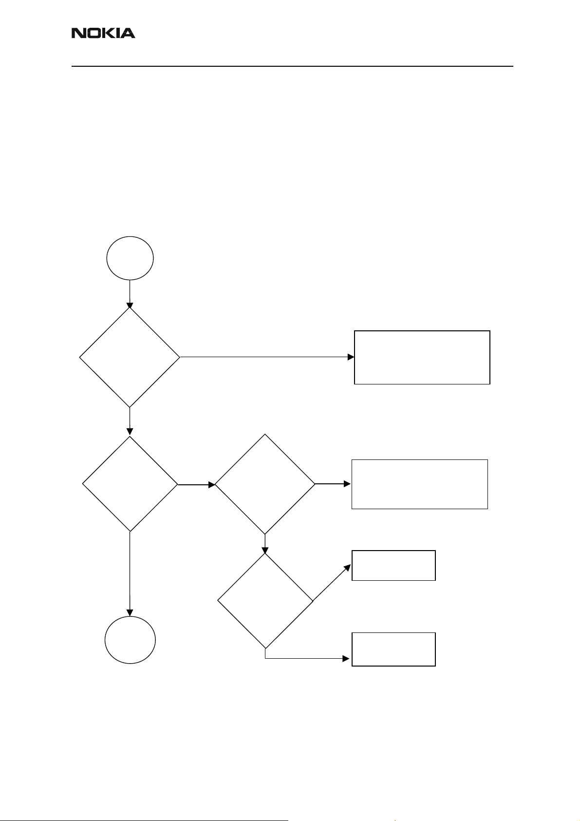
Flashing troubleshooting
NEM-4 has three memory components installed on the main pwb. The best indication of
which one is causing problems can be obtained by flashing the device. It has to be kept
in mind that all three flashes are interfaced with UPP WD2 asic that might it self have
some problems. The necessary steps are described below. Phoenix error messages during
flashing greatly help on defining what is wrong. To be able to flash the device, most
device BB area components must function properly.
Flashing
faults
The phone does
not set Flashbus
TXD line high
after startup
No
The phone does
not set the
flashbus TXD
line low after the
startup
No
Memory
faults page
2
Yes
Yes
Measure BSI
pulse during
flash
programming
Is it ok?
Yes
Measure
FBUSTX line
during flash
programming is
it 1.8V?
Yes
No
No
Check connections
Check BB voltages
Check clocks
Change UEM
Check BSI line
Check BSI line
Battery connector, flex,
Battery connector,
C239, Z383, R384
C226, R220 and R385
Change
UEM
Change UPP
WD2
Issue 2 09/2004 Copyright © 2004 Nokia Corporation Page 6-13
Company Confidential
Page 14
NEM-4 Company Confidential
g
6 - Troublehsooting Instructions Nokia Customer Care
Memory
faults
page2
"Secondary
receive fail" or
"Algorithm send
failed"
messa
Prommer
message about
sdram failure?
manufacturer ID
and device ID
e?
No
No
Wrong
No
Yes
Yes
Yes
Change UPP_WD2
Activity in SDRAM
Activity in sdram
Clk J314 pad?
clk J108 pad?
No
Change UPP_WD2
Change Flash Chip
according to Phoenix
messages
If both chips report wrong
ID's -> change UPP_WD2
Yes
Change SDRAM
Yes
Voltages
Voltages
VmemA and
VmemA and
Vio OK?
VioA ok?
No
EM
troubles
"Flash informs
about a failure"
during flashing
No
Retest
ADSP Flashing
Yes
Check flash0 bypass caps, check
Vpp connection to flasher, Check
Vpp resistor(4.7k)
Vpp resistor (R314, 4.7k)
Ok->Change flash0
Page 6-14 Copyright © 2004 Nokia Corporation Issue 2 09/2004
Company Confidential
Page 15
Company Confidential NEM-4
Nokia Customer Care 6 - Troublehsooting Instructions
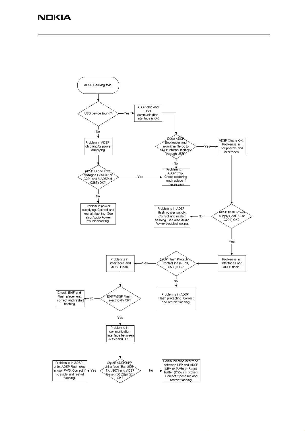
ADSP flashing troubleshooting
ADSP flash environment consists of ADSP, ADSP flash, EMIF (external memory interface),
communication interfaces (USB and UPP/UEM), ADSP flash protecting control and power
supplies for ADSP and ADSP flash.
Issue 2 09/2004 Copyright © 2004 Nokia Corporation Page 6-15
Company Confidential
Page 16

NEM-4 Company Confidential
6 - Troublehsooting Instructions Nokia Customer Care
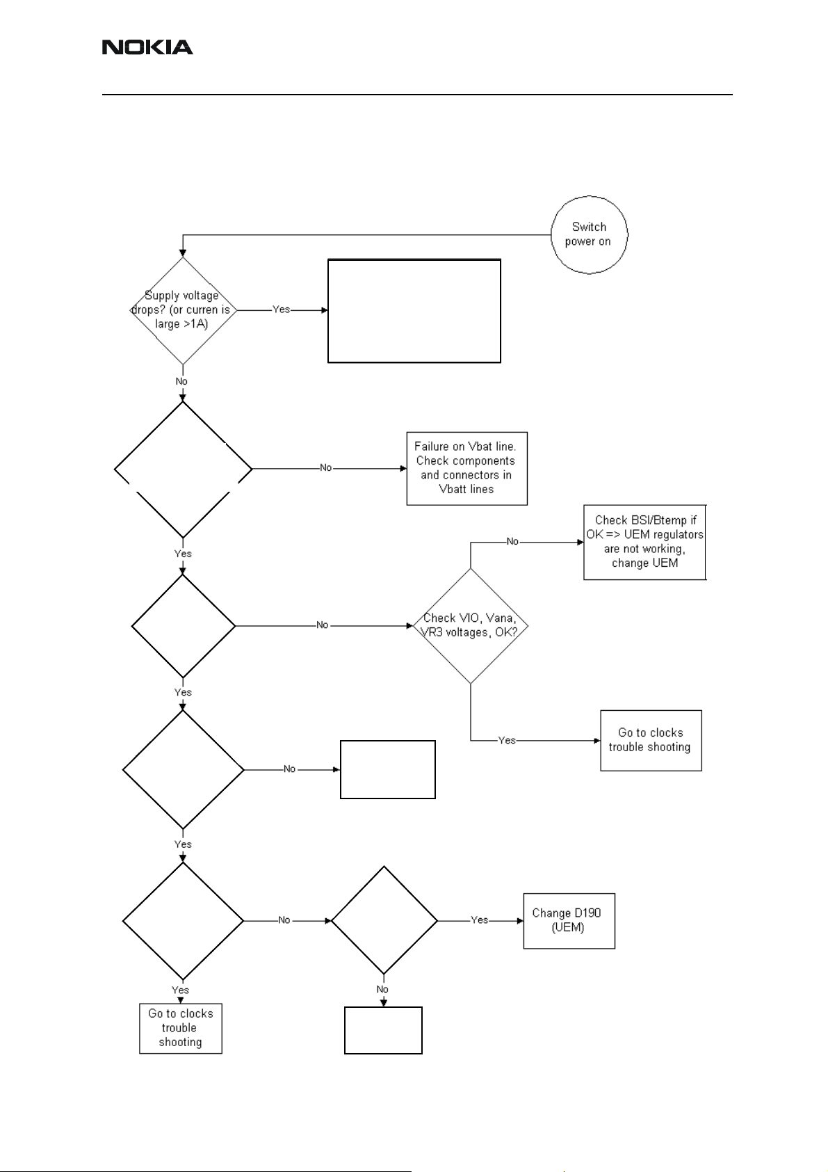
Energy management troubleshooting
Device does not stay on
If the device is switched off without any visible reason, there may be problems in the following areas:
• UEM watchdog problem (WD is not updated by SW)
• BSI line problem (BSI line is floating => contact failure)
• Battery line problem
• Soldering problem
The most likely reason is UEM WD (watchdog), which turns the device off after about 32
seconds if SW is jammed.
This may caused by SW problem, UPP_WD2 problem (Not server by SW), UEM or memory
malfunctions.
The following tests are recommended:
• General power checking
• Clocks
•Memory testing
• Serial Interface
If there is something wrong in BSI line, the device seems to be dead after the power key
is pressed. However the regulators of the device are on a few seconds before the powerdown.
This mode can easily be detected from the current consumption of the device. After a
few seconds the current consumption drops almost to 0 mA.
In this case check component or soldering
• Battery connector X381
EMI-filter R385
UEM D190 (pin number C2)
If phone boots to TEST or LOCAL mode with normal battery, BSI is short circuited to
ground. Check EMI-filter and filtering capacitors, which are located to BSI.
Page 6-16 Copyright © 2004 Nokia Corporation Issue 2 09/2004
Company Confidential
Page 17
Company Confidential NEM-4
(
)
(
)
Nokia Customer Care 6 - Troublehsooting Instructions
General power checking
Use service tool FLA-41R. Battery voltage should be at least 3.6V. After phone disassembly, use module jig MJS-8Q.
Short circuit in Vbatt1-3,
VBATHF or BT voltage lines. Try to
Vbattbb or Vbattihf lines. Try to
find short circuit. Check
components which are able to
short cuircuit these lines,
(filtering components etc.)
Vbatt1-3, Vbatbb,
BT voltage meas.
Vbattihf meas. from
C301, C302 & C313
VBATHF,
R433
PURX (J125)
1.8V?
Check Vcorea
and Vmema
voltages, OK?
See next page
Check sleep
J123
clock (J124)
32.768Khz?
Meas. from
C197, OK?
Check B190,
C196, C197
Issue 2 09/2004 Copyright © 2004 Nokia Corporation Page 6-17
Company Confidential
Page 18
NEM-4 Company Confidential
6 - Troublehsooting Instructions Nokia Customer Care
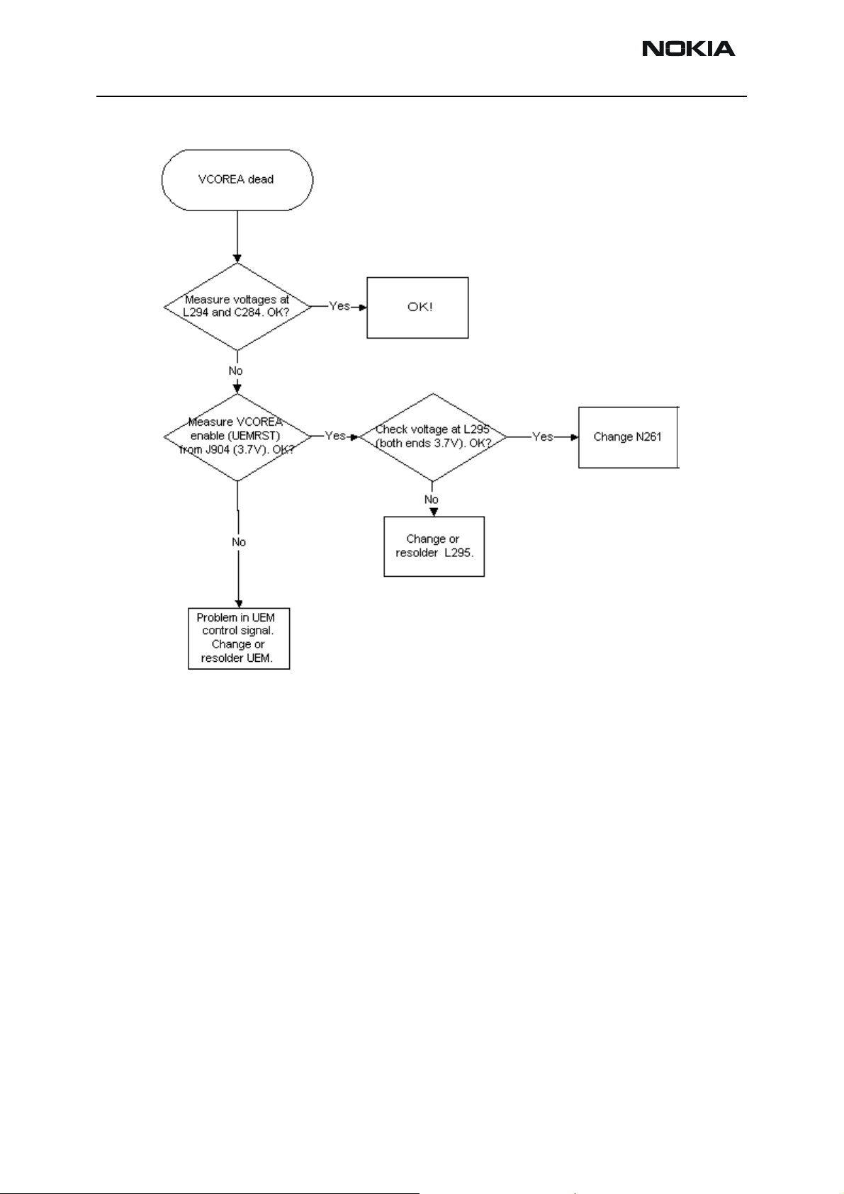
VCOREA troubleshooting
Page 6-18 Copyright © 2004 Nokia Corporation Issue 2 09/2004
Company Confidential
Page 19
Company Confidential NEM-4
Nokia Customer Care 6 - Troublehsooting Instructions
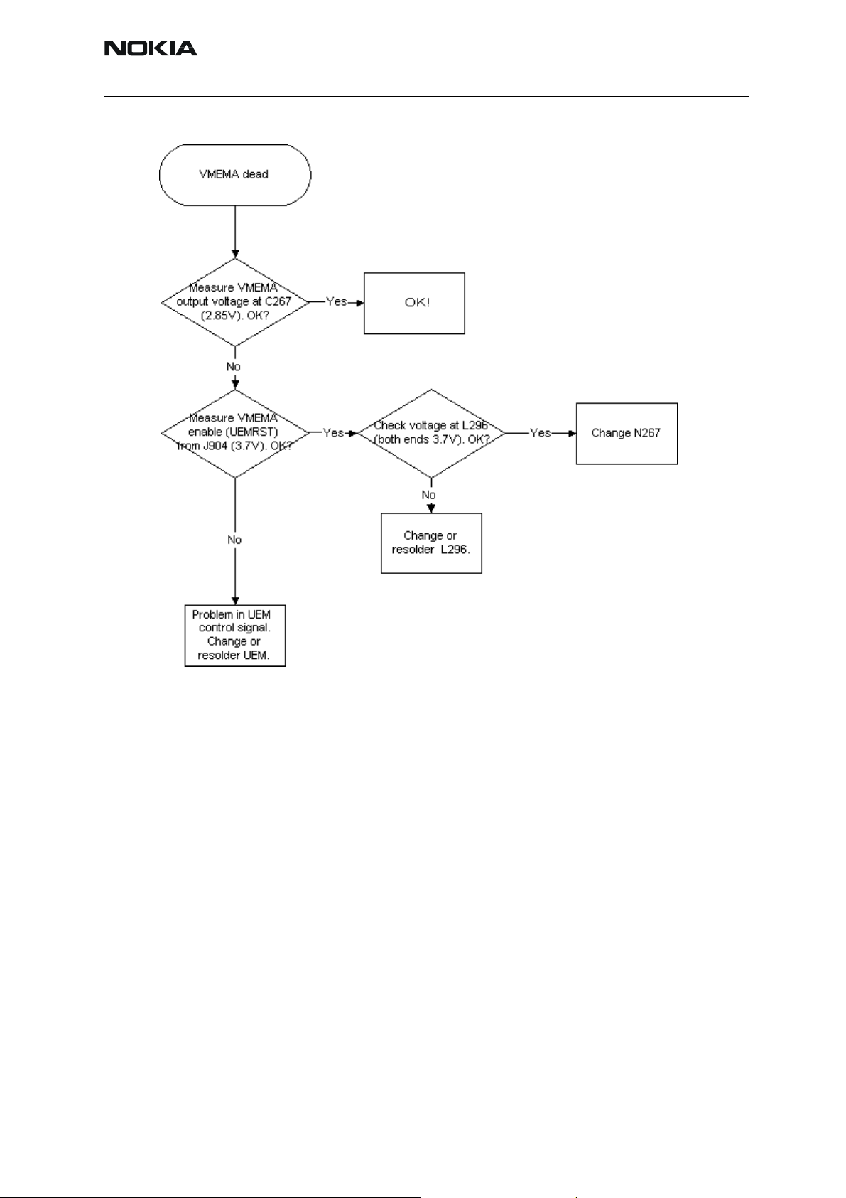
VMEMA troubleshooting
Issue 2 09/2004 Copyright © 2004 Nokia Corporation Page 6-19
Company Confidential
Page 20
NEM-4 Company Confidential
6 - Troublehsooting Instructions Nokia Customer Care
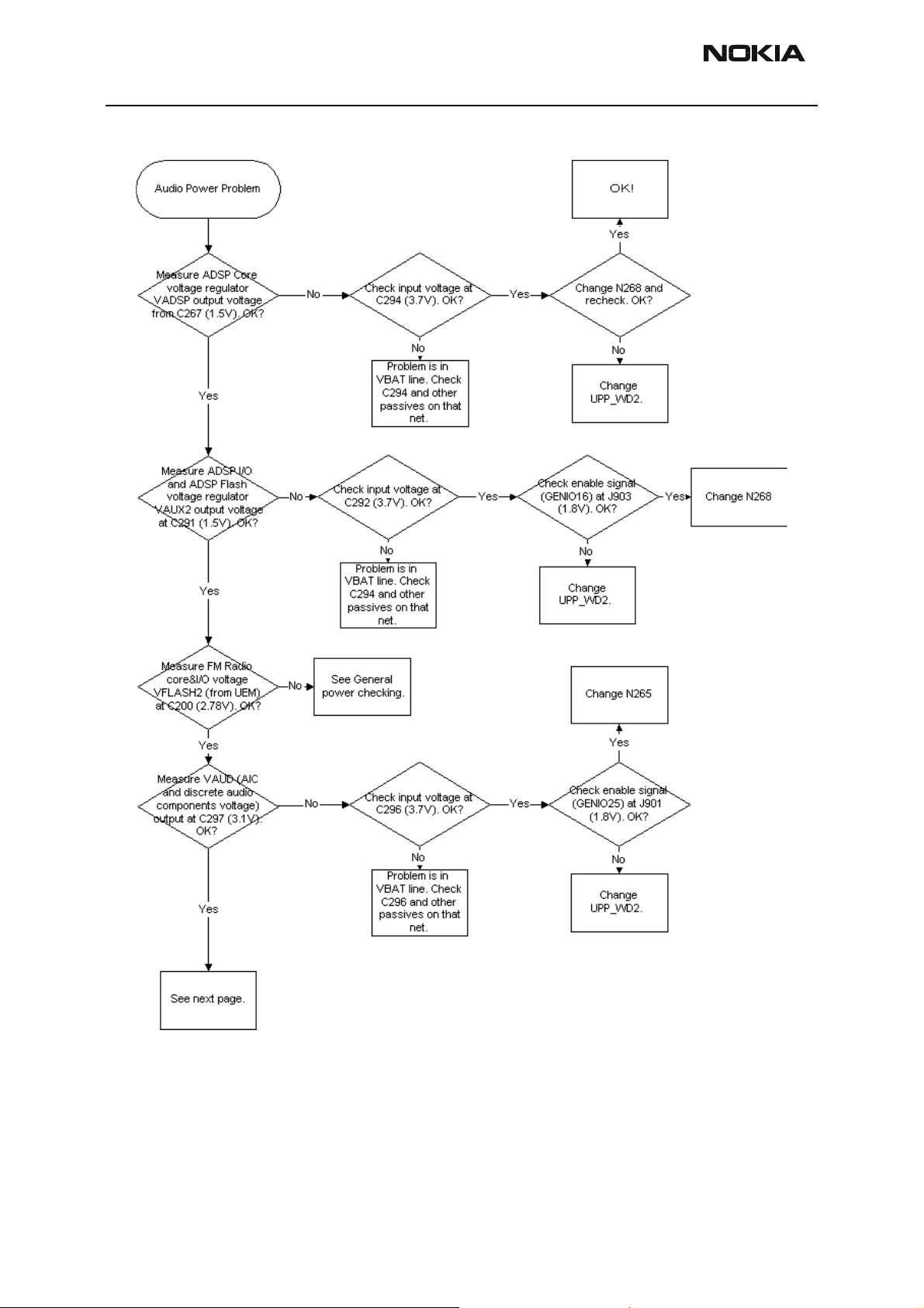
Audio power troubleshooting
Page 6-20 Copyright © 2004 Nokia Corporation Issue 2 09/2004
Company Confidential
Page 21
Company Confidential NEM-4
Nokia Customer Care 6 - Troublehsooting Instructions
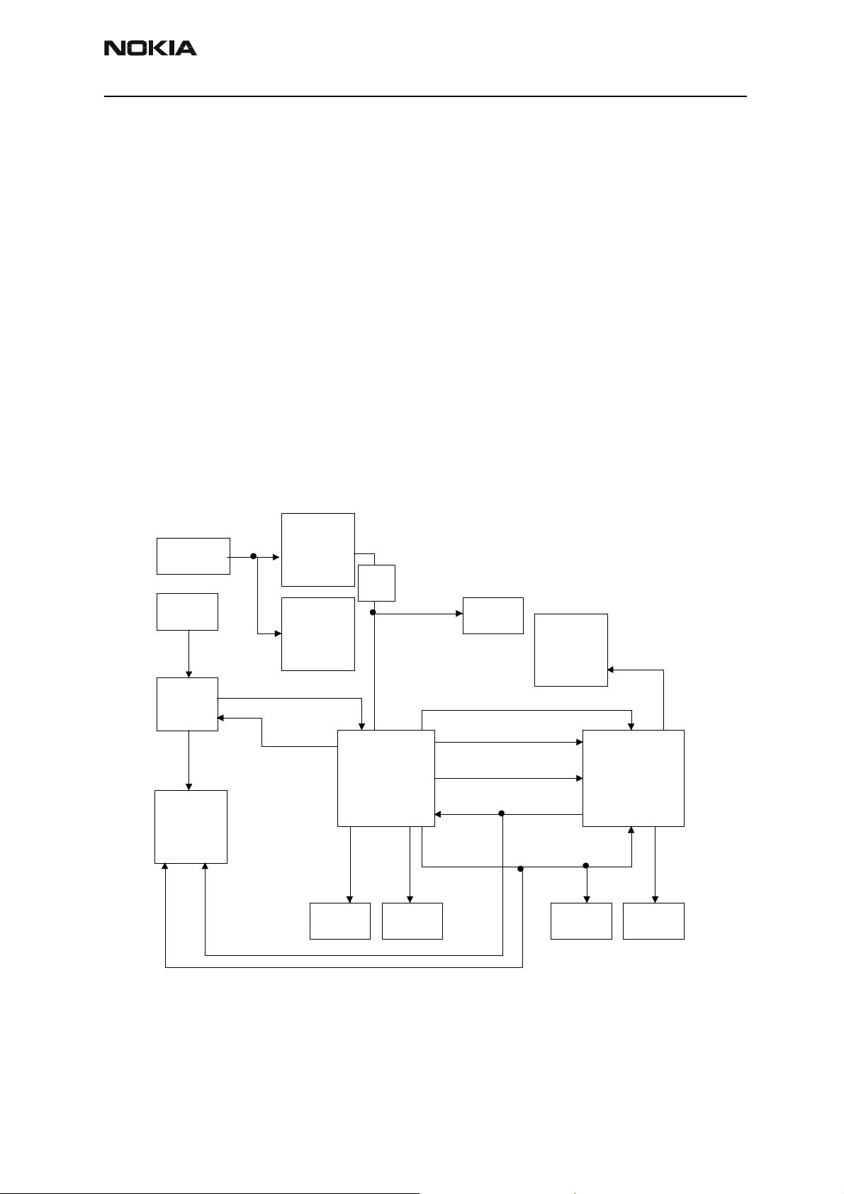
Clocks troubleshooting
Clocks include the following:
RF-clock
ADSP Clock
DBUS, CBUS clocks
Flash and SDRAM clocks
Sleep clock
Bluetooth clock
SIM clock
MMC clock
NEM-4 has three external oscillators for baseband clocking. The main clock is generated
by 26MHz oscillator (B601) and routed through Mjoelner RF ASIC to UPP_WD2 engine
ASIC. Sleep Clock is generated by 32kHz oscillator to UEM, which then supplies it to
UPP_WD2, Bluetooth module and FM radio chip. The third oscillator generates 12MHz
clock for ADSP and AIC. UPP_WD2 uses the system clock to generate various clocks for
different purposes
12MHz
Oscillator
VCXO
26MHz
Mjoelner
SysClk
Bluetooth
Audio
Clock
Amadeus
Audio
Codec
RFClk
RFBusClk
Figure 1: Clock diagram.
Buffer
MMC Clock
UPPWD2 UEM
SDRClk
Flash
Clock
MMC
RFConvClock
SIM Clock
DBus Clock
Sleep Clock
Nectar
CBus Clock
FM Clock
SIM
Clock
SDRAM
SIMZocusFlash
System clock can be measured from the lower pad of capacitor C171. This clock should
be running when phone is on.
In SLEEP mode the VCXO is off. UEM generates low frequency clock signal (32.768 kHz)
that is fed to UPP_WD2, Bluetooth and ZOCUS.
Issue 2 09/2004 Copyright © 2004 Nokia Corporation Page 6-21
Company Confidential
Page 22
NEM-4 Company Confidential
6 - Troublehsooting Instructions Nokia Customer Care
When the flashing of the device does not succeed, but powering is OK, follow these
instructions.
Note: The absence of clocks may indicate that the device (put phone to LOCAL mode
when the sleep is not allowed or press buttons so that phone is not in sleep mode) is in
sleep mode. Make sure that the device is not in sleep during clocks measuring.
IMPORTANT: Clock signals have to be measured with 1MΩ (or greater) probes!
Measure signal from J170. This should be 26Mhz clock signal. See RF Troubleshooting for
further information.
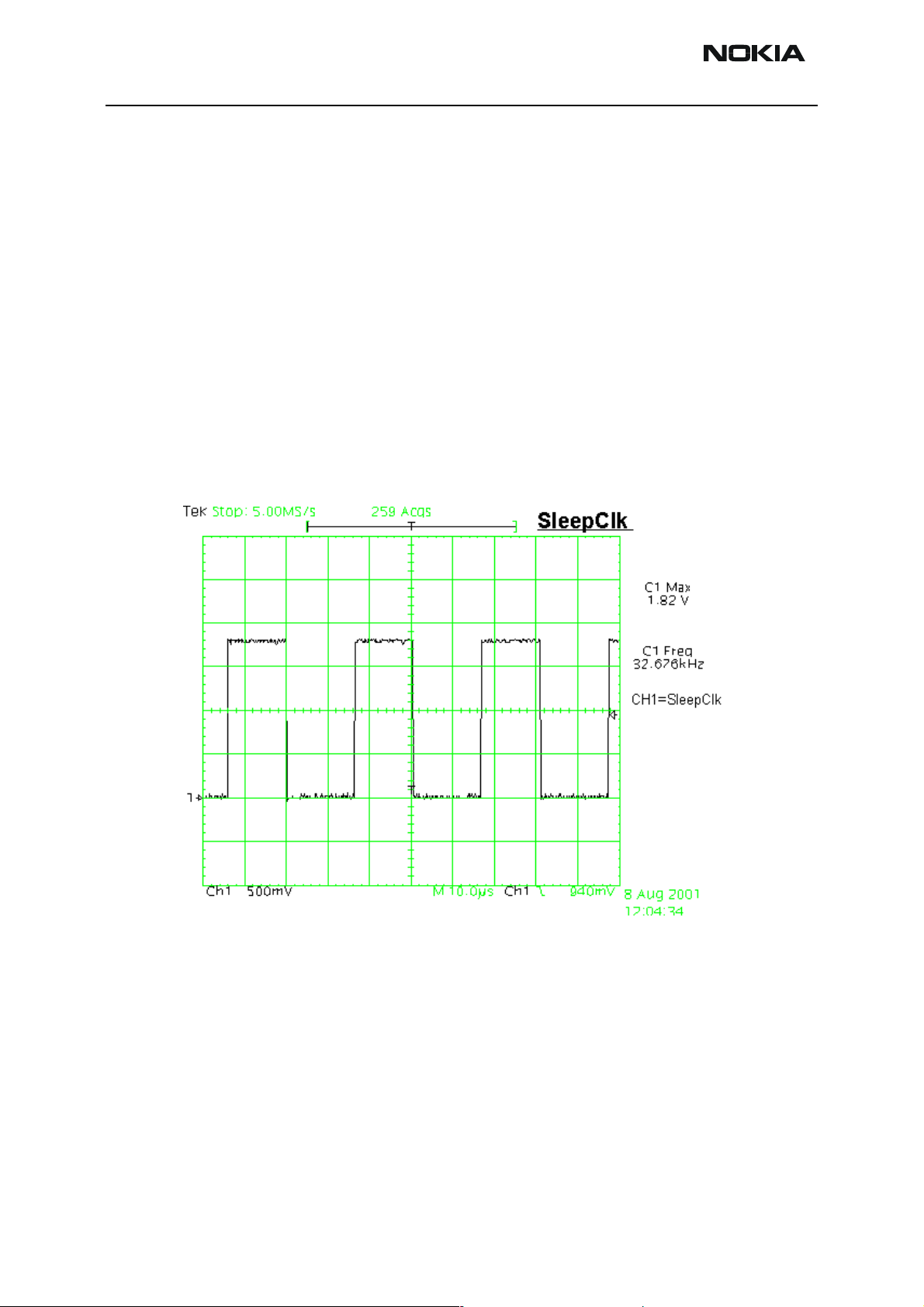
Check the crystal oscillator (B190) is oscillating at 32.768kHz frequency. If not change
B190. If ok, measure SleepClk from test point from capacitor C521. Frequency should be
the same 32.678kHz (see Figure 2, “Sleep clock,” on page 22 below.) If not change UEM.
Figure 2: Sleep clock
ADSP Clock (12MHz sine wave) can be measured from oscillator B550.
Charging checking
Use the BL5-C battery and JBV-1/MJF-26 calibration set to test charging. (NOTE: power
supply cannot be charged if it not has a current sinking capability.) When you are charging totally empty battery, remember that start-up charging might take a little bit longer
time than normal. During this time display is blank.
If charger is not NMP approved type and its current and voltage is not within NMP
charger window then software does not start charging and there is “NOT CHARGING” on
the display. Voltage should be between 5.3V - 9.5V and current between 200mA –
(Capacitor C521)
(Testpoint J124)
Page 6-22 Copyright © 2004 Nokia Corporation Issue 2 09/2004
Company Confidential
Page 23

Company Confidential NEM-4
Nokia Customer Care 6 - Troublehsooting Instructions
900mA
Remove and reconnect battery and charger few times before you start to measure
device. This check ensures that the fault really exists.
(Refer to “Charging Troubleshooting”)
Issue 2 09/2004 Copyright © 2004 Nokia Corporation Page 6-23
Company Confidential
Page 24
NEM-4 Company Confidential
6 - Troublehsooting Instructions Nokia Customer Care
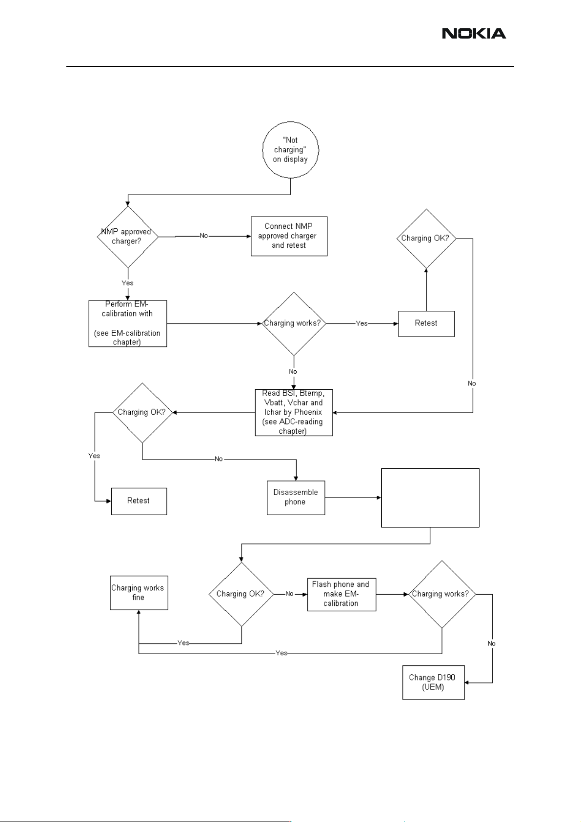
Figure 3: Charging Troubleshooting
Phoenix and JBV1/MJF26
Check BL5-C, Btemp, BSI,
X606, R385, R404
X381,
Page 6-24 Copyright © 2004 Nokia Corporation Issue 2 09/2004
Company Confidential
Page 25
Company Confidential NEM-4
Nokia Customer Care 6 - Troublehsooting Instructions
Nothing
happens
ACP-12
when ACP-2
is connected
Measure Vchar
at C384. Is it
at C388 and C387. Is it
>3.0Vdc?
Replace
Replace R191
R190/Z190 and
and retest
retest.
F381,
Check F380, TVS,
V383 and L381.
V381 and L380
Check R191
Check R191,
and Z190.
is it OK?
Are they ok?
Issue 2 09/2004 Copyright © 2004 Nokia Corporation Page 6-25
Company Confidential
Page 26
NEM-4 Company Confidential
6 - Troublehsooting Instructions Nokia Customer Care
Energy management calibration
During energy management calibration A/D-converter, BSI, Btemp, Battery voltage,
Charger voltage and Charger current are calibrated.
Limits for calculated calibration values are as follows:
Channel Low High
ADC Offset -50 50
ADC Gain 26000 29500
BSI Gain 860 1180
Vbatt Offset 2400 2600
Vbatt Gain 10000 11000
Vchar 57000 63000
Ichar 3600 5000
ADC-offset over limits:
Inspect BSI line and components in it (R385, Pull-up resistor R220). If these are OK,
change UEM.
BSI Gain over limits:
Inspect BSI line and components in it (R385, Pull-up resistor R220). If these are OK,
change UEM.
Page 6-26 Copyright © 2004 Nokia Corporation Issue 2 09/2004
Company Confidential
Page 27
Company Confidential NEM-4
Nokia Customer Care 6 - Troublehsooting Instructions
Vbatt offset and Gain:
Inspect Vbatt lines and component in it.
Vchar over limits:
Inspect components which are connected Vchar line: V383, F381 and L381
Ichar over limits:
Inspect components which are connected at Vchar line. If those are OK, First change
current sense resistor (R191), if calibration is not still successful change UEM.
Calibration can be checked using ADC-readings. Known voltages, currents and resistances are fed and read by ADC-readings, read values and known values can be compared.
ADC-reading
Divided and scaled battery voltage, Charger voltage, Charger current, BSI and Btemp values can be read by this tool. Read values few times before you can be sure that results
are accurate.
NOTE: IF Vbatt Scaled and Divided unit results are different default calibration values are
used. In this case perform EM-calibration to get full performance of phone.
Issue 2 09/2004 Copyright © 2004 Nokia Corporation Page 6-27
Company Confidential
Page 28
NEM-4 Company Confidential
6 - Troublehsooting Instructions Nokia Customer Care
Maximum tolerances are:
Reading Check point Tolerance
Reading Check point Tolerance
Vbatt SCAL
Vchar 8.4V ± 40mV
Ichar 500mA ± 20mA
BSI 75k ± 1.3kohm
Btemp 273K(47k) ± 5K
4.2V ± 25mV
Backup battery
Symptom of backup battery fault is
Real Time Clock loses the correct time during short main battery removal.
The same symptom can also be seen when the backup battery is empty. About 30 minutes is needed to fully charge the backup battery in the device. NOTE: Backup battery is
charged when the phone is powered or when the device is LOCAL or TEST mode.
Always check the backup battery visually for any leakage or any other visual defect.
Check that the backup battery is correctly mounted in the device before closing the
cover.
Check with Phoenix that backup battery is OK
Measure the voltage of backup battery
• Normal operation when the voltage is > 2.0V
• Fully charged when the voltage is about 3.2V (because of large internal impedance voltage won’t stay above 3.0V a long time after charging is disabled)
Enable backup battery charging (start to charge main battery or boot device to LOCAL or
TEST mode)
Measure voltage of backup battery during charging, It should arise if it is not 3.2V, yet.
When the voltage is over 2.0V for sure, check backup battery with Phoenix.
-> In not OK then D190 is faulty.
Ensure that the RTC is running.
Page 6-28 Copyright © 2004 Nokia Corporation Issue 2 09/2004
Company Confidential
Page 29
Company Confidential NEM-4
Nokia Customer Care 6 - Troublehsooting Instructions
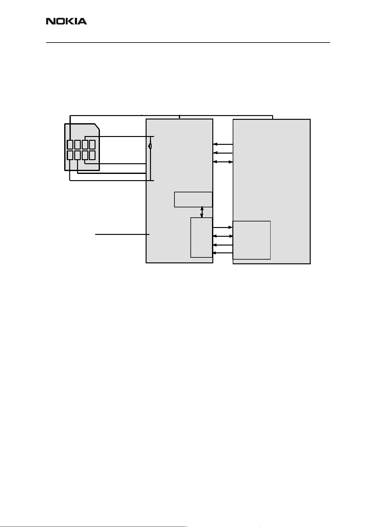
SIM card
The whole SIM interface locates in two chips UPP_WD2 and UEM. UEM contains the SIM
interface logic level shifting. UPP provides SIMClk through UEM to the SIM. SIM interface supports both 3 V and 1.8 V SIMs.
UPP & UEM SIM connections
GND
UPP
SIM
C5 C6 C7
C1C2C3
BSI line from battery
SIMCLK
SIMRST
SIMDATA
VSIM
BSI
GND
UEM
SIMIF
register
SIMIO
SIMClk
Data
UEM
digital
logic
SIMIO
SIMClk
Data
UIF Block
UEMInt
CBusDa
CBusEnX
CBusClk
The SIM power up/down sequence is generated in the UEM. This means that the UEM
generates the RST signal to the SIM. Also the SIMCardDet signal is connected to UEM.
The card detection is taken from the BSI signal, which detects the removal of the battery.
Monitoring of the BSI signal is done by a comparator inside UEM. The threshold voltage
is calculated from the battery size specifications.
The SIM interface is powered up when the SIMCardDet signal indicates ”card in”. This
signal is derived from the BSI signal. SW tries first to power up the SIM with 1.8 V. If this
doesn't succeed power up is repeated with VSIM switched to 3 V.
The data communication between the card and the phone is asynchronous half duplex.
The clock supplied to the card is in GSM system 1.083 MHz or 3.25 MHz. The data
baudrate is SIM card clock frequency divided by 372 (by default), 64, 32 or 16.
Issue 2 09/2004 Copyright © 2004 Nokia Corporation Page 6-29
Company Confidential
Page 30
NEM-4 Company Confidential
6 - Troublehsooting Instructions Nokia Customer Care
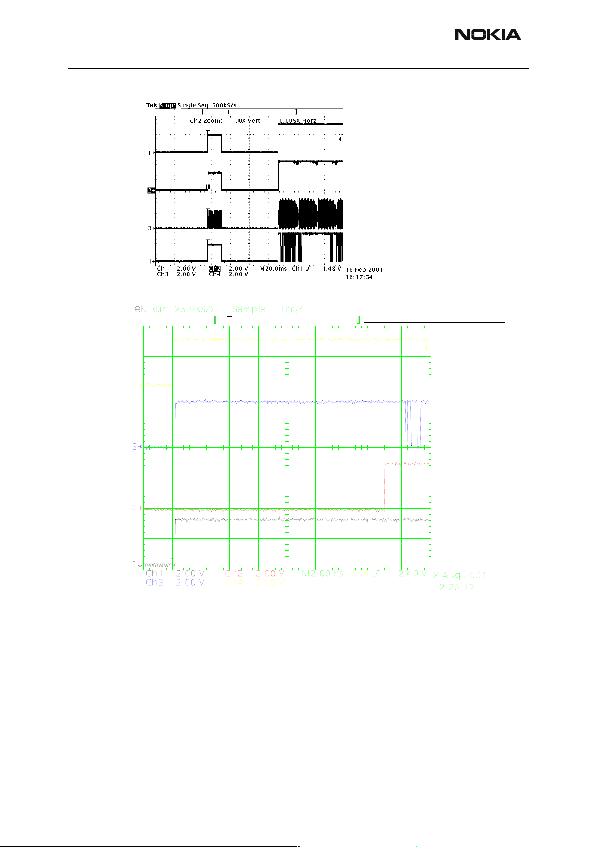
Figure 4: SIM Power Up.
Ch1 Vsim
Ch2 Reset
Ch3 Clock
Ch4 I/O
Measured with
3Vsim
Figure 5: SIM answer to reset.
SIM answer to reset
CH1 = SIM_CLK
CH2 = SIM_RST
CH3 = SIM_I/O
CH4 = SIM_PWR
Measure points
SIM connector
Page 6-30 Copyright © 2004 Nokia Corporation Issue 2 09/2004
Company Confidential
Page 31
Company Confidential NEM-4
Nokia Customer Care 6 - Troublehsooting Instructions
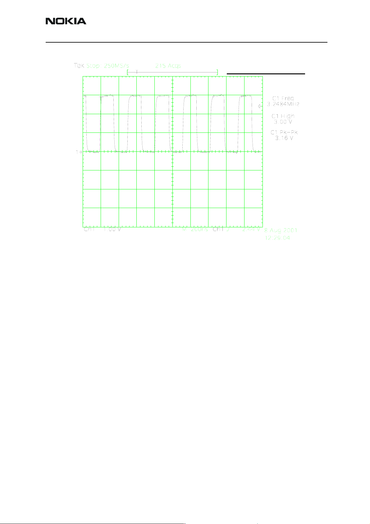
Figure 6: SIM Clk 3.25MHz.
SIM_Clk_3.25MHz
CH1 = SIM_CLK
Measure points
SIM connector
Remember to check the two PHOENIX test cases before changing UPP!!!!
Issue 2 09/2004 Copyright © 2004 Nokia Corporation Page 6-31
Company Confidential
Page 32
NEM-4 Company Confidential
Ch
VSIM
d
6 - Troublehsooting Instructions Nokia Customer Care
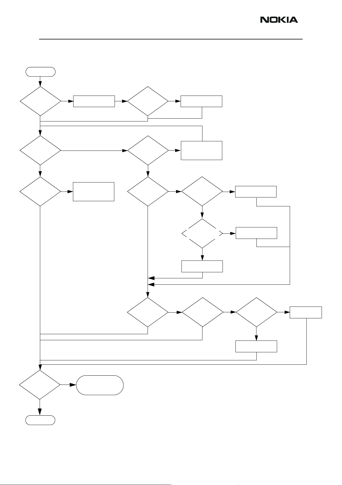
"Insert SIM Card" in device display although card is inserted
START
Perform
SIM BB self tests.
Are they OK?
Yes
Perform
Phoenix SIM tests.
Are they OK?
Yes
Is the SIM
Detection Reliable?
Yes
No
Check & clean battery
centre contact. Verify BSI
signal has a steady voltage.
Replace UEM
Perform
BB SIM self tests.
Are they OK?
Yes
Check SIM connector
Is it OK?
Yes
Measure VSIM.
Is it 1.8/3.0V when SIM
interface is powered
up?
Yes
NoNo
No
No
Replace UPP_WD2
Check & clean connector
contacts & pads
Replace connector
Measure VSIM
resistance to GND.
Is it low?
Yes
Check C471/C488.
Check C471. Is it OK?
Are they ok?
Yes
NoNo
No
decouple C471/C488.
Change UEM
ange
Change VSIM
decouple,C471
an
Problem solved?
Yes
END
No
Analyse signals & look for
errors in rise / fall times due
to wrong fitted / faulty
passives
Check SIM Power Up
sequencing. Is it OK?
Yes
No
Change SIM ASIP, R496
Check Clk, RST &
DATA at SIM connector.
Are the signals
present?
Yes
No
Check Clk,
RST & DATA between
UEM and the SIM ASIP.
Are the signals
present?
Yes
Change SIM ASIP, R496
No
Change UEM
Page 6-32 Copyright © 2004 Nokia Corporation Issue 2 09/2004
Company Confidential
Page 33
Company Confidential NEM-4
Nokia Customer Care 6 - Troublehsooting Instructions
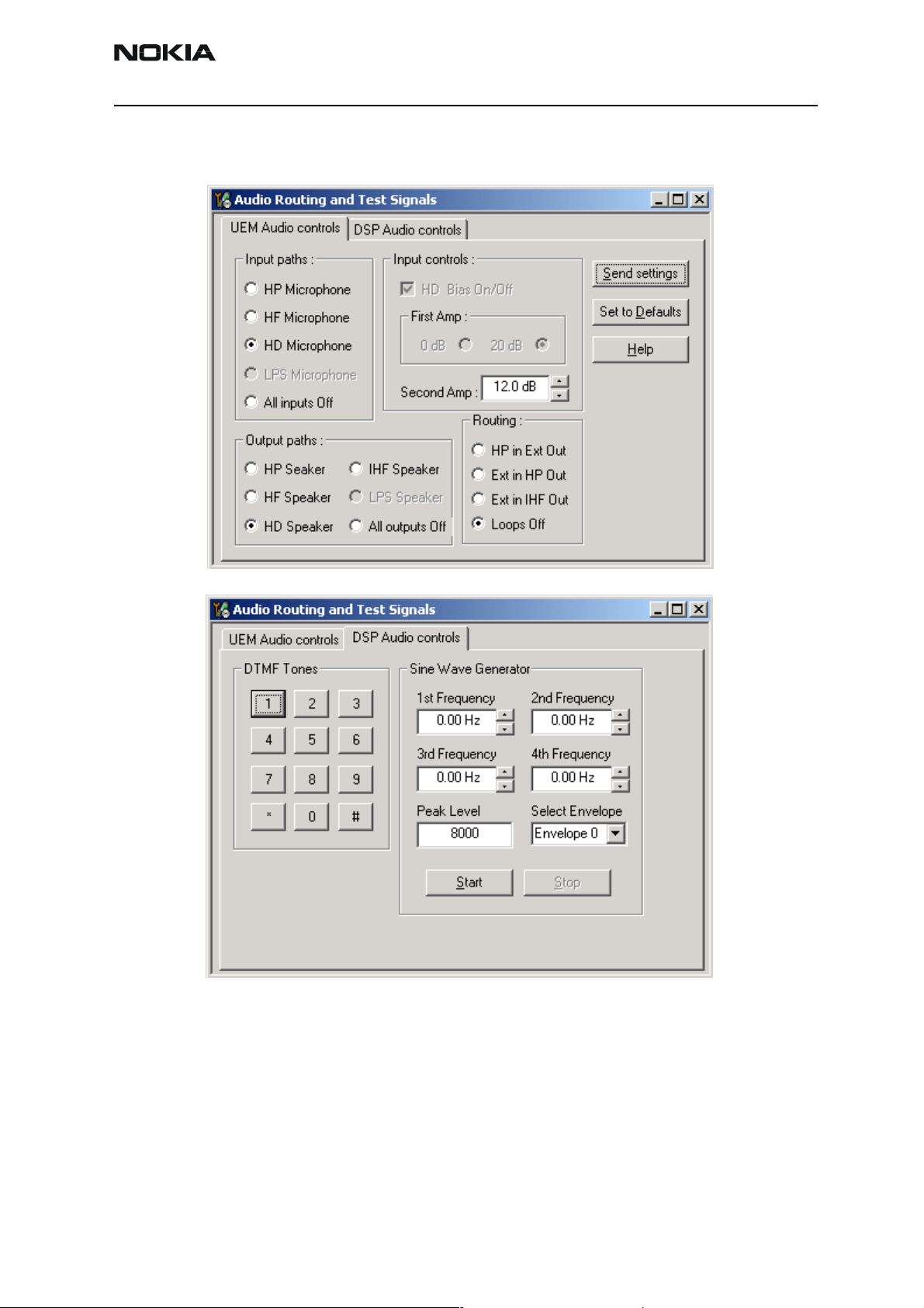
Audio troubleshooting
Figure 7: Audio routing window in Phoenix
Issue 2 09/2004 Copyright © 2004 Nokia Corporation Page 6-33
Company Confidential
Page 34

NEM-4 Company Confidential
6 - Troublehsooting Instructions Nokia Customer Care
Microphone
Page 6-34 Copyright © 2004 Nokia Corporation Issue 2 09/2004
Company Confidential
Page 35

Company Confidential NEM-4
Nokia Customer Care 6 - Troublehsooting Instructions
Earpiece
Check that holes are not coated.
Issue 2 09/2004 Copyright © 2004 Nokia Corporation Page 6-35
Company Confidential
Page 36
NEM-4 Company Confidential
6 - Troublehsooting Instructions Nokia Customer Care
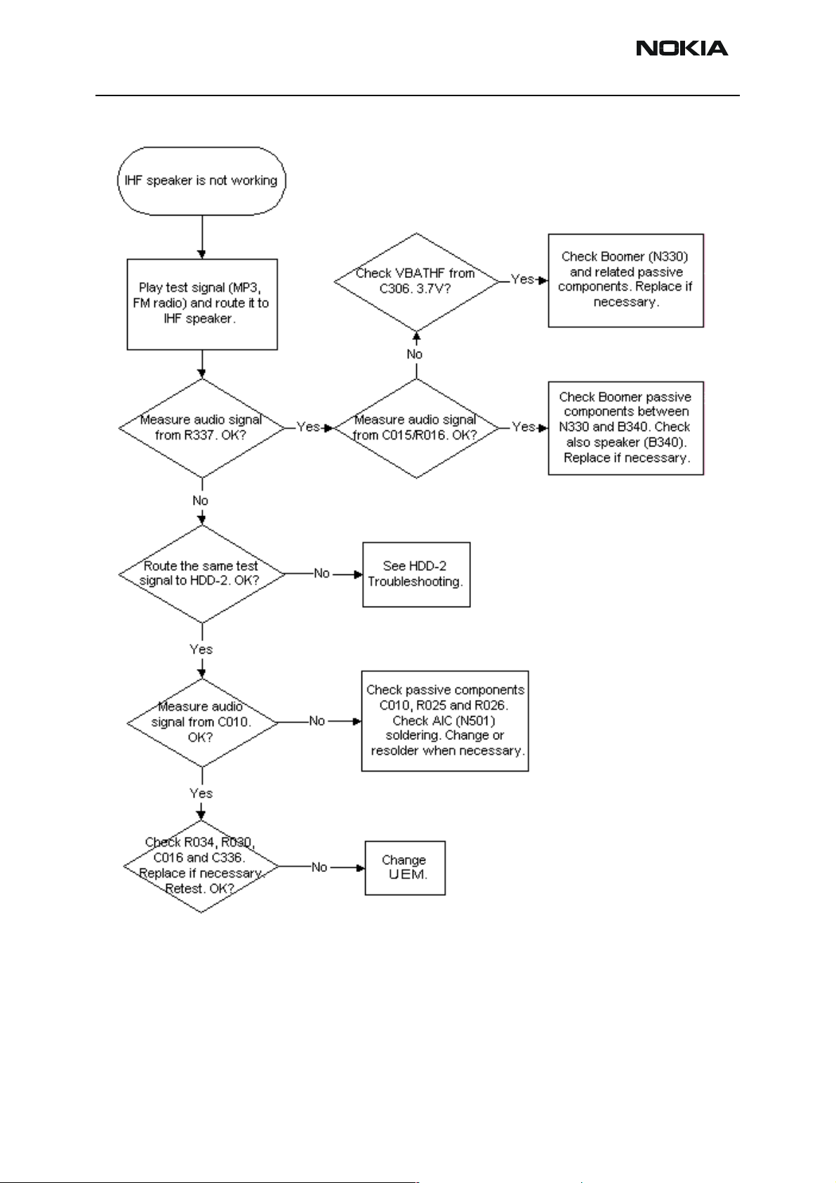
IHF
Page 6-36 Copyright © 2004 Nokia Corporation Issue 2 09/2004
Company Confidential
Page 37

Company Confidential NEM-4
Nokia Customer Care 6 - Troublehsooting Instructions
Headset troubleshooting
Issue 2 09/2004 Copyright © 2004 Nokia Corporation Page 6-37
Company Confidential
Page 38
NEM-4 Company Confidential
6 - Troublehsooting Instructions Nokia Customer Care
Page 6-38 Copyright © 2004 Nokia Corporation Issue 2 09/2004
Company Confidential
Page 39
Company Confidential NEM-4
Nokia Customer Care 6 - Troublehsooting Instructions
Memory troubleshooting
Most memory related errors are found through flashing the device, flashing the device is
therefore recommended before any of the steps described in this chapter. Check flashing
Troubleshooting section first.
There are however a few memory related errors that cannot be found through flashing.
• SDRAM(D312) partially damaged. This can mean that the SDRAM component
itself is partially damaged and all the memory locations cannot be successfully
read or there is a soldering problem somewhere either under UPP or SDRAM.
There is a BB self test for testing SDRAM component quite thoroughly, but the
problem is that if SDRAM doesn't function properly one may not be able to run
those tests as SDRAM is used during the device boot and selftest cannot be run if
the device hasn't booted.
• DEVICE may inform about being "out of memory " more often than it should
• flash1 (D310) or flash 2 (D313) is partially/totally damaged. During flashing the
manufacturer, device and revision id's are read, but flashing is done based on id's
of the flash0 (D311). This means that one cannot see any error messages displayed on Phoenix window during flashing if flash1 or flash 2 is failing. Id's are
however displayed on the Phoenix window and successful read of flash1 id's can
be checked from there.
Issue 2 09/2004 Copyright © 2004 Nokia Corporation Page 6-39
Company Confidential
Page 40
NEM-4 Company Confidential
6 - Troublehsooting Instructions Nokia Customer Care
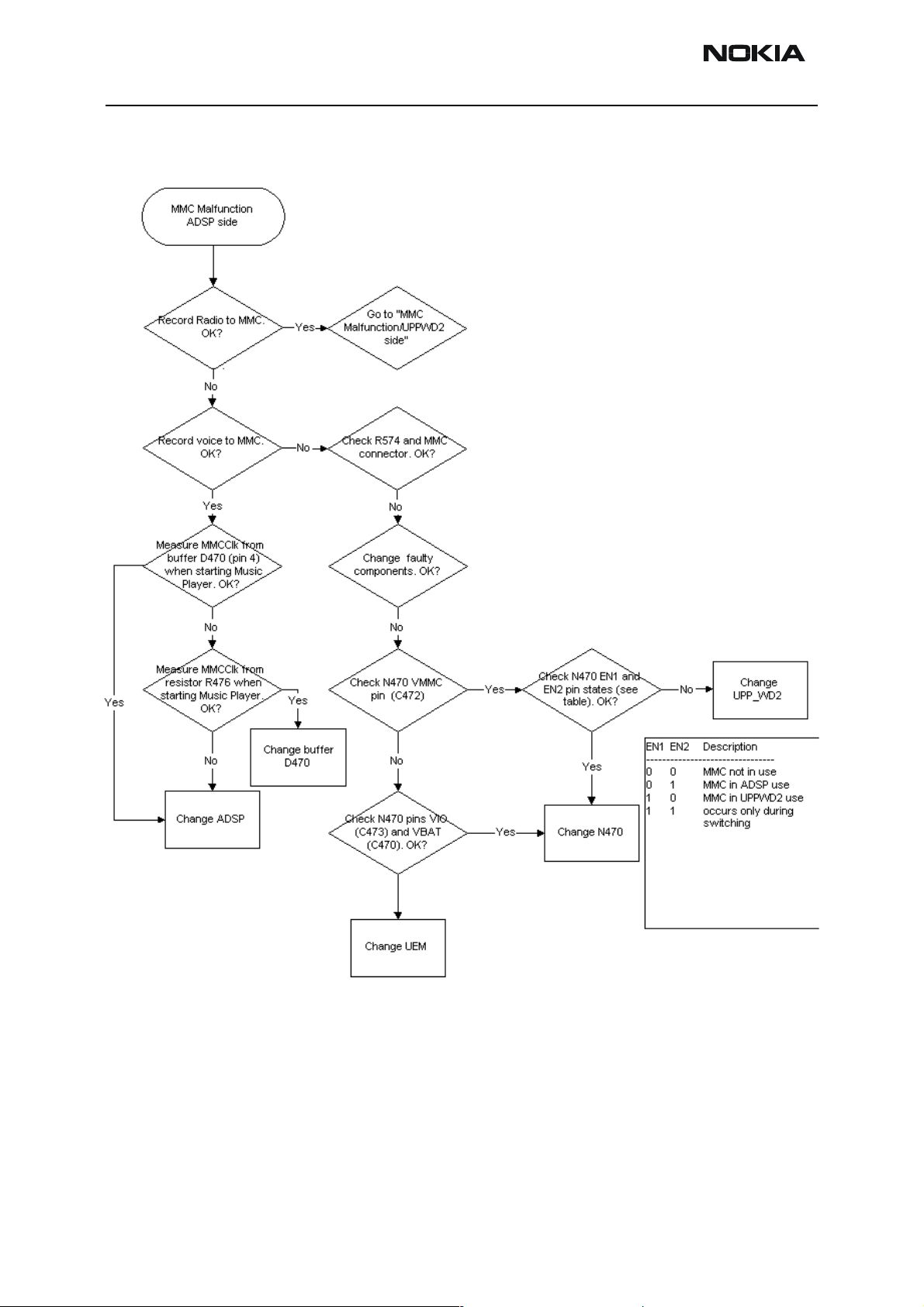
MMC troubleshooting
Page 6-40 Copyright © 2004 Nokia Corporation Issue 2 09/2004
Company Confidential
Page 41

Company Confidential NEM-4
Nokia Customer Care 6 - Troublehsooting Instructions
Issue 2 09/2004 Copyright © 2004 Nokia Corporation Page 6-41
Company Confidential
Page 42
NEM-4 Company Confidential
6 - Troublehsooting Instructions Nokia Customer Care
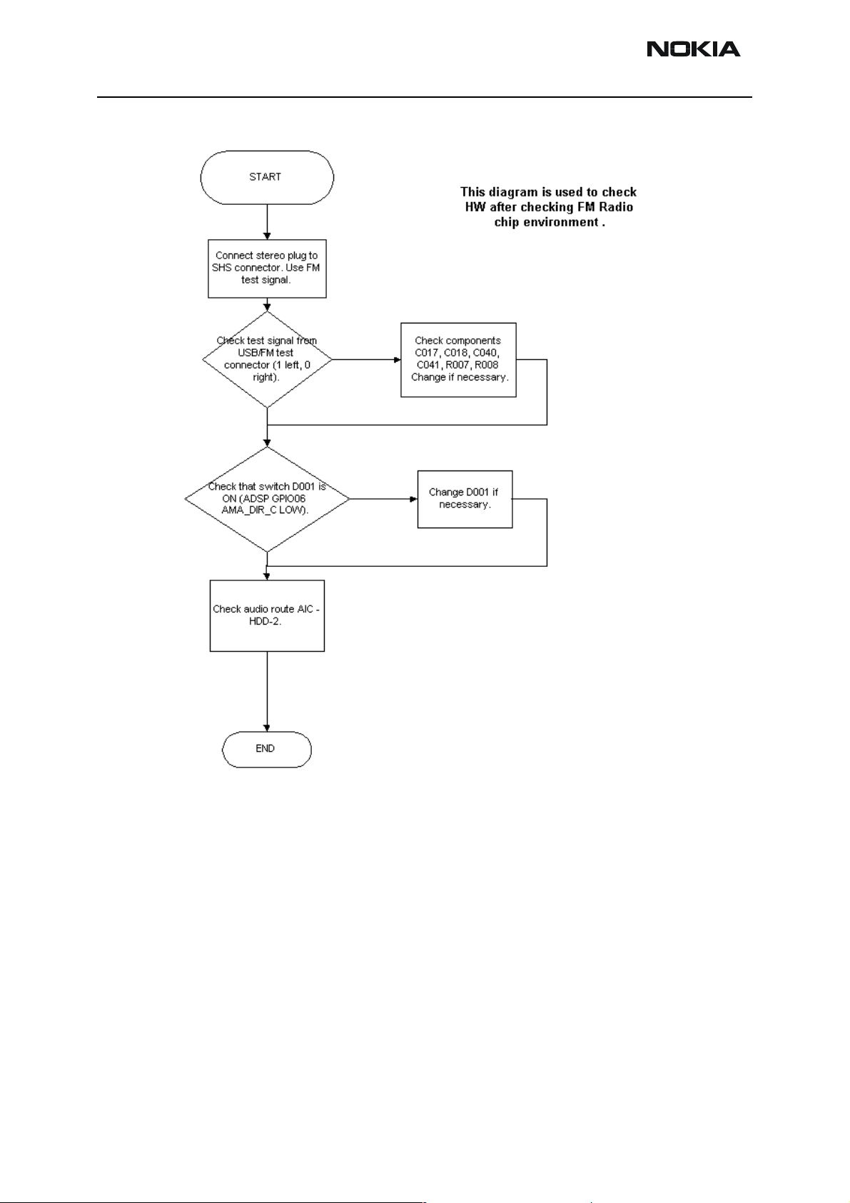
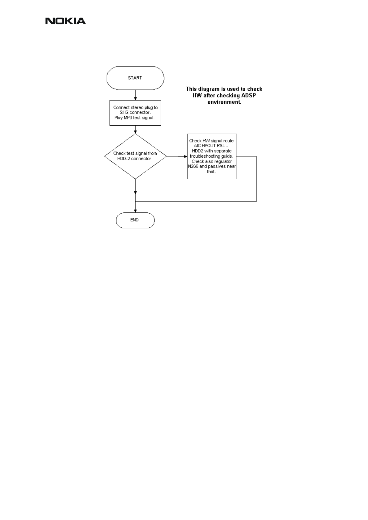
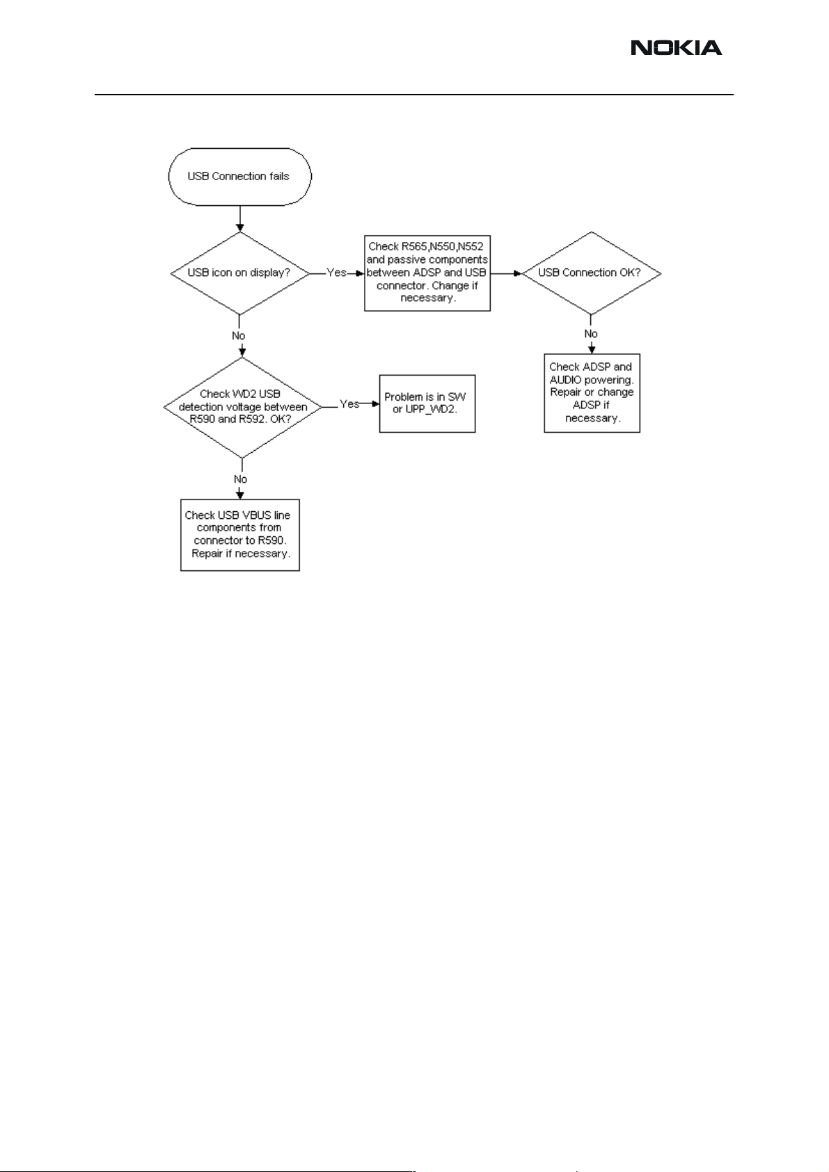
USB troubleshooting
Page 6-42 Copyright © 2004 Nokia Corporation Issue 2 09/2004
Company Confidential
Page 43
Company Confidential NEM-4
Nokia Customer Care 6 - Troublehsooting Instructions
VIBRA
There may be three kind of problems concerning vibra; it doesn't rotate at all, it's noisy or
it's continuously on. The noisiness is usually caused by the surrounding mechanics when
the rotating mass has contact to it.
Vibra
Malfunction
Change UEM
No
Vibra doesn’t rotate
Yes
Is the Vibra jammed
or its contact pads
No
Measure that C134 is
pulsed down to zero
while Vibra is switched
Yes
worn
on.
Vibra is continuously
on
Vibra is noisy
Check the
surrounding
mechanics of
the Vibra
Is it Vibra
component itself
that makes
noise?
No
Yes
Check C134, C135,
V132 and V131
Change the Vibra
and retest.
Vibra works
Issue 2 09/2004 Copyright © 2004 Nokia Corporation Page 6-43
Company Confidential
Page 44

NEM-4 Company Confidential
6 - Troublehsooting Instructions Nokia Customer Care
ZOCUS
Read phone current
Read phone current
consumption
consumption
in Phoenix
in Phoenix
Y
OK?
OK?
N
N
Check N301
Check N301
and other
and other
components
components
Y
SW Error Reflash
SW Error Reflash
N
N
Replace damaged
Replace damaged
components and retest
components and retest
component
component
UI Troubleshooting
UI troubleshooting cases
This document describes how the trouble shooting should be done if there is something
wrong with the UI function. If the problem is due to the display or keymat PWB the
whole UI module should be replaced. However, the earpiece maybe replaced. (see Audio
Troubleshooting)
Replace
Replace
Page 6-44 Copyright © 2004 Nokia Corporation Issue 2 09/2004
Company Confidential
Page 45

Company Confidential NEM-4
Nokia Customer Care 6 - Troublehsooting Instructions
Keymat backlight
If the keymat backlight is non-functional and the backlight driver voltage is generated
correctly, then there is either a problem with the connector or the UI module.
Note: that it is possible for an LED to be non-functional and for all other LEDs to still be
working.
Issue 2 09/2004 Copyright © 2004 Nokia Corporation Page 6-45
Company Confidential
Page 46
NEM-4 Company Confidential
6 - Troublehsooting Instructions Nokia Customer Care
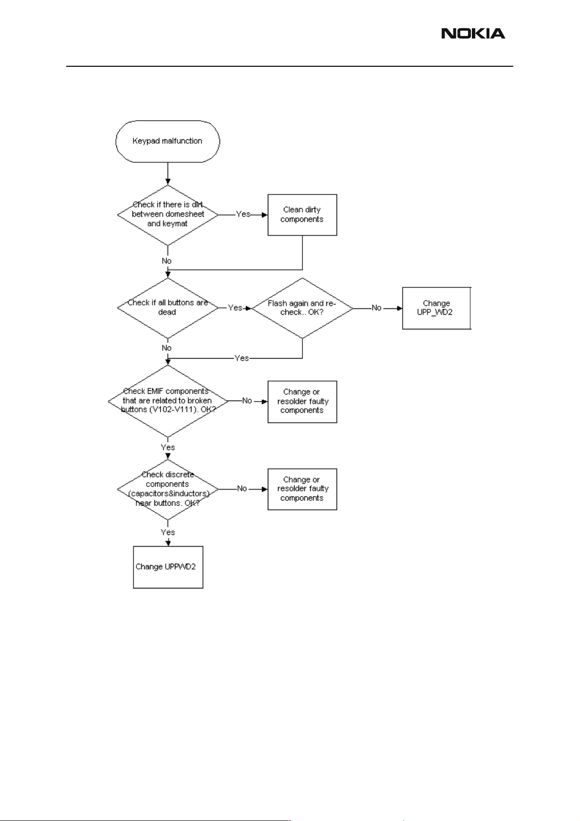
Keyboard
If keyboard doesn’t work, follow the troubleshooting flow chart below:
Page 6-46 Copyright © 2004 Nokia Corporation Issue 2 09/2004
Company Confidential
Page 47
Company Confidential NEM-4
Nokia Customer Care 6 - Troublehsooting Instructions
Display blank
Display blank
Display blank
Y
Replace
Replace
Display
Display
N
N
Check test points
Check test points
J113, J114,
J113, J114,
J185-J191
J185-J191
Y
Display ok
Display ok
OK?
OK?
N
N
Change
Change
UPPWD2
UPPWD2
Y
Y
Change V101
Change V101
Z130
Z130
Issue 2 09/2004 Copyright © 2004 Nokia Corporation Page 6-47
Company Confidential
Page 48

NEM-4 Company Confidential
6 - Troublehsooting Instructions Nokia Customer Care
Backlight does not turn on
Page 6-48 Copyright © 2004 Nokia Corporation Issue 2 09/2004
Company Confidential
Page 49
Company Confidential NEM-4
Nokia Customer Care 6 - Troublehsooting Instructions
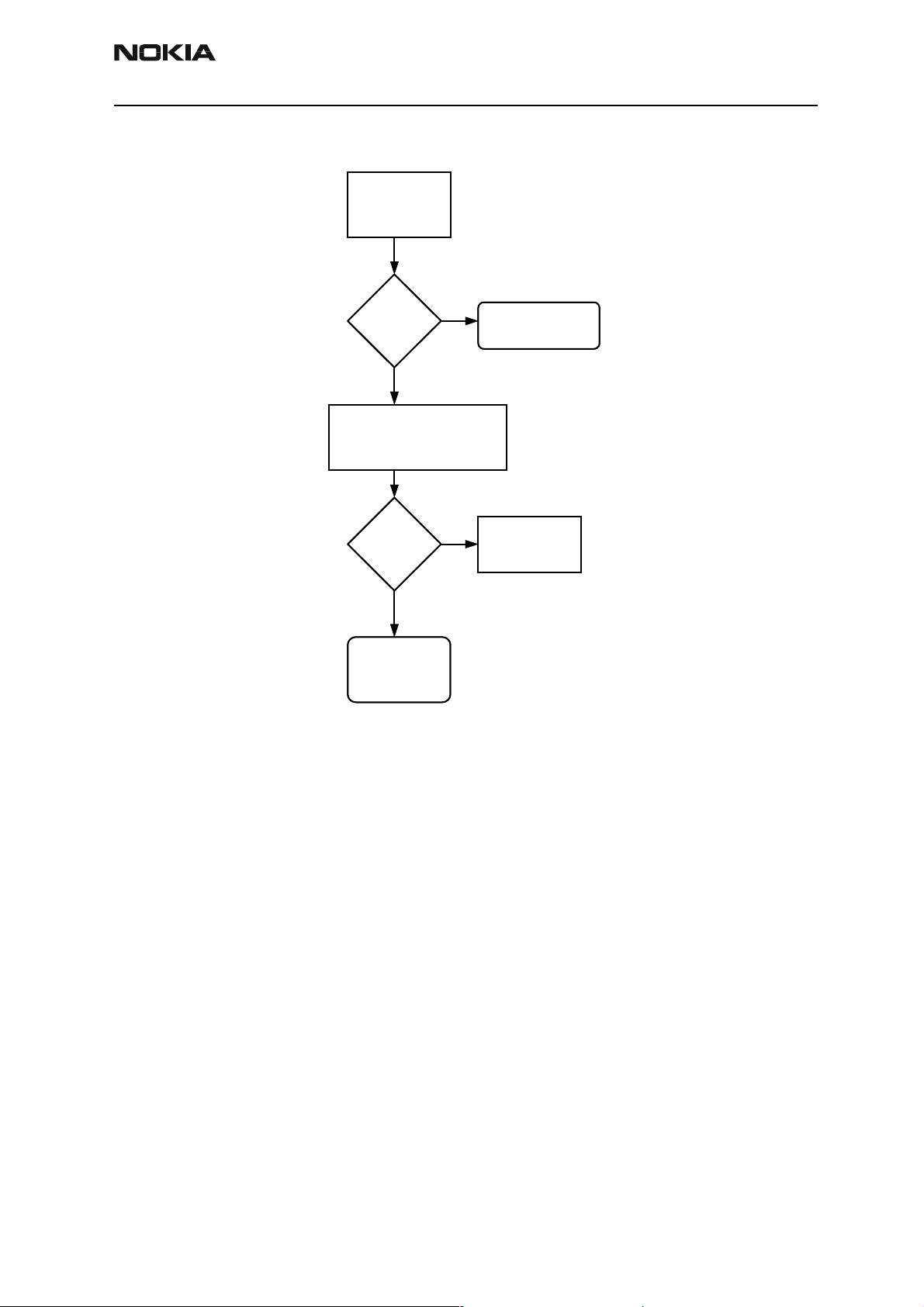
FM Radio Troubleshooting
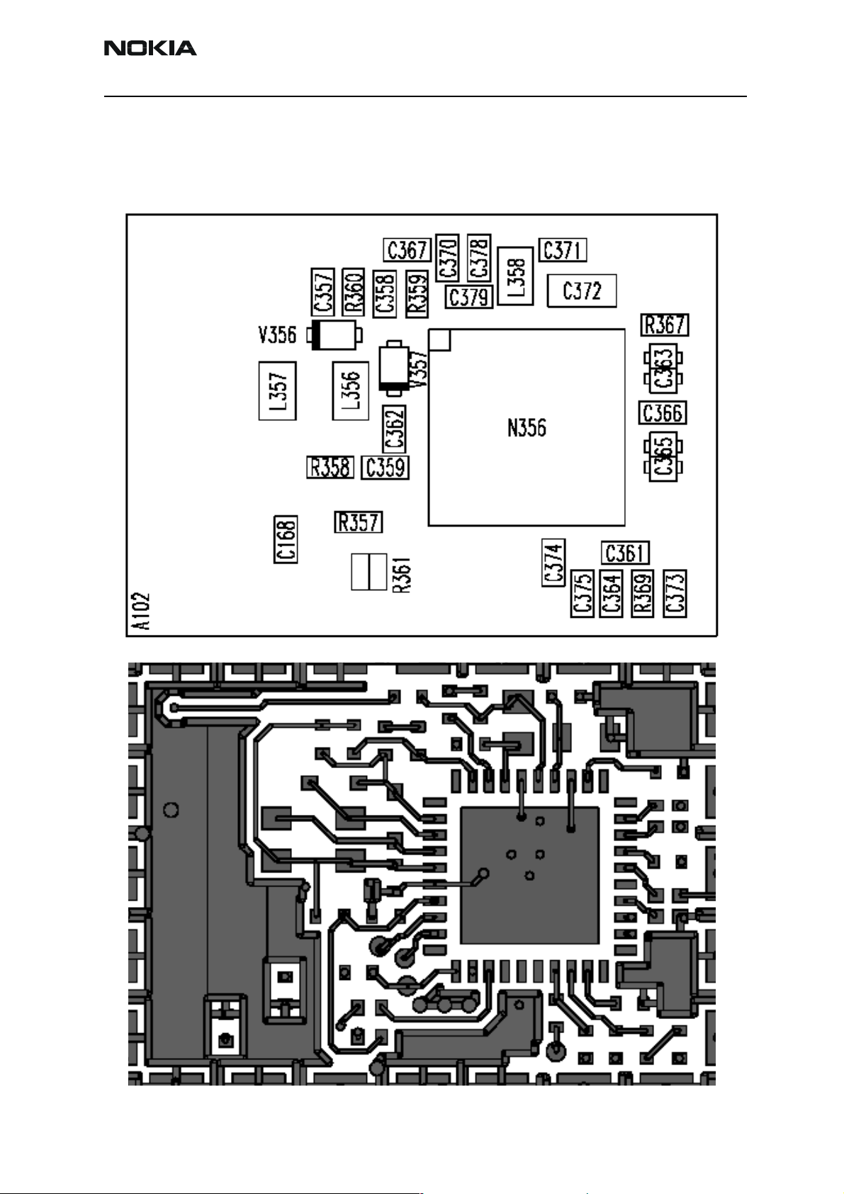
FM radio component layout
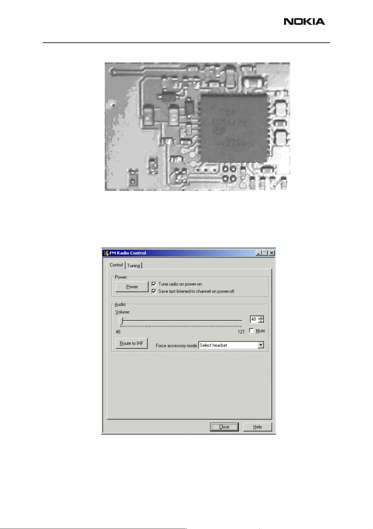
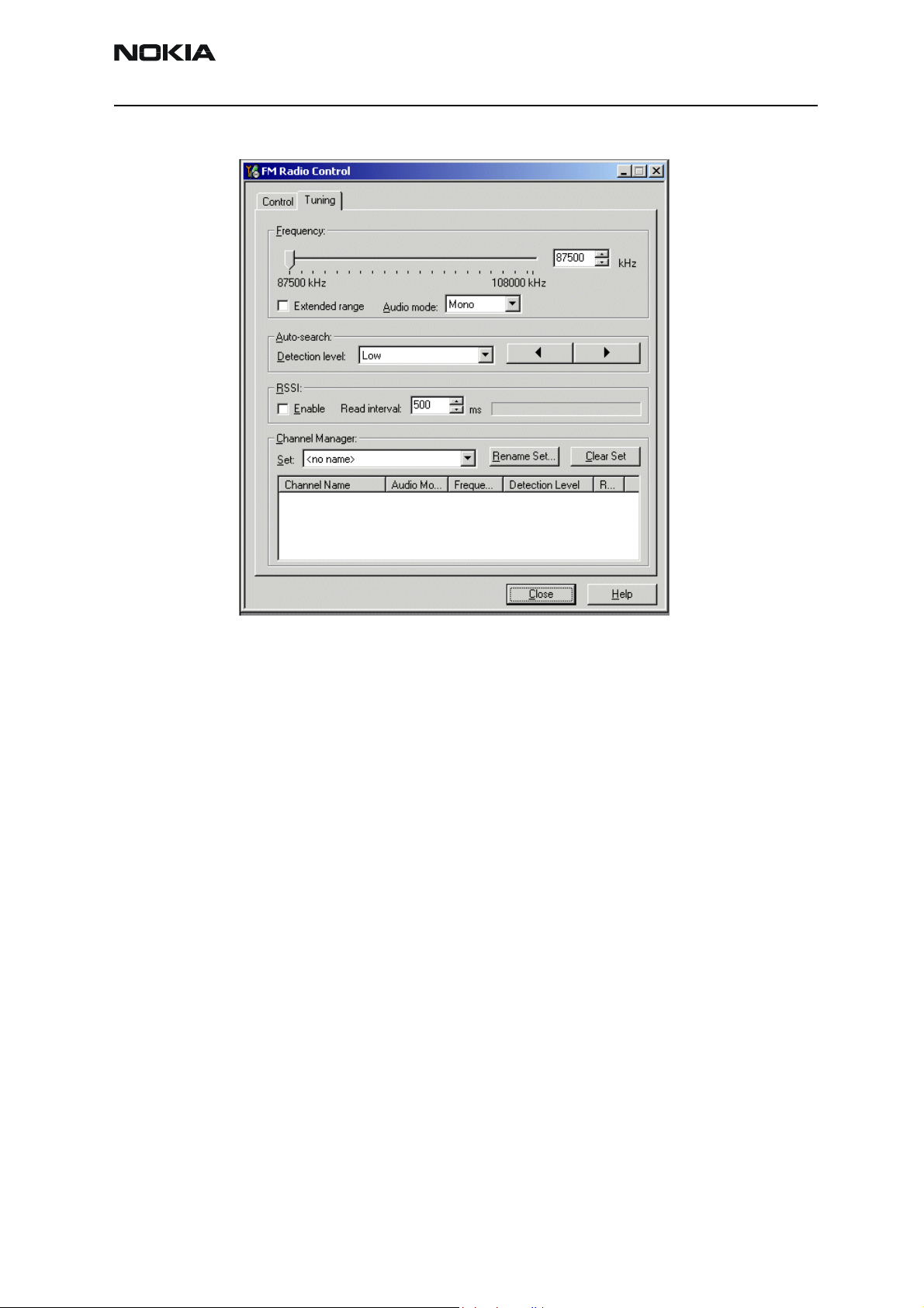
Figure 8: Component placement
Figure 9: Trace layout.
Issue 2 09/2004 Copyright © 2004 Nokia Corporation Page 6-49
Company Confidential
Page 50
NEM-4 Company Confidential
6 - Troublehsooting Instructions Nokia Customer Care
Figure 10: FM radio block layout.
Components C001 and C002 are not shown in the picture. Those components are placed
near audio connector X002.
Figure 11: FM Radio control window.
Page 6-50 Copyright © 2004 Nokia Corporation Issue 2 09/2004
Company Confidential
Page 51
Company Confidential NEM-4
Nokia Customer Care 6 - Troublehsooting Instructions
FM radio troubleshooting diagram
Notes to "FM Radio Troubleshooting diagram"
Use 1MHz 1X probe when measuring Audio and clock signals with oscilloscope.
Use active RF probe when measuring frequencies with spectrum analyzer.
Note 1. RF test signal parameters:
• Amplitude, A, –67.0 dBm
• Carrier frequency, f
•Deviation,
• Modulating frequency fm, 1,000 kHz (RF generator internal)
• FM stereo, mode R=L, pilot state ON
∆
f, 75 kHz
, 98,000 MHz
c
Issue 2 09/2004 Copyright © 2004 Nokia Corporation Page 6-51
Company Confidential
Page 52
NEM-4 Company Confidential
C521, C522, R50
N
C
C
C
N
N
C
6 - Troublehsooting Instructions Nokia Customer Care
Figure 12: FM radio troubleshooting diagram
Set phone into local mode.
Start FM radio.
Does
the radio
start ?
YES
Connect RF test signal (note1)
Set radio channel to 98.0 MHz
Set radio volume to max.
Measure
Audio signal
C017 and
from C162 and
C018
C163.
Is it 1kHz
0.5–0.8Vp–p?
NO
Check
516, C519
C107, C108,
C501, C502, C001
C109, C117 ,
L105,C367,C378,
C002, L500, L503
C379, L358.
Measure signal
C017, C018
from C162, C163
Is it 1kHz
0.5–0.8
Vp–p?
NO
Check
R503, R504, V500
R359,R360,
V356, V357,
V501 , L501, L502
L356,L357,C357,
C512, C513, C511
C358,C362.
Measure
signal from
J103, J104,
OK ?
NO
Change
500
N356.
Measure signal
from J103 and J104.
Is it
OK ?
Check
NO NO
YES
YES
YES
YES
C374, C375, R375,
R358 and measure
32kHz clock signal
from J359,
retest starting.
Start OK ?
Check
005, C006, R028
R164,
R165, R166,
R029, L002, L003
R167, L103,L104
Measure
signal from J103
and J104.
Is it
0.015–0.3
Vp–p?
5
L511
YES
OK, RETEST IN FLALI
NO
YES
Measure
voltages from
pins 7 and 34,
is it –2.7 V ?
Retest starting.
Start OK now ?
Radio and RF generator
R503, R504, V500, V501
L357, C357, C358, C362,
L501, L502, C512, C513, C511
Set
to 87.5 and 108.0 MHz.
Measure Audio from
017, C018
C162 and C163.
Are both cases
1 kHz 0.5 – 0.8 Vp–p ?
Check
V356, V357, L356,
R359, R360.
T est again with
87.5 and 108.0 MHz.
Measure audio from
C017, C018
C162 and C163.
Both
OK?
NO
Change
500
V356 and 357.
BOTH !
Retest with
87.5 and 108.0 MHz.
Measure audio from
017, C018
C162 and C163.
Both OK ?
NO
NO
NO
Check
N500
N356 solders
(pins 5,6,7,8,9,11,
12,13,17,33,34,35,
36, 37.
Start OK
now ?
YESYES
Baseband digital
YES
YES
Change
500
N356.
Radio start
OK
now?
NO
fault (UPP)
YES
Audio
Amplifier
failure
(N150)
NO
NO
Change
radio module TB4
OK, RETEST IN FLALI
E Nokia Corporation
Page 6-52 Copyright © 2004 Nokia Corporation Issue 2 09/2004
Company Confidential
Page 53
Company Confidential NEM-4
Nokia Customer Care 6 - Troublehsooting Instructions
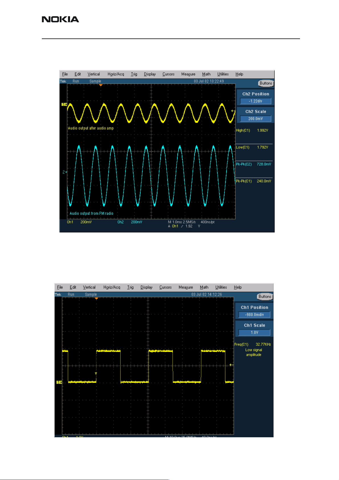
Diagrams of FM radio signals
Figure 13: Oscilloscope screen shot, Audio output
Signal 1: Audio output from PWB test points J103 and J104, with FM test signal, volume
100%.
Signal 2: Audio output from FM radio pins 22 and 23(same as in C017 and C018), with
FM test signal
Figure 14: FM radio clock from L511, 32 kHz frequency clock signal, when radio is on.
Issue 2 09/2004 Copyright © 2004 Nokia Corporation Page 6-53
Company Confidential
Page 54
NEM-4 Company Confidential
6 - Troublehsooting Instructions Nokia Customer Care
Figure 15: FM frequency from FM radio pin 37, the other end of L500, with FM test signal
15:51:49 03 JUL 2002
PEAK
LOG
10
dB/
#AT 0 dBREF -20.0 dBm
MKR 97.9280 MHz
-71.03 dBm
SWEEP
CONT SGL
FREE RUN
VIDEO
LINE
WA SB
CORR
SC FS
CENTER 98.0000 MHz SPAN 300.0 kHz
#RES BW 10 kHz VBW 10 kHz #SWP 1.00 sec
EXTERNAL
SYNC CRD
TV TRIG
Figure 16: VCO frequency from FM radio pins 3 and 4, the other ends of V500 and V501, with FM test signal
10:46:24 03 JUL 2002
PEAK
LOG
10
dB/
WA SB
CORR
SC FS
#AT 10 dBREF .0 dBm
MKR
196.440 MHz
-9.40 dB
MEAS UNCAL
SWEEP
CONT SGL
FREE RUN
VIDEO
LINE
EXTERNAL
SYNC CRD
CENTER 196.450 MHz SPAN 1.000 MHz
#RES BW 10 kHz #VBW 10 kHz #SWP 20.0 msec
TV TRIG
Page 6-54 Copyright © 2004 Nokia Corporation Issue 2 09/2004
Company Confidential
Page 55

Company Confidential NEM-4
Nokia Customer Care 6 - Troublehsooting Instructions
RF Troubleshooting
Abbreviations in fault finding charts
BB Base band
DCS/PCN GSM1800
PCS GSM1900
EGSM Extended GSM900
ESD Electro Static Discharge
GPRS General Packed Radio Service
HSCSD High Speed Circuit Switched Data
LO Local Oscillator
PA Power Amplifier
PWB Printed Wired Board
PLL Phase Locked Loop
RF Radio Frequency
RX Receiver
SA Spectrum analyzer
TX Transmitter
UHF Ultra High Frequency
VCO Voltage controlled oscillator
VHF Very High Frequency
Issue 2 09/2004 Copyright © 2004 Nokia Corporation Page 6-55
Company Confidential
Page 56

NEM-4 Company Confidential
6 - Troublehsooting Instructions Nokia Customer Care
Introduction
Two types of measurements have to be done for repair of the phone boards:
• RF measurements shall be done using a Spectrum Analyzer together with a highfrequency probe. (Note, that signal will be significantly attenuated). Correct
attenuation can be checked by using a “good” phone board, for example.
• LF (Low frequency) and DC measurements shall be done with a an oscilloscope
together with an 10:1 probe.
Always make sure that the measurement set-up is calibrated when measuring RF parameters at the RF connector. Remember to include the correct losses in the module repair
jig and the connecting cable when realigning the phone.
Most RF semiconductors are static discharge sensitive. ESD protection must be taken
into account during repair (ground straps and ESD soldering irons).
Mjoelner RF ASIC is moisture sensitive. Therefore, Mjoelner RF ASIC must be pre-baked
prior to soldering.
Rx calibration done via Phoenix software is temperature sensitive because of calibration of 26 MHz reference oscillator (VCXO). According to Mjoelner specification
ambient temperature has to be in a range from 22°C to 36°C.
Apart from key-components described in this document there are a lot of discrete components (resistors, inductors and capacitors) for which Troubleshooting is done by checking if soldering of the component is done properly and checking if the component is
missing from PWB. Capacitors can be checked for short-circuiting and resistors for value
by means of an ohm-meter, but be aware in-circuit measurements should be evaluated
carefully.
In the following both, the name EGSM and EGSM900 will be used for the low band. DCS
or PCN and GSM1800 will be used for the mid band. PCS and GSM1900 will be used for
the high band.
Page 6-56 Copyright © 2004 Nokia Corporation Issue 2 09/2004
Company Confidential
Page 57
Company Confidential NEM-4
Nokia Customer Care 6 - Troublehsooting Instructions
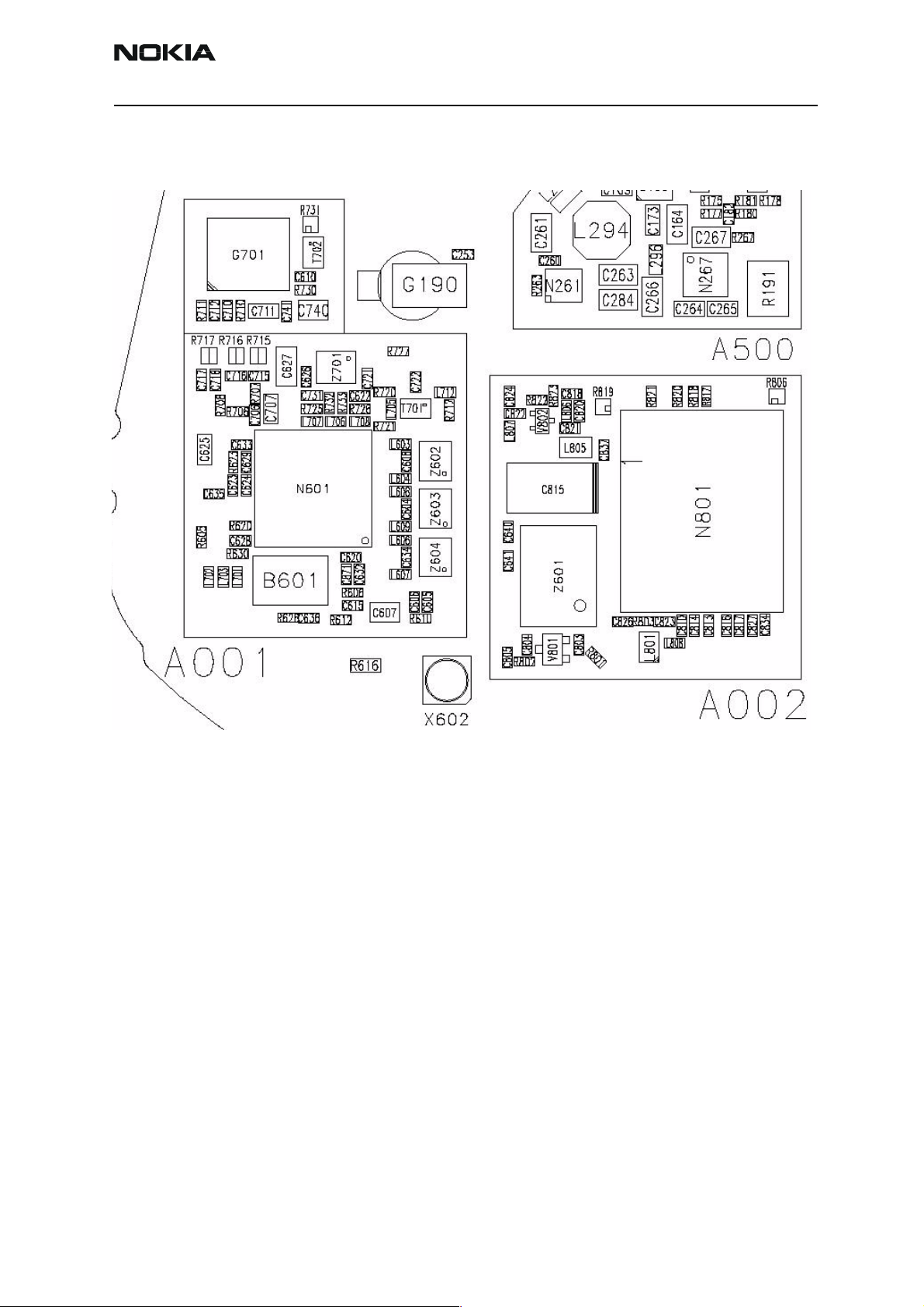
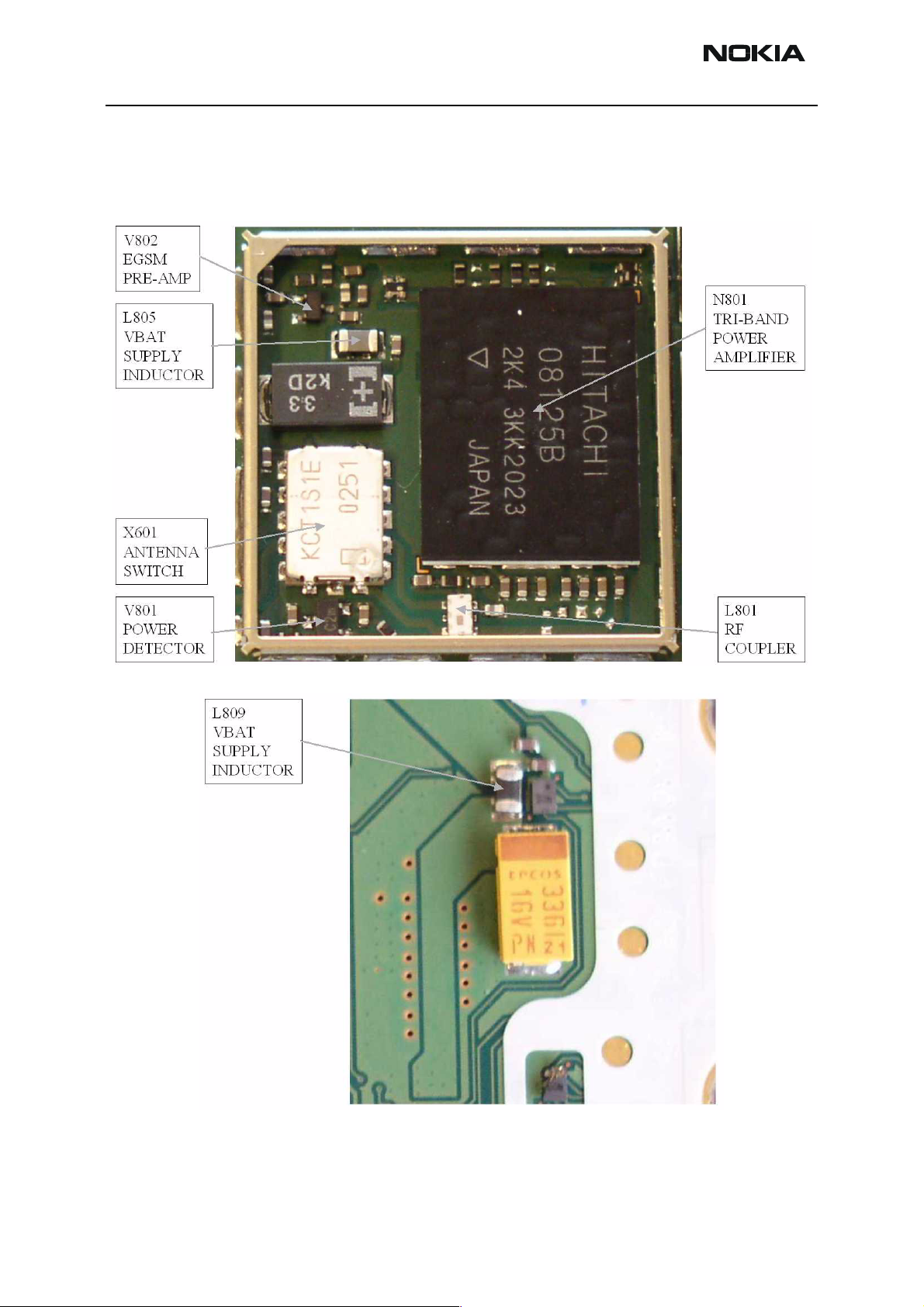
RF key component placement
Figure 17: RF key component placement
Issue 2 09/2004 Copyright © 2004 Nokia Corporation Page 6-57
Company Confidential
Page 58
NEM-4 Company Confidential
6 - Troublehsooting Instructions Nokia Customer Care
Reference
number
N601 Mjoelner RF ASIC X602 RF Connector
B601 26 MHz Xtal L801 Directional Coupler
Z602 GSM1800 RX SAW V801 Detector Diode
Z603 GSM1900 RX SAW Z601 Antenna switch
Z604 EGSM RX SAW filter N801 Power Amplifier
Z701 EGSM TX SAW filter
T701 GSM1800/GSM1900 TX Balun
V802 EGSM Pre-amplifier
G701 3.7 GHz VCO
T702 VCO Balun
Name
Reference
number
Name
RF measurement points
RF supply points
Figure 18: RF Supply points inside Mjoelner can
RF power supplies are generated in the UEM and can be measured either in the Mjoelner
can or in the baseband can. Arrows mark the measurement points inside the pictures.
Page 6-58 Copyright © 2004 Nokia Corporation Issue 2 09/2004
Company Confidential
Page 59

Company Confidential NEM-4
Nokia Customer Care 6 - Troublehsooting Instructions
Measurement points in the receiver
Measurement points are indicated on the picture below.
Figure 19: Rx I and Q measurement points
Figure 20: Rx measurement points at Rx SAW filters and Mjoelner RF ASIC
Issue 2 09/2004 Copyright © 2004 Nokia Corporation Page 6-59
Company Confidential
Page 60
NEM-4 Company Confidential
6 - Troublehsooting Instructions Nokia Customer Care
Measurement points in the transmitter
Measurement points are shown in the picture below,
Figure 21: Tx measurement points inside PA can (bottom side of PWB)
Figure 22: Tx measurement points on the top side of PWB
Page 6-60 Copyright © 2004 Nokia Corporation Issue 2 09/2004
Company Confidential
Page 61

Company Confidential NEM-4
Nokia Customer Care 6 - Troublehsooting Instructions
Figure 23: Tx measurement points inside Mjoelner can
Issue 2 09/2004 Copyright © 2004 Nokia Corporation Page 6-61
Company Confidential
Page 62

NEM-4 Company Confidential
X
6 - Troublehsooting Instructions Nokia Customer Care
RF in General
The RF part is a triple-band direct conversion transceiver. Using direct conversion no
intermediate frequencies are used for up- or down- conversion.
The VCO is set to either twice or four times (depending on the band used) the wanted RX
or TX frequency. The VCO frequency is divided by either 2 or 4 and fed to the mixers
(down-conversion) or modulators (up-conversion). Up- or down- conversion is done in
one step, directly between RF frequency and DC. All up and down-conversion takes place
in the RF ASIC named Mjoelner (N601).
Mjoelner RF ASIC also contains PLL and LNAs for all used bands. A DC control section is
included in to power and/or control EGSM TX buffer, detector and antenna switch. The
Mjoelner RF ASIC is controlled via a serial bus.
Mjoelner RF ASIC contains an integrated VCXO which uses an external 26 MHz Xtal. No
analogue AFC signal is needed. AFC is done via the serial interface of Mjoelner.
The interface between Mjoelner RF ASIC, UPP and Bluetooth uses a 26 MHz reference
clock. An external 26 MHz reference clock buffer is used to drive Bluetooth module.
The RF supports HSCSD (High Speed Circuit Switched Data) and GPRS (General Packed
Radio Service), meaning multi-slot operation, this will not require special equipment or
procedures in repair situations.
Figure 24: RF frequency plan
Mjoelner
EGSM: 925-960 MHz
DCS: 18 05 - 1880 MHz
PCS: 1930-1990 MHz
f/4
f/4
f
f
f/2
f
34203980
MHz
f
f/2
I-signal
Q-signal
RX
PLL
26 MHz
DCS: 17 10 - 1785 MHz
PCS: 1850-1910 MHz
EGSM: 880-915 MHz
1/1
1/2
XTal
LPRFCLK
RFCLK
I-signal
Q-signal
T
Page 6-62 Copyright © 2004 Nokia Corporation Issue 2 09/2004
Company Confidential
Page 63

Company Confidential NEM-4
Nokia Customer Care 6 - Troublehsooting Instructions
VR5
VR1A
5V
VPLL
Vcp
PLL
filter
filter
Synth
supply
supply
CPOUT
VDDCP
VDDPLL
VDDLO
VDDPRE
Pump
Charge
VRX
VR4
RXIP
RXIM
BIQUAD
RXQP
RXQM
DCN2
LPF2
AGC
DCN2
LPF2
BIQUAD
AGC
ϕ
Rx
filter
supply
D
V
D
R
X
B
B
DCN1
LPF1
BBAMP
DCN1
ADIV
NDIV
LPF1
BBAMP
64/65
Mjoelner
VR3
filter
VCXO
supply
REFOUT
LPR
loop
filter
VDDXO
REFOUT
VDDBBB
Lock
1/2
Detect
Buf/
AGC
RDIV
LOCNT
REFCNT
VR7
VR2
VIO
GENIO6
VIO
filter
VCO
supply
CLK
buffer
26MHz
INPLO
XTALP
INMLO
XTALM
Buffer
R2H/R2
VCXO Bias
VBB (1.8V)
RESET_X
Ref clk set
RFBUSX
RFBUSDA
RFBUSCLK
3
VDDDL
VDDDIG
RESETX
Control
AFC/CAL
VDDTX
VDDRXBB
RF_EN
RF_CLK
RF_DATA
RESETX
SELADDR
shift
I/O level
3
VCOSENSE
Digital Control
Sensor
BIST / Temp.
Main Bias Circuit
Resistor Ext/R2H/R2
Rpa
SENSE
PA vendor
indication
2,7k
RBEXT
VBEXT
Ref.
VREF1
filter
RFCONV_0(9)
VDDRXBB
1/4
222
2
4
D
D
V
R
X
F
VR6
Pre-gain
LNA
Bias
LNA
INPL
INML
RX900
SAW
RX
EGSM
Pre-gain
LNA
INPH
INMH
INPM
RX1900
SAW
TX
RX
SAW
TX
PCN
PCS
Ant Switch
1/2
VDDDIG
LNA
INMM
RX1800
VANTL / VANTM / VANTH
3
RX
1/4
1/2
VDDRXB
B
RF
Controls
VB_DET
RF
VTXLOH
VTXLOL
2
2
2
2
Controls
VTXBH
Open collector
VTXBL
OUTHP
OUTHM
Balun
PCN/PCS
PA
Dir. Coupler
Open collector
DET
PLFB1
OUTLP
OUTLM
SAW
VTX
PW-
Buffer
EGSM
PWC
loop
DET
PLFB2
2
2
VDDTX
filter
Supply
TXC
TXP
2
VPCH/VPCL
filter
PA_IDENT
TXIP/TXIM
TXQP/TXQM
VTX
VR2
TXC
TXP
VBATTRF
Figure 25: RF Block diagram
Issue 2 09/2004 Copyright © 2004 Nokia Corporation Page 6-63
Company Confidential
Page 64
NEM-4 Company Confidential
(
(
)
6 - Troublehsooting Instructions Nokia Customer Care
RF Power Supply Configuration
All power supplies for the RF Unit are generated in the UEM IC (D190). All RF supplies
can be checked either in Mjoelner can or in BB can.
The power supply configuration used is shown in the block diagram below. Values of
voltages are given as nominal outputs of UEM. Currents are typical values.
Figure 26: RF Power distribution diagram
UEM
VR1A
4.75V
4.7V)
VR2
(2.78V)
(2.78V)
(2.78V)
(2.78V)
(2.78V)
VREF01
(1.35V)
VR3
VR4
VR5
VR7
VIO
(1.8V)
VBAT
Charge Pump Supply : Vddcp(0.5mA)
TX Modulators(85mA), Bias :
Mjolner registers: Vdddig(10uA)
Mjoelner mixers: OUTXX (66mA)
VCXO Supply : Vddxo(2.7mA)
Vddrxf(7mA), Vddrxbb(30mA)
PLL Supplies : Vddpll(0.5mA), Vddlo
External VCO supply (13mA)
26MHz Buffer, logic : Vddbbb(0.7mA),
Bias Reference : VBEXT(-10uA)
Vddtx(8mA)
BT Buffer (1mA)
RX LNA, RX Mjoner BB :
+ Vddpre(36mA)
Vddl(1uA)
PA, Bluetoot h
Page 6-64 Copyright © 2004 Nokia Corporation Issue 2 09/2004
Company Confidential
Page 65

Company Confidential NEM-4
Nokia Customer Care 6 - Troublehsooting Instructions
Receiver
General instructions for RX troubleshooting
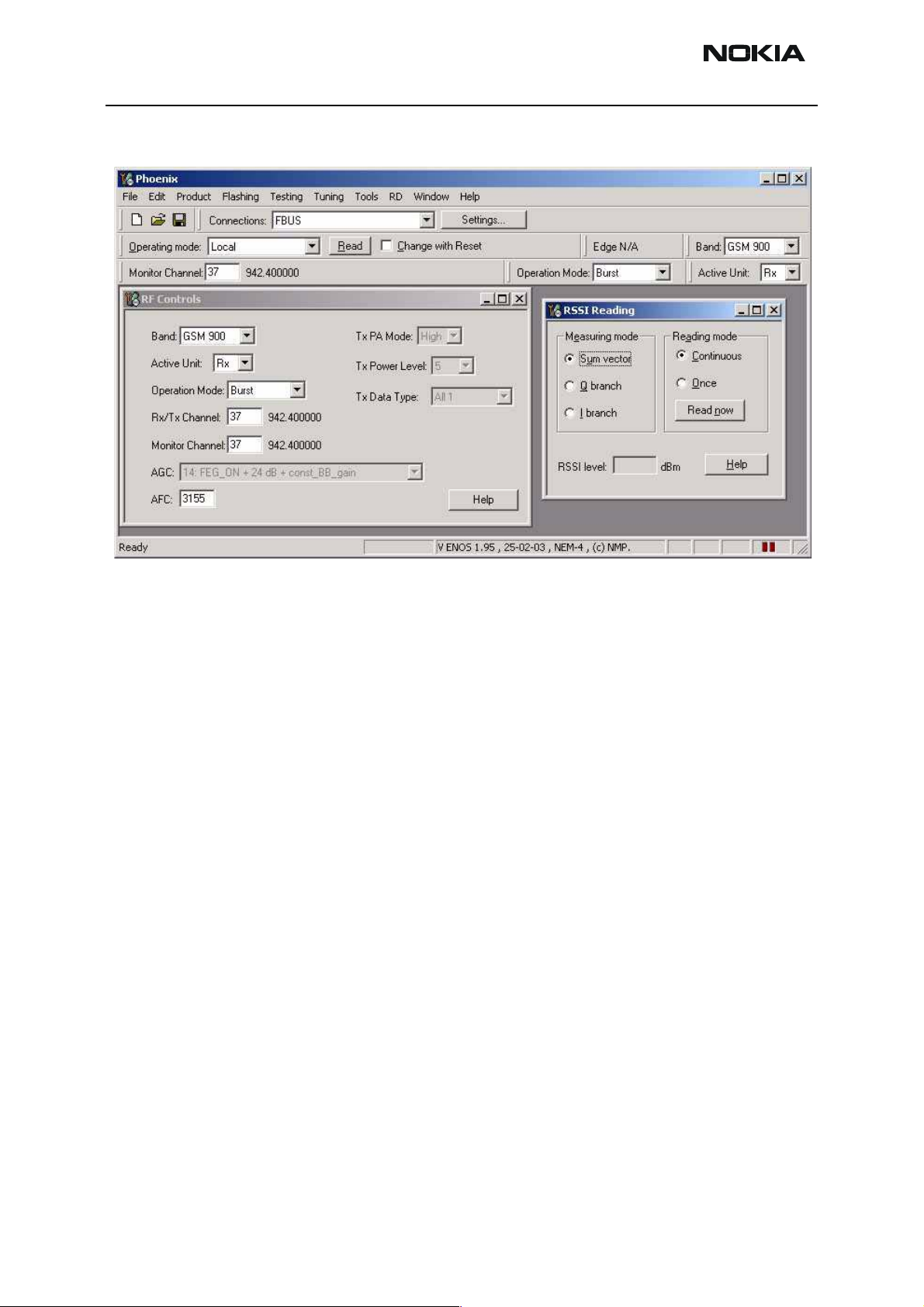
Connect the phone to a PC with DAU-9S cable and dongle and follow the following
instructions:
Measuring RX I/Q signals using RSSI reading
Start Phoenix Service Software
Log in with your user ID.
Select File [Alt-F]
Manage Connections [M]
FBUS Apply
Close window
Open the FBUS connection
Select Scan Product Ctrl-R
Wait until phone information shows in the lower right corner of the screen.
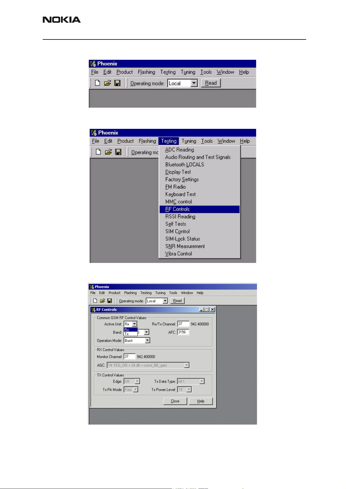
Set operating mode to local mode
Select Testing alt-S
RF Controls R
Wait until the RF Controls window pops up
Select Band GSM 900 or GMS 1800 or GSM 1900
Active unit RX
Operation mode Burst
RX/TX Channel 37 or 700 or 661
Select Testing alt-S
RSSI reading g
The setup should now look like this:
Issue 2 09/2004 Copyright © 2004 Nokia Corporation Page 6-65
Company Confidential
Page 66
NEM-4 Company Confidential
6 - Troublehsooting Instructions Nokia Customer Care
Apply a signal with a frequency of
EGSM : 942.467 MHz (channel 37 + 67.710kHz offset)
GSM1800: 1842.867 MHz (channel 700 + 67.710kHz offset)
GSM1900: 1960.067 MHz (channel 661 + 67.710kHz offset)
and a power level of -80dBm to the RF-connector (remember to compensate for cable
attenuation).
In RSSI reading click on Read now.
Measuring RX performance using SNR measurement
Start Phoenix Service Software
Open the FBUS connection
Select Scan Product Ctrl-R
Wait until phone information is shown in the lower right corner of the screen.
Set operating mode to local mode
Select Testing alt-S
RF Controls R
Page 6-66 Copyright © 2004 Nokia Corporation Issue 2 09/2004
Company Confidential
Page 67
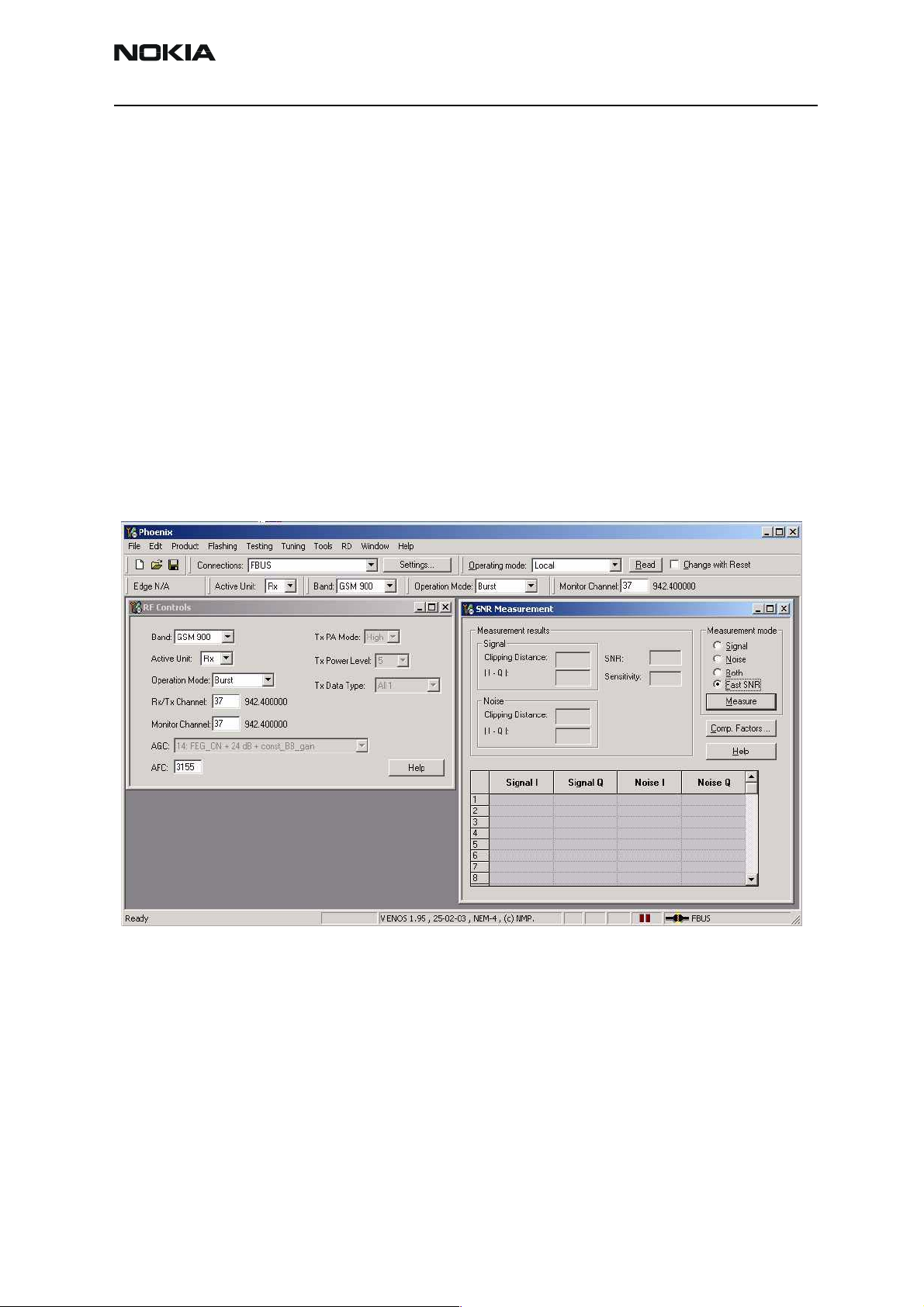
Company Confidential NEM-4
Nokia Customer Care 6 - Troublehsooting Instructions
Wait until the RF Controls window pops up
Select Band GSM 900 or GMS1800 or GSM1900
Active unit RX
Operation mode Burst
RX/TX Channel 37 or 700 or 661
Select Testing alt-S
SNR Measurement N
select Fast SNR Radio Button
The setup should now look like this:
Choose respective band (EGSM900, GSM1800, GSM1900).
Issue 2 09/2004 Copyright © 2004 Nokia Corporation Page 6-67
Company Confidential
Page 68
NEM-4 Company Confidential
6 - Troublehsooting Instructions Nokia Customer Care
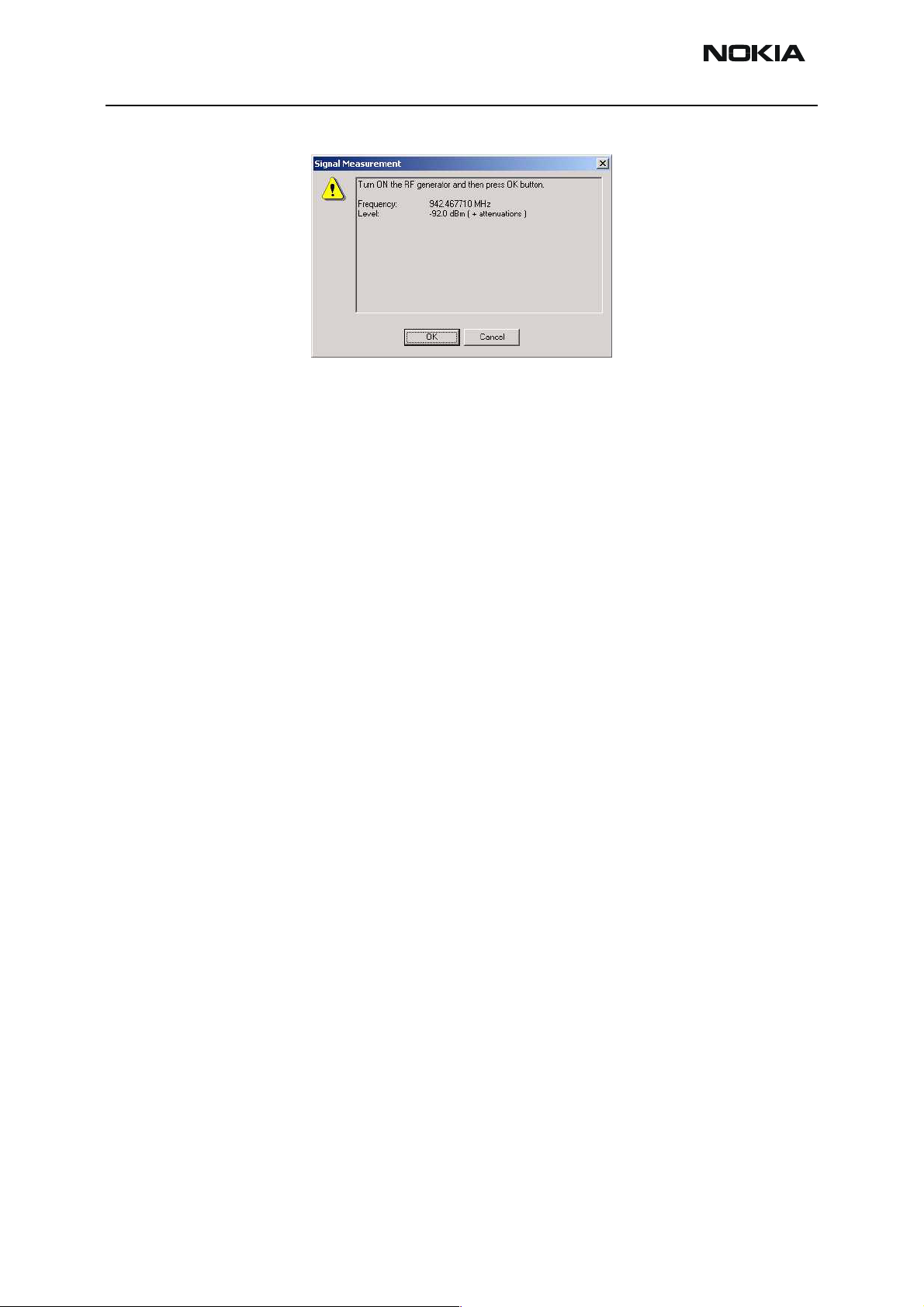
Press measure. A window pops up, e.g. for EGSM900 band:
Connect an external signal generator to the RF connector of the phone and set the generator as told in the window, taking care for external cable losses.
Press ok and the window closes.
Read the SNR result. SNR should be: EGM900 >20dB
GSM1800 >18dB
GSM1900 >18dB
Measuring frontend power levels using spectrum analyzer
Spectrum analyzer (SA) level values depend on the probe type and should be validated using a good sample.
The levels that are given here are measured using a resistive probe (50Ohm semi-rigid
cable).
Start Phoenix Service Software
Open the FBUS connection
Select Scan Product Ctrl-R
Wait until phone information shows in the lower right corner of the screen.
Set operating mode to local mode
Select Testing alt-S
RF Controls S
Wait until the RF Controls window pops up
Select Band GSM 900 or GMS1800 or GSM1900
Active unit RX
Page 6-68 Copyright © 2004 Nokia Corporation Issue 2 09/2004
Company Confidential
Page 69

Company Confidential NEM-4
Nokia Customer Care 6 - Troublehsooting Instructions
Operation mode Continuous
RX/TX Channel 37 or 700 or 661
Please refer to the fault finding chart for proper levels at different test points.
Measuring analogue RX I/Q signal voltages using oscilloscope
Measuring with an oscilloscope on “RXIINN” or “RXQINN” is recommended only if RSSI
reading does not provide enough information. Use testpoints J606-J609. Input level = 80dBm
Start Phoenix Service Software
Select Scan Product Ctrl-R
Wait until phone information shows in the lower right corner of the screen.
Set operating mode to local mode
Select Testing alt-S
RF Controls R
Wait until the RF Controls window pops up
Select Band GSM 900 or GMS1800 or GSM1900
Active unit RX
Operation mode continuous
RX/TX Channel 37 or 700 or 661
AGC 14
Issue 2 09/2004 Copyright © 2004 Nokia Corporation Page 6-69
Company Confidential
Page 70

NEM-4 Company Confidential
6 - Troublehsooting Instructions Nokia Customer Care
Following picture should be seen on a working EGSM receiver:
Signal amplitude 1.25V
DC offset 1,35V
Frequency 67kHz
Receiver fault finding
Set up Phoenix as if doing RSSI measurements.
Ascertain which Rx band is faulty.
Refer to Rx fault finding flow chart.
Set signal generator frequency to 942.47MHz for EGSM, 1842.87MHz for DCS 1800 or
1960.07MHz for PCS 1900.
Set signal generator amplitude to -60dBm.
Note:That checking the RF inputs to SAW filters Z602, Z603 & Z604 will be extremely difficult with
the Mjoelner Can Shield in place. If this is impossible to get to, try checking the test points shown on
the antenna switch Z601.
Page 6-70 Copyright © 2004 Nokia Corporation Issue 2 09/2004
Company Confidential
Page 71

Company Confidential NEM-4
Nokia Customer Care 6 - Troublehsooting Instructions
Select Receive Band
For Testing.
Check Antenna
Switch Cont.
lines. Do they
match the results
in the table?
YES NO
Inspect RF
Connector.
OK?
YES NO
Replace
Antenna
Switch
Replace RF
Connector
NO
Check
L701, L702
L703. OK?
YES
Check Antenna
Switch Test Point.
Signal OK?
YES
Check PI Filter & SAW
Components. OK?
YES
Replace
SAW Filter
NO
Replace all 3
Components
Replace
Inductor
KEY
Test With
Spectrum Analyzer
Check SAW
NO
Output / Mjoelner
Input for band. OK?
NO
Measure Vge at
same point. 0.2V?
Inspect PI filter &
SAW for S/c. S/C?
YES
Rectify S/C
Test With
Oscilloscope
Refer to Synth.
Flow Chart.
YES
NO
NO
Check Mjoelner
Voltage Supplies &
RFBUS lines.
All OK?
Check RSSI using Phoenix.
Does it match Sig. Gen Output level?
NO
Is LO Running?
Probe J606-609 for RX I & Q
NO
Does Waveform
NO
YES
look like example?
YES
YES
Probe J211 &
J212. Is digital
data visible?
YES
NO
YES
Replace
Mjoelner
Inspect /
Check
Refer to BB
Fault Finding
End
Action
YES
NO
Replace UEMReplace UPP
Receiver is working
correctly.
Issue 2 09/2004 Copyright © 2004 Nokia Corporation Page 6-71
Company Confidential
Page 72

NEM-4 Company Confidential
r
A
A
A
A
A
ALNALNA
A
6 - Troublehsooting Instructions Nokia Customer Care
Rx signal paths
The signal paths of the receiver are shown in following block diagram. Note that the picture shows EGSM900 (EGSM) receiver (top), GSM1900 (PCS) receiver (middle) and
GSM1800 (DCS/PCN) receiver (down).
VR6
VD
DR
XF
LN
Bias
SAW
RX
GSM
TX
nt
Swi
RX
tch
PCS
TX
PCN
RX
RX900
SAW
RX1900
SAW
RX1800
VANTL / VANTM / VANTH
3
INMH
INPM
INMM
INML
INPH
INPL
Controls
Controls
LN
RF
RF
Antenna switch (RX/TX switch)
From the antenna-pad (X600) the RF signal is fed through the antenna connector (X602)
to the RX/TX switch (Z601). The antenna connector represents a mechanical switch
between internal antenna and external antenna feed.
Pregain
Pregain
VDDDIG
VDDRXBB
222
2
1/2
Rx
VD
supply
DR
filter
XB
B
BIQU
D
BBAMP
LPF1
BBAMP
LPF1
1/4
DCN1
DCN1
GC
LPF2
BIQU
D
GC
LPF2
DCN2
DCN2
VRX
VR4
RXIP
RXIM
RXQP
RXQM
VDDLO
Mjølne
The RX/TX switch (Z601) works as diplexer. EGSM900 input signals pass to GSM_Rx output. GSM1800 input signals pass to PCN_Rx output or PCS_Rx output, depending on the
control signal VANTH (Cont2).
From RX1-GSM output of the antenna switch the RX signal is routed in the inner layers
of the PWB to the EGSM900 SAW filter (Z604). From RX2-DCS output the GSM1800 RX
signal is routed to the GSM1800 SAW filter (Z602). From RX3-PCS output the RX
GSM1900 signal is routed to the GSM1900 SAW filter (Z603).
Page 6-72 Copyright © 2004 Nokia Corporation Issue 2 09/2004
Company Confidential
Page 73
Company Confidential NEM-4
Nokia Customer Care 6 - Troublehsooting Instructions
The RX/TX switch with routed lines has following typical insertion losses:
1.3dB@EGSM900, 1.6dB@GSM1800 and 1.6dB@GFSM1900.
Figure 27: Antenna switch Rx test points
Front-end
The RX front end includes three SAW filters (EGSM900 (Z604), GSM1800 (Z602),
GSM1900 (Z603)). Each of the SAW filters is matched with a differential matching circuit (LC-type) to the corresponding LNA input of Mjoelner RF ASIC (N601). The SAW filters provide out-of-band blocking immunity, the integrated LNAs provide the front-end
gains. Each of the SAW filters has a single-ended input and a balanced output which
provides a balanced RX signal to the corresponding input of the Mjoelner RF ASIC.
The SAW filters have maximum insertion losses of
3.5dB@EGSM900, 4.0dB@GSM1800 and 4.0dB@GSM1900.
RX paths of Mjoelner RF ASIC
The balanced RX signal is amplified by the integrated LNA and the subsequent Pre-Gain
stage. After amplification the RX signal is down-converted with a LO signal coming from
the local oscillator.
The RX paths of Mjoelner RF ASIC consist of following building blocks:
• Separate LNAs for each of the three bands: EGSM900, GSM1800 and GSM1900.
• Two PREGAIN amplifiers, one for EGSM900 and one common for GSM1800 and
GSM1900.
Issue 2 09/2004 Copyright © 2004 Nokia Corporation Page 6-73
Company Confidential
Page 74

NEM-4 Company Confidential
6 - Troublehsooting Instructions Nokia Customer Care
• Two passive I/Q mixers (MIX), one for EGSM900 and one common for GSM1800
and GSM1900.
The resulting BB signal is further amplified in the BB chain. For that no external circuitry
is required:
• Base band amplifiers (BBAMP1). That amplifiers implement the initial channel
filtering.
• Low pass filters (LPF1).
• DC compensation / AGC amplifiers (DCN1). They implement gain steps from 0dB
to 24dB in 6dB steps.
• Attenuators (AGC). They implement gain steps from -48dB to 0dB in 6dB steps,
yielding a total gain range of 72dB together with DCN1.
• Bi-quad filters (LPF2).
• DC compensation amplifiers (DCN2).
The differential base band outputs are internally DC coupled and can be connected
directly to the ADC inputs of the RF converter chip. The common mode level is set equal
to the VBEXT reference voltage.
Page 6-74 Copyright © 2004 Nokia Corporation Issue 2 09/2004
Company Confidential
Page 75

Company Confidential NEM-4
Nokia Customer Care 6 - Troublehsooting Instructions
Transmitter
General instructions for EGSM TX troubleshooting
Apply a RF-cable to the RF-connector to allow the transmitted signal to act as normal.
RF-cable should be connected to measurement equipment (GSM Test equipment, Powermeter, Spectrum Analyzer, or similar). Be sure to use at least a 10-dB attenuator, otherwise the results may be incorrect.
Connect the phone to a PC with DAU-9S cable and dongle and follow the following
instructions:
Set the mode switch to ‘Local’ and connect the phone to a power supply (3.6V). When
using an MJS-80 module jig, a 4.2V supply is needed.
Open Phoenix and log in with your user ID.
Select File [Alt-F] -> Manage Connections [M] -> FBUS -> Apply -> Close window.
Select File -> Scan Product [Ctrl-R].
When the product has been found, the phone SW version can be read from the lower
edge of the Phoenix screen.
If the Operation is not shown, click Read button to see that Local mode has been
selected. Select Testing [Alt-S] -> RF controls [R].
Before choosing the band and Tx as Active Unit, and if the spectrum analyser is used,
make sure that the spectrum analyser reference level is higher than the expected TX
power.
Use the automatically selected channel.
Set Operation Mode to ‘Burst’.
Choose the Power level you want the phone to operate at.
Set spectrum analyzer centre frequency, 897.4MHz for EGSM, 1747.8MHz for PCN 1800
& 1880MHz PCS 1900 and set Span to 1MHz.
Set Amplitude of spectrum analyzer reference level to one that you can clearly see the
transmit pulse according to the kind of test probe you are using.
Diagnose as per fault finding flow chart.
Note:Be careful when selecting the operation mode, if ‘Continuous’ is selected prolonged transmission
may damage the phone.
Issue 2 09/2004 Copyright © 2004 Nokia Corporation Page 6-75
Company Confidential
Page 76

NEM-4 Company Confidential
6 - Troublehsooting Instructions Nokia Customer Care
Page 6-76 Copyright © 2004 Nokia Corporation Issue 2 09/2004
Company Confidential
Page 77
Company Confidential NEM-4
Nokia Customer Care 6 - Troublehsooting Instructions
Issue 2 09/2004 Copyright © 2004 Nokia Corporation Page 6-77
Company Confidential
Page 78
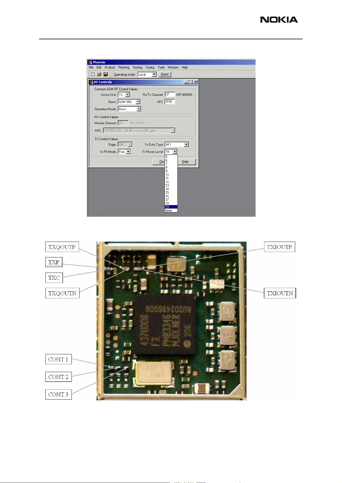
NEM-4 Company Confidential
6 - Troublehsooting Instructions Nokia Customer Care
Figure 28: Mjoelner Can Tx Test Points
Page 6-78 Copyright © 2004 Nokia Corporation Issue 2 09/2004
Company Confidential
Page 79
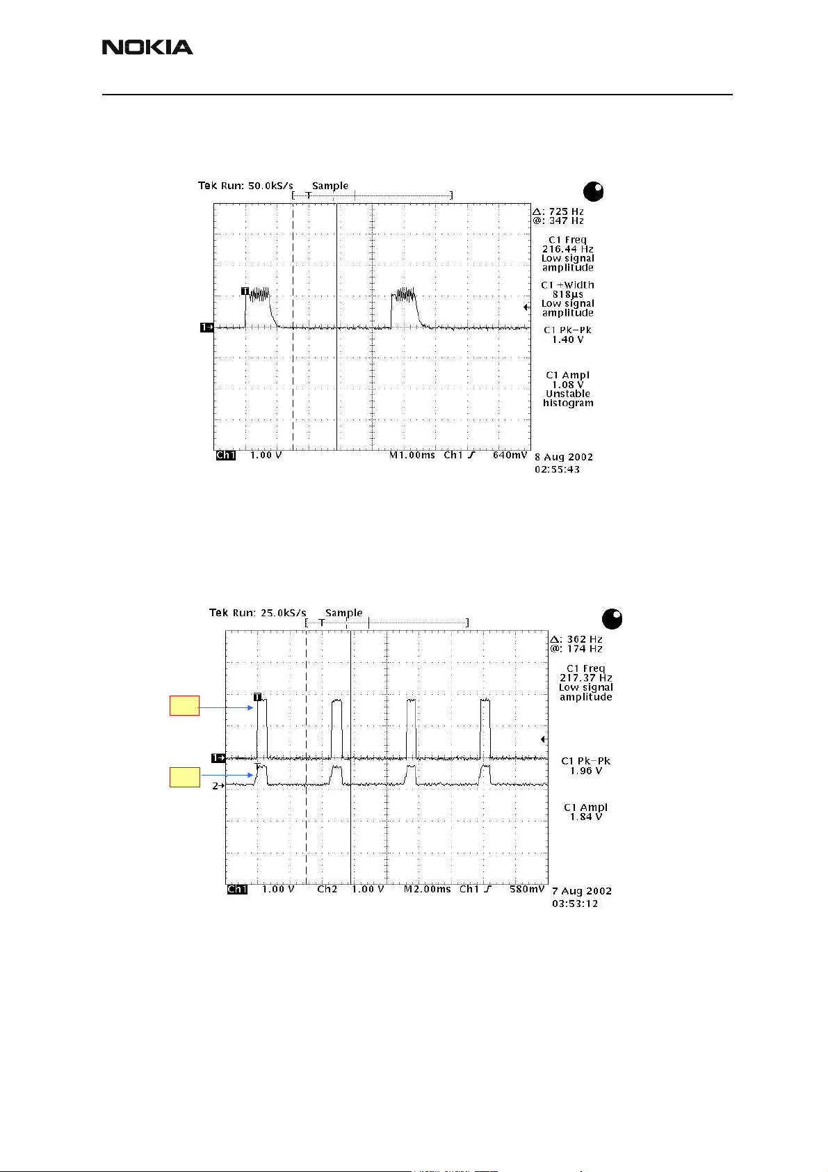
Company Confidential NEM-4
Nokia Customer Care 6 - Troublehsooting Instructions
TX Analog I & Q Data, C715 & C716
TXP
TXC
TXP & TXC Lines during Transmission
Issue 2 09/2004 Copyright © 2004 Nokia Corporation Page 6-79
Company Confidential
Page 80
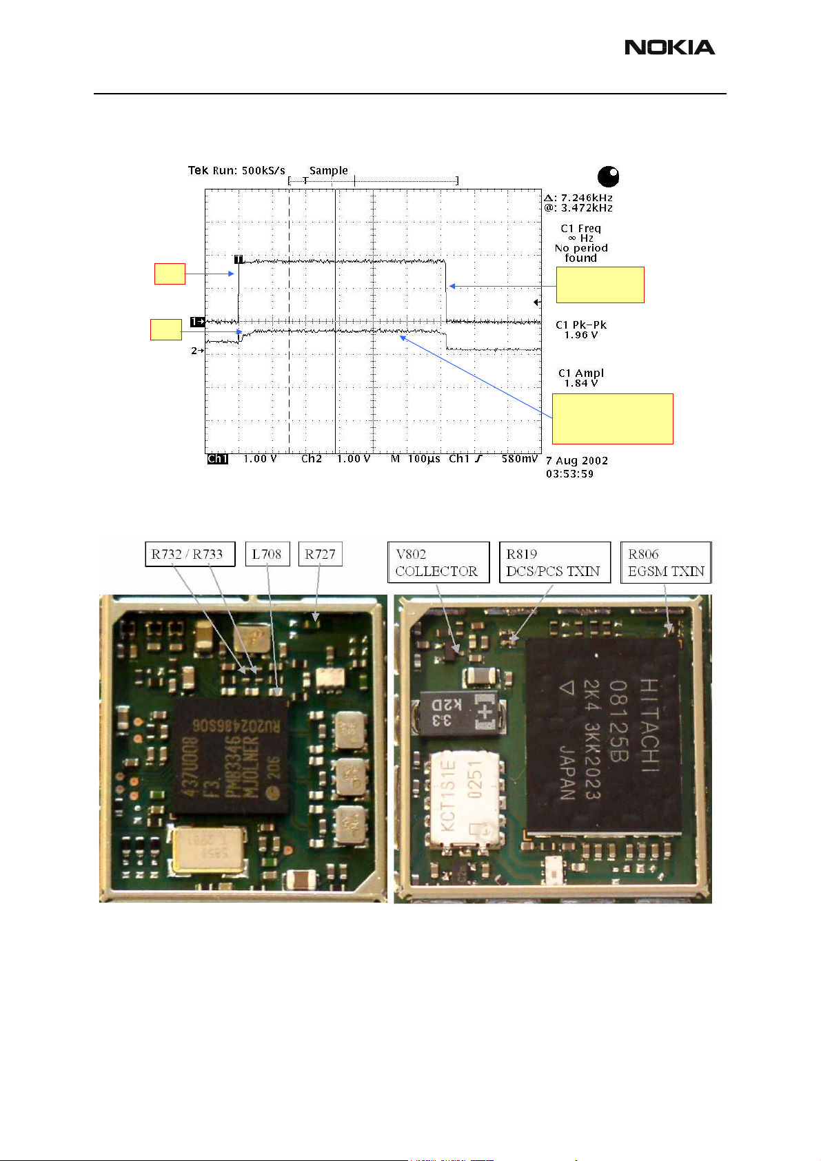
NEM-4 Company Confidential
6 - Troublehsooting Instructions Nokia Customer Care
TXP / TXC Mask
TXP
TXC
Power Control
Loop On
Baseband Generated
Reference for EGSM
Power Level 19
Figure 29: EGSM TX Can Test Points
Page 6-80 Copyright © 2004 Nokia Corporation Issue 2 09/2004
Company Confidential
Page 81

Company Confidential NEM-4
Nokia Customer Care 6 - Troublehsooting Instructions
VTXB_900 (EGSM V802 Pre-Amp Biasing Waveform)
Only Biases V802 for
duration of TX Pulse.
EGSM Transmit Waveform (Burst, Power Level 19)
Phone drew 140mA during Burst operation
Issue 2 09/2004 Copyright © 2004 Nokia Corporation Page 6-81
Company Confidential
Page 82

NEM-4 Company Confidential
6 - Troublehsooting Instructions Nokia Customer Care
EGSM Transmit Waveform (Continuous, Power Level 19)
**Was drawing over 600mA during continuous operation**
TX path of the transmitted EGSM900 signal
For easy error tracing it is important to know the signal path of the EGSM900 transmitter. The components can be grouped into blocks and drawn as shown below. Note that
the following picture shows both EGSM900 transmitter (bottom) and GSM1800/
GSM1900 transmitter (top).
Page 6-82 Copyright © 2004 Nokia Corporation Issue 2 09/2004
Company Confidential
Page 83
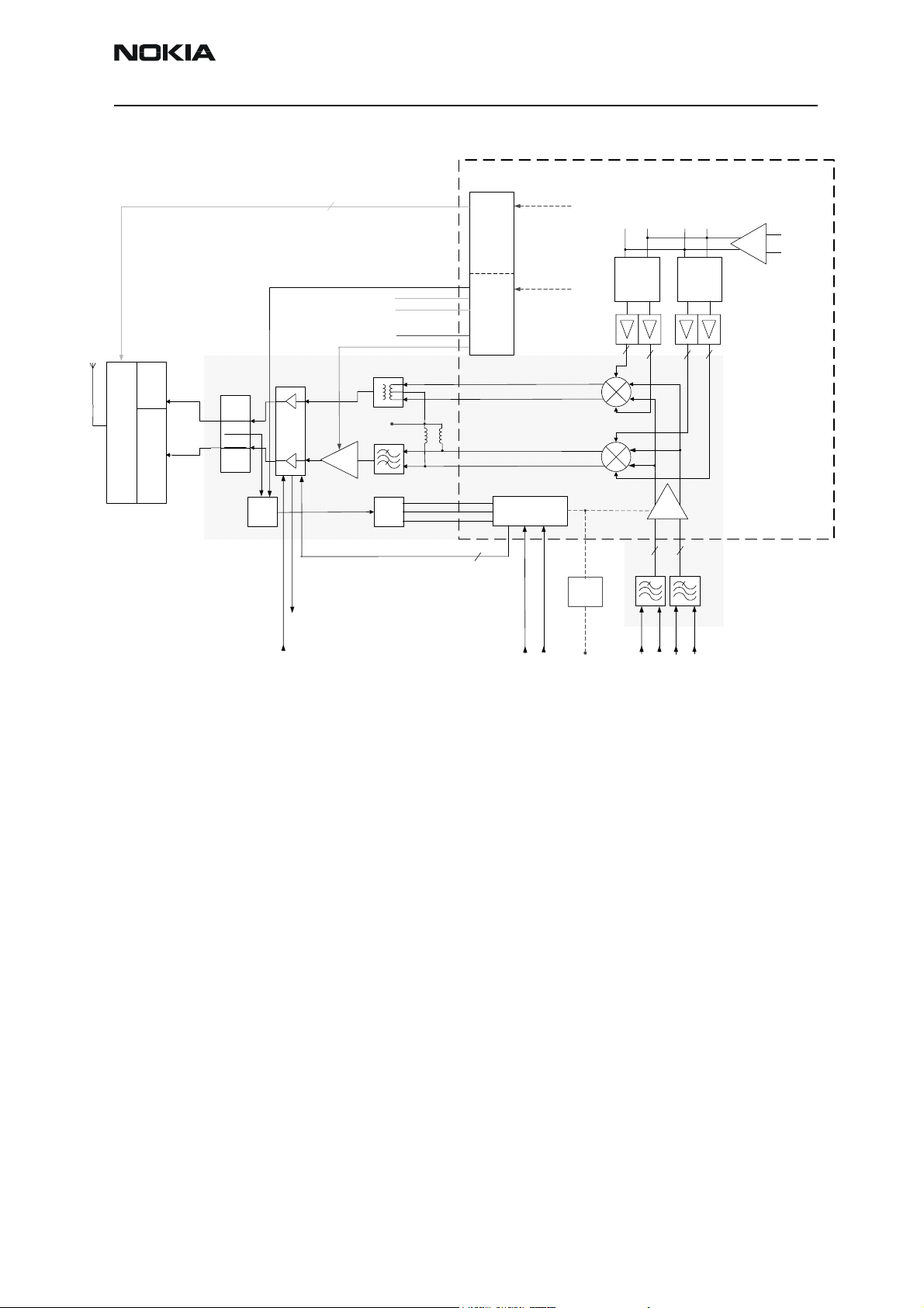
Company Confidential NEM-4
Nokia Customer Care 6 - Troublehsooting Instructions
VANTL / VANTM / VANTH
3
VB_DET
VTXLOL
VTXLOH
VTXBH
VTXBL
PCN/PCS
GSM
TX
PCN
Ant Switch
TX
PCS
Dir. Coupler
PA
Buffer
EGSM
DET
PA_IDENT
VBATTRF
VTX
Balun
SAW
PWloop
filter
OUTHP
OUTHM
OUTLP
OUTLM
DET
PLFB1
PLFB2
VPCH/VPCL
RF
Controls
RF
Controls
Open
collector
Open
collector
2
PWC
TXP
VDDDIG
VDDRXBB
1/2
2
2
1/4
2
2
Mjølner
TXC
TXP
TXC
VDDTX
Supply
filter
VTX
VR2
2
2
TXQP/TXQM
TXIP/TXIM
EGSM900 TX path of Mjoelner RF ASIC
The balanced TX IQ signal is provided by the base band and is coming to the Mjoelner RF
ASIC. The TX paths of the Mjoelner RF ASIC include mainly two RF modulators for upconversion of the base band signals, one for EGSM900 and one common for GSM1800/
GSM1900. The base band signal is modulated with the LO signal corresponding to the
wanted TX channel. The GSM TX output of the Mjoelner RF ASIC is a balanced signal.
From the output of the Mjoelner RFASIC the signal is fed through the EGSM TX SAW filter (balanced to single-ended), a 900MHz buffer, and a 5-db pad to the PA EGSM input.
EGSM900 TX path of the Power Amplifier (PA)
The PA EGSM900 part has a maximum output power of app. 35dBm. Voltage supply is
coming directly from the Battery connectors.
The EGSM900 output is controlled by the power control loop. From the EGSM900 output
of the PA the RF signal is fed through the directional coupler (one of the power control
loop components) to the antenna switch.
Antenna switch (TX/RX switch)
The antenna Switch works as a diplexer for the RX and TX signals. Moreover, it suppresses the TX harmonics generated by the PA. The antenna switch is controlled by the
Mjoelner RF ASIC using the control signals CONT1, CONT2 and CONT3. The following
Issue 2 09/2004 Copyright © 2004 Nokia Corporation Page 6-83
Company Confidential
Page 84
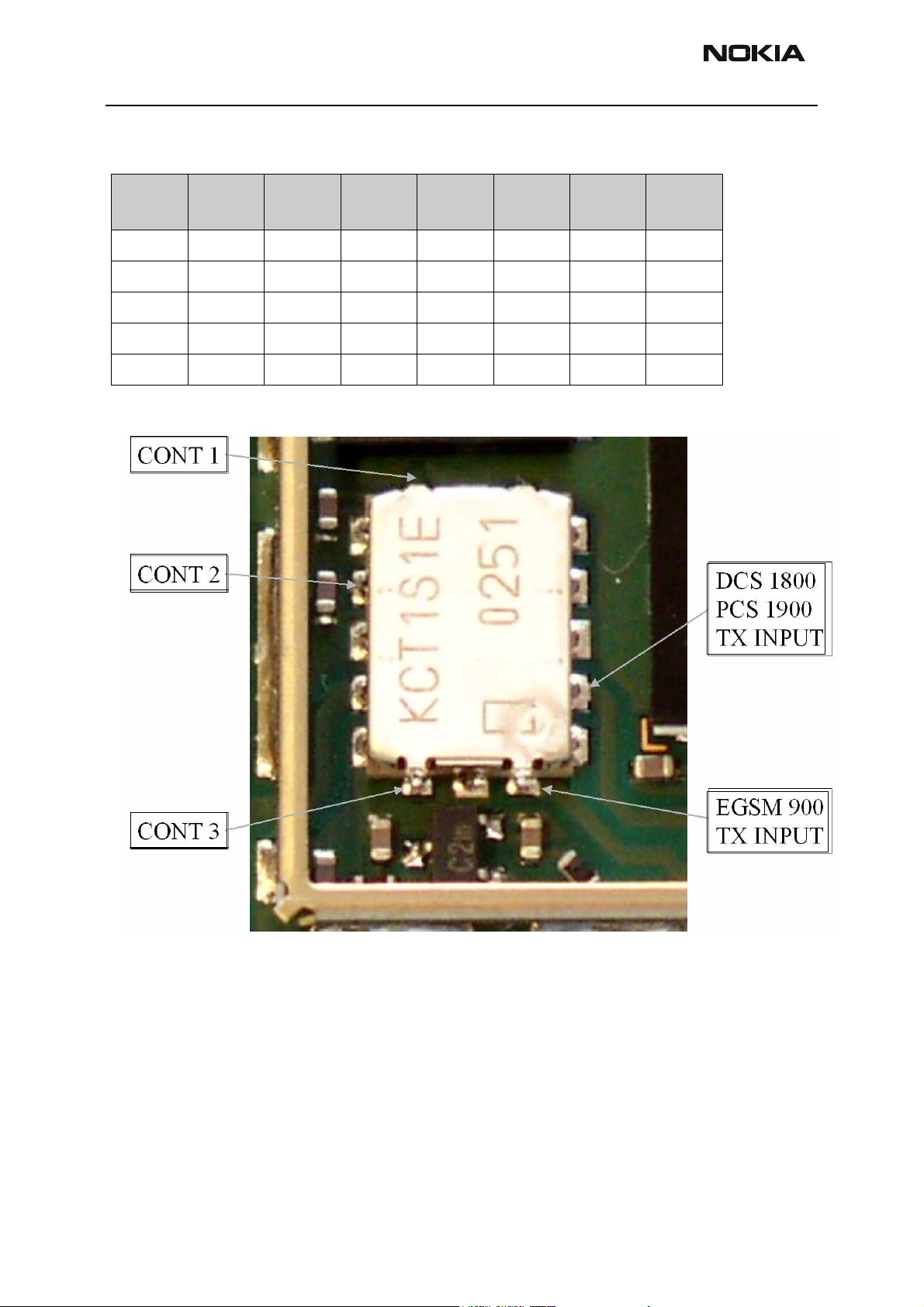
NEM-4 Company Confidential
6 - Troublehsooting Instructions Nokia Customer Care
table shows the possible different states.
CONT1
[Volt]
0 0 0 X
0 0 0 X
0 0 2.7 X
0 2.7 0 X
2.7 0 0 X
CONT2
[Volt]
CONT3
[Volt]
EGSM
Rx
Figure 30: Antenna Switch Test Points
DCS Rx PCS Rx EGSM Tx
DCS/PCS
Tx
Page 6-84 Copyright © 2004 Nokia Corporation Issue 2 09/2004
Company Confidential
Page 85
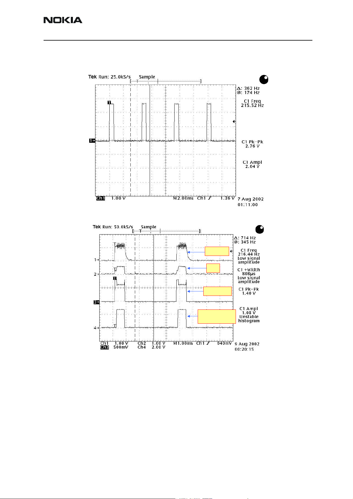
Company Confidential NEM-4
Nokia Customer Care 6 - Troublehsooting Instructions
Antenna Switch Control Line (CONT3) During EGSM Transmission
Antenna Switch Control Line During EGSM Transmission
EGSM Tx fault finding flow chart
THE FIRST FLOW DIAGRAM ASSUMES THE FOLLOWING:
Transmit Timing
TXIOUTP
TXC
VTXB_900
Antenna Switch
CONT 3
• Phoenix has been set up as shown on page 24 (the Tx power level may be
increased using Phoenix if it makes the Tx pulse easier to see).
• Relevant components have been visually inspected for orientation, placement,
etc.
• The transmit signal has been checked with a spectrum analyzer at RF connector,
X602 and was found to be too low or non-existent.
Issue 2 09/2004 Copyright © 2004 Nokia Corporation Page 6-85
Company Confidential
Page 86

NEM-4 Company Confidential
6 - Troublehsooting Instructions Nokia Customer Care
• The VCO is running correctly.
• The power amplifier is getting a correct VBATRF supply via L805 & L809.
• Mjoelner’s supply voltages VR1A, VR2, VR3, VR4, VR5 & VR7 are all working correctly.
Change
L801
Is Signal at
Antenna pin
of Z601 ok?
Change X602
RF Connector
YES
Change
Antenna
Switch
Is Signal at
TX_GSM on
L801 OK?
YES
Check Antenna
Switch Control
Lines. Do they
match the results
in the table?
Check L701,
L702 & L703.
OK?
Replace
Inductors
NO
Is Signal
at C834
OK?
YES
NO
Probe VPD_900Signal
on R818 and set Power
Level to 19 using Phoenix.
Is Pulse Pk-Pk 2.8V?
NO
NO
YES
NO
KEY
Test using
Spectrum Analyzer
START
YESYESNO NO NO
Is EGSM
TXIN signal
at R805 OK?
R 806
YES
NO
YES
Is Signal at V802
Collector OK?
Is VTXB
_900 OK?
NO
Is Signal at
C733 OK?
R
Is signal at
L807 OK?
YES NO
NO
YES
YES
Are TX I & Q on
C715 & C716. OK?
YES
Are TXP &
TXC visible?
YES
NO
TXP
Is VR2
2.8V on
C731?
NO YES
NO
TXC
Replace PA
Check / Replace
R805, C820, C821
R 806
Test using
Oscilloscope
Check Z701 &
Biasing components
Check V802 &
associated components
Check /
Inspect
End
Action
Change
Mjoelner
Change UEM?
Are digital I & Q
OK?
signals OK on
J123 & J214?
YES
NO
Change
UPP
Change
UEM
General instructions for GSM1800/1900 TX Troubleshooting
Apply an RF-cable to the RF-connector to allow the transmitted signal to act as normal.
RF-cable should be connected to measurement equipment (GSM Test equipment, Powermeter, Spectrum Analyzer, or similar).
DCS 1800/PCS 1900 Tx fault finding flow chart
The following diagram assumes the following:
• Phoenix has been set up as shown previously (selecting DCS 1800 in the RF control box).
• Relevant components have been visually inspected for orientation, placement
etc.
• The Transmit Signal has been checked with a Spectrum Analyzer at the RF connector, X602 and was found to be low or non-existent.
• The VCO is running correctly.
• The Power Amplifier is getting a correct VBATRF supply via L805 & L809.
Page 6-86 Copyright © 2004 Nokia Corporation Issue 2 09/2004
Company Confidential
Page 87
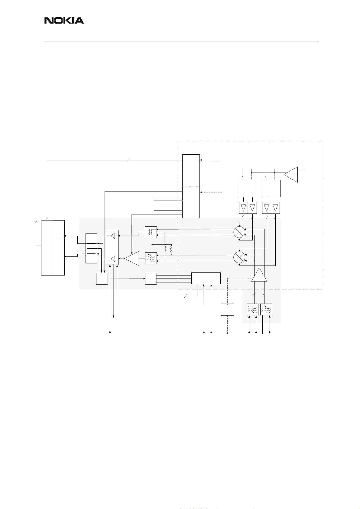
Company Confidential NEM-4
Nokia Customer Care 6 - Troublehsooting Instructions
• Mjoelner’s supply voltages VR1A, VR2, VR3, VR4, VR5 & VR7 are all working correctly.
Path of the transmitted GSM1800/1900 signal
For easy error tracking it is important to know the signal path of the GSM1800/
GSM1900 transmitter. The components can be grouped into blocks and drawn as shown
below. Note that the picture shows both EGSM transmitter (bottom) and GSM1800/
GSM1900 transmitter (top).
VANTL / VANTM / VANTH
3
VB_DET
VTXLOL
VTXLOH
VTXBH
VTXBL
PCN/PCS
GSM
TX
PCN
Ant Switch
TX
PCS
Dir. Coupler
PA
VTX
Buffer
EGSM
DET
PA_IDENT
VBATTRF
Balun
SAW
PWloop
filter
OUTHP
OUTHM
OUTLP
OUTLM
DET
PLFB1
PLFB2
VPCH/VPCL
RF
Controls
RF
Controls
Open
collector
Open
collector
2
PWC
TXP
TXP
TXC
TXC
VDDDIG
VDDRXBB
VDDTX
Supply
filter
VTX
VR2
1/2
2
2
1/4
2
2
Mjølner
2
2
TXQP/TXQM
TXIP/TXIM
The path of Mjoelner RF ASIC
The balanced TX IQ signal from base band is coming to Mjoelner RF ASIC. The GSM1900
path includes an common RF modulator for GSM1800 and GSM1900. The BB signal is
up-converted with the LO signal corresponding to the wanted TX channel. The GSM1800/
GSM1900 TX output of Mjoelner is a balanced signal.
From the output of Mjoelner the signal is fed through the Balun T701 (Balanced to single
ended) and an 3 dB pad to the PA GSM1800/1900 input.
The path of the PA
The GSM1800/GSM1900 part of the PA has a maximum output of app. 33dBm. The sup-
Issue 2 09/2004 Copyright © 2004 Nokia Corporation Page 6-87
Company Confidential
Page 88
NEM-4 Company Confidential
6 - Troublehsooting Instructions Nokia Customer Care
ply is coming directly from the Battery connectors.
The output is controlled by the power control loop. From the output of the PA the signal
goes through the directional coupler (one of the power control loop components) to the
Antenna Switch.
Antenna Switch
The Antenna Switch works as a diplexer between RX and TX Bands. Moreover, it partly
suppresses the harmonics generated by the PA. Mjoelner RF ASIC controls the antenna
switch by three voltages CONT1, CONT2 and CONT3. The following table shows the different states.
CONT1
[Volt]
0 0 0 X
0 0 0 X
0 0 2.7 X
0 2.7 0 X
2.7 0 0 X
CONT2
[Volt]
CONT3
[Volt]
EGSM Rx DCS Rx PCS Rx EGSM Tx
DCS/PCS
Tx
Page 6-88 Copyright © 2004 Nokia Corporation Issue 2 09/2004
Company Confidential
Page 89
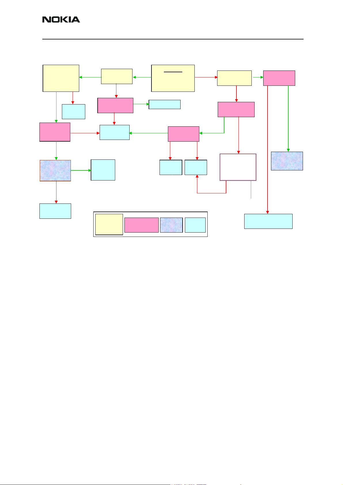
Company Confidential NEM-4
Nokia Customer Care 6 - Troublehsooting Instructions
Fault finding chart for GSM1800/GSM1900 transmitter
Is signal at
DCS / PCS
Input of Z601
OK?
Replace
L801
Are Z601
Control lines
as per table?
YES
Check RF
Connector
X602. OK?
NO
Replace RF
Connector.
NO
NOYES
YES
Is signal on
C823 OK?
Is VPD_1800
signal OK?
Investigate
Mjoelner
Replace
Antenna
Switch
KEY
Test With
Spectrum
Analyzer
NO
NO
Test With
Oscilloscope
YES
YES
Replace PA
START
Is TX Signal at
DCS / PCS In on
R819 OK?
YES
Are TXP &
TXC OK?
TXC
U/S
Change
UEM
Change
UPP
Check /
Inspect
NOYES
TXP
U/S
End
Action
Is TX Signal
at L705 OK?
NO
Are TX I & Q
Signals OK?
YES
Are Digital
Change UEM.
I & Q Signals
OK at J213 &
OK?
J214
NO YES
YES
Is Vr2 2.8V
on R720?
NO YES
NO
Refer To Baseband
Fault Finding
Check T701
& Associated
Components.
If the Tx output is too high, then it is most likely that there is a problem within the Power
Control loop.
Mjoelner is receiving the Reference TXC from Baseband and not getting any feedback
from DET to compare with TXC. The result is that Mjoelner drives VDP_900/VPD_1800
high to try and increase the power output so that the DET signal is matching TXC. With a
break in the Power Control loop, the DET signal never reaches Mjoelner so it assumes
that the PA is not outputting enough power so it tries to compensate by increasing the
gain.
When checking the Power Control loop, make sure that (C803) is pulsing at 2.8V Peak to
Peak. Check the DET pulse at Mjoelner input on R706.
Issue 2 09/2004 Copyright © 2004 Nokia Corporation Page 6-89
Company Confidential
Page 90
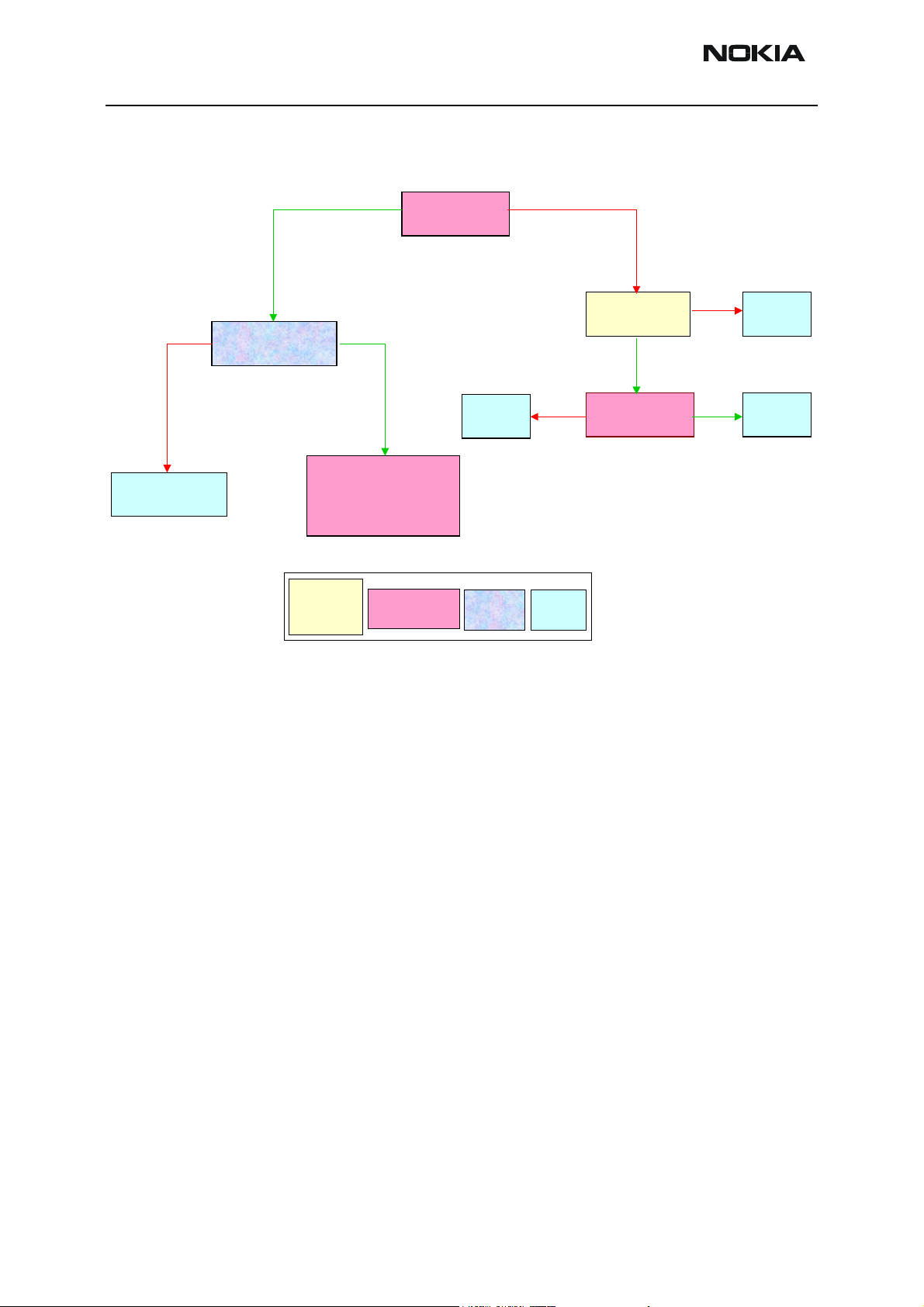
NEM-4 Company Confidential
6 - Troublehsooting Instructions Nokia Customer Care
This case is the same for EGSM, DCS1800 & DCS1900.
NO YES
Replace Faulty
Components
Are R706, R707
& R708 OK?
Eunsure that VBD
is pulsing 2.8V
Pk - PK and
investigate Mjoelner
KEY
Test With
Spectrum
Analyzer
Is DET Pulse
on C805 OK?
Test With
Oscilloscope
Replace
V801
Check /
Inspect
NOYES
NO
End
Action
Is RF Signal
at V801 OK?
YES
Is DET Pulse
on C804 OK?
NO
YES
Replace
L801
Replace
R802
Page 6-90 Copyright © 2004 Nokia Corporation Issue 2 09/2004
Company Confidential
Page 91

Company Confidential NEM-4
Nokia Customer Care 6 - Troublehsooting Instructions
NEM-4 Synthesizer
There is only one PLL synthesizer generating frequencies for both Rx and Tx for all three
bands (EGSM900, GSM1800 and GSM1900). VCO frequency is divided by 2 or by 4 in
Mjoelner depending on which band is active.
General instructions for synthesizer troubleshooting
Connect the phone to a PC with DAU-9P cable and dongle and follow these instructions:
Start Phoenix Service Software (dongle needed):
Open FBUS connection
Select Scan Product Ctrl-R
or File Alt-F
Scan Product P
Wait until phone information shows in the lower right corner of the screen.
Set operating mode to local mode.
Start RF Control window:
Select Testing Alt-S
RF Controls R
Wait until the RF Controls window pops up
Set the synthesizer to the following mode:
Select Band GSM 900
Active unit RX
Operation mode Continuous
RX/TX Channel 37
Issue 2 09/2004 Copyright © 2004 Nokia Corporation Page 6-91
Company Confidential
Page 92

NEM-4 Company Confidential
6 - Troublehsooting Instructions Nokia Customer Care
The setup should now look like this:
Since VCO chamber is completely shielded, it is not easy to measure frequency of
3769.6MHz at the output of the VCO (G701) using a resistive probe and a spectrum analyzer. It is possible to measure tuning voltage at charge pump output (C710) easily. For
f
= 3769.6MHz the tuning voltage should be 2.3VDC .. 2.8VDC (Tuning sensitivity of
VCO
VCO is 240MHz/V typ.).
Page 6-92 Copyright © 2004 Nokia Corporation Issue 2 09/2004
Company Confidential
Page 93

Company Confidential NEM-4
Nokia Customer Care 6 - Troublehsooting Instructions
Figure 31: PLL Synthesizer Test Points
If this is not the case, then go to Fault finding chart in this document for Troubleshooting.
Figure 32: Mjoelner Can Test Points
Issue 2 09/2004 Copyright © 2004 Nokia Corporation Page 6-93
Company Confidential
Page 94

NEM-4 Company Confidential
6 - Troublehsooting Instructions Nokia Customer Care
26 MHz reference oscillator (VCXO)
The 26 MHz reference oscillator (VCXO) is part of Mjoelner RF-ASIC (N601). It needs only
an external 26 MHz Xtal (B601) as external circuitry.
The reference oscillator has three functions:
• Reference frequency for the PLL synthesizer.
• System clock for BB (RFCLK_I = 26 MHz).
• 26 MHz Reference clock (LPRFCLK_I) for Bluetooth Module (N430) via buffer
V601.
For an error free initial synchronization, the 26MHz frequency of the VCXO must be
accurate enough. Therefore, a VCXO-calibration (cal) value is written via the serial Bus
into the RefOSCCAL register of Mjoelner and an additional bit in the RefOSCCntl register
of the Mjoelner. That is necessary for the rough calibration of the VCXO.
The VCXO is fine tuned by programming the AFC value via the serial bus of Mjoelner. The
necessary AFC value is written into the RefOSCAFC register in Mjoelner.
VCO
The VCO is able to generate frequencies in the range from 3420MHz to 3980MHz when
PLL is in function. The frequency of the VCO signal is divided by 2 or by 4 in Mjoelner RFASIC. So it is possible to generate the frequency of all channels in EGSM900, GSM1800
and GSM1900 (both RX and TX). Frequency of the VCO is controlled by DC voltage (Vc)
coming from the PLL loop filter. Range of Vc when PLL is in function is 0.7V– 3.8V. Typical tuning sensitivity of the VCO is 240MHz/V. Even if PLL is not working (Vc out of
range) there is a frequency at the output of the VCO, which is between 3 and 4 GHz (if
the VCO itself is ok).
Page 6-94 Copyright © 2004 Nokia Corporation Issue 2 09/2004
Company Confidential
Page 95
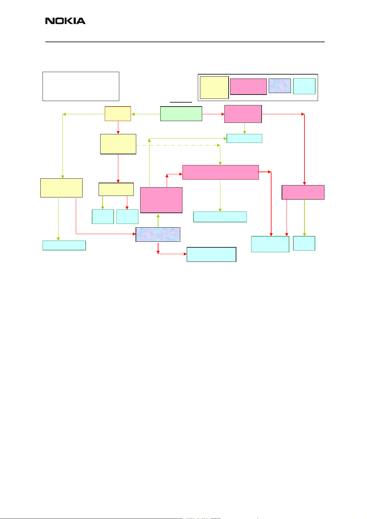
Company Confidential NEM-4
Nokia Customer Care 6 - Troublehsooting Instructions
Fault finding chart for PLL synthesizer
Set up Phoenix RF Controls
Band: GSM 900
Mode: RX Continuous
Channel: 37
Check T702
Balanced O/P.
Signal same?
YES NO
Change Channel
to 975. Does LO
change frequency?
YES
NO
Check T702 I/P.
LO Present?
YES NO
Change
T702
PLL is working
Is LO@
3.77 GHz
NO
Change
R731
START
YES
Check VCO Out.
Is LO visible?
YES
YES NO
Does the VC
Vge change
when you change
channels?
YES
Check Loop Filter
Components. OK?
NO
KEY
Test with
Spectrum
Analyzer
NOYES
Check Mjoelner Voltage Supplies
VR1A, VIO, VR3, VREF1. OK?
Test with
Oscilloscope
Check VR7 VCO
Side of R730.
Vge OK?
Replace G701
YES
YES
Replace Mjoelner
Replace Faulty Loop
Filter Components
Check /
Inspect
NO
NO
Refer to BB
Fault Finding
End
Action
Check VR7 J618.
Vge OK?
NO
YES
Change
R730
It is important to say that power supply for VCXO ( VR3) is only switched ‘OFF’ in the socalled ‘Deep Sleep Mode’ and power supply for VCO (G701 VR7) is switched ‘OFF’ in socalled ‘Sleep Mode’.
Issue 2 09/2004 Copyright © 2004 Nokia Corporation Page 6-95
Company Confidential
Page 96
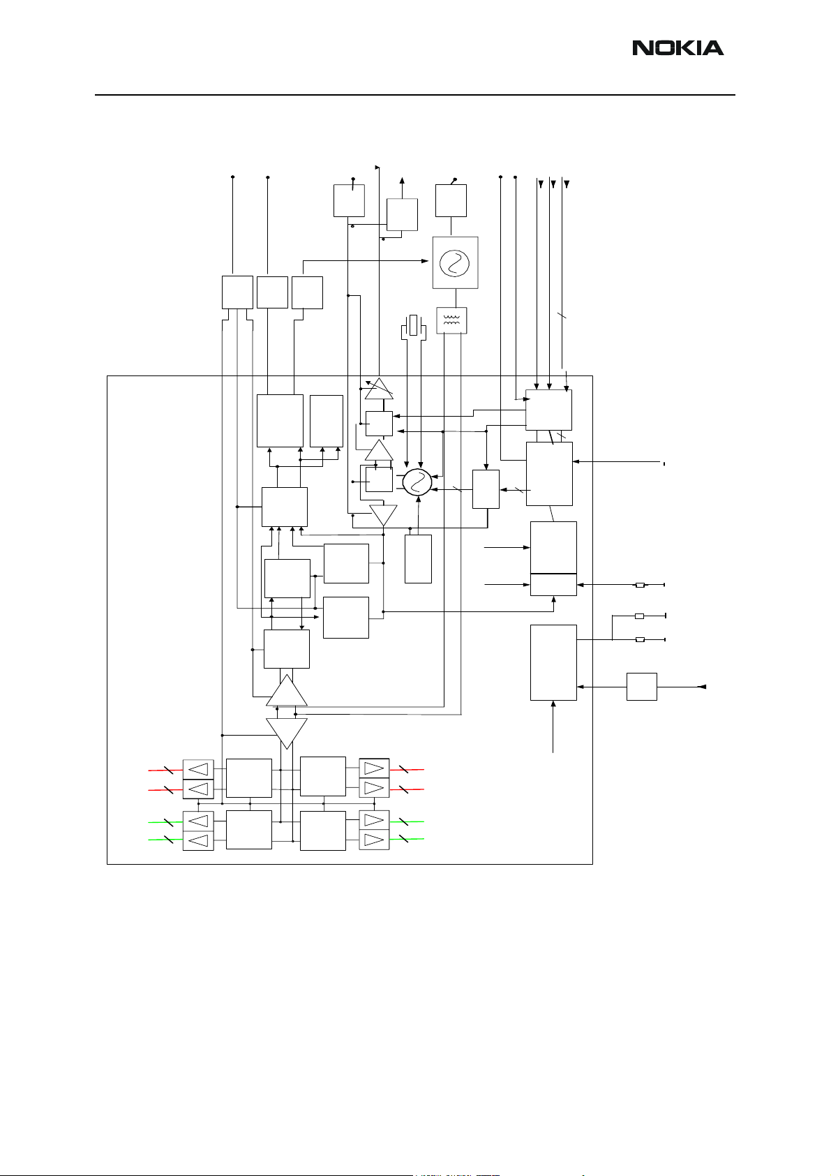
NEM-4 Company Confidential
6 - Troublehsooting Instructions Nokia Customer Care
PLL block diagram
VR5
VR1A
5V
VPLL
Vcp
filter
filter
Synth
supply
VDDLO
VDDPRE
VDDPLL
supply
VDDCP
Charge
PLL
loop
CPOUT
Pump
ϕ
NDIV
ADIV
64/65
VR3
filter
supply
VCXO
REFOUT
LPR
CLK
buffer
filter
VDDXO
REFOUT
VDDBBB
XTALM
Buffer
Lock
Detect
LOCNT
1/2
Buf/
AGC
RDIV
REFCNT
VCXO Bias
VR7
filter
VCO
supply
26MHz
INPLO
INMLO
XTALP
RESETX
R2H/R2
VIO
VIO
VBB (1.8V)
VDDDL
VDDTX
VDDRXBB
Ref clk set
SELADDR
GENIO6
RFBUSX
RFBUSDA
RESET_X
RESETX
I/O level
Digital Co ntrol
Sensor
RFBUSCLK
RF BUS CLK
RF BUS ENI
RF BUS DA
3
RF_EN
RF_CLK
RF_DATA
RF BUS CLK
RF BUS ENX
RF BUS DA
shift
3
VCOSENSE
BIST / Temp.
SENSE
RBEXT
Rpa
PA vendor
3.3n
2,7k
indication
VR2
VDDDIG
Control
AFC/CAL
Main Bias Circuit
Resistor Ext/R2H/R2
VDDRXBB
mixer
To GSM RX
2 2 2 2
RX mixer
To DCS/PCS
1/2 1/4
1/2 1/4
To GSM
Modulator
2 2 2 2
Modulator
To DCS/PCS
VBEXT
Ref.
filter
VREF1
RFCONV_0(9)
Page 6-96 Copyright © 2004 Nokia Corporation Issue 2 09/2004
Company Confidential
Page 97
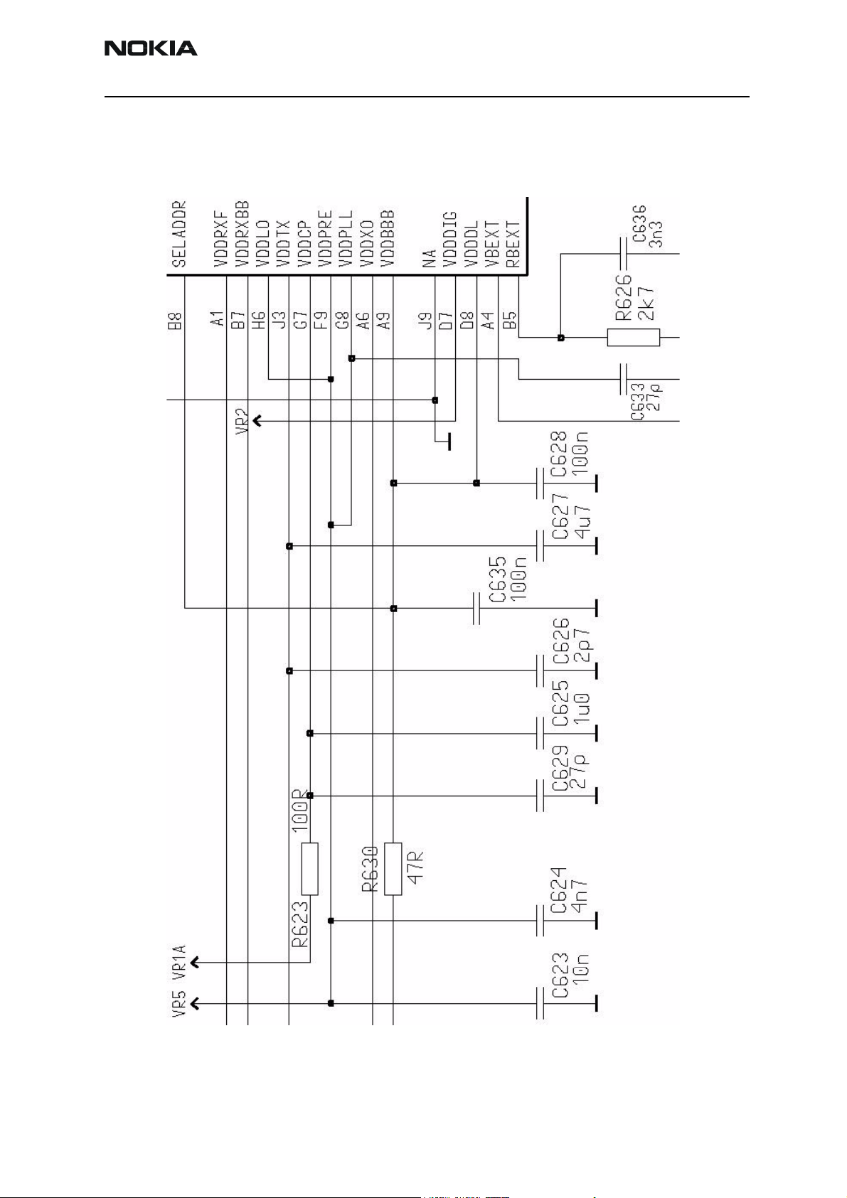
Company Confidential NEM-4
Nokia Customer Care 6 - Troublehsooting Instructions
PLL power supply
Issue 2 09/2004 Copyright © 2004 Nokia Corporation Page 6-97
Company Confidential
Page 98
NEM-4 Company Confidential
6 - Troublehsooting Instructions Nokia Customer Care
Loop filter
VCO and power supply
Page 6-98 Copyright © 2004 Nokia Corporation Issue 2 09/2004
Company Confidential
Page 99
Company Confidential NEM-4
Nokia Customer Care 6 - Troublehsooting Instructions
26MHz Bluetooth buffer
Issue 2 09/2004 Copyright © 2004 Nokia Corporation Page 6-99
Company Confidential
Page 100

NEM-4 Company Confidential
6 - Troublehsooting Instructions Nokia Customer Care
Frequency lists
EGSM900
CH TX RX VCO TX VCO RX CH TX RX VCO TX VCO RX CH TX RX VCO TX VCO RX
975 880.2 925.2 3520.8 3700.8 1 890.2 935.2 3560.8 3740.8 63 902.6 947.6 3610.4 3790.4
976 880.4 925.4 3521.6 3701.6 2 890.4 935.4 3561.6 3741.6 64 902.8 947.8 3611.2 3791.2
977 880.6 925.6 3522.4 3702.4 3 890.6 935.6 3562.4 3742.4 65 903.0 948.0 3612.0 3792.0
978 880.8 925.8 3523.2 3703.2 4 890.8 935.8 3563.2 3743.2 66 903.2 948.2 3612.8 3792.8
979 881.0 926.0 3524.0 3704.0 5 891.0 936.0 3564.0 3744.0 67 903.4 948.4 3613.6 3793.6
980 881.2 926.2 3524.8 3704.8 6 891.2 936.2 3564.8 3744.8 68 903.6 948.6 3614.4 3794.4
981 881.4 926.4 3525.6 3705.6 7 891.4 936.4 3565.6 3745.6 69 903.8 948.8 3615.2 3795.2
982 881.6 926.6 3526.4 3706.4 8 891.6 936.6 3566.4 3746.4 70 904.0 949.0 3616.0 3796.0
983 881.8 926.8 3527.2 3707.2 9 891.8 936.8 3567.2 3747.2 71 904.2 949.2 3616.8 3796.8
984 882.0 927.0 3528.0 3708.0 10 892.0 937.0 3568.0 3748.0 72 904.4 949.4 3617.6 3797.6
985 882.2 927.2 3528.8 3708.8 11 892.2 937.2 3568.8 3748.8 73 904.6 949.6 3618.4 3798.4
986 882.4 927.4 3529.6 3709.6 12 892.4 937.4 3569.6 3749.6 74 904.8 949.8 3619.2 3799.2
987 882.6 927.6 3530.4 3710.4 13 892.6 937.6 3570.4 3750.4 75 905.0 950.0 3620.0 3800.0
988 882.8 927.8 3531.2 3711.2 14 892.8 937.8 3571.2 3751.2 76 905.2 950.2 3620.8 3800.8
989 883.0 928.0 3532.0 3712.0 15 893.0 938.0 3572.0 3752.0 77 905.4 950.4 3621.6 3801.6
990 883.2 928.2 3532.8 3712.8 16 893.2 938.2 3572.8 3752.8 78 905.6 950.6 3622.4 3802.4
991 883.4 928.4 3533.6 3713.6 17 893.4 938.4 3573.6 3753.6 79 905.8 950.8 3623.2 3803.2
992 883.6 928.6 3534.4 3714.4 18 893.6 938.6 3574.4 3754.4 80 906.0 951.0 3624.0 3804.0
993 883.8 928.8 3535.2 3715.2 19 893.8 938.8 3575.2 3755.2 81 906.2 951.2 3624.8 3804.8
994 884.0 929.0 3536.0 3716.0 20 894.0 939.0 3576.0 3756.0 82 906.4 951.4 3625.6 3805.6
995 884.2 929.2 3536.8 3716.8 21 894.2 939.2 3576.8 3756.8 83 906.6 951.6 3626.4 3806.4
996 884.4 929.4 3537.6 3717.6 22 894.4 939.4 3577.6 3757.6 84 906.8 951.8 3627.2 3807.2
997 884.6 929.6 3538.4 3718.4 23 894.6 939.6 3578.4 3758.4 85 907.0 952.0 3628.0 3808.0
998 884.8 929.8 3539.2 3719.2 24 894.8 939.8 3579.2 3759.2 86 907.2 952.2 3628.8 3808.8
999 885.0 930.0 3540.0 3720.0 25 895.0 940.0 3580.0 3760.0 87 907.4 952.4 3629.6 3809.6
1000 885.2 930.2 3540.8 3720.8 26 895.2 940.2 3580.8 3760.8 88 907.6 952.6 3630.4 3810.4
1001 885.4 930.4 3541.6 3721.6 27 895.4 940.4 3581.6 3761.6 89 907.8 952.8 3631.2 3811.2
1002 885.6 930.6 3542.4 3722.4 28 895.6 940.6 3582.4 3762.4 90 908.0 953.0 3632.0 3812.0
1003 885.8 930.8 3543.2 3723.2 29 895.8 940.8 3583.2 3763.2 91 908.2 953.2 3632.8 3812.8
1004 886.0 931.0 3544.0 3724.0 30 896.0 941.0 3584.0 3764.0 92 908.4 953.4 3633.6 3813.6
1005 886.2 931.2 3544.8 3724.8 31 896.2 941.2 3584.8 3764.8 93 908.6 953.6 3634.4 3814.4
1006 886.4 931.4 3545.6 3725.6 32 896.4 941.4 3585.6 3765.6 94 908.8 953.8 3635.2 3815.2
1007 886.6 931.6 3546.4 3726.4 33 896.6 941.6 3586.4 3766.4 95 909.0 954.0 3636.0 3816.0
1008 886.8 931.8 3547.2 3727.2 34 896.8 941.8 3587.2 3767.2 96 909.2 954.2 3636.8 3816.8
1009 887.0 932.0 3548.0 3728.0 35 897.0 942.0 3588.0 3768.0 97 909.4 954.4 3637.6 3817.6
1010 887.2 932.2 3548.8 3728.8 36 897.2 942.2 3588.8 3768.8 98 909.6 954.6 3638.4 3818.4
1011 887.4 932.4 3549.6 3729.6 37 897.4 942.4 3589.6 3769.6 99 909.8 954.8 3639.2 3819.2
1012 887.6 932.6 3550.4 3730.4 38 897.6 942.6 3590.4 3770.4 100 910.0 955.0 3640.0 3820.0
1013 887.8 932.8 3551.2 3731.2 39 897.8 942.8 3591.2 3771.2 101 910.2 955.2 3640.8 3820.8
1014 888.0 933.0 3552.0 3732.0 40 898.0 943.0 3592.0 3772.0 102 910.4 955.4 3641.6 3821.6
1015 888.2 933.2 3552.8 3732.8 41 898.2 943.2 3592.8 3772.8 103 910.6 955.6 3642.4 3822.4
1016 888.4 933.4 3553.6 3733.6 42 898.4 943.4 3593.6 3773.6 104 910.8 955.8 3643.2 3823.2
1017 888.6 933.6 3554.4 3734.4 43 898.6 943.6 3594.4 3774.4 105 911.0 956.0 3644.0 3824.0
1018 888.8 933.8 3555.2 3735.2 44 898.8 943.8 3595.2 3775.2 106 911.2 956.2 3644.8 3824.8
1019 889.0 934.0 3556.0 3736.0 45 899.0 944.0 3596.0 3776.0 107 911.4 956.4 3645.6 3825.6
1020 889.2 934.2 3556.8 3736.8 46 899.2 944.2 3596.8 3776.8 108 911.6 956.6 3646.4 3826.4
1021 889.4 934.4 3557.6 3737.6 47 899.4 944.4 3597.6 3777.6 109 911.8 956.8 3647.2 3827.2
1022 889.6 934.6 3558.4 3738.4 48 899.6 944.6 3598.4 3778.4 110 912.0 957.0 3648.0 3828.0
1023 889.8 934.8 3559.2 3739.2 49 899.8 944.8 3599.2 3779.2 111 912.2 957.2 3648.8 3828.8
0 890.0 935.0 3560.0 3740.0 50 900.0 945.0 3600.0 3780.0 112 912.4 957.4 3649.6 3829.6
51 900.2 945.2 3600.8 3780.8 113 912.6 957.6 3650.4 3830.4
52 900.4 945.4 3601.6 3781.6 114 912.8 957.8 3651.2 3831.2
53 900.6 945.6 3602.4 3782.4 115 913.0 958.0 3652.0 3832.0
54 900.8 945.8 3603.2 3783.2 116 913.2 958.2 3652.8 3832.8
55 901.0 946.0 3604.0 3784.0 117 913.4 958.4 3653.6 3833.6
56 901.2 946.2 3604.8 3784.8 118 913.6 958.6 3654.4 3834.4
57 901.4 946.4 3605.6 3785.6 119 913.8 958.8 3655.2 3835.2
58 901.6 946.6 3606.4 3786.4 120 914.0 959.0 3656.0 3836.0
59 901.8 946.8 3607.2 3787.2 121 914.2 959.2 3656.8 3836.8
60 902.0 947.0 3608.0 3788.0 122 914.4 959.4 3657.6 3837.6
61 902.2 947.2 3608.8 3788.8 123 914.6 959.6 3658.4 3838.4
62 902.4 947.4 3609.6 3789.6 124 914.8 959.8 3659.2 3839.2
Page 6-100 Copyright © 2004 Nokia Corporation Issue 2 09/2004
Company Confidential
 Loading...