

Page 1

Nokia Customer Care
7 - RF Description and
Troubleshooting
Issue 1 09/04 COMPANY CONFIDENTIAL
Copyright © 2004 Nokia. All Rights Reserved.
Page 2

RA-2/3
Nokia Customer Care
[This page intentionally blank]
Issue 1 09/04 COMPANY CONFIDENTIAL 2
Copyright © 2004 Nokia. All Rights Reserved.
Page 3

RA-2/3
7 - RF Description and Troubleshooting Nokia Customer Care
Table of Contents
Page No
CMT RF................................................................................................................. 5
Top-level description.......................................................................................... 5
RA-2 test point locations................................................................................... 6
Test points ......................................................................................................... 8
RF implementation in RA-2/3........................................................................... 11
Frequency plan ..............................................................................................11
RF block diagram ...........................................................................................12
Antenna switch module (ASM) .......................................................................12
DC characteristics ..........................................................................................13
Regulators................................................................................................. 13
DC supply currents.................................................................................... 13
Typical current consumption...................................................................... 14
Power distribution diagram........................................................................ 15
RF characteristics ............................................................................................ 16
Channel numbers and frequencies ................................................................ 16
RF Troubleshooting..........................................................................................17
Receiver description and troubleshooting........................................................ 17
Rx front end ...................................................................................................17
Antenna .........................................................................................................17
Receiver characteristics .................................................................................18
General instructions for Rx troubleshooting ...................................................19
Troubleshooting diagram for GSM850 receiver......................................... 23
Troubleshooting diagram for GSM900 receiver......................................... 24
Troubleshooting diagram for GSM1800 receiver....................................... 25
Troubleshooting diagram for GSM1900 receiver....................................... 26
Transmitter description and troubleshooting.................................................... 27
Power amplifier ..............................................................................................27
RF ASIC Helgo ..............................................................................................27
AFC function ..................................................................................................28
Transmitter characteristics .............................................................................28
General instructions for Tx troubleshooting ................................................... 28
Transmitter troubleshooting diagram......................................................... 30
HELGO IC troubleshooting diagram.......................................................... 31
PA and antenna switch troubleshooting diagram...................................... 32
Pictures of transmitter signals ................................................................... 33
Additional information for EDGE troubleshooting ............................................ 35
Transmitter EDGE troubleshooting diagram.............................................. 36
HELGO EDGE troubleshooting diagram................................................... 37
PA and antenna switch EDGE troubleshooting diagram........................... 38
Pictures of EDGE transmitter signals .............................................................39
Synthesizer description and troubleshooting................................................... 43
Frequency synthesizers .................................................................................43
General instructions for synthesizer troubleshooting .....................................43
Troubleshooting diagram for synthesizer .................................................. 44
Issue 1 09/04 COMPANY CONFIDENTIAL 3
Copyright © 2004 Nokia. All Rights Reserved.
Page 4

RA-2/3
7 - RF Description and Troubleshooting Nokia Customer Care
Table of Contents
Page No
Pictures of synthesizer signals.................................................................. 45
Frequency Lists ..............................................................................................48
GSM850 .................................................................................................... 48
GSM900 (including EGSM900)................................................................. 49
GSM1800 .................................................................................................. 50
GSM1900 .................................................................................................. 51
RF tunings after repairs ................................................................................... 52
WLAN RF Description....................................................................................... 53
RF operating modes ........................................................................................ 54
Transmitter .....................................................................................................54
Receiver .........................................................................................................55
Synthesizer .................................................................................................... 55
Antenna ..........................................................................................................55
Issue 1 09/04 COMPANY CONFIDENTIAL 4
Copyright © 2004 Nokia. All Rights Reserved.
Page 5

RA-2/3
7 - RF Description and Troubleshooting Nokia Customer Care
CMT RF
■ Top-level description
The RF module performs the necessary high frequency operations of the GSM850/EGSM900/
1800/1900 tripleband (EDGE) engine. Both the transmitter and receiver have been implemented by using direct conversion architecture which means that the modulator and demodulator
operate at the channel frequency.
The core of the RF is an application-specific integrated circuit, Helgo. Another core component
is a power amplifier module which includes two amplifier chains, one for GSM850/EGSM900
and the other for GSM1800/GSM1900.
Other key components include
• 26 MHz VCTCXO for frequency reference
• 3296-3980 MHz SHF VCO (super high frequency voltage controlled oscillator)
• Antenna switch module (ASM)
• Four SAW filters
The control information for the RF is coming from the baseband section of the engine through
a serial bus, referred later on as RFBus.
The whole RF circuitry is located on one side of the 8-layer PWB.
EMC leakage is prevented by using a metal cans. The RF circuits are separated into two
blocks.
• PA, ASM, LNA, baluns for Rx/Tx and Rx/Tx SAWs.
• Helgo RF IC, VCO + balun, VCTCXO, baluns and EGSM Rx filter
The RF transmission lines constitute of striplines and microstriplines after PA.
Issue 1 09/04 COMPANY CONFIDENTIAL 5
Copyright © 2004 Nokia. All Rights Reserved.
Page 6
RA-2/3
Nokia Customer Care 7 - RF Description and Troubleshooting
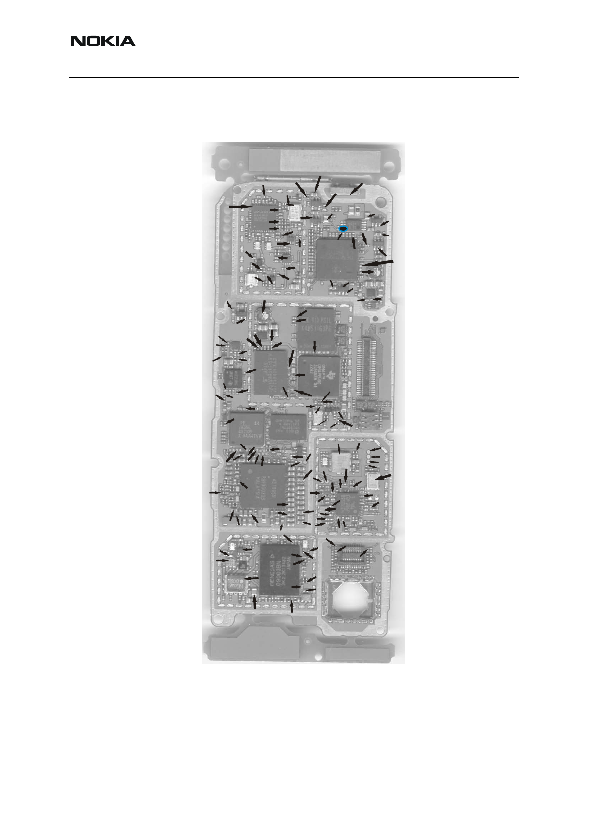
■ RA-2 test point locations
Figure 1: Top view
N6400
pins 39-42
C2104
C2105
R2106
C4104
R2125
L7830
Z7808
R6304
N6301
pin3
C4105
J2809
J2809
J8120
C2210
C6404
R6402
R6405
C5001
R5001
R4100
R2000
L2335
C6428
C6433
C6455
C6456
C2108
C2107
J2 280
R2126
R2004
G6400
pin3
N6300 pin3
N6405
pin2
C6407
L4201
C4203
C5000
J4100
J4803
R4101
C2881
C2204
R2902
J2803
J28 00
J28 00
L2330
L2333
C2202L2206
L7702
L2331
V7802 pins1,6,4
C7714
R7711
Z7800
C7713
RefClk
R6411
R6428
C6446
C6445
R6404
J4805
C4800
C4801
R6043
J7503
J7510
R7522
R7525
L7823
L7822
C2006
C5083
C5089
R4808
R4801
J4802
J7 450
C4819
J7511
L7810
L2332
C2005
C6302
D6310
pins 5&6
C6310
PURX
R4800
R4418
G7500
C7506
C2232
L2334
L7805
VCTRL
L7709
L7710
R7715
L7700
N4490 pin3&4
C6401
R6305
L4202
N6303 pin4
N6303 pin3
C4211
R4802
R4415
R7500
C 5837
C7553
C7536
C7535
L7809
Z7809
C7510
Power 2.8
Power 1.8
C6307
C6314
N6300 pin5
C4204
J7509
J7502
J7501
C7551
C7520
N6302 pin3
J4815
G7501
R7725
C7707
6 COMPANY CONFIDENTIAL Issue 1 09/04
Copyright © 2004 Nokia. All Rights Reserved.
Page 7
RA-2/3
7 - RF Description and Troubleshooting Nokia Customer Care
Figure 2: Bottom view
N4400
B-Cover
switch
GND
R4202
L2020
X2021 pins
Charge
11-14
R2001
SIM
C4202
J4413
J5107
J5106
C2037
R4422
J4414
Trace
5108J
102J5
J5104
Production
testpoints
X2021 pins 6&7
N6402
pins 1&3
J1053
C2038
Bluetooth
Mic
MMC
C5200
R5202
J1150
J31 80
50J15
J51 00
30J17
J3104
J3109
J3 610
J3103
J2122
J2120
J2121
8J31 2
J3102
J3101
J3180
J3181
J3100
N7100
RF
Battery
J0222
J2021
20J20
IHF
J2032
Zocus
J2031
J2033
Issue 1 09/04 COMPANY CONFIDENTIAL 7
Copyright © 2004 Nokia. All Rights Reserved.
Page 8
RA-2/3
Nokia Customer Care 7 - RF Description and Troubleshooting
■ Test points
Table 1: Rx test points
Signal name: Ref:
LNA_VCC V7802
LNA_IN V7802
LNA_P V7802
RXI J7510
RXQ J7511
Table 2: Antenna switch test points
Signal name: Ref:
VANT_1 Z7800
VANT_2 Z7800
VANT_3 Z7800
GSM_Rx Z7800
DCS_Rx Z7800
PCS_Rx Z7800
TX_IN_EGSM/850 Z7800
Table 3: Helgo serial interface test points
Signal name: Ref:
RFBusClk J7501
RFBusEna1 J7502
RFBusData J7509
Reset J7503
8 COMPANY CONFIDENTIAL Issue 1 09/04
Copyright © 2004 Nokia. All Rights Reserved.
Page 9
RA-2/3
7 - RF Description and Troubleshooting Nokia Customer Care
Table 4: Synthesizer test points
Signal name: Ref:
VCO_out G7500
VCTCXO_out G7501
Table 5: GSM900/850 Rx helgo input test points
Ref:
RX filter Z7809
Inductor L7809
Inductor L7810
Table 6: GSM1800 Rx helgo input test points
Filter Z7808
Inductor L7823
Inductor L7822
Inductor L7830
Table 7: GSM1900 Rx helgo input test points
Inductor L7805
Table 8: Tx PA input test points
Signal name: Ref:
Rfin_900/850 C7707
Ref:
Ref:
Rfin_1800/190 L7702
Table 9: Tx filter/balun input test points
Signal name: Ref:
RfinP_900 L7700
RfinM_900 L7700
Issue 1 09/04 COMPANY CONFIDENTIAL 9
Copyright © 2004 Nokia. All Rights Reserved.
Page 10
RA-2/3
Nokia Customer Care 7 - RF Description and Troubleshooting
RfinP_1800_1900 C7709
RfinM_1800_1900 C7710
Table 10: PA control signal test points
Signal name: Ref:
VPCTRL_900 R7715
VPCTRL_1800_1900 R7711
TXIM C7535
TXIP C7535
TXQM C7536
TXQP C7536
TXC R7522
TXP J7504 (test pad)
Table 11: Rx test points
Signal name: Ref:
VR1 C7551
VR2 C7520
VR3 C7583
VR4 C7510
VR5 C7553
VR6 C7506
VR7 R7500
VrefRF01 R7525
VBAT C7725
VTXB_900 C7713
VTXB_1800_1900 C7714
10 COMPANY CONFIDENTIAL Issue 1 09/04
Copyright © 2004 Nokia. All Rights Reserved.
Page 11
RA-2/3
7 - RF Description and Troubleshooting Nokia Customer Care
■ RF implementation in RA-2/3
Frequency plan
The RF frequency plan is shown below. The VCO operates at the channel fre quency multiplied
by two or four depending on the frequency band of operation. This means that the baseband
modulated signals are directly converted up to the transmission frequency and the received RF
signals directly down to the baseband frequency.
Figure 3: RF frequency plan
Issue 1 09/04 COMPANY CONFIDENTIAL 11
Copyright © 2004 Nokia. All Rights Reserved.
Page 12
RA-2/3
Nokia Customer Care 7 - RF Description and Troubleshooting
RF block diagram
Antenna switch module (ASM)
Helgo
Figure 4: ASM
12 COMPANY CONFIDENTIAL Issue 1 09/04
Copyright © 2004 Nokia. All Rights Reserved.
Page 13
RA-2/3
7 - RF Description and Troubleshooting Nokia Customer Care
DC characteristics
Regulators
The transceiver baseband section has a multi function analog ASIC, UEM, which contains
among other functions six pieces of 2.78 V linear regulators and a 4.8 V switch ing regulator. All
the regulators can be controlled individually by the 2.78 V logic directly or through a control register. Normally, direct control is needed because of switching speed requirement: the regulators are used to enable the RF-functions which means that the controls must be fast enough.
The use of the regulators can be seen in the power distribution diagram which is p resented in
Figure 6, “Power distribution diagram,” on page 15.
The seven regulators are named VR1 to VR7. VrefRF01 is used as a reference voltage for
Helgo.
The regulators (except for VR7) are connected to the Helgo. Different modes of operation can
be selected inside the Helgo according to the control information coming through the RFBus.
DC supply currents
Figure 5: DC power supplies
Issue 1 09/04 COMPANY CONFIDENTIAL 13
Copyright © 2004 Nokia. All Rights Reserved.
Page 14
RA-2/3
Nokia Customer Care 7 - RF Description and Troubleshooting
Typical current consumption
The table shows the typical current consumption in different operation modes.
Operation mode
Power OFF < 10 uA Leakage current (triple band
Rx, EGSM900/GSM850 75 mA, peak
Rx, GSM1800/GSM1900 70 mA, peak
Tx, power level 5, EGSM900/
GSM850
Tx, power level 0, GSM1800/
GSM1900
1700 mA, peak
1000 mA, peak
Current
consumption
Notes
PA)
14 COMPANY CONFIDENTIAL Issue 1 09/04
Copyright © 2004 Nokia. All Rights Reserved.
Page 15
RA-2/3
7 - RF Description and Troubleshooting Nokia Customer Care
Power distribution diagram
Figure 6: Power distribution diagram
HELGO
LNA
GSM1800/
1900
Issue 1 09/04 COMPANY CONFIDENTIAL 15
Copyright © 2004 Nokia. All Rights Reserved.
Page 16
RA-2/3
Nokia Customer Care 7 - RF Description and Troubleshooting
■ RF characteristics
Channel numbers and frequencies
System Channel number Tx frequency Rx frequency Unit
GSM850 128< =n <=251 F= 824.2+0.2* (n -
128)
GSM900 0 < =n <=124 F = 890 + 0.2 * n F = 935 + 0.2 * n MHz
975<= n <= 1023 F= 890+0.2* (n -1024) F= 935+0.2* (n -1024) MHz
GSM1800 512 <= n <= 885 F=1710.2+0.2*(n-512) F=1805.2+0.2*(n-512) MHz
GSM1900 512 <= n <=810 F=1850.2+0.2*(n-512) F=1930.2+0.2*(n-512) MHz
F= 869,2+0.2* (n -128) MHz
16 COMPANY CONFIDENTIAL Issue 1 09/04
Copyright © 2004 Nokia. All Rights Reserved.
Page 17

RA-2/3
7 - RF Description and Troubleshooting Nokia Customer Care
RF Troubleshooting
All measurements should be done using a spectrum analyzer with a high-frequency high-impedance passive probe (LO-/reference frequencies and RF power levels) and an oscilloscope
with a 10:1 probe (DC-voltages and low frequency signals).
The RF section is build around one RF ASIC (HELGO N7500). For easier troubleshootin g, this
RF troubleshooting document is divided into sections.
Before changing HELGO, please check that both supply voltages and serial communication
coming from baseband to HELGO are OK. Please note that the grounding of the PA module is
directly below the PA module, so it is difficult to check or change.
Most RF semiconductors are static discharge sensitive! Therefore ESD protection must be taken care of during repair (ground straps and ESD soldering irons). HELGO and PA are moisture
sensitive so parts must be pre-baked prior to soldering.
Apart from key components described in this document there are a lot of discrete components
(resistors, inductors and capacitors) of which troubleshooting is done by checking if the sold ering of the component is done properly (for factory repairs checking if it is missing from the
PWB). You can check capacitors for shortening and resistors for value by means of an ohmmeter, but be aware in-circuit measurements should be evaluated carefully.
Please be aware that all measured voltages or RF levels in this document are rough figures.
Especially RF levels vary due to different measuring equipment or different grounding of the
probe used. When using an RF probe use a pair of metallic tweezers to connect the probe
ground to the PWB ground as close to the measurement point as possible.
■ Receiver description and troubleshooting
Each receiver path is a direct conversion linear receiver. From the antenna, the received RFsignal is fed to a front end module where a diplexer first divides the signal into two separate
paths according to the band of operation: either lower, GSM850/EGSM900 or upper,
GSM1800/GSM1900 path.
Most of the receiver circuitry is included in Helgo.
Rx front end
The front end features include:
• Antenna 50 ohm input
• RXs single outputs
• TXs single 50 ohm inputs
• 3 control lines from Helgo
Antenna
The RA-2/3 GSM850/EGSM900/GSM1800/GSM1900 transceiver features an internal antenna. There are two triple-band antennas: one for RA-2 and one for RA-3.
Issue 1 09/04 COMPANY CONFIDENTIAL 17
Copyright © 2004 Nokia. All Rights Reserved.
Page 18

RA-2/3
Nokia Customer Care 7 - RF Description and Troubleshooting
Receiver characteristics
Item Values, GSM850/EGSM900/1800/1900
Type Direct conversion, Linear, FDMA/TDMA
LO frequencies 3476...3576/3700...3840 MHz / 3610...3760
MHz/3860...3980 MHz
Typical 3 dB bandwidth +/- 91 kHz
Sensitivity min. - 102 dBm (normal condition)
Total typical receiver voltage gain (from
antenna to Rx ADC)
Receiver output level (RF level -95 dBm) 230 mVpp, single-ended I/Q signals to Rx
Typical AGC dynamic range 83 dB
Accurate AGC control range 60 dB
Typical AGC step in LNA 30 dB GSM1800/GSM1900
Usable input dynamic range -102... -10 dBm
RSSI dynamic range -110... -48 dBm
Compensated gain variation in receiving
band
86 dB
ADCs
25 dB GSM850/EGSM900
+/- 1.0 dB
18 COMPANY CONFIDENTIAL Issue 1 09/04
Copyright © 2004 Nokia. All Rights Reserved.
Page 19

RA-2/3
7 - RF Description and Troubleshooting Nokia Customer Care
General instructions for Rx troubleshooting
To start Rx troubleshooting:
1. Connect test jig to a computer with a DAU-9S cable or to a FPS-8 flash prommer with an XCS-4 modular cable.
Make sure that you have PKD-1 dongle connected to the computer’s parallel port.
2. Connect a DC power supply to the module test jig with an FLC-2 cable.
3. Set the DC supply voltage to 3.6 V.
4. Connect an RF cable to the RF connector of the module test jig (MJ-19) and to
RF signal generator.
5. Set the phone module to test jig and start Phoenix service software.
6. Initialize connection to the phone. (Use FBUS driver when using DAU-9S and
COMBOX driver when using FPS-8).
7. From the File menu, choose “Choose Product”.
8. From the list, select RA2/RA-3.
9. From the toolbar, set operating mode to "Local".
10.From the Testing menu, choose “RF Controls”.
11.In the “RF Controls” window:
- Select band “GSM850", “GSM 900", "GSM 1800" or “GSM1900” (Default =
"GSM900" RA-2, Default= “GSM850” RA-3)
- Set Active unit to "Rx" (Default = "Rx")
- Set Operation mode to "Burst" (Default = "Burst")
For continuous mode:
- Set Operation mode to "Continuous"
- Set AGC to "12: FEG_ON + DTOS_ON + BB_30=Vgain60” (maximum gain setting used in normal mode) (Default = "14: FEG_ON + DTOS_ON +
BB_42=Vgain72")
- Set Rx/Tx channel to 190 on GSM 850, 37 on GSM900 band, 700 on GSM1800
band or 661on GSM1900 (Defaults)
12.Apply
881,6671 MHz (channel 190 + 67,710 KHz offset),
942.46771 MHz (channel 37 + 67.710 kHz offset),
1842.86771 MHz (channel 700 + 67.710 kHz offset) or
1960.06771 MHz (channel 661 + 67.71 kHz) –90 dBm signal
to the RF connector (remember to compensate for cable attenuation).
When measuring with an oscilloscope on "RXI" or "RXQ", you should se e the fol-
lowing screens on a working GSM900, GSM1800 or GSM1900 receiver:
Issue 1 09/04 COMPANY CONFIDENTIAL 19
Copyright © 2004 Nokia. All Rights Reserved.
Page 20

RA-2/3
Nokia Customer Care 7 - RF Description and Troubleshooting
Figure 7: Rx I/Q signal, burst mode, input level –90dBm
• Receiver I or Q burst mode signal (channel 37) measured from test point RXI
or RXQ with 942.46771 MHz signal, input level –90dBm at RF-connector.
Correct signal amplitudes approximately:
GSM850~170mVpp
GSM900~170mVpp
GSM1800~140mVpp
GSM1900~160mVpp
Signal part frequency 67.7kHz sine.
DC level of signal part is 1.35V. DC level can variate about +/-100mV between
20 COMPANY CONFIDENTIAL Issue 1 09/04
Copyright © 2004 Nokia. All Rights Reserved.
Page 21

RA-2/3
7 - RF Description and Troubleshooting Nokia Customer Care
I and Q signals and between different bands as well.
GSM1900 receiver burst mode I or Q signal at ch 661 with input signal
1960.067MHz, level –90 dBm at RF-connector.
Trace2: With wider time scaling both monitoring and own Rx bursts are seen,
1
st burst (shorter) is monitoring and 2nd burst (longer) is own Rx burst.
Trace1: External LNA VCC supply voltage at burst mod e, input leve l –90 dBm.
Measured from test point LNA_VCC
Issue 1 09/04 COMPANY CONFIDENTIAL 21
Copyright © 2004 Nokia. All Rights Reserved.
Page 22

RA-2/3
Nokia Customer Care 7 - RF Description and Troubleshooting
Figure 8: GSM1900 Rx I or Q signal (trace2), burst mode.
Detailed view of GSM900 continuous mode Rx I and Q signals measured from test points RXI
and RXQ simultaneously.
Used channel 37, input signal 942.46771 MHz, level –90 dBm at antenna port, AGC settin g 12.
Phase difference should be 90 degrees between Rx I and Q signals at all bands.
22 COMPANY CONFIDENTIAL Issue 1 09/04
Copyright © 2004 Nokia. All Rights Reserved.
Page 23

RA-2/3
7 - RF Description and Troubleshooting Nokia Customer Care
Troubleshooting diagram for GSM850 receiver
Phone in “Continuous” mode, AGC setting “12”.
Issue 1 09/04 COMPANY CONFIDENTIAL 23
Copyright © 2004 Nokia. All Rights Reserved.
Page 24

RA-2/3
Nokia Customer Care 7 - RF Description and Troubleshooting
Troubleshooting diagram for GSM900 receiver
Phone in “Continuous” mode, AGC setting “12”.
24 COMPANY CONFIDENTIAL Issue 1 09/04
Copyright © 2004 Nokia. All Rights Reserved.
Page 25

RA-2/3
7 - RF Description and Troubleshooting Nokia Customer Care
T roubleshooting diagram for GSM1800 receiver
Phone in “Continuous” mode, AGC setting “12.
Issue 1 09/04 COMPANY CONFIDENTIAL 25
Copyright © 2004 Nokia. All Rights Reserved.
Page 26

RA-2/3
Nokia Customer Care 7 - RF Description and Troubleshooting
T roubleshooting diagram for GSM1900 receiver
Phone in “Continuous” mode, AGC setting “12.
26 COMPANY CONFIDENTIAL Issue 1 09/04
Copyright © 2004 Nokia. All Rights Reserved.
Page 27

RA-2/3
/
/
GS
/
7 - RF Description and Troubleshooting Nokia Customer Care
■ Transmitter description and troubleshooting
The transmitter consists of:
• two final frequency IQ-modulators
• two power amplifiers, for the lower and upper bands separately
• power control loop.
The IQ-modulators are integrated in Helgo, as well as the operational amplifiers of the power
control loop. The two power amplifiers are located in a single module with a power detector. In
the GMSK mode, the power is controlled by adjusting the DC bias levels of the power amplifiers.
Power amplifier
The power amplifier features include:
• 50 ohm input and output, GSM850/EGSM900/GSM1800/GSM1900
• internal power detector
• EDGE mode
RF ASIC Helgo
The RF ASIC features include
Figure 9: Power amplifier
EGSM900/GSM850
EGSM
out
GSM1800
DCS/
1900
PCS
out
GSM1800
EGSM900
EGSM
GSM850
Power
control
1900
DCS/PCS
Power
control
EGSM900
EGSM
GSM850
in
M1800
DCS/
1900
PCS
in
Power
detector
Mode
• Package
TFBGA88
• Balanced I/Q demodulator and balanced I/Q modulator
• Power control operational amplifier, acts as an error amplifier
• The signal from VCO is balanced, frequencies 3296 to 3980 MHz
Issue 1 09/04 COMPANY CONFIDENTIAL 27
Copyright © 2004 Nokia. All Rights Reserved.
Page 28

RA-2/3
Nokia Customer Care 7 - RF Description and Troubleshooting
• GSM850/EGSM900 and GSM1800 low noise amplifier (LNA) are integrated.
The Helgo can be tested by test points only.
AFC function
AFC is used to lock the transceiver’s clock to the frequency of the base station.
Transmitter characteristics
Item Values (GSM850/EGSM900/1800/1900)
Type Direct conversion, nonlinear, FDMA/TDMA
LO frequency range 3296...3396/3520...3660 MHz/3420...3570
MHz/3700...3820 MHz
Output power GMSK 33/33/30/30 dBm
8-PSK 27/27/26/26 dBm
Gain control range min. 30 dB
General instructions for Tx troubleshooting
Please refer to section Service Concepts in Chapter 3, Service Software Instructions.
To start Tx troubleshooting:
1. Connect the test jig MJ-19 to a computer with a DAU-9S cable or to an FPS-8
flash prommer with an XCS-4 modular cable.
Make sure that you have a PKD-1 dongle connected to the computer’s parallel port.
2. Connect a DC power supply to the module test jig (MJ-19) with an FLC-2 cable.
Note: When repairing or tuning the transmitter use external DC supply with at least
3A current capability. Set the DC supply voltage to 3.9V and set the jumpe r connector on test jig to "bypass" position.
3. Connect an RF cable to the RF connector of the module test jig (MJ-19) and
measurement equipment; or at least a 10dB attenuator, otherwise the PA may be
damaged. Use a spectrum analyzer as measurement equipment.
Note: The maximum input power of a spectrum analyzer is +30dBm. It is recommended to use 10dB attenuator on the spectrum analyzer input to prevent any damage.
4. Set the phone module to test jig and start Phoenix service software.
5. Initialize connection to the phone. (Use FBUS driver when using DAU-9S and
COMBOX driver when using FPS-8).
6. To choose a product in Phoenix:
From the File menu, choose “Choose Product” and select RA-2/RA-3 from the list
or
from the File menu, choose “Scan Product”.
28 COMPANY CONFIDENTIAL Issue 1 09/04
Copyright © 2004 Nokia. All Rights Reserved.
Page 29

RA-2/3
7 - RF Description and Troubleshooting Nokia Customer Care
7. From the toolbar, set operating mode to "Local".
8. From the Testing menu, choose “RF Controls”.
9. In the “RF Controls” window:
- Select band “GSM 850”, "GSM900" or "GSM 1800" or "GSM1900" (Default =
"GSM900" RA-2, Default= “GSM850” RA-3).
- Set Active unit to "Tx" (Default = "Rx").
- Set Operation mode to "Burst" (Default = "Burst").
- Set Tx data type to "Random" (Default = "All1").
- Set Rx/Tx channel to 190 on GSM 850, 37 on GSM900 band or 700 on GSM1800
band or 661 on GSM1900 (Defaults).
- Set Tx PA mode to "Free" (Default).
- Set power level to 5 (Default = 19) on GSM 850 and GSM900 or to 0 (Default = 15)
on GSM1800 or GSM1900.
Issue 1 09/04 COMPANY CONFIDENTIAL 29
Copyright © 2004 Nokia. All Rights Reserved.
Page 30

RA-2/3
Nokia Customer Care 7 - RF Description and Troubleshooting
T ransmitter troubleshooting diagram
30 COMPANY CONFIDENTIAL Issue 1 09/04
Copyright © 2004 Nokia. All Rights Reserved.
Page 31

RA-2/3
7 - RF Description and Troubleshooting Nokia Customer Care
HELGO IC troubleshooting diagram
Issue 1 09/04 COMPANY CONFIDENTIAL 31
Copyright © 2004 Nokia. All Rights Reserved.
Page 32

RA-2/3
Nokia Customer Care 7 - RF Description and Troubleshooting
PA and antenna switch troubleshooting diagram
32 COMPANY CONFIDENTIAL Issue 1 09/04
Copyright © 2004 Nokia. All Rights Reserved.
Page 33

RA-2/3
4
7 - RF Description and Troubleshooting Nokia Customer Care
Pictures of transmitter signals
VPCTRL 850/900 power level 5 at R7703/C7703
VPCRTL_1800/1900 power level 0 at R7704/C7704
VTXB 850/900 at C7713 VTXB_1800/1900 at C771
TXI/TXQ TX signals at R7516/R7515/C7535/C7536
I
TXC 850/900 power level 5 at R7522
VANT_1 at C7805 VANT_2 at C7804
VANT_3 at C7538
Issue 1 09/04 COMPANY CONFIDENTIAL 33
Copyright © 2004 Nokia. All Rights Reserved.
Page 34

RA-2/3
Nokia Customer Care 7 - RF Description and Troubleshooting
Figure 10: Tx out signal, 900 band burst mode, channel 37
34 COMPANY CONFIDENTIAL Issue 1 09/04
Copyright © 2004 Nokia. All Rights Reserved.
Page 35

RA-2/3
7 - RF Description and Troubleshooting Nokia Customer Care
■ Additional information for EDGE troubleshooting
Note! EDGE mode troubleshooting differs slightly from basic GSM troubleshooting.
To start EDGE troubleshooting:
1. Initialize a connection to the phone (see GSM850/900/1800/1900 troubleshooting instructions).
2. To select a product in Phoenix:
From the File menu, choose “Choose Product “and select RA-2/RA-3 from the list
or
from the File menu, choose “Scan Product”.
3. From the toolbar, set operating mode to “Local”
4. From the Testing menu, choose “RF Controls”.
5. In the “RF Controls” window:
- Select Band “GSM850”, “GSM900” or “GSM1800” or “GSM1900” (Default =
"GSM900" RH-30, Default= “GSM850” RH-31).
- Set Active unit to “Tx” (Default=”Rx”).
- Set Edge “On” (Default=”Off”).
- Set Operation mode to “Burst” (Default=”Burst”).
- Set Tx data type to “Alternate PN9” (Default=”All1”).
- Set Rx/Tx channel to 190 on GSM850, 37 on GSM900 or 700 on GSM1800 or
661 on GSM1900 (Defaults).
- Set power level to 8 (Default = 19) on GSM850 and GSM900 or to 2 (Default =
0) on GSM1800 or GSM1900.
Note! For GSM850/900 Edge power levels 5, 6 and 7 are not in use and for
GSM1800&1900 Edge power levels 0 and 1 are not in use.
Issue 1 09/04 COMPANY CONFIDENTIAL 35
Copyright © 2004 Nokia. All Rights Reserved.
Page 36

RA-2/3
Nokia Customer Care 7 - RF Description and Troubleshooting
T ransmitter EDGE troubleshooting diagram
36 COMPANY CONFIDENTIAL Issue 1 09/04
Copyright © 2004 Nokia. All Rights Reserved.
Page 37

RA-2/3
7 - RF Description and Troubleshooting Nokia Customer Care
HELGO EDGE troubleshooting diagram
Check with oscilloscope:
-TXI/TXQ signals
No
-VR1, VR2, VR4, VR5, VR6 =2.8V
-VrefRF01 = 1.35V
-Helgo serial interface
-TXP & TXC & TXA
OK?
Yes
Check with RF probe:
4G VCO signal output:
No
-3346.4MHz(GSM850)
-3589.6MHz (GSM900)
-3589.6MHz(GSM900)
-3495.6MHz (GSM1800)
-3495.6MHz(GSM1800)
-3760MHz (GSM1900)
-3760MHz(GSM1900)
Level > - 10dBm
Level > - 10dBm
OK?
Yes
Yes
Check modulator output components
No
Helgo EDGE
troubleshooting
OK?
OK?
Replace faulty
component(s)
Baseband
troubleshooting
Synthesizer
troubleshooting
Replace HELGO
Issue 1 09/04 COMPANY CONFIDENTIAL 37
Copyright © 2004 Nokia. All Rights Reserved.
Page 38

RA-2/3
Nokia Customer Care 7 - RF Description and Troubleshooting
PA and antenna switch EDGE troubleshooting diagram
38 COMPANY CONFIDENTIAL Issue 1 09/04
Copyright © 2004 Nokia. All Rights Reserved.
Page 39

RA-2/3
7 - RF Description and Troubleshooting Nokia Customer Care
Pictures of EDGE transmitter signals
Figure 11: I_ref_1800/1900 power level 2 at R7700/C7700
Figure 12: VTXB 1800/1900 power level 2 at C7714
Issue 1 09/04 COMPANY CONFIDENTIAL 39
Copyright © 2004 Nokia. All Rights Reserved.
Page 40

RA-2/3
Nokia Customer Care 7 - RF Description and Troubleshooting
Figure 13: TXI/TXQ signal at C7535/C7536/R7516/R7517
Figure 14: TXA 850/900/1800/1900 at C7538
40 COMPANY CONFIDENTIAL Issue 1 09/04
Copyright © 2004 Nokia. All Rights Reserved.
Page 41

RA-2/3
7 - RF Description and Troubleshooting Nokia Customer Care
Figure 15: VTXB 850/900 power level 8 at C7713
Figure 16: I_ref 850/900 power level 8 at R7701/C7701
Issue 1 09/04 COMPANY CONFIDENTIAL 41
Copyright © 2004 Nokia. All Rights Reserved.
Page 42

RA-2/3
Nokia Customer Care 7 - RF Description and Troubleshooting
Figure 17: TXC 850/900 power level 8 at 7522
42 COMPANY CONFIDENTIAL Issue 1 09/04
Copyright © 2004 Nokia. All Rights Reserved.
Page 43

RA-2/3
7 - RF Description and Troubleshooting Nokia Customer Care
■ Synthesizer description and troubleshooting
Frequency synthesizers
The VCO frequency is locked by a PLL (phase locked loop) in to a stable frequency so urce given by a VCTCXO which is running at 26 MHz. The frequency of the VCTCXO is in turn locked
into the frequency of the base station with the help of an AFC voltage which is generated in
UEM by an 11 bit D/A converter. The PLL is located in Helgo and it is controlled through the
RFBus.
The required frequency dividers for modulator and demodulator mixers are integrated in Helgo.
Loop filter filters out the comparison pulses of the phase detector and generates a DC control
voltage to the VCO. The loop filter determines the step response of the PLL (settling time) and
contributes to the stability of the loop.
The frequency synthesizer is integrated in Helgo except for the VCTCXO, VCO, and the loop
filter.
General instructions for synthesizer troubleshooting
To start synthesizer troubleshooting:
1. Connect the test jig (MJ-19) to a computer with a DAU-9S cable or to an FPS-8
flash prommer with an XCS-4 modular cable.
Make sure that you have a PKD-1 dongle connected to the computer’s parallel port.
2. Connect a DC power supply or FPS-8 to the module test jig with a PCS-1 cable.
3. Set the DC supply voltage to 3.6V and set the jumper connector on test jig to "bypass" position.
4. Set the phone module to test jig and start Phoenix service software
5. Initialize connection to the phone. (Use FBUS driver when using DAU-9S and
COMBOX driver when using FPS-8).
6. From the File menu, choose “Choose Product”.
7. From the list, select RA-2/RA-3.
8. From the toolbar, set operating mode to "Local"
9. From the Testing menu, choose “RF Controls”.
10.In the “RF Controls” window:
- Select band "GSM850", "GSM900", "GSM 1800" or "GSM1900" (Default =
"GSM900" RA-2, Default= “GSM850” RA-3).
- Set Active unit to "Rx" (Default = "Rx").
- Set Operation mode to "Continuous" (Default = "Burst").
- Set Rx/Tx channel to 190 on GSM850, 37 on GSM900 band, 700 on GSM1800
band, 661 on GSM1900 band (Defaults).
Issue 1 09/04 COMPANY CONFIDENTIAL 43
Copyright © 2004 Nokia. All Rights Reserved.
Page 44

RA-2/3
A
y
y
Nokia Customer Care 7 - RF Description and Troubleshooting
Troubleshooting diagram for synthesizer
Setup with Phoenix:
ctive Unit: Rx
Mode: Continuous
Channel:
190 (GSM850)
37 (GSM900)
700 (GSM1800)
661 (GSM1900)
Troubleshooting diagram for synthesizer
Spectrum analyzer
Check with RF probe
VCO (G7500) out signal:
-3526.4MHz(GSM850)
-3769.6MHz(GSM900)
-3685.6MHz(GSM1800)
-3920MHz(GSM1900)
Level > -10dBm *
OK?
Yes
PLL Block is functional
Oscilloscope
No
VCTCXO Suppl
VR3=2.78V
Yes
Oscilloscope
VCTCXO output at G7501
26MHz,app.0.8Vpp
Oscilloscope
VCO suppl
VR7 = 2.78V, VR5=2.78V,
VR1=4.7V
Spectrum analyzer
VCO (G7500) out
Some signal 3-4.4 GHz
Yes
Yes
No
No
No
No
Check supply filter components :
C2232, C7590.
Check UEM and SW.
G7501 defective or short
Circuit to GND
Check supply fil te r co mponents:
R7500, C7501, C7560, C2230, C7551,
C7552, C7553
Check UEM and Software.
Check VCO G7500,
Balun T7500
Yes
Check loop filter components:
C7503, C7504, C7505, R7501, R7502
Wrong writing on RFBus (see BB part)
If ok change RF ASIC N7500
* When 1 kOhm passive probe is used,
Correct the measurement by +26dB
44 COMPANY CONFIDENTIAL Issue 1 09/04
Copyright © 2004 Nokia. All Rights Reserved.
Page 45

RA-2/3
7 - RF Description and Troubleshooting Nokia Customer Care
Pictures of synthesizer signals
Figure 18: 26MHz at G501 pin out
Figure 19: 26MHz RFCLK at R420/C420
Issue 1 09/04 COMPANY CONFIDENTIAL 45
Copyright © 2004 Nokia. All Rights Reserved.
Page 46

RA-2/3
Nokia Customer Care 7 - RF Description and Troubleshooting
Figure 20: 1800 Tx, channel 512, burst mode
Figure 21: 1900 Rx, channel 810, continuous mode
46 COMPANY CONFIDENTIAL Issue 1 09/04
Copyright © 2004 Nokia. All Rights Reserved.
Page 47

RA-2/3
m
W
7 - RF Description and Troubleshooting Nokia Customer Care
Figure 22: VCO output, 1800 band, ch700, Rx on, continuous output
-12
-20
-30
-40
-50
-60
-70
Ref Lvl
-12 dBm
-12 dBm
1VIE
Marker 1 [T1]
-15.59 dBm
3.68560301 GHz
RBW 10 kHz
VBW 10 kHzRef Lvl
SWT 25 ms
1
RF Att 10 dB
Unit dB
A
1MA
-80
-90
-100
-112
Date: 29.APR.2003 13:41:26
100 kHz/Center 3.6856 GHz Span 1 MHz
Issue 1 09/04 COMPANY CONFIDENTIAL 47
Copyright © 2004 Nokia. All Rights Reserved.
Page 48

RA-2/3
Nokia Customer Care 7 - RF Description and Troubleshooting
Frequency Lists
GSM850
CH TX RX VCO TX VCO RX CH TX RX VCO TX VCO RX
128 824.2 869.2 3296.8 3476.8 190 836.6 881.6 3346.4 3526.4
129 824.4 869.4 3297.6 3477.6 191 836.8 881.8 3347.2 3527.2
130 824.6 869.6 3298.4 3478.4 192 837.0 882.0 3348.0 3528.0
131 824.8 869.8 3299.2 3479.2 193 837.2 882.2 3348.8 3528.8
132 825.0 870.0 3300.0 3480.0 194 837.4 882.4 3349.6 3529.6
133 825.2 870.2 3300.8 3480.8 195 837.6 882.6 3350.4 3530.4
134 825.4 870.4 3301.6 3481.6 196 837.8 882.8 3351.2 3531.2
135 825.6 870.6 3302.4 3482.4 197 838.0 883.0 3352.0 3532.0
136 825.8 870.8 3303.2 3483.2 198 838.2 883.2 3352.8 3532.8
137 826.0 871.0 3304.0 3484.0 199 838.4 883.4 3353.6 3533.6
138 826.2 871.2 3304.8 3484.8 200 838.6 883.6 3354.4 3534.4
139 826.4 871.4 3305.6 3485.6 201 838.8 883.8 3355.2 3535.2
140 826.6 871.6 3306.4 3486.4 202 839.0 884.0 3356.0 3536.0
141 826.8 871.8 3307.2 3487.2 203 839.2 884.2 3356.8 3536.8
142 827.0 872.0 3308.0 3488.0 204 839.4 884.4 3357.6 3537.6
143 827.2 872.2 3308.8 3488.8 205 839.6 884.6 3358.4 3538.4
144 827.4 872.4 3309.6 3489.6 206 839.8 884.8 3359.2 3539.2
145 827.6 872.6 3310.4 3490.4 207 840.0 885.0 3360.0 3540.0
146 827.8 872.8 3311.2 3491.2 208 840.2 885.2 3360.8 3540.8
147 828.0 873.0 3312.0 3492.0 209 840.4 885.4 3361.6 3541.6
148 828.2 873.2 3312.8 3492.8 210 840.6 885.6 3362.4 3542.4
149 828.4 873.4 3313.6 3493.6 211 840.8 885.8 3363.2 3543.2
150 828.6 873.6 3314.4 3494.4 212 841.0 886.0 3364.0 3544.0
151 828.8 873.8 3315.2 3495.2 213 841.2 886.2 3364.8 3544.8
152 829.0 874.0 3316.0 3496.0 214 841.4 886.4 3365.6 3545.6
153 829.2 874.2 3316.8 3496.8 215 841.6 886.6 3366.4 3546.4
154 829.4 874.4 3317.6 3497.6 216 841.8 886.8 3367.2 3547.2
155 829.6 874.6 3318.4 3498.4 217 842.0 887.0 3368.0 3548.0
156 829.8 874.8 3319.2 3499.2 218 842.2 887.2 3368.8 3548.8
157 830.0 875.0 3320.0 3500.0 219 842.4 887.4 3369.6 3549.6
158 830.2 875.2 3320.8 3500.8 220 842.6 887.6 3370.4 3550.4
159 830.4 875.4 3321.6 3501.6 221 842.8 887.8 3371.2 3551.2
160 830.6 875.6 3322.4 3502.4 222 843.0 888.0 3372.0 3552.0
161 830.8 875.8 3323.2 3503.2 223 843.2 888.2 3372.8 3552.8
162 831.0 876.0 3324.0 3504.0 224 843.4 888.4 3373.6 3553.6
163 831.2 876.2 3324.8 3504.8 225 843.6 888.6 3374.4 3554.4
164 831.4 876.4 3325.6 3505.6 226 843.8 888.8 3375.2 3555.2
165 831.6 876.6 3326.4 3506.4 227 844.0 889.0 3376.0 3556.0
166 831.8 876.8 3327.2 3507.2 228 844.2 889.2 3376.8 3556.8
167 832.0 877.0 3328.0 3508.0 229 844.4 889.4 3377.6 3557.6
168 832.2 877.2 3328.8 3508.8 230 844.6 889.6 3378.4 3558.4
169 832.4 877.4 3329.6 3509.6 231 844.8 889.8 3379.2 3559.2
170 832.6 877.6 3330.4 3510.4 232 845.0 890.0 3380.0 3560.0
171 832.8 877.8 3331.2 3511.2 233 845.2 890.2 3380.8 3560.8
172 833.0 878.0 3332.0 3512.0 234 845.4 890.4 3381.6 3561.6
173 833.2 878.2 3332.8 3512.8 235 845.6 890.6 3382.4 3562.4
174 833.4 878.4 3333.6 3513.6 236 845.8 890.8 3383.2 3563.2
175 833.6 878.6 3334.4 3514.4 237 846.0 891.0 3384.0 3564.0
176 833.8 878.8 3335.2 3515.2 238 846.2 891.2 3384.8 3564.8
177 834.0 879.0 3336.0 3516.0 239 846.4 891.4 3385.6 3565.6
178 834.2 879.2 3336.8 3516.8 240 846.6 891.6 3386.4 3566.4
179 834.4 879.4 3337.6 3517.6 241 846.8 891.8 3387.2 3567.2
180 834.6 879.6 3338.4 3518.4 242 847.0 892.0 3388.0 3568.0
181 834.8 879.8 3339.2 3519.2 243 847.2 892.2 3388.8 3568.8
182 835.0 880.0 3340.0 3520.0 244 847.4 892.4 3389.6 3569.6
183 835.2 880.2 3340.8 3520.8 245 847.6 892.6 3390.4 3570.4
184 835.4 880.4 3341.6 3521.6 246 847.8 892.8 3391.2 3571.2
185 835.6 880.6 3342.4 3522.4 247 848.0 893.0 3392.0 3572.0
186 835.8 880.8 3343.2 3523.2 248 848.2 893.2 3392.8 3572.8
187 836.0 881.0 3344.0 3524.0 249 848.4 893.4 3393.6 3573.6
188 836.2 881.2 3344.8 3524.8 250 848.6 893.6 3394.4 3574.4
189 836.4 881.4 3345.6 3525.6 251 848.8 893.8 3395.2 3575.2
48 COMPANY CONFIDENTIAL Issue 1 09/04
Copyright © 2004 Nokia. All Rights Reserved.
Page 49

RA-2/3
7 - RF Description and Troubleshooting Nokia Customer Care
GSM900 (including EGSM900)
CH TX RX VCO TX VCO RX CH TX RX VCO TX VCO RX CH TX RX VCO TX VCO RX
975 880.2 925.2 3520.8 3700.8 1 890.2 935.2 3560.8 3740.8 63 902.6 947.6 3610.4 3790.4
976 880.4 925.4 3521.6 3701.6 2 890.4 935.4 3561.6 3741.6 64 902.8 947.8 3611.2 3791.2
977 880.6 925.6 3522.4 3702.4 3 890.6 935.6 3562.4 3742.4 65 903.0 948.0 3612.0 3792.0
978 880.8 925.8 3523.2 3703.2 4 890.8 935.8 3563.2 3743.2 66 903.2 948.2 3612.8 3792.8
979 881.0 926.0 3524.0 3704.0 5 891.0 936.0 3564.0 3744.0 67 903.4 948.4 3613.6 3793.6
980 881.2 926.2 3524.8 3704.8 6 891.2 936.2 3564.8 3744.8 68 903.6 948.6 3614.4 3794.4
981 881.4 926.4 3525.6 3705.6 7 891.4 936.4 3565.6 3745.6 69 903.8 948.8 3615.2 3795.2
982 881.6 926.6 3526.4 3706.4 8 891.6 936.6 3566.4 3746.4 70 904.0 949.0 3616.0 3796.0
983 881.8 926.8 3527.2 3707.2 9 891.8 936.8 3567.2 3747.2 71 904.2 949.2 3616.8 3796.8
984 882.0 927.0 3528.0 3708.0 10 892.0 937.0 3568.0 3748.0 72 904.4 949.4 3617.6 3797.6
985 882.2 927.2 3528.8 3708.8 11 892.2 937.2 3568.8 3748.8 73 904.6 949.6 3618.4 3798.4
986 882.4 927.4 3529.6 3709.6 12 892.4 937.4 3569.6 3749.6 74 904.8 949.8 3619.2 3799.2
987 882.6 927.6 3530.4 3710.4 13 892.6 937.6 3570.4 3750.4 75 905.0 950.0 3620.0 3800.0
988 882.8 927.8 3531.2 3711.2 14 892.8 937.8 3571.2 3751.2 76 905.2 950.2 3620.8 3800.8
989 883.0 928.0 3532.0 3712.0 15 893.0 938.0 3572.0 3752.0 77 905.4 950.4 3621.6 3801.6
990 883.2 928.2 3532.8 3712.8 16 893.2 938.2 3572.8 3752.8 78 905.6 950.6 3622.4 3802.4
991 883.4 928.4 3533.6 3713.6 17 893.4 938.4 3573.6 3753.6 79 905.8 950.8 3623.2 3803.2
992 883.6 928.6 3534.4 3714.4 18 893.6 938.6 3574.4 3754.4 80 906.0 951.0 3624.0 3804.0
993 883.8 928.8 3535.2 3715.2 19 893.8 938.8 3575.2 3755.2 81 906.2 951.2 3624.8 3804.8
994 884.0 929.0 3536.0 3716.0 20 894.0 939.0 3576.0 3756.0 82 906.4 951.4 3625.6 3805.6
995 884.2 929.2 3536.8 3716.8 21 894.2 939.2 3576.8 3756.8 83 906.6 951.6 3626.4 3806.4
996 884.4 929.4 3537.6 3717.6 22 894.4 939.4 3577.6 3757.6 84 906.8 951.8 3627.2 3807.2
997 884.6 929.6 3538.4 3718.4 23 894.6 939.6 3578.4 3758.4 85 907.0 952.0 3628.0 3808.0
998 884.8 929.8 3539.2 3719.2 24 894.8 939.8 3579.2 3759.2 86 907.2 952.2 3628.8 3808.8
999 885.0 930.0 3540.0 3720.0 25 895.0 940.0 3580.0 3760.0 87 907.4 952.4 3629.6 3809.6
1000 885.2 930.2 3540.8 3720.8 26 895.2 940.2 3580.8 3760.8 88 907.6 952.6 3630.4 3810.4
1001 885.4 930.4 3541.6 3721.6 27 895.4 940.4 3581.6 3761.6 89 907.8 952.8 3631.2 3811.2
1002 885.6 930.6 3542.4 3722.4 28 895.6 940.6 3582.4 3762.4 90 908.0 953.0 3632.0 3812.0
1003 885.8 930.8 3543.2 3723.2 29 895.8 940.8 3583.2 3763.2 91 908.2 953.2 3632.8 3812.8
1004 886.0 931.0 3544.0 3724.0 30 896.0 941.0 3584.0 3764.0 92 908.4 953.4 3633.6 3813.6
1005 886.2 931.2 3544.8 3724.8 31 896.2 941.2 3584.8 3764.8 93 908.6 953.6 3634.4 3814.4
1006 886.4 931.4 3545.6 3725.6 32 896.4 941.4 3585.6 3765.6 94 908.8 953.8 3635.2 3815.2
1007 886.6 931.6 3546.4 3726.4 33 896.6 941.6 3586.4 3766.4 95 909.0 954.0 3636.0 3816.0
1008 886.8 931.8 3547.2 3727.2 34 896.8 941.8 3587.2 3767.2 96 909.2 954.2 3636.8 3816.8
1009 887.0 932.0 3548.0 3728.0 35 897.0 942.0 3588.0 3768.0 97 909.4 954.4 3637.6 3817.6
1010 887.2 932.2 3548.8 3728.8 36 897.2 942.2 3588.8 3768.8 98 909.6 954.6 3638.4 3818.4
1011 887.4 932.4 3549.6 3729.6 37 897.4 942.4 3589.6 3769.6 99 909.8 954.8 3639.2 3819.2
1012 887.6 932.6 3550.4 3730.4 38 897.6 942.6 3590.4 3770.4 100 910.0 955.0 3640.0 3820.0
1013 887.8 932.8 3551.2 3731.2 39 897.8 942.8 3591.2 3771.2 101 910.2 955.2 3640.8 3820.8
1014 888.0 933.0 3552.0 3732.0 40 898.0 943.0 3592.0 3772.0 102 910.4 955.4 3641.6 3821.6
1015 888.2 933.2 3552.8 3732.8 41 898.2 943.2 3592.8 3772.8 103 910.6 955.6 3642.4 3822.4
1016 888.4 933.4 3553.6 3733.6 42 898.4 943.4 3593.6 3773.6 104 910.8 955.8 3643.2 3823.2
1017 888.6 933.6 3554.4 3734.4 43 898.6 943.6 3594.4 3774.4 105 911.0 956.0 3644.0 3824.0
1018 888.8 933.8 3555.2 3735.2 44 898.8 943.8 3595.2 3775.2 106 911.2 956.2 3644.8 3824.8
1019 889.0 934.0 3556.0 3736.0 45 899.0 944.0 3596.0 3776.0 107 911.4 956.4 3645.6 3825.6
1020 889.2 934.2 3556.8 3736.8 46 899.2 944.2 3596.8 3776.8 108 911.6 956.6 3646.4 3826.4
1021 889.4 934.4 3557.6 3737.6 47 899.4 944.4 3597.6 3777.6 109 911.8 956.8 3647.2 3827.2
1022 889.6 934.6 3558.4 3738.4 48 899.6 944.6 3598.4 3778.4 110 912.0 957.0 3648.0 3828.0
1023 889.8 934.8 3559.2 3739.2 49 899.8 944.8 3599.2 3779.2 111 912.2 957.2 3648.8 3828.8
0 890.0 935.0 3560.0 3740.0 50 900.0 945.0 3600.0 3780.0 11 2 91 2.4 957.4 364 9.6 382 9.6
51 900.2 945.2 3600.8 3780.8 113 912.6 957.6 3650.4 3830.4
52 900.4 945.4 3601.6 3781.6 114 912.8 957.8 3651.2 3831.2
53 900.6 945.6 3602.4 3782.4 115 913.0 958.0 3652.0 3832.0
54 900.8 945.8 3603.2 3783.2 116 913.2 958.2 3652.8 3832.8
55 901.0 946.0 3604.0 3784.0 117 913.4 958.4 3653.6 3833.6
56 901.2 946.2 3604.8 3784.8 118 913.6 958.6 3654.4 3834.4
57 901.4 946.4 3605.6 3785.6 119 913.8 958.8 3655.2 3835.2
58 901.6 946.6 3606.4 3786.4 120 914.0 959.0 3656.0 3836.0
59 901.8 946.8 3607.2 3787.2 121 914.2 959.2 3656.8 3836.8
60 902.0 947.0 3608.0 3788.0 122 914.4 959.4 3657.6 3837.6
61 902.2 947.2 3608.8 3788.8 123 914.6 959.6 3658.4 3838.4
62 902.4 947.4 3609.6 3789.6 124 914.8 959.8 3659.2 3839.2
Issue 1 09/04 COMPANY CONFIDENTIAL 49
Copyright © 2004 Nokia. All Rights Reserved.
Page 50

RA-2/3
Frequency list GSM1800
Nokia Customer Care 7 - RF Description and Troubleshooting
GSM1800
CH TX RX VCO TX VC O RX CH TX RX VCO TX V CO RX CH TX RX VCO TX VC O RX CH TX RX VCO TX VCO RX
512
1710.2 1805.2 3420.4 3610.4
513
1710.4 1805.4 3420.8 3610.8
514
1710.6 1805.6 3421.2 3611.2
515
1710.8 1805.8 3421.6 3611.6
516
1711.0 1806.0 3422.0 3612.0
517
1711.2 1806.2 3422.4 3612.4
518
1711.4 1806.4 3422.8 3612.8
519
1711.6 1806.6 3423.2 3613.2
520
1711.8 1806.8 3423.6 3613.6
521
1712.0 1807.0 3424.0 3614.0
522
1712.2 1807.2 3424.4 3614.4
523
1712.4 1807.4 3424.8 3614.8
524
1712.6 1807.6 3425.2 3615.2
525
1712.8 1807.8 3425.6 3615.6
526
1713.0 1808.0 3426.0 3616.0
527
1713.2 1808.2 3426.4 3616.4
528
1713.4 1808.4 3426.8 3616.8
529
1713.6 1808.6 3427.2 3617.2
530
1713.8 1808.8 3427.6 3617.6
531
1714.0 1809.0 3428.0 3618.0
532
1714.2 1809.2 3428.4 3618.4
533
1714.4 1809.4 3428.8 3618.8
534
1714.6 1809.6 3429.2 3619.2
535
1714.8 1809.8 3429.6 3619.6
536
1715.0 1810.0 3430.0 3620.0
537
1715.2 1810.2 3430.4 3620.4
538
1715.4 1810.4 3430.8 3620.8
539
1715.6 1810.6 3431.2 3621.2
540
1715.8 1810.8 3431.6 3621.6
541
1716.0 1811.0 3432.0 3622.0
542
1716.2 1811.2 3432.4 3622.4
543
1716.4 1811.4 3432.8 3622.8
544
1716.6 1811.6 3433.2 3623.2
545
1716.8 1811.8 3433.6 3623.6
546
1717.0 1812.0 3434.0 3624.0
547
1717.2 1812.2 3434.4 3624.4
548
1717.4 1812.4 3434.8 3624.8
549
1717.6 1812.6 3435.2 3625.2
550
1717.8 1812.8 3435.6 3625.6
551
1718.0 1813.0 3436.0 3626.0
552
1718.2 1813.2 3436.4 3626.4
553
1718.4 1813.4 3436.8 3626.8
554
1718.6 1813.6 3437.2 3627.2
555
1718.8 1813.8 3437.6 3627.6
556
1719.0 1814.0 3438.0 3628.0
557
1719.2 1814.2 3438.4 3628.4
558
1719.4 1814.4 3438.8 3628.8
559
1719.6 1814.6 3439.2 3629.2
560
1719.8 1814.8 3439.6 3629.6
561
1720.0 1815.0 3440.0 3630.0
562
1720.2 1815.2 3440.4 3630.4
563
1720.4 1815.4 3440.8 3630.8
564
1720.6 1815.6 3441.2 3631.2
565
1720.8 1815.8 3441.6 3631.6
566
1721.0 1816.0 3442.0 3632.0
567
1721.2 1816.2 3442.4 3632.4
568
1721.4 1816.4 3442.8 3632.8
569
1721.6 1816.6 3443.2 3633.2
570
1721.8 1816.8 3443.6 3633.6
606
1729.0 1824.0 3458.0 3648.0
607
1729.2 1824.2 3458.4 3648.4
608
1729.4 1824.4 3458.8 3648.8
609
1729.6 1824.6 3459.2 3649.2
610
1729.8 1824.8 3459.6 3649.6
611
1730.0 1825.0 3460.0 3650.0
612
1730.2 1825.2 3460.4 3650.4
613
1730.4 1825.4 3460.8 3650.8
614
1730.6 1825.6 3461.2 3651.2
615
1730.8 1825.8 3461.6 3651.6
616
1731.0 1826.0 3462.0 3652.0
617
1731.2 1826.2 3462.4 3652.4
618
1731.4 1826.4 3462.8 3652.8
619
1731.6 1826.6 3463.2 3653.2
620
1731.8 1826.8 3463.6 3653.6
621
1732.0 1827.0 3464.0 3654.0
622
1732.2 1827.2 3464.4 3654.4
623
1732.4 1827.4 3464.8 3654.8
624
1732.6 1827.6 3465.2 3655.2
625
1732.8 1827.8 3465.6 3655.6
626
1733.0 1828.0 3466.0 3656.0
627
1733.2 1828.2 3466.4 3656.4
628
1733.4 1828.4 3466.8 3656.8
629
1733.6 1828.6 3467.2 3657.2
630
1733.8 1828.8 3467.6 3657.6
631
1734.0 1829.0 3468.0 3658.0
632
1734.2 1829.2 3468.4 3658.4
633
1734.4 1829.4 3468.8 3658.8
634
1734.6 1829.6 3469.2 3659.2
635
1734.8 1829.8 3469.6 3659.6
636
1735.0 1830.0 3470.0 3660.0
637
1735.2 1830.2 3470.4 3660.4
638
1735.4 1830.4 3470.8 3660.8
639
1735.6 1830.6 3471.2 3661.2
640
1735.8 1830.8 3471.6 3661.6
641
1736.0 1831.0 3472.0 3662.0
642
1736.2 1831.2 3472.4 3662.4
643
1736.4 1831.4 3472.8 3662.8
644
1736.6 1831.6 3473.2 3663.2
645
1736.8 1831.8 3473.6 3663.6
646
1737.0 1832.0 3474.0 3664.0
647
1737.2 1832.2 3474.4 3664.4
648
1737.4 1832.4 3474.8 3664.8
649
1737.6 1832.6 3475.2 3665.2
650
1737.8 1832.8 3475.6 3665.6
651
1738.0 1833.0 3476.0 3666.0
652
1738.2 1833.2 3476.4 3666.4
653
1738.4 1833.4 3476.8 3666.8
654
1738.6 1833.6 3477.2 3667.2
655
1738.8 1833.8 3477.6 3667.6
656
1739.0 1834.0 3478.0 3668.0
657
1739.2 1834.2 3478.4 3668.4
658
1739.4 1834.4 3478.8 3668.8
659
1739.6 1834.6 3479.2 3669.2
660
1739.8 1834.8 3479.6 3669.6
661
1740.0 1835.0 3480.0 3670.0
662
1740.2 1835.2 3480.4 3670.4
663
1740.4 1835.4 3480.8 3670.8
664
1740.6 1835.6 3481.2 3671.2
700
1747.8 1842.8 3495.6 3685.6
701
1748.0 1843.0 3496.0 3686.0
702
1748.2 1843.2 3496.4 3686.4
703
1748.4 1843.4 3496.8 3686.8
704
1748.6 1843.6 3497.2 3687.2
705
1748.8 1843.8 3497.6 3687.6
706
1749.0 1844.0 3498.0 3688.0
707
1749.2 1844.2 3498.4 3688.4
708
1749.4 1844.4 3498.8 3688.8
709
1749.6 1844.6 3499.2 3689.2
710
1749.8 1844.8 3499.6 3689.6
711
1750.0 1845.0 3500.0 3690.0
712
1750.2 1845.2 3500.4 3690.4
713
1750.4 1845.4 3500.8 3690.8
714
1750.6 1845.6 3501.2 3691.2
715
1750.8 1845.8 3501.6 3691.6
716
1751.0 1846.0 3502.0 3692.0
717
1751.2 1846.2 3502.4 3692.4
718
1751.4 1846.4 3502.8 3692.8
719
1751.6 1846.6 3503.2 3693.2
720
1751.8 1846.8 3503.6 3693.6
721
1752.0 1847.0 3504.0 3694.0
722
1752.2 1847.2 3504.4 3694.4
723
1752.4 1847.4 3504.8 3694.8
724
1752.6 1847.6 3505.2 3695.2
725
1752.8 1847.8 3505.6 3695.6
726
1753.0 1848.0 3506.0 3696.0
727
1753.2 1848.2 3506.4 3696.4
728
1753.4 1848.4 3506.8 3696.8
729
1753.6 1848.6 3507.2 3697.2
730
1753.8 1848.8 3507.6 3697.6
731
1754.0 1849.0 3508.0 3698.0
732
1754.2 1849.2 3508.4 3698.4
733
1754.4 1849.4 3508.8 3698.8
734
1754.6 1849.6 3509.2 3699.2
735
1754.8 1849.8 3509.6 3699.6
736
1755.0 1850.0 3510.0 3700.0
737
1755.2 1850.2 3510.4 3700.4
738
1755.4 1850.4 3510.8 3700.8
739
1755.6 1850.6 3511.2 3701.2
740
1755.8 1850.8 3511.6 3701.6
741
1756.0 1851.0 3512.0 3702.0
742
1756.2 1851.2 3512.4 3702.4
743
1756.4 1851.4 3512.8 3702.8
744
1756.6 1851.6 3513.2 3703.2
745
1756.8 1851.8 3513.6 3703.6
746
1757.0 1852.0 3514.0 3704.0
747
1757.2 1852.2 3514.4 3704.4
748
1757.4 1852.4 3514.8 3704.8
749
1757.6 1852.6 3515.2 3705.2
750
1757.8 1852.8 3515.6 3705.6
751
1758.0 1853.0 3516.0 3706.0
752
1758.2 1853.2 3516.4 3706.4
753
1758.4 1853.4 3516.8 3706.8
754
1758.6 1853.6 3517.2 3707.2
755
1758.8 1853.8 3517.6 3707.6
756
1759.0 1854.0 3518.0 3708.0
757
1759.2 1854.2 3518.4 3708.4
758
1759.4 1854.4 3518.8 3708.8
794
1766.6 1861.6 3533.2 3723.2
795
1766.8 1861.8 3533.6 3723.6
796
1767.0 1862.0 3534.0 3724.0
797
1767.2 1862.2 3534.4 3724.4
798
1767.4 1862.4 3534.8 3724.8
799
1767.6 1862.6 3535.2 3725.2
800
1767.8 1862.8 3535.6 3725.6
801
1768.0 1863.0 3536.0 3726.0
802
1768.2 1863.2 3536.4 3726.4
803
1768.4 1863.4 3536.8 3726.8
804
1768.6 1863.6 3537.2 3727.2
805
1768.8 1863.8 3537.6 3727.6
806
1769.0 1864.0 3538.0 3728.0
807
1769.2 1864.2 3538.4 3728.4
808
1769.4 1864.4 3538.8 3728.8
809
1769.6 1864.6 3539.2 3729.2
810
1769.8 1864.8 3539.6 3729.6
811
1770.0 1865.0 3540.0 3730.0
812
1770.2 1865.2 3540.4 3730.4
813
1770.4 1865.4 3540.8 3730.8
814
1770.6 1865.6 3541.2 3731.2
815
1770.8 1865.8 3541.6 3731.6
816
1771.0 1866.0 3542.0 3732.0
817
1771.2 1866.2 3542.4 3732.4
818
1771.4 1866.4 3542.8 3732.8
819
1771.6 1866.6 3543.2 3733.2
820
1771.8 1866.8 3543.6 3733.6
821
1772.0 1867.0 3544.0 3734.0
822
1772.2 1867.2 3544.4 3734.4
823
1772.4 1867.4 3544.8 3734.8
824
1772.6 1867.6 3545.2 3735.2
825
1772.8 1867.8 3545.6 3735.6
826
1773.0 1868.0 3546.0 3736.0
827
1773.2 1868.2 3546.4 3736.4
828
1773.4 1868.4 3546.8 3736.8
829
1773.6 1868.6 3547.2 3737.2
830
1773.8 1868.8 3547.6 3737.6
831
1774.0 1869.0 3548.0 3738.0
832
1774.2 1869.2 3548.4 3738.4
833
1774.4 1869.4 3548.8 3738.8
834
1774.6 1869.6 3549.2 3739.2
835
1774.8 1869.8 3549.6 3739.6
836
1775.0 1870.0 3550.0 3740.0
837
1775.2 1870.2 3550.4 3740.4
838
1775.4 1870.4 3550.8 3740.8
839
1775.6 1870.6 3551.2 3741.2
840
1775.8 1870.8 3551.6 3741.6
841
1776.0 1871.0 3552.0 3742.0
842
1776.2 1871.2 3552.4 3742.4
843
1776.4 1871.4 3552.8 3742.8
844
1776.6 1871.6 3553.2 3743.2
845
1776.8 1871.8 3553.6 3743.6
846
1777.0 1872.0 3554.0 3744.0
847
1777.2 1872.2 3554.4 3744.4
848
1777.4 1872.4 3554.8 3744.8
849
1777.6 1872.6 3555.2 3745.2
850
1777.8 1872.8 3555.6 3745.6
851
1778.0 1873.0 3556.0 3746.0
852
1778.2 1873.2 3556.4 3746.4
50 COMPANY CONFIDENTIAL Issue 1 09/04
Copyright © 2004 Nokia. All Rights Reserved.
Page 51

RA-2/3
Frequency list NPL 2 GSM1900
7 - RF Description and Troubleshooting Nokia Customer Care
GSM1900
CH TX RX VCO TX VCO RX CH TX RX VCO TX VCO RX CH TX RX VCO TX VCO RX CH TX RX VCO TX VCO RX
512
1850.2 1930.2 3700.4 3860.4
513
1850.4 1930.4 3700.8 3860.8
514
1850.6 1930.6 3701.2 3861.2
515
1850.8 1930.8 3701.6 3861.6
516
1851.0 1931.0 3702.0 3862.0
517
1851.2 1931.2 3702.4 3862.4
518
1851.4 1931.4 3702.8 3862.8
519
1851.6 1931.6 3703.2 3863.2
520
1851.8 1931.8 3703.6 3863.6
521
1852.0 1932.0 3704.0 3864.0
522
1852.2 1932.2 3704.4 3864.4
523
1852.4 1932.4 3704.8 3864.8
524
1852.6 1932.6 3705.2 3865.2
525
1852.8 1932.8 3705.6 3865.6
526
1853.0 1933.0 3706.0 3866.0
527
1853.2 1933.2 3706.4 3866.4
528
1853.4 1933.4 3706.8 3866.8
529
1853.6 1933.6 3707.2 3867.2
530
1853.8 1933.8 3707.6 3867.6
531
1854.0 1934.0 3708.0 3868.0
532
1854.2 1934.2 3708.4 3868.4
533
1854.4 1934.4 3708.8 3868.8
534
1854.6 1934.6 3709.2 3869.2
535
1854.8 1934.8 3709.6 3869.6
536
1855.0 1935.0 3710.0 3870.0
537
1855.2 1935.2 3710.4 3870.4
538
1855.4 1935.4 3710.8 3870.8
539
1855.6 1935.6 3711.2 3871.2
540
1855.8 1935.8 3711.6 3871.6
541
1856.0 1936.0 3712.0 3872.0
542
1856.2 1936.2 3712.4 3872.4
543
1856.4 1936.4 3712.8 3872.8
544
1856.6 1936.6 3713.2 3873.2
545
1856.8 1936.8 3713.6 3873.6
546
1857.0 1937.0 3714.0 3874.0
547
1857.2 1937.2 3714.4 3874.4
548
1857.4 1937.4 3714.8 3874.8
549
1857.6 1937.6 3715.2 3875.2
550
1857.8 1937.8 3715.6 3875.6
551
1858.0 1938.0 3716.0 3876.0
552
1858.2 1938.2 3716.4 3876.4
553
1858.4 1938.4 3716.8 3876.8
554
1858.6 1938.6 3717.2 3877.2
555
1858.8 1938.8 3717.6 3877.6
556
1859.0 1939.0 3718.0 3878.0
557
1859.2 1939.2 3718.4 3878.4
558
1859.4 1939.4 3718.8 3878.8
559
1859.6 1939.6 3719.2 3879.2
560
1859.8 1939.8 3719.6 3879.6
561
1860.0 1940.0 3720.0 3880.0
562
1860.2 1940.2 3720.4 3880.4
563
1860.4 1940.4 3720.8 3880.8
564
1860.6 1940.6 3721.2 3881.2
565
1860.8 1940.8 3721.6 3881.6
566
1861.0 1941.0 3722.0 3882.0
567
1861.2 1941.2 3722.4 3882.4
568
1861.4 1941.4 3722.8 3882.8
569
1861.6 1941.6 3723.2 3883.2
570
1861.8 1941.8 3723.6 3883.6
606
1869.0 1949.0 3738.0 3898.0
607
1869.2 1949.2 3738.4 3898.4
608
1869.4 1949.4 3738.8 3898.8
609
1869.6 1949.6 3739.2 3899.2
610
1869.8 1949.8 3739.6 3899.6
611
1870.0 1950.0 3740.0 3900.0
612
1870.2 1950.2 3740.4 3900.4
613
1870.4 1950.4 3740.8 3900.8
614
1870.6 1950.6 3741.2 3901.2
615
1870.8 1950.8 3741.6 3901.6
616
1871.0 1951.0 3742.0 3902.0
617
1871.2 1951.2 3742.4 3902.4
618
1871.4 1951.4 3742.8 3902.8
619
1871.6 1951.6 3743.2 3903.2
620
1871.8 1951.8 3743.6 3903.6
621
1872.0 1952.0 3744.0 3904.0
622
1872.2 1952.2 3744.4 3904.4
623
1872.4 1952.4 3744.8 3904.8
624
1872.6 1952.6 3745.2 3905.2
625
1872.8 1952.8 3745.6 3905.6
626
1873.0 1953.0 3746.0 3906.0
627
1873.2 1953.2 3746.4 3906.4
628
1873.4 1953.4 3746.8 3906.8
629
1873.6 1953.6 3747.2 3907.2
630
1873.8 1953.8 3747.6 3907.6
631
1874.0 1954.0 3748.0 3908.0
632
1874.2 1954.2 3748.4 3908.4
633
1874.4 1954.4 3748.8 3908.8
634
1874.6 1954.6 3749.2 3909.2
635
1874.8 1954.8 3749.6 3909.6
636
1875.0 1955.0 3750.0 3910.0
637
1875.2 1955.2 3750.4 3910.4
638
1875.4 1955.4 3750.8 3910.8
639
1875.6 1955.6 3751.2 3911.2
640
1875.8 1955.8 3751.6 3911.6
641
1876.0 1956.0 3752.0 3912.0
642
1876.2 1956.2 3752.4 3912.4
643
1876.4 1956.4 3752.8 3912.8
644
1876.6 1956.6 3753.2 3913.2
645
1876.8 1956.8 3753.6 3913.6
646
1877.0 1957.0 3754.0 3914.0
647
1877.2 1957.2 3754.4 3914.4
648
1877.4 1957.4 3754.8 3914.8
649
1877.6 1957.6 3755.2 3915.2
650
1877.8 1957.8 3755.6 3915.6
651
1878.0 1958.0 3756.0 3916.0
652
1878.2 1958.2 3756.4 3916.4
653
1878.4 1958.4 3756.8 3916.8
654
1878.6 1958.6 3757.2 3917.2
655
1878.8 1958.8 3757.6 3917.6
656
1879.0 1959.0 3758.0 3918.0
657
1879.2 1959.2 3758.4 3918.4
658
1879.4 1959.4 3758.8 3918.8
659
1879.6 1959.6 3759.2 3919.2
660
1879.8 1959.8 3759.6 3919.6
661
1880.0 1960.0 3760.0 3920.0
662
1880.2 1960.2 3760.4 3920.4
663
1880.4 1960.4 3760.8 3920.8
664
1880.6 1960.6 3761.2 3921.2
700
1887.8 1967.8 3775.6 3935.6
701
1888.0 1968.0 3776.0 3936.0
702
1888.2 1968.2 3776.4 3936.4
703
1888.4 1968.4 3776.8 3936.8
704
1888.6 1968.6 3777.2 3937.2
705
1888.8 1968.8 3777.6 3937.6
706
1889.0 1969.0 3778.0 3938.0
707
1889.2 1969.2 3778.4 3938.4
708
1889.4 1969.4 3778.8 3938.8
709
1889.6 1969.6 3779.2 3939.2
710
1889.8 1969.8 3779.6 3939.6
711
1890.0 1970.0 3780.0 3940.0
712
1890.2 1970.2 3780.4 3940.4
713
1890.4 1970.4 3780.8 3940.8
714
1890.6 1970.6 3781.2 3941.2
715
1890.8 1970.8 3781.6 3941.6
716
1891.0 1971.0 3782.0 3942.0
717
1891.2 1971.2 3782.4 3942.4
718
1891.4 1971.4 3782.8 3942.8
719
1891.6 1971.6 3783.2 3943.2
720
1891.8 1971.8 3783.6 3943.6
721
1892.0 1972.0 3784.0 3944.0
722
1892.2 1972.2 3784.4 3944.4
723
1892.4 1972.4 3784.8 3944.8
724
1892.6 1972.6 3785.2 3945.2
725
1892.8 1972.8 3785.6 3945.6
726
1893.0 1973.0 3786.0 3946.0
727
1893.2 1973.2 3786.4 3946.4
728
1893.4 1973.4 3786.8 3946.8
729
1893.6 1973.6 3787.2 3947.2
730
1893.8 1973.8 3787.6 3947.6
731
1894.0 1974.0 3788.0 3948.0
732
1894.2 1974.2 3788.4 3948.4
733
1894.4 1974.4 3788.8 3948.8
734
1894.6 1974.6 3789.2 3949.2
735
1894.8 1974.8 3789.6 3949.6
736
1895.0 1975.0 3790.0 3950.0
737
1895.2 1975.2 3790.4 3950.4
738
1895.4 1975.4 3790.8 3950.8
739
1895.6 1975.6 3791.2 3951.2
740
1895.8 1975.8 3791.6 3951.6
741
1896.0 1976.0 3792.0 3952.0
742
1896.2 1976.2 3792.4 3952.4
743
1896.4 1976.4 3792.8 3952.8
744
1896.6 1976.6 3793.2 3953.2
745
1896.8 1976.8 3793.6 3953.6
746
1897.0 1977.0 3794.0 3954.0
747
1897.2 1977.2 3794.4 3954.4
748
1897.4 1977.4 3794.8 3954.8
749
1897.6 1977.6 3795.2 3955.2
750
1897.8 1977.8 3795.6 3955.6
751
1898.0 1978.0 3796.0 3956.0
752
1898.2 1978.2 3796.4 3956.4
753
1898.4 1978.4 3796.8 3956.8
754
1898.6 1978.6 3797.2 3957.2
755
1898.8 1978.8 3797.6 3957.6
756
1899.0 1979.0 3798.0 3958.0
757
1899.2 1979.2 3798.4 3958.4
758
1899.4 1979.4 3798.8 3958.8
794
1906.6 1986.6 3813.2 3973.2
795
1906.8 1986.8 3813.6 3973.6
796
1907.0 1987.0 3814.0 3974.0
797
1907.2 1987.2 3814.4 3974.4
798
1907.4 1987.4 3814.8 3974.8
799
1907.6 1987.6 3815.2 3975.2
800
1907.8 1987.8 3815.6 3975.6
801
1908.0 1988.0 3816.0 3976.0
802
1908.2 1988.2 3816.4 3976.4
803
1908.4 1988.4 3816.8 3976.8
804
1908.6 1988.6 3817.2 3977.2
805
1908.8 1988.8 3817.6 3977.6
806
1909.0 1989.0 3818.0 3978.0
807
1909.2 1989.2 3818.4 3978.4
808
1909.4 1989.4 3818.8 3978.8
809
1909.6 1989.6 3819.2 3979.2
810
1909.8 1989.8 3819.6 3979.6
Issue 1 09/04 COMPANY CONFIDENTIAL 51
Copyright © 2004 Nokia. All Rights Reserved.
Page 52

RA-2/3
Nokia Customer Care 7 - RF Description and Troubleshooting
■ RF tunings after repairs
The following tunings have to be performed after repairs:
• Repairs in the Tx part require "Tx Power Level Tuning".
• When component replacements around the modulator area (RF path from
UEM via RF ASIC to RF PA) have been done, "Tx IQ Tuning" is additionally
required.
• In general Rx repairs, the front-end always requires "Rx Calibration" and “Rx
Band Filter Calibration” for all three bands.
• Repairs in the PLL circuit always require "Rx Calibration" of the low band.
• If the RF ASIC is replaced, all calibrations mentioned above have to be done.
Refer to Chapter 3, Service Software Instructions, for instructions on the above-mentioned tunings.
52 COMPANY CONFIDENTIAL Issue 1 09/04
Copyright © 2004 Nokia. All Rights Reserved.
Page 53

RA-2/3
7 - RF Description and Troubleshooting Nokia Customer Care
WLAN RF Description
WLAN RF has functionality required for IEEE802.11b 2.4 GHz high-rate WLAN. The radio is
half-duplex with no frequency duplex. Transmission and receiving is on the same frequency.
Transmission times are determined by running a distributed medium access control protocol
leaning on clear channel assessment and back-off procedures. The protocol is known as
CSMA/CA, Carrier Sense Multiple Access / Collision Avoidance.
EMC leakage is prevented by using a metal can. Heat generated by the circuitry is conducted
out via the PWB ground planes and a metallized shield.
Table 12: General transceiver characteristics
Parameter Value
Frequency range 2412 – 2462 MHz (US bands)
2412 – 2472 MHz (EU bands)
Channel spacing 5 MHz
Number of channels 11 channels in US
13 channels in EU
13 channels in France
Frequency accuracy ± 25 ppm
Modulation 11 Msymbols/s BPSK/QPSK
Data rates 1 Mb/s BPSK Barker spreading
2 Mb/s QPSK Barker spreading
5.5 Mb/s and 11 Mb/s QPSK and CCK coding
Issue 1 09/04 COMPANY CONFIDENTIAL 53
Copyright © 2004 Nokia. All Rights Reserved.
Page 54

RA-2/3
Nokia Customer Care 7 - RF Description and Troubleshooting
■ RF operating modes
The MAX2821 has four primary modes of operation: shutdown, standby, receive active and
transmit active. The modes are controlled with RF_ENA, TX_ENA and RX_ENA signals.
Table 13: RF operating modes
Mode /SHDN Tx Rx Note
Shutdown 0 X X
Stand-by 1 0 0 PLL on
Receive 1 0 1
Transmit 1 1 0
Transmitter
The RF block diagram is shown in the figure below:
RF-conn.
Figure 23: WLAN RF block diagram.
MAX2821
BT
RF5117
rx level det. RX_DET
PLL
RX_ENA
RX I
RX Q
RX_GC
ATT_SW
22MHz
SERIAL BUS
TX I
TX Q
TX_GC
PA_ENA
TX_DET
RF_ENA
The transmitter section of MAX2821 contains integrated baseband filter, IQ-modulator and a
driver amplifier with a variable output power. Balanced output of MAX2821 is converted to single-ended with ceramic balun. The PA RF5117 amplifies the signal to the desired output level.
Decreasing or increasing of the transmit power is by applying the output signal from DAC
(TX_GC) to the driver amplifier VGA. This way the Tx output power level is constant regardless
of process or temperature variations. The accuracy of the detector is ±1 dB. TX_GC setting is
updated to DAC output only at the start of the transmission. The signal goes after the PA to the
Bluetooth selection switch and from there to Tx/Rx switch and the RF band pass filter. The RF
filter attenuates the transmitter wideband noise to a level where it does not interfere GSM re-
54 COMPANY CONFIDENTIAL Issue 1 09/04
Copyright © 2004 Nokia. All Rights Reserved.
Page 55

RA-2/3
7 - RF Description and Troubleshooting Nokia Customer Care
ceiver. The transmitter harmonics are attenuated at the RF filter to a required level. The Tx/Rx
switch, BT/WLAN switch, RF filter, RF test connector and antenna are common to BT and
WLAN in RA-2/3.
Table 14: Transmitter characteristics
Parameter Value
Typical output power (mean power) 17.5 dBm (conducted), Maximum output
power 100 mW (EIRP)
Min output power (mean power) 3 dBm
Output spectrum ACPR1 _ -33 dBc, ACPR2 _ -53 dBc
Modulation accuracy <35%
Carrier Suppression >15 dBc
Receiver
The receiver is a direct conversion receiver based on a single chip RFIC. The received input
signal is filtered with a ceramic band pass filter after which the Tx/Rx switch selects the receiver
branch..
Table 15: Receiver characteristics
Parameter Value
Typical 3 dB bandwidth 7.5 MHz (I and Q channels)
Sensitivity, 2Mbps (1024 byte frame) -90 dBm
Sensitivity, 11Mbps (1024 byte frame) -85 dBm
Max. Rx voltage gain (from antenna to Rx ADC) 102 dB
Typical receiver output level 500 mVp-p
Typical AGC dynamic range 100 dB
Usable input dynamic range -10 dBm…-92 dBm
RF gain step 30 dB, typical
Synthesizer
The PLL synthesizer with VCO is integrated into RFIC, only the loop filter is needed outside the
RFIC.
Antenna
Antenna is located in the corner of the engine PWB. Antenna interface is single ended 50 W.
Issue 1 09/04 COMPANY CONFIDENTIAL 55
Copyright © 2004 Nokia. All Rights Reserved.
Page 56

RA-2/3
Nokia Customer Care 7 - RF Description and Troubleshooting
[This page intentionally blank]
56 COMPANY CONFIDENTIAL Issue 1 09/04
Copyright © 2004 Nokia. All Rights Reserved.
 Loading...