

Page 1

Programmes After Market Services
NSD-5 Series Transceivers
3. System Module
Issue 1 05/02 Nokia Corporation
Page 2

NSD-5
3. System Module PAMS Technical Documentation
Page 2 Nokia Corporation Issue 1 05/02
Page 3

NSD-5
PAMS Technical Documentation 3. System Module
Contents
Page No
Transceiver NSD-5 ........................................................................................................ 7
Introduction ..................................................................................................................7
Modes of Operation .....................................................................................................7
Interconnection Diagram........................................................................................... 8
System Module ............................................................................................................9
Circuit Description.................................................................................................... 9
Connectors ...................................................................................................................9
System Connector ..................................................................................................... 9
Baseband Module and Interface ................................................................................10
Block Diagram ........................................................................................................ 10
Baseband Elements ................................................................................................. 10
Baseband ASICS Description ................................................................................. 10
Baseband-related External Interface ....................................................................... 11
FBUS....................................................................................................................... 11
MBUS...................................................................................................................... 11
JTAG Interface........................................................................................................ 11
MAD4/External Memories Interface ...................................................................... 11
Functional Timing Parameters................................................................................ 13
MAD4/VIBRA Interface......................................................................................... 14
MAD4/RF Interface ................................................................................................ 15
MAD4/RF Synthesizer Interface............................................................................. 15
Functional Description............................................................................................ 15
Signal Definitions.................................................................................................... 15
MAD4/RF Receiver and Transmitter Interface....................................................... 17
Functional Description............................................................................................ 17
Signal Definitions.................................................................................................... 17
CAFE Module/Interface ............................................................................................19
CAFE Module Description...................................................................................... 19
Detailed Module Description .....................................................................................20
CDMA Mode........................................................................................................... 20
Clock ....................................................................................................................... 21
Audio....................................................................................................................... 21
General Description................................................................................................. 22
CAFE/MAD4 Serial Data Interface........................................................................ 24
CAFE/MAD4 TX Interface..................................................................................... 24
TX Gate Enable....................................................................................................... 24
CAFE/MAD4 Clock/Reset Interface ...................................................................... 24
CAFE/RF Interface ................................................................................................. 25
General Description................................................................................................. 25
RX/CAFE CDMA RX Interface............................................................................. 26
RF/CAFE CDMA TX Interfaces............................................................................. 27
Power Management (CCONT) Module and Interface ...............................................27
CCONT Module Functional Description................................................................ 27
CCONT Regulators................................................................................................. 28
Watchdog ................................................................................................................ 29
Power Up ...................................................................................................................29
Power Up by Power Button..................................................................................... 31
Issue 1 05/02 Nokia Corporation Page 3
Page 4

NSD-5
3. System Module PAMS Technical Documentation
Power Up When Charger Connected ...................................................................... 32
Power Up by IBI ..................................................................................................... 33
Power Up With RTC............................................................................................... 33
Charging – CHAPS ....................................................................................................33
CCONT/MAD4 and CCONT/Others Interface Signals ............................................34
User Interface .............................................................................................................36
Functional Description............................................................................................ 36
Signal Definitions.................................................................................................... 36
Functional Timing................................................................................................... 37
Serial Port Functional Timing................................................................................. 37
System/Accessory Interface .......................................................................................38
Description.............................................................................................................. 38
Signal Definitions.................................................................................................... 38
IR Interface.............................................................................................................. 39
Audio Accessories................................................................................................... 39
Battery Interface...................................................................................................... 40
Signal Characteristics.............................................................................................. 40
BSI and BTEMP Connections................................................................................. 40
BTEMP Connections............................................................................................... 40
BTEMP Connections, IBI Accessories................................................................... 41
BSI Connections...................................................................................................... 41
RF Module Overview ................................................................................................42
Environmental Specifications ................................................................................. 42
Vibration and Free Fall ........................................................................................... 42
Humidity and Water Resistance.............................................................................. 42
Technical Specifications ......................................................................................... 42
Maximum Ratings................................................................................................... 43
RF Connector .......................................................................................................... 43
Single Band Internal Antenna ................................................................................. 43
Transmitter .................................................................................................................43
Duplexer.................................................................................................................. 43
Power Amplifiers Module 1900MHz...................................................................... 43
1900MHz Transmitter Interstage Filtering ............................................................. 44
1900MHz Upconverter............................................................................................ 44
Driver ...................................................................................................................... 44
Transmitter Intermediate Frequency (TIF) ............................................................. 44
Receiver .....................................................................................................................45
Front End................................................................................................................. 45
Interstage SAW Filter.............................................................................................. 46
IF SAW Filter.......................................................................................................... 46
Receiver Intermediate Frequency (RIF).................................................................. 46
CDMA AGC ........................................................................................................... 47
IQ Demodulator....................................................................................................... 47
Synthesizer .................................................................................................................47
1st Rx/2nd Tx UHF LO Synthesizer....................................................................... 47
1st Tx VHF LO Synthesizer.................................................................................... 47
2nd Rx VHF LO Synthesizer.................................................................................. 48
System Reference Oscillator (VCTCXO)............................................................... 48
Page 4 Nokia Corporation Issue 1 05/02
Page 5

NSD-5
PAMS Technical Documentation 3. System Module
Functional Description of LMX2330L ................................................................... 49
RF-Baseband Connections .........................................................................................55
RF Regulators ............................................................................................................57
Reference ..................................................................................................................... 58
Issue 1 05/02 Nokia Corporation Page 5
Page 6

NSD-5
3. System Module PAMS Technical Documentation
Page 6 Nokia Corporation Issue 1 05/02
Page 7

NSD-5
PAMS Technical Documentation 3. System Module
Transceiver NSD-5
Introduction
The NSD-5 is a single-band radio transceiver unit for the CDMA 1900 MHz network. TX
operates at 5V. The transceiver consists of System/RF module, User Interface module, and
assembly parts.
The RF interface, which is documented in this chapter, provides internal signal definition
and an internal interface that defines the characteristics of RF intra-module signals.
The baseband section defines the signal parameters between baseband intra-modules, as
well as the interface between baseband and RF. This section of the chapter also defines
the communication protocol between some of the submodules.
The third section of this chapter describes the interface between UI and baseband. Characteristics of interface signals between UI and baseband are defined as well.
The fourth section of the chapter covers the interface between system (transceiver) and
external accessories, including plug-and-play (PPH), headset, and battery.
Modes of Operation
There are five different operation modes:
• power-off mode
• idle mode
• active mode
• charge mode
• local mode
In the power-off mode, only the circuits needed for power-up are supplied.
In the idle mode, circuits are powered down and only the sleep clock is running.
In the active mode, all the circuits are supplied with power — although some parts might
be in the idle state part of the time.
The charge mode is effective in parallel with all the previous modes. The charge mode
itself consists of two different states: charge and maintenance mode.
The local mode is used for alignment and testing.
Issue 1 05/02 Nokia Corporation Page 7
Page 8

NSD-5
3. System Module PAMS Technical Documentation
Interconnection Diagram
Page 8 Nokia Corporation Issue 1 05/02
Page 9

NSD-5
PAMS Technical Documentation 3. System Module
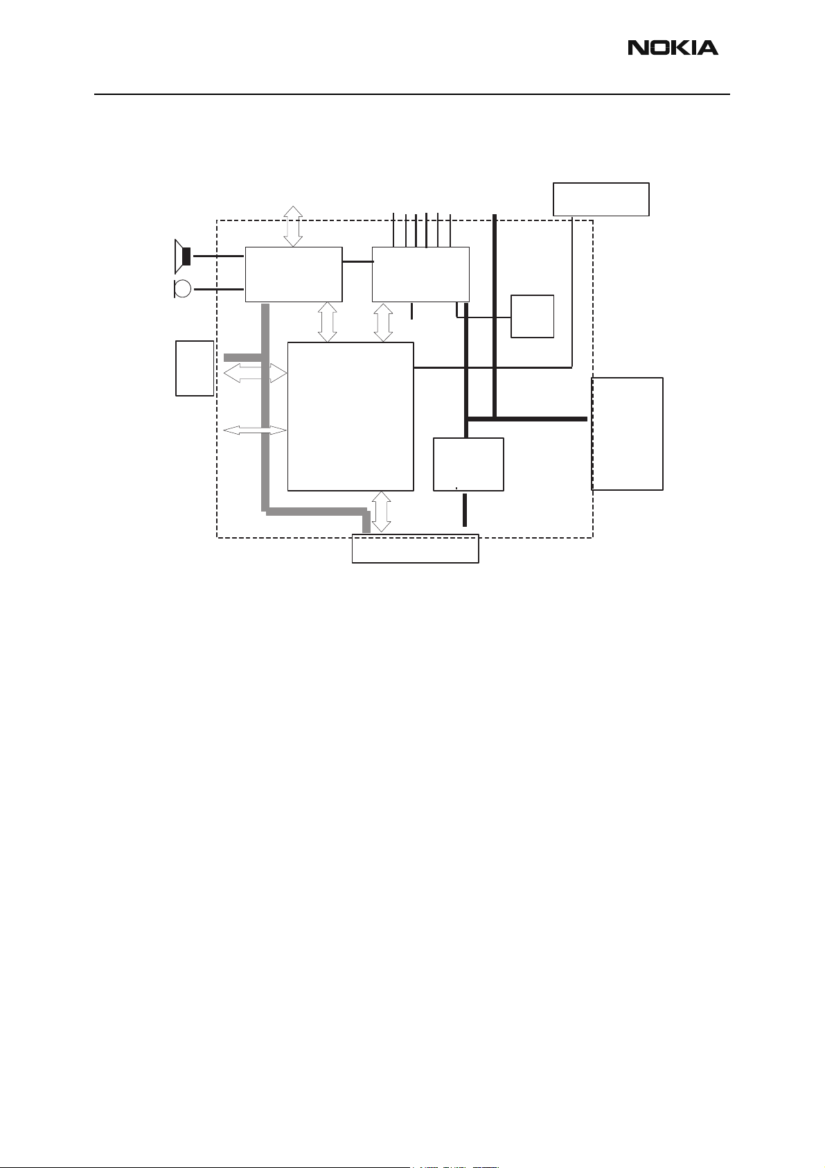
System Module
Circuit Description
The transceiver electronics consist of the Radio Module, RF + System blocks, the UI PCB,
the display module, and audio components. The keypad and the display module are connected to the Radio Module with connectors. System blocks and RF blocks are interconnected with PCB wiring. The Transceiver is connected to accessories via a bottom system
connector with charging and accessory control.
The RF block is designed for a handportable phone which operates in the CDMA 1900
system. The purpose of the RF block is to receive and de-modulate the radio frequency
signal from the base station and to transmit a modulated RF signal to the base station.
Connectors
System Connector
Figure 1: Bottom Connector
Note: Intelligent Battery Interface, IBI, is an accessory interface on the battery side of
the phone including the same signals as the bottom connector. The accessory (e.g., an IBI
accessory) can be a battery pack with special features or an accessory module attached
between the phone and a normal battery pack.
Issue 1 05/02 Nokia Corporation Page 9
Page 10
NSD-5
3. System Module PAMS Technical Documentation
Baseband Module and Interface
Block Diagram
TX/RX SIGNALS
Cafe SUPPLY
RF SUPPLIES
PA SUPPLY
SYSTEM CLOCK
19.2MHzCLK
UI
Baseband Elements
Baseband refers to all technology elements in the phone design, which do not include RF
functions. The Baseband Module therefore includes audio, logic control, signal processing, power supply, and user interface functions. Baseband functionality of this product
consists of third generation Digital Core Technology (DCT3) design solutions.
CCONT
BB SUPPLY
SYSCON
CHARGING
SWITCH
SLEEP CLOCK
BASEBAND
Cafe
MEMORIES
AUDIOLINES
MAD
+
Figure 2: Baseband Module and Interface Block Diagram
32kHz
CLK
VBAT
BATTERY
Baseband ASICS Description
MAD4
The MAD4 submodule includes the MAD4 ASIC (MCU, DSP, System Logic), external memories, and VIBRA circuitry.
The MCU block is used for general purpose processing applications such as UI control,
timers, PUP control, RX modem interface, audio control, evaluation of sensor data from
CCONT A\D, and battery charging control.
The DSP accommodates all communication protocols, such as CDMA data processing.
DSP also handles speech signal processing (e.g., vocodor).
The System Logic component includes: peripheral interface (MCU Parallel I/O, Serial I/O
[FBUS/MBUS]) and PWM control; accessory interface (FBUS); external memories interface; RF interface and control; clocking, timing, and interrupts; sleep control; CAFE control; user interface control; reset generator; clock generator; and test interface.
Page 10 Nokia Corporation Issue 1 05/02
Page 11

NSD-5
PAMS Technical Documentation 3. System Module
Baseband-related External Interface
For detailed information on interfaces to CCONT, CAFE, UI, and accessories, consult the
CCONT, CAFE, and accessory modules in this chapter.
FBUS
FBUS (Fast Bus) is a serial interface between the DSP and data accessories and between
the DSP and multipath analyzer. FBUS also is used as a data path during flash code
downloading. This interface is a full-duplex, asynchronous, two-line bus. Figure 3 illustrates the timing for the FBUS.
Figure 3: USART synchronous mode receive (flashing mode)
Parameter Definition Minimum Maximum Unit
Tsds Data setup to rising edge 90 110 ns
Tsdh Data hold from rising edge 90 110 ns
MBUS
MBUS is a serial data bus of MCU, which is used for flash downloading (clock), testing,
and communication with external devices. Supported baud rates are 9.6, 19.2, 38.4, and
57.6 kbit/s.
JTAG Interface
JTAG Interface is used for MAD4 ASIC emulation including DSP and MCU emulation.
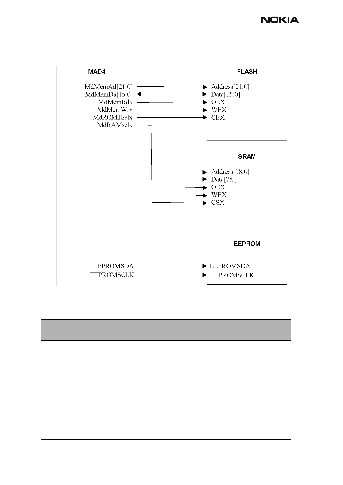
MAD4/External Memories Interface
Functional Description
The external memory consists of FLASH, SRAM, and EEPROM.
FLASH is used to contain the main program code for the MCU and EEPROM default values (local factory values). It has 2M x 16-bit size and uBGA package.
EEPROM stores tuning parameters and other systems permanently. Its size is 128k bytes.
The external memory interface is shared between the DSP and MCU processors. Both
8-bit and 16-bit external memories are supported. The interface supplies 22 address bits
to allow the MCU/DSP to address up to 4 Mbytes of linear address space for ROM1,
ROM2, and parallel EEPROM and 1 Mbyte of linear address space for SRAM (defined by
the chip-select signals). The DSP will use only the lower 16 bits of the address, and a
bank register is provided to set the 64K-word window for external memory accesses. A
read strobe, write strobe, and four-chip selects are provided for external memories.
Issue 1 05/02 Nokia Corporation Page 11
Page 12
NSD-5
3. System Module PAMS Technical Documentation
Table 1 illustrates the signal characteristics of the interface. Also see the MAD4 Technical Specification (Reference 1) for decoding memory map and chip selects.
Figure 4: Memory interface
Signal
MEMAD(21:0) < 0.62 > 2.24 MCU/DSP address bus to external memory
MEMDA(15:0) < 0.62 > 2.24 MCU/DSP bidirectional data bus to external
MEMRDX < 0.62 > 2.24 Read strobe to external memory
MEMWRX < 0.62 > 2.24 Write strobe to external memory
ROM1SELX < 0.62 > 2.24 FLASH chip select
ROM2SELX < 0.62 > 2.24 Not used
RAMSELX < 0.62 > 2.24 SRAM chip select
EEPROMSDA < 0.62 > 2.24 EEPROM serial data
Level (V)
Low High
Functional description
memory
Page 12 Nokia Corporation Issue 1 05/02
Page 13

NSD-5
PAMS Technical Documentation 3. System Module
Signal
EEPROMSCLK < 0.62 > 2.24 EEPROM serial data clock
Level (V)
Low High
Table 1: Electrical characteristics of the external memory interface
Functional description
Functional Timing Parameters
Memory access timing is treated asynchronously. There are two reasons for this type of
access. First, the external memories are inherently asynchronous. Second, two separate
processors running at different frequencies share the memories.
The following two figures (Figure 5 and Figure 6) provide timing information on MAD4
memory access. See MAD4 Technical Specifications (Reference 1) and DCT3 MAD4
Resource Manager Specification and Implementation (Reference 2) for additional timing
information on external memory read/write cycles.
Figure 5: External memory write cycle
Issue 1 05/02 Nokia Corporation Page 13
Page 14
NSD-5
3. System Module PAMS Technical Documentation
Figure 6: External memory read cycle
Parameters Flash memory SRAM
Min (ns) Max (ns) Min (ns) Max (ns)
Memory Write
Ts(addr) 70 80
Th(addr) 0 0
Ts(data) 60 40
Th(data) 0 0
Ts(ce) 70 80
Th(ce) 0 0
Tw(we) 70 70
Memory Read
Tcyc 110 100
Td(addr) 110 100
Td(oe) 30 50
Td(ce) 110 100
Table 2: Timing information for Read/Write cycle required/provided by memory chips
MAD4/VIBRA Interface
VIBRA is a vibrating motor, used as a silent alarm device. It is driven by 11kHz or 22kHz
PWM signal, with a variable duty cycle to control the average current into the motor,
which in turn controls the intensity of the alarm. The duty cycle is set by software and
depends on the motor and the limits of the duty cycle.
Page 14 Nokia Corporation Issue 1 05/02
Page 15

NSD-5
PAMS Technical Documentation 3. System Module
MAD4/RF Interface
MAD4/RF Synthesizer Interface
Functional Description
Figure 7 defines the MAD4/RF synthesizer interface. The synthesizer interface is capable
of programming National LMX2330L Dual PLL Frequency Synthesizer. See Figure 8 and
Reference 1 for synthesizer timing information such as set-up and hold time.
Signal Definitions
SYN_DAT
Figure 7: RF/MAD synthesizer interface
Figure 8: Synthesizer serial timing
Data sent from MAD pin E17 (mdRFSData) to the synthesizer divider and counters. It has
2.8V CMOS logic level.
High Low Reset/Inactive Current Filtering
Vdd - 0.6V 0 - 0.5V Low/low > 50 ns 1 mA max None
Issue 1 05/02 Nokia Corporation Page 15
Page 16

NSD-5
3. System Module PAMS Technical Documentation
SYN_CLK
19.2000 MHz clock sent from MAD pin E16 (mdRFSClk) to synthesizer. The rising edge of
the clock is used to clock data into the synthesizer.
High Low Reset/Inactive Current Filtering
Vdd - 0.6V 0 - 0.5V Low/low > 50 ns 1 mA max None
SYN_LE1
Loading enable signal from MAD pin F16 (mdRFSLE1) to RF for the dual synthesizer. See
data sheet of the synthesizer for details.
High Low Reset/Inactive Current Filtering
Vdd - 0.6V 0 - 0.5V Low/low > 50 ns 1 mA max None
AFC
Signal from MAD pin B17 (mdAFC) to RF VCTCXO to provide 19.2 MHz reference frequency adjustment. It is active in CDMA. When the level is above 1.2V, the frequency is
increased.
Type Range Resolution Current Filtering
PDM 0 - 2.8V 9bits @ 9.6MHz clock < 1 mA
BB: RC = 4.7 x 10
RF: RC = 1.0 x 10
-4
-5
Sec
Sec
Page 16 Nokia Corporation Issue 1 05/02
Page 17

NSD-5
PAMS Technical Documentation 3. System Module
MAD4/RF Receiver and Transmitter Interface
Figure 9: MAD/RF TX/RX interface
Functional Description
Figure 9 shows the interface between MAD4 and RF receiver and transmitter. It includes
transmitter enable/disable, and RF power controlling. Some of the control signals have
2.8 CMOS level, while others have a PDM signal, which can be used to control RF behavior. The MAD4 PDM output is 2.8 V CMOS digital signal with pulse duration modulated
with 9.6 MHz clock. Baseband provides low pass filter to smooth the signal and avoid
digital noise into RF ground plane.
Signal Definitions
TIF_EN
High Low Load impedance Polarity Rising Time Filtering
Vdd - 0.6V 0 - 0.5V Min: 20k
Typ: 200k
Low: Disable < 25 ns
(10% - 90%)
None
RF_TX_GATE_P
Signal from MAD4 pin B14 (RF_TX_GATE_P) to RF transmitter to activate the bias of cel-
Issue 1 05/02 Nokia Corporation Page 17
Page 18

NSD-5
3. System Module PAMS Technical Documentation
lular PA section and switch regulator providing cellular PA driver. PA is activated discontinuously in CDMA mode.
High Low Polarity Rising time Filtering
Vdd - 0.6V 0 - 0.5V High: TX on
Low: TX off
< 25 ns
(10% - 90%_)
BB: RC = 1.0 x 10
TX_LIM
Signal from RF transmitter to MAD4 pin E15 (rfTxLim) to indicate maximum allowed output power is being exceeded, therefore to dynamically adjust the maximum commanded
transmitter gain in CDMA mode.
High Low Polarity Rising time
Vdd - 0.6V 0 - 0.5V High: Power exceeded
Low: Power not exceeded
< 10 ns
TX_LIM_ADJ
Signal from MAD4 pin D16 (mdGPPDM2) to RF transmitter to set trig point of indicator
where maximum transmit power is exceeded in CDMA.
Type Range Resolution
PDM 0.3V - 2.8 V 8bits @ 9.6 MHz clock 1M
Load
impedance
-5
sec
Filtering
BB: RC = 1.0 x 10
-4
sec
TX_IF_AGC
Signal from MAD4 pin A15 (mdTxlfAgc) to IF VGA to control the gain of the transmit IF
section.
Type Range Resolution Filtering
PDM 0.3V - 2.8 V 9bits @ 9.6 MHz clock
BB: RC = 2.2 x 10
Signal from MAD4 pin C14 (mdTxIfAgc) to RF VGA to control the gain of the transmit RF
section. It tracks TX_IF_AGC signal with separate slope adjustment.
Type Range Resolution Filtering
PDM 0.3V - 2.5 V 8bits @ 9.6 MHz clock
BB: RC = 2.2 x 10
RIF_EN
Signal from MAD pin D2 (mdP1GPIO(2)) to RIF to enable RIF and to provide AGC reference with PDM high voltage.
-5
sec
-5
sec
Page 18 Nokia Corporation Issue 1 05/02
Page 19

NSD-5
PAMS Technical Documentation 3. System Module
RX_IF_AGC
Signal from MAD4 pin A16 (mdRxIfAgc) to RIF pin AGC to control the gain of the receive
IF section. It is activated only by CDMA.
Type Range Resolution
PDM 0 - 2.8V 8bits @ 9.6 MHz clock Min: 10k
Load
impedance
CAFE Module/Interface
CAFE Module Description
Introduction
CAFE module provides an interface between the digital portion of the phone (CDMA digital data and control signal processing) and the analog portion (RF). It consists of CAFE
ASIC and some discrete components around the ASIC. It also provides an interface
between MCU/DSP and external audio accessory.
Inside CAFE ASIC, there are several sub-blocks: CDMA receive A/D converter, CDMA
receive FIR filter, CDMA transmit D/A converter, PLL clock recovery circuitry, and audio
CODEC. Externally, the module contains some data buses and control lines, as well as
some clock signals.
Figure 10 provides a brief overview of the interface.
Filtering
BB: RC = 1.0 x 10
-4
sec
Issue 1 05/02 Nokia Corporation Page 19
Page 20

NSD-5
3. System Module PAMS Technical Documentation
.
Figure 10: CAFE module block diagram
Detailed Module Description
CDMA Mode
When the phone is in CDMA mode, I and Q components of the received IF signals from
RIF are differentially AC coupled to CAFE ASIC. The input signal levels, impedance, and
capacitance are described in Reference 3. For more information, refer to that document.
The received signals are A/D converted to 4-bit digital signals inside the CAFE ASIC and
then are sent to the MAD4 ASIC through data bus RXD[11:0]. The 4-bit in-phase compo-
Page 20 Nokia Corporation Issue 1 05/02
Page 21

NSD-5
PAMS Technical Documentation 3. System Module
nent, RXI, is RXD[11..8]. For load impedance and input/output rise/fall time and other
electric characteristics, refer to Reference 3 [CAFE application].
The transmitted signal is fed to the CAFE ASIC through data bus TXD[7:0] from MAD4
ASIC. The digital signal is registered inside CAFE ASIC. In-phase and quadrature components are separated from each other by using IQSEL from MAD4, and are D/A converted
to analog signals. The transmitted signals (I and Q components) are then converted to
differential signals and sent to TIF of RF section. The output signal levels are described in
the section “CDMA I and Q transmit channel D/A converters and post filters” of the CAFE
design specification (Reference 3). Signal CAFE_TX_GATE is used to control the power for
transmits DAC and filters inside the CAFE ASIC. When it is high, the power to those two
blocks is turned on; otherwise, the power is turned off.
Clock
A 19.2 MHz sine wave clock is sent from RF to CAFE ASIC. It is squared inside the CAFE to
provide 19.2 MHz square wave clock to MAD4. There is about 1.4V DC offset to the
19.2 MHz sine wave clock. It has to be DC-coupled to the CAFE ASIC. A phase-locked
loop is used to generate a 9.83 MHz signal. This clock also is sent to MAD4 and used as
CDMA system clock, which is eight times the chip clock (1.2288 MHz). The electric characteristics of the clock recovery circuit are described in the CAFE specification.
Audio
There are two kinds of audio inputs to the CAFE ASIC. The first is from the built-in microphone. The second is from an external accessory. The signal from the built-in microphone, MICP and MICN, is sent to CAFE differently, using pin F10 and pin E10. The
differential input signal range is from 200mVpp to 2.0Vpp, and depends on the gain setting inside the CAFE. (CAFE provides up to 20 dB gain.) The internal microphone is biased
by a DC signal from pin D11. It also could be biased by VR1_SW.
The audio signal from an external accessory part (XMICP/XMICN) is differentially sent to
CAFE through pin F11 and pin E11. The external microphone bias is provided by AUXOUT
at pin B11 when CODEC_XMIC_BIAS = 1 in control register 2.
The audio receive path consists of D/A converter, lowpass filter and output attenuator
with three selectable outputs. Only one output can be activated at a time. The bias at the
outputs can be independently controlled to be ON at all outputs to avoid switching transients. EAR output from pin A9 and pin B10 of CAFE ASIC is intended to drive the phone
earpiece having typical 32-ohm resistance in the audio band. Output is differential, with
positive (EARP) and negative (EARN) output terminals.
HF output is intended to drive the phone external audio circuitry (XEAR). Output is signal-ended, but it also has another pin (HFCM), which drives the signal ground for it.
External microphone input and external speaker output can be detected by signal HOOKINT, EAD, and EAD_HEADINT. For detailed information, consult the audio accessory specification (Reference 7).
Issue 1 05/02 Nokia Corporation Page 21
Page 22

NSD-5
3. System Module PAMS Technical Documentation
Figure 11: MAD/CAFE interface diagram
General Description
As shown in Figure 11, the interface between MAD4 and CAFE consists of a parallel
transmit bus (TxD), parallel receive bus (RxD) data, two serial data paths for both CAFE
control and CODEC audio transmit/receive data, and an 8 kHz frame sync for the serial
data bus.
The interface also includes the system clock and other required clocks. CAFE provides
MAD4 19.2 MHz system clock (CLK19M20) and the 9.8304 MHz CDMA clock (CLK9M83).
MAD4 creates internal clocks from the system clock. The 8 kHz sync signal is 320 kHz
period wide pulse (serial data interface rate). All data transmission and reception in the
MAD ASIC will be clocked in/out with the rising edge of the clocks and all data transmission and reception in CAFE will be clocked in/out with the falling edge of the clocks.
MAD4 also supplies CAFE with an active “low” power reset signal (mdResetX).
Signal Parameter Min Typical Max Function
CAFESIO(0)
“1” (V)
“0” (V)
T
SDOD
2.24
0
2.70
0.30
Vbb
0.62
20 ns
MAD to CAFE serial data for
CAFE control, and digitized rreceived audio data to CODEC
CAFESIO(1)
“1” (V)
“0” (V)
T
SD1H
T
SDISU
2.24
0
20 ns
20 ns
2.70
0.30
Vbb
0.62
CAFE to MAD serial data bus to
read CAFE control register data
and send digitized audio data to
MCD
Page 22 Nokia Corporation Issue 1 05/02
Page 23

NSD-5
PAMS Technical Documentation 3. System Module
Signal Parameter Min Typical Max Function
CAFESIO(2)
IQSEL
CAFE_TX_GATE
TXD(7:0)
RXD(11:0)
“1” (V)
“0” (V)
Tf (ns)
Tr (ns)
“1” (V)
“0” (V)
T
IQSU
“1” (V)
“0” (V)
T
TXGON
T
TXGOFF
T
TXGS
T
TXGH
“1” (V)
“0” (V)
T
(ns)
DH
T
(ns)
DSU
“1” (V)
“0” (V)
T
DRXD
(ns)
(ns)
(ns)
(ns)
2.24
0
TBD
TBD
2.24
0
20
2.24
0
10 us
10 us
10
10
2.24
0
20
20
2.24
0
2.70
0.30
2.70
0.30
2.70
0.30
2.70
0.30
2.70
0.30
Vbb
0.62
TBD
TBD
Vbb
0.62
8 kHz frame sync clock from
MAD to CAFE to synchronize
CAFE serial interface to MAD
I and Q selection from MAD to
CAFE. “1” is for I data and “O” is
from Q and AMPS data
Vbb
0.62
CAFE internal transmit enable
signal from MAD to CAFE (Active
“High”)
Vbb
0.62 8-bit parallel transmit data from
MAD to CAFE for both CDMA and
AMPS modes
Vbb
0.62
20
12-bit parallel receives data
from CAFE to MAD for both
CDMA and AMPS mode
“1” (V)
CLK19M20
“0” (V)
Tper (ns)
“1” (V)
CLK9M83
“0” (V)
Tper (ns)
“1” (V)
RESETX
“0” (V)
Tf (ns)
Tr (ns)
Tf:Falling time
Tr:Rising time
Delay time for data from CAFE to MAD4, from CLK19M20 to data valid
T
SDOD:
T
Hold time for serial data from MAD4 to CAFE
SDIH:
T
Setup time for serial data from MAD4 to CAFE
SDISU:
T
Setup time for IQSEL
IQSU:
T
T
T
T
T
T
T
T
TXGATE turn on time before first valid data
TXGON:
TXGOFF:
TXGS:
TXGH:
DH:
DSU:
DRXD:
per:
TXGATE turn off time after last valid data
Setup time for TXGATE
Hold time for TXGATE
Hold time for TXD(7:0)
Setup time for TXD(7:0)
Delay from CLK9M80 falling edge to valid RX data
Clock period
2.24
0
52.08
2.24
0
101.73
2.24
0
TBD
TBD
2.70
0.30
2.70
0.30
2.70
0.30
Table 3: MAD/CAFE interface signals
Vbb
0.62
52.08
Vbb
0.62
101.73
Vbb
0.62
TBD
TBD
19.2MHz system clock from CAFE
to MAD
9.8304MHz CDMA system clock
from CAFE to MAD
CAFE reset (active “low”) from
MAD to CAFE
Issue 1 05/02 Nokia Corporation Page 23
Page 24

NSD-5
3. System Module PAMS Technical Documentation
CAFE/MAD4 Serial Data Interface
MAD/CAFE serial data interface allows both DSP and MCU processors within MAD4 to
read/write CAFE control registers. It also provides a serial interface with MAD4 for the
CODEC to receive and transmit audio data.
The serial data is transferred at a 320KHz data rate. The frame structure for the serial
interface is based on an 8 kHz wide period where the control data is transferred in the
first half of the frame period and the audio data is transferred in the second half of the
frame period for both directions.
For details on the interface protocol, refer to the CAFE ASIC specification.
CAFE/MAD4 TX Interface
The MAD/CAFE TX interface consists of an 8-bit data bus output from MAD4 to CAFE to
be D/A converted to analog signal. The data transfer rate is 9.8304 MHz. The data to be
transmitted is clocked out of MAD4 at the rising edge of the 9.8304 MHz clock and
clocked into CAFE at the falling edge of the clock.
In CDMA mode, the data consists of alternating TXI and TXQ data. IQSel signal is used by
CAFE to select the appropriate I/Q component. When IQSel = ‘1’, the data is TXI component; when IQSel = ‘0’, the data is TXQ component.
For more information, see CAFE design specification.
TX Gate Enable
CAFE_TX_GATE is an active high-enable signal used to enable/disable CAFE internal TX
DACs. This signal is provided by the CDMA transmit block within MAD4 and is synchronized to the 9.8304MHz clock.
CAFE/MAD4 Clock/Reset Interface
The active low signal (RESETX) is used as an asynchronous reset for CAFE to set all internal registers to a known state when the system starts up.
CAFE provides MAD4 with two clocks. One is the system clock, which is 19.2MHz. The
other is a CDMA clock that is 9.8304MHz. MAD4 generates its internal lower rate clocks
for interface data transmission and reception. It also supplies an 8 kHz frame sync pulse
(CAFESIO2) to CAFE, which is used to create its own internal clocks for interface transmission and reception. These are synchronized to the equivalent clocks within the MAD
ASIC.
The following figure (Figure 12) shows the correlation and alignment of internal/external
clocks within these two ASICs.
Page 24 Nokia Corporation Issue 1 05/02
Page 25

NSD-5
PAMS Technical Documentation 3. System Module
CAFE/RF Interface
Figure 12: MAD/CAFE clock correlation/synchronization
Figure 13: RF/CAFE interface
General Description
As shown in Figure 13, the interface between the RF parts and CAFE has the following
signals (Table 4).
Issue 1 05/02 Nokia Corporation Page 25
Page 26

NSD-5
3. System Module PAMS Technical Documentation
Signal Parameter Min Typ Max Description
CLK19M22 Freq (MHz) 19.2 +/- 2.5 ppm 19.2MHz system clock input from
Phase
10Hz 100Hz 1000Hz
Noise (dBc/Hz)
-70 -110 -130
Settling Time 5ms
VCTCXO to clock squaring circuit
TX_IP Level (Vpp)
Noise (uVrms)
TX_IN
Level (Vpp)
Noise (uVrms)
TX_QP Level (Vpp)
Noise (uVrms)
TX_QN Level (Vpp)
Noise (uVrms)
RX_IP Level (mVpp)
Noise Figure (dB)
RX_IN Level (mVpp)
Noise Figure (dB)
RX_QP Level (mVpp)
Noise Figure (dB)
0.97 1.0 1.03
<450
0.97 1.0 1.03
<450
0.97 1.0 1.03
<450
0.97 1.0 1.03
<450
(1)
48
20 25
(1)
48
20 25
(1)
48
20 25
CDMA TX filter I channel differential output to TIF I/Q modulator
input
CDMA TX filter I channel differential output to TIF I/Q modulator
input
CDMA TX filter Q channel differential output to TIF I/Q modulator
input
CDMA TX filter Q channel differential output to TIF I/Q modulator
input
CDMA RX filter I channel input
from RIF I/Q demodulator output
CDMA RX filter I channel differential input from RIF I/Q demodulator
output
CDMA RX filter Q channel differential input from RIF I/Q demodulator
output
RX_QN Level (mVpp)
Noise Figure (dB)
48
(1)
20 25
CDMA RX filter Q channel differential input from RIF I/Q demodulator
output
(1) Center on Vref = 1.244V
Table 4: Electrical characteristics of the CAFE/RF interface signals
RX/CAFE CDMA RX Interface
The digital receive channel consists of two equal branches (RXI, RXQ). Each branch has
differential input and the signal is AC coupled. See Table 5 for details.
For I and Q channels Symbol Min Typ Max Unit
Passband frequency (-0.5 dB point) fpb 620 630 640 kHz
Stopband frequency fsb 900 kHz
Max differential input voltage
VI
pb
20 mVpp
range in passband
Page 26 Nokia Corporation Issue 1 05/02
Page 27

NSD-5
PAMS Technical Documentation 3. System Module
For I and Q channels Symbol Min Typ Max Unit
Max differential input voltage
range in stopband
Input impedance ZIN 10 13 16 kΩ
Table 5: RXI, RXQ receive channel characteristics
VI
sb
1Vpp
RF/CAFE CDMA TX Interfaces
The digital transmit channel consists of two equal branches (TXI, TXQ). Each branch has
differential output and the output signal is AC coupled. Table 6 lists some of the transmit
channel characteristics. For more information, consult the CAFE design specification
(Reference 3).
Symbol Parameter
Vout Output voltage Range (differential
to the load)
IM3 3rd order intermodulation distor-
tion
S/N Signal to noise ratio At passband 48 dB
Test
conditions
Centered on
Vref = 1.45V
Two tone test:
430 kHz,
600 kHz
Min Typ Max Unit
0.97 1.0 1.03 Vpp
-46 dB
ZL Load impedance 10 kΩ
CL Load capacitance 20 pF
HD Harmonic distortion -48 dB
Noise in 1.25 MHz - 10 MHz frequency band
F
-0.5dB
F
stop
A
stop
GD Group delay At passband 430 us
GDD Group delay distortion At passband 80 ns
GDM Group delay match between
Passband 630 kHz
Stop band 4.3 MHz
Stop band attenuation referred to
pass band gain
branches
Table 6: TXI, TXQ transmit channel characteristics
35 dB
10 ns
45 uVrms
Power Management (CCONT) Module and Interface
CCONT Module Functional Description
Power management and distribution is handled by the CCONT ASIC. CCONT is a multi-
Issue 1 05/02 Nokia Corporation Page 27
Page 28

NSD-5
3. System Module PAMS Technical Documentation
function power management ASIC which has seven 2.8V linear regulators for the RF section of the phone. One 2.8V regulator is used to power up the baseband of the phone.
Additionally, one adjustable regulator can be used to power up certain parts of the baseband. There also is a 5V charge pump, 5V regulator, and 3/5V regulator.
The main functions of CCONT are: voltage regulation, power up/down procedures, reset
logic, charging control (PWM), watchdog, sleep control, A/D conversion, and a real time
clock.
- Six user-controlled, 2.8V regulators
- Baseband regulator
- Programmable output voltage regulator for MAD core
- Voltage reference
- 32kHz oscillator and real-time clock
- +5V output
- 3V/5V switchable output
- Power-up control circuits, power-on reset
- Charger control circuits
- Charging switch and regulator
- 10-bit 8 input A/D converter (9 inputs with temp MUX)
- Serial bus control of all functions
- Alarm clock and charger interrupt
- Battery interface
CCONT Regulators
Battery voltage (VBAT) is connected to CCONT, regulating all the supply voltages (VBB,
VR1-VR7, VMAD, VR1_SW, VSIM, and V5V). CCONT default start-up mode turns on VR1,
VBB, VMAD, VR6, and Vref during power-up.
VMAD provides the MAD4 ASIC with a lower core voltage. VMAD is connected to those
pins on MAD4 that power the core.
During the sleep mode, most regulators are turned off except VBB and VR6 (when VBAT
is higher than 3.0V). During this period, VR6 is switched from VBB since VBB is supplying
power for VR6. For more information about RF power distribution, see Reference 5.
The maximum total output current from CCONT is 330mA (not including VR7). This is due
to thermal considerations at maximum battery voltage during charging. However, during
TX, when most outputs are enabled, the maximum current of each regulator can be
obtained. Software limits the average battery voltage to 3.8V (minimal charging).
Table 7 defines the regulator outputs of CCONT.
Output Control signal To
Noise level
(nVrms/℘Hz)
Max
current
(mA)
Range (Voltage)
Min Typ Max
VR1 CLK_EN OR
CtrlReg1(0)
Synthesizer 200 80 2.67 2.80 2.85
Page 28 Nokia Corporation Issue 1 05/02
Page 29

NSD-5
PAMS Technical Documentation 3. System Module
Output Control signal To
VR1_SW RFReg(2) XMIS bias
voltage
VR2 RFReg(1) Receiver 200 80 2.67 2.80 2.85
VR3 RFReg(0) Synthesizer 200 50 2.67 2.80 2.85
VR4 (CAFE_TX_GATE
AND BAND_SEL)
OR RFReg(3)
VR5 /BAND_SEL OR
RFReg(4)
VR6 RFReg(5) CAFE 200 80 2.67 2.80 2.85
VBB Always on Baseband 200 125 2.67 2.80 2.85
VREF CtrlReg1(1) CCONT, CAFE 30 uVrms 200 uA 1.244
VMAD CVReg MAD4 (Core,
Transceiver 200 80 2.67 2.80 2.85
TX power
detection
MCU, DSP)
Noise level
(nVrms/℘Hz)
200 10 2.67 2.80 2.85
200 80 2.67 2.80 2.85
(a)
N/S
Max
current
(mA)
50 1.30 1.75 2.65
Range (Voltage)
Min Typ Max
1.478
1.251
1.500
1.258
1.523
5V Serial data bus Transmitter
Vpp
_CCONT
(a) N/S: Not specified in data sheets.
(b) Maximum total current from all CCONT regulators is 330 mArms. The maximum current when both VR1 and
VR1_SW are used is 80 mA.
CtrlReg1(2) Flash memory
Table 7: CCONT regulator outputs
N/S
N/S
(a)
(a)
25 4.8 5.0 5.2
25 2.8
4.8
3.0
5.0
3.2
5.2
Watchdog
MAD4 must reset the CCONT watchdog regularly. CCONT watchdog time can be set
through SIO between 0 and 63 seconds at 1 second steps. After power–up the default
value is 32 seconds. If the watchdog expires, CCONT will cut off all supply voltages. After
total cut–off the phone can be re–started through any normal power–up procedure.
CCONTs watchdog functionality may be temporarily disabled by holding CCONTs
PWRONX/WDDISX pin at logic low.
Power Up
There are four ways to power on the phone.
1. Power Up by Power Button
2. Power Up With Charger Connected
3. Power Up by IBI
Issue 1 05/02 Nokia Corporation Page 29
Page 30

NSD-5
3. System Module PAMS Technical Documentation
4. Power Up With RTC
Each of four methods is described in general in the following sections. When the battery
is connected to phone, nothing will happen until the power–up procedure is initiated; for
instance, by pressing the power button or by connecting a charger. After that the 32kHz
crystal oscillator of CCONT is started (can take up to 1 sec), and the default regulators
are powered up.
If a power down is done and the battery remains connected, the 32 kHz crystal oscillator
keeps running in the CCONT.
Figure 14: Power Distribution Diagram
Page 30 Nokia Corporation Issue 1 05/02
Page 31

NSD-5
PAMS Technical Documentation 3. System Module
Power Up by Power Button
t1< 1 ms
t211 - 6 ms, VCXO settled
t
: 62 ms, PURX delay generated by CCONT
3
(*)VR1 VR6 and Vref might be later than VBB
Figure 15: Timing of power-up sequence by power button
After PWR–key has been pushed, CCONT sends PURX reset to MAD4 and turns on VR1,
VBB, and VR6 regulators (if battery voltage has exceeded 3.0 V). VR1 supplies VCTCXO,
VBB supplies MAD, and VR6 supplies CAFE. After the initial delay, t2, VCTCXO starts to
give a proper 19.2MHz clock to CAFE, which further divides it to 9.83MHz for MAD4.
CAFE will output the 9.83MHz clock only after the PURX reset has been removed. After
delay, t3, CCONT releases PURX and MAD4 can take control of the operation of the
phone.
After MAD4s reset is released, MCU–SW detects that the PWR–key is still pushed and
shows the user that the phone is powering up by turning on the LCD and the lights.
MCU–SW then powers up the RF receiver part. See Figure 16 for timing information.
Issue 1 05/02 Nokia Corporation Page 31
Page 32

NSD-5
3. System Module PAMS Technical Documentation
Power Up When Charger Connected
Figure 16: Timing of power-up sequency by a charger
The power-up procedure is similar to the process described in the previous section, with
the exception that the rising edge of VCHAR triggers the power up in CCONT.
CCONT sets output CCONT_INT, MAD4 detects the interrupt and reads CCONT status register to find the reason for the interrupt (charger in this case). After reading the A/D register to determine that the charger voltage is correct, MAD should initiate charging
activities. The phone will remain in the so-called ”acting dead” state, which means that
only the battery bars are displayed on the LCD. The user perceives that the phone is off. If
the power-on button is pushed, the LCD display will come on and startup will be the
same as normal power on.
CCONT_INT is generated both when the charger is connected, and when the charger is
disconnected. It goes high when a valid charger is connected or the alarm clock times
out (real time clock). Once high, the MAD must actively reset this via the serial port. If
two interrupts occur at the same time, the interrupt line will not go high until all interrupts have been cleared.
If the battery is empty (lower than 3.0V), CHAPS gives an initial charge (with limited current) to the battery before the battery voltage rises above 3.0V. After the battery voltage
reaches 3.0V, the power-up procedure described in the previous section takes place. See
Figure 16 for timing information.
Page 32 Nokia Corporation Issue 1 05/02
Page 33

NSD-5
PAMS Technical Documentation 3. System Module
Power Up by IBI
IBI can power CCONT up by setting BTEMP to logical “1”. The recommended pulse width
of the pulse is longer than 10 msec. After that, BTEMP acts as normal A/D input. Otherwise, the power-up procedure is the same as with the charger.
Power Up With RTC
RTC can power up the phone by setting the CCONT internal signal RTCPwr to logical “1”
Otherwise, the power-up procedure is the same as with the charger.
Charging – CHAPS
CHAPS comprises the hardware for charging the battery and protecting the phone from
over–voltage in charger connector. CHAPS operates in temperature ranges from -30o to
130o C. The software can stop charging based on the battery temperature to protect the
battery from being damaged (e.g., the cutoff temperature for the nickel battery is 47o C;
the cutoff temperature for the lithium battery is 85o C). Figure 17 gives a brief block dia-
gram of the charging submodule.
The main functions of CHAPS are:
• protection against transient, over–voltage, and reverse charger voltage
• limited start–up charge current for a totally empty battery
• limit voltage when battery removed
• software protection against overcharging current
CHAPS is basically a PWM (Pulse Width Modulation) controlled switch, which connects
the charger to VBAT. MAD4 controls CHAPS by writing PWM values to CCONT PWM register over a serial bus. CCONT then outputs a PWM, which is used by CHAPS to control
the switch. In the case of an external fast charger, the PWM is not available at the system connector to control the charger. There are only two wires connected to the
charger. In the case of a dead battery, shorted battery, or a battery below 3.0V, CHAPS
supplies a controlled leakage current of about 180mA through the switch to attempt to
bring the battery voltage up.
Figure 17: Charging block
Issue 1 05/02 Nokia Corporation Page 33
Page 34

NSD-5
3. System Module PAMS Technical Documentation
With 2–wire charging, the charger provides constant output current, and the charging is
controlled by the PWMOUT signal from CCONT to CHAPS. PWMOUT signal frequency is
1 Hz, and the charging switch in CHAPS is pulsed on and off at this frequency. The pulse
width of PWMOUT is controlled through the serial data bus.
There is a protection mechanism in CHAPS to protect the phone from over-charging the
phone’s voltage. When a charger is connected to the phone, if VBAT exceeds preset limits
in CHAPS, the switch immediately turns OFF (soft switching is bypassed). There are two
voltage limits: VLIM1 and VLIM2. VLIM input = “0” selects VLIM1; VLIM input = “1”
selects VLIM2.
Symbol Parameter Min Typ Max
VLIM1 (V) Output voltage cutoff limit (during transmission or Li-battery) 4.4 4.6 4.8
VLIM2 (V) Output voltage cutoff limit (no transmission or Ni-battery) 4.8 5.0 5.2
When the switch turns off due to an overvoltage condition, it stays off until the input
voltage falls below the specified limit (VCH<VBAT). Phone software will stop the charging as fast as it detects that there is no battery present.
CCONT/MAD4 and CCONT/Others Interface Signals
Table 8 lists all of the inputs and outputs of the Power Management section.
Signal To
CLK_EN CCONT > 2.4 < 0.62 16 ns 16 ns Enable VR1 and CAFE
CCONTCSX CCONT > 2.4 < 0.62 16 ns 16 ns Serial bus select
UIF_CCONT_SDIO CCONT > 2.4 < 0.62 10 10 Serial bus data
UIF_CCONT_SCLK CCONT > 2.4 < 0.62 10 10 Serial interface clock, also
CCONT_INT MAD > 2.1 < 0.5 25 25 Interrupt signal to MAD
PURX MAD > 2.1 < 0.5 25 25 Power up reset
SLEEPCLK MAD > 2.1 < 0.5 25 25 32 kHz clock
VLIM CHAPS > 2.24 < 0.62
Signal Level (V)
High Low
MAD4
Rising
time
(a)
N/S
Falling
time
(a)
N/S
Function
CDMA clock output
used for LCD
Chaarge voltage limit
control
CAFE_TX_GATE from MAD > 2.24 < 0.62 16 ns 16 ns
RF
PA_TEMP from TX
N/A
(b)
N/A
(b)
N/A
(b)
N/A
(b)
PA temperature mux’ed
with VCXO_TEMP
Page 34 Nokia Corporation Issue 1 05/02
Page 35

NSD-5
PAMS Technical Documentation 3. System Module
Signal To
Signal Level (V)
High Low
MAD4
Regulator Outputs
Battery
VBAT from battery VBAT VBAT
BSI from battery
BTEMP from battery
N/A
N/A
(b)
(b)
N/A
N/A
CAFE
EAD_HEADINT from CAFE
SGND
N/A
N/A
(b)
(b)
N/A
N/A
OTHERS
PWRONX > 2.1 < 0.5
(b)
(b)
(b)
(b)
Rising
time
(b)
N/A
(b)
N/A
(b)
N/A
(b)
N/A
(b)
N/A
(b)
N/A
(c)
N/A
Falling
time
(b)
N/A
(b)
N/A
(b)
N/A
(b)
N/A
(b)
N/A
(b)
N/A
(c)
N/A
Function
See CCONT regulators for
details
Battery input
Battery type
Battery temperature,
muxed with VIBRA
External
accessory interrupt
Audio ground
Power on,
watchdog disable
V_IN from charger V_IN V_IN
L_GND from charger 0 0
CHRG_CTRL CHAPS > 2.1 < 0.5
(a) N/S (not specified in the data sheets)
(b) Analog signals. The level depends on input. No rising/falling time.
(c) Depends on switched speed.
N/A
N/A
N/A
Table 8: Power Management Inputs/Outputs
(b)
(b)
(a)
N/A
N/A
N/A
(b)
Charger input
(b)
Charger ground
(a)
PWM control signal
Issue 1 05/02 Nokia Corporation Page 35
Page 36

NSD-5
3. System Module PAMS Technical Documentation
User Interface
Functional Description
As shown in Figure 18, the MAD4 serial interface is used to control the serial LCD on the
user interface (UI) board and also to provide access to CCONT’s registers. The DataSelX
and DataClk are generated by MAD4 during both transmit and receive cycles. Each device
has its own chip select signal and must hold its data pin in a high-impedance state if its
chip select is not active. Data must be valid on the rising edge of DataClk during both the
transmit and receive cycles.
Figure 18: UI system interface block diagram
The LCD driver requires 9-bit data from the MAD UIF block. The MSB indicates whether
the following 8-bit is data or command. When this bit is high, the following 8-bits are
display data; otherwise, when it is low, the following 8 bits are control data.
The chip enable line also has to be modified to accommodate the interface. The new /CE
is from one of the GPIO pins (port 1, bit5).
The user interface also monitors the PWR key and keyboard, as well as controlling the
LCD, backlight, microphone, earpiece, and alert (buzzer, VIBRA, LED).
Signal Definitions
Table 9 defines the electrical characteristics of the user interface signals. For details on
the interface signals, refer to the design specifications for MAD4 and UI.
Signal To
COL(4:0) Keypad > 2.24 < 0.62
ROW(5:0) Keypad > 2.24 < 0.62
Signal Level (V)
High Low
Rising
time
(a)
NA
(a)
NA
Falling
time
(a)
NA
(a)
NA
Function
drives the keyboard
colums
sample keyboard rows
and drives the LCD
interface
LCD-CS LCD > 2.24 < 0.62 10 ns 10 ns chip select for the
LCD
Page 36 Nokia Corporation Issue 1 05/02
Page 37

NSD-5
PAMS Technical Documentation 3. System Module
Signal To
UIF_CCONT_SCLK LCD/CCONT > 2.24 < 0.62 10 ns 10 ns serial port clock
UIF_CCONT_SDIO LCD/CCONT > 2.24 < 0.62 10 ns 10 ns serial data
CCONTCSX CCONT > 2.24 < 0.62 16 ns 16 ns chip-select to the
(a) RC filters with time constant = 100 ns used on these signals for ESD protection.
Table 9: Electrical characteristics of the user interface
Signal Level (V)
High Low
Rising
time
Falling
time
Function
CCONT serial device
Functional Timing
Serial Port Functional Timing
Figures (19) and (20) provide LCD serial interface timing information. Reference 1 gives a
detailed description of the functional timing requirements for the serial port interface.
See Reference 6 for a detailed description and timing of the serial protocol for the
CCONT device. See Reference 1 for a detailed description and timing of the serial protocol for the serial LCD device.
Figure 19: Serial port transmit timing
Figure 20: Serial port receive timing
Parameters Definition Minimum Maximum Unit
Tcspd Falling edge to chip select 100 ns
Tcdpd Falling edge to command/data select 100 ns
Tsdo Falling edge to data out 0 ns
Issue 1 05/02 Nokia Corporation Page 37
Page 38

NSD-5
3. System Module PAMS Technical Documentation
Parameters Definition Minimum Maximum Unit
Tsdis Data in setup to rising edge 10 ns
Tsdih Data in hold from rising edge 10 ns
Table 10: Serial port timing
System/Accessory Interface
Description
External accessory interface specifies a connector and set of signals that allow the phone
to be used with a variety of standard peripherals (See Figure 21 following).
XEAR, XMICP, XMICN, EAD_HEADINT, and SGND are used to connect hands-free, headset,
and other accessories that require analog audio signal connections.
The VIN is used for battery charging.
Figure 21: External accessory interface
Signal Definitions
The interface signals include XEAR, XMICP, XMICN, EAD_HEADINT, SGND, L_GND, and
VIN. The function of these signals are defined as follows:
XEAR Audio output signal to the external speaker on the HFU or headset
SGND Audio output return (ground) path
XMICP External microphone input
XMICN External microphone input return (ground) path
EAD_HEADINT External audio accessory interrupt input to MAD4
Page 38 Nokia Corporation Issue 1 05/02
Page 39

NSD-5
PAMS Technical Documentation 3. System Module
VIN Charging input
L_GND Charging ground
IR Interface
If the phone supports internal infrared connection, the phone is set manually to infrared
mode, via the user interface SW selection. This is the only way to configure the phone for
the infrared mode. The infrared connection is always a point-to-point connection.
Once the infrared mode is selected, the phone begins to operate via the infrared connection using the IrDA protocol.
The disconnection of the infrared mode also is a manual operation involving the user
interface SW selection. If another accessory using cable is connected to the phone when
the phone is in infrared mode, that accessory is disregarded until the phone has been
disconnected from the infrared mode.
Audio Accessories
There are two types of audio accessories: headset and plug-and-play hands-free car kit.
XIMCP, XMICN, XEAR, and SGND are signals used for the external audio accessories.
XMICP and XMICN provide the differential input from the external microphone to the
CAFE. XEAR signals ended audio output to the external speaker. SGND is the ground for
the external speaker.
The headset accessory is simple to use. It consists of only an earpiece, a microphone, and
a HOOK-switch button, which can be used to answer a call or to end a call. The level of
signal HOOKINT can detect the status of the HOOK. When the button is pushed, a negative pulse is generated at HOOKINT to inform MCU that there is an interrupt from external audio accessory to initiate or terminate a call.
The plug-and-play hands-free car kit is an active audio accessory that contains an integrated loudspeaker and an option to connect an external microphone (unless the phone’s
built-in microphone is used).
The HF_MUTE signal is used to mute the external HF speaker.
A balanced configuration is used for the headset, which is accomplished by using two
1 kOhm for biasing the microphone.
When a headset is connected to the phone, EAD_HEADINT is pulled up since the spring
contact on the jag is open. MCU then checks the level on the EAD line through the
CCONT to determine which kinds of accessories are connected.
When a plug-and-play hands-free unit is connected, the voltage EAD is higher since
there is no microphone inside the plug-and-play and the plug-and-play provides approximately 2.1 to 2.7 Vdc voltage to the XMICP. Depending on the status of the external
microphone for the plug-and-play, the MCU determines whether to use the built-in
Issue 1 05/02 Nokia Corporation Page 39
Page 40

NSD-5
3. System Module PAMS Technical Documentation
microphone or the external microphone.
When the PPH1 is used, the MCU software ignores the interrupt from HOOKINT since the
PPH1 uses the TALK key on the phone to answer/end a call.
Table 11 describes the detection for the audio accessories. For more detailed information,
refer to Reference 7.
AUXOUT = “1.5 V”
HF_MUTE = “L”
No accessory
LPS - 3 H H 431 - 742 Un - mute
JBA - 6 H H 395 - 485 Un - mute
HS (button open) H H 431 - 742 N/A
HS (button close) H L 290 - 362 N/A
PPH (built-in mic) Charging On
Charging OffHH
PPH (exter mic) Charging On
Charging OffHH
PPH without power H L or H 353 - 440 N/A
Note:(1) L (logic low) is 0 - 0.5V and H (logic high) is Vdd - 0.6V
(2) This value will change, depending on charging and PCB layout because of the grounding between charger and
audio accessory. WhenPPH-1 is used, the charger should be connected and on.
EAD_HEADINT HOOKINT EAD (mV)
(1)
L
Table 11: External audio accessory detection
H< 100N/A
L or H
L or H
L or H
L or H
110 2 - 1 261
110 2 - 1 261
915 - 1067
915 - 1067
(2)
(2)
P&PHF
Speaker Muter
Un - mute
Un - mute
Un - mute
Un - mute
Battery Interface
Signal Characteristics
In addition to VBAT output and the ground, the battery has two additional outputs:
BTEMP and BSI. BTEMP is used to indicate the battery temperature and BSI is used to
indicate the battery type. BTEMP also is used as an input of VIBRA pulse width modulated signal for a battery with a built-in VIBRA. The Janette battery interface provides
detailed descriptions of these signals. For more information refer to this document.
BSI and BTEMP Connections
BTEMP Connections
A pull-up resistor to Vref is located on the phone side on the BETMP line. NTC pull-down
resistor is used in nickel batteries to give battery temperature information to the phone.
This is used by charging algorithm to change charging mode or terminate charging if the
battery temperature gets too high. The voltage level from this resistor divider is connected to CCONT A/D input. See Figure 22 block diagram of the interface.
Page 40 Nokia Corporation Issue 1 05/02
Page 41

NSD-5
PAMS Technical Documentation 3. System Module
Figure 22: The interface between battery and transceiver (|)
BTEMP Connections, IBI Accessories
All accessories that can be connected between the transceiver and the battery or that
itself contain the battery are called IBI accessories.
Either the phone or the IBI accessory can turn the other on, but both possibilities are not
allowed in the same accessory.
IBI accessory can power on the phone by pulling the BTEMP line up to 3V for at least
10ms.
BSI Connections
There is a pull-up resistor to VREF on the BSI line. A pull-down resistor is used in the battery pack (See Figure 23). Different pull-down resistance is used to indicate different
battery types. The voltage level from this resistor divider is connected to CCONT BSI A/D
converter input. The following items can be detected by using a different resistor in the
battery pack: lithium battery voltage and dummy battery (used for testing).
Issue 1 05/02 Nokia Corporation Page 41
Page 42

NSD-5
3. System Module PAMS Technical Documentation
Figure 23: The interface between battery and transceiver (||)
RF Module Overview
The RF Module is compliant with the requirements of J-STD-018. Constructed on a sixlayer PCB that is 1.0mm thick, the dielectric separating the layers is RCCu. All other
dielectrics measure FR4.
Environmental Specifications
The ambient temperature range is from -30oC to +85oC.
Vibration and Free Fall
Specifications are listed in the NMP Standard Product Requirements.
Humidity and Water Resistance
Specifications are listed in the NMP Standard Product Requirements.
Technical Specifications
Block diagram of the RF section, including the 1900MHz transmitter and receiver and
the synthesizer.
TX frequency: 1850MHz - 1910MHz
RX frequency: 1930MHz - 1990MHz
TX IF frequency: 208.1MHz
RX IF frequency: 128.1MHz
Page 42 Nokia Corporation Issue 1 05/02
Page 43

NSD-5
PAMS Technical Documentation 3. System Module
Maximum Ratings
The maximum battery voltage during the transmission should not exceed 4.5V. Higher
battery voltages may destroy the power amplifier and other circuitry. The minimum battery voltage is 3.2V.
RF Connector
If nothing is plugged into the phone, the RF is connected to the single band antenna.
When the RF connection is made, the RF path is switched mechanically from the antenna
to the cable plugged in. Note: the RF connector is designed for RF tuning in the factory;
it is fragile and could be pulled off easily, destroying the PWB if care is not taken.
Single Band Internal Antenna
A single band 1900MHz internal antenna has been developed for the U.S. PCS band.
Antenna gain is 2-3dBi across the band. The transmitter output power is tuned to
23.2dBm to 23.5dBm at the RF connector.
Transmitter
The following sections describe the PCS transmitters working from the baseband signals
to the duplexers.
Duplexer
The front of the duplexer is covered with a shield. It is crucial that this shield is well soldered down to avoid rejection problems. Solder joints along the mono block front (i.e.,
shield side) also are critical for rejection, while solder joints at the rear of the duplexer
serve only for mechanical securing. Due to the problem of silver leaching, the corners of
the duplexer should NOT be soldered. Only flat sections of the part should be soldered.
Parameter Transmitter Port Receiver Port
Insertion loss 3.3dB 3.7dB
Ripple (slope) 2.7dB 2.7dB
1850 - 1910MHz rejection 48dB
1930- 1990MHz rejection 44dB
Table 12: Typical performance of the Scorpion duplexer
Power Amplifiers Module 1900MHz
The power amplifier is a GaAs HBT device. The PCS PA is reference designator N604. This
is a two-stage device with interstage matching; it does not require an external output or
input match. It is packaged in a standard module plastic package with a heat sink slug
underneath. The metal slug on the underside, which serves primarily as a heat sink, also
serves as a RF ground connection. A grid of vias is present under the slug to help conduct
heat into the PCB. All layers have a maximum amount of copper under the PAs to assist
with heat dissipation.
The PA is connected directly to Vbatt. The PA is switched on and off by controlling its
Issue 1 05/02 Nokia Corporation Page 43
Page 44

NSD-5
3. System Module PAMS Technical Documentation
bias. Since a voltage of greater than 3.8V was required for the bias, the 5-volt output
from CCONT has been utilized. The collectors of both stages of the PA are based from the
battery source. The reference current provided by the current source (formed by V601
and V602) controls gain of PA module by means of the Iref pin. The Tx-Gate signal is used
to switch a current mirror to switch the PA with approximately 4 mA current. If there is
no RF input to the PA, then it will draw approximately 100mA.
1900MHz PA
Gain 25dB
Table 13: Typical gain of the PA
1900MHz Transmitter Interstage Filtering
Due to the small separation between the U.S. PCS Tx Band (1930 - 1990MHz) and the Rx
band (1850 - 1910MHz), it is extremely difficult to filter the Tx noise from the Rx band
to a level acceptable to the receiver. The split band filter provides the Rx band rejection.
A single SAW filter cannot provide the rejection due to the wide PCS band and the small
separation between the Tx and Rx in PCS band. The split band filter output is connected
to a SPDT RF switch.
1900MHz Upconverter
The 1900MHz upconverter has been designed with discrete circuitry for PWB space reasons and yield issues with the original MA/COM upconverter used in DCT3 (Apache).
A discrete solution has been designed with the IFA, mixer, RFA, and VVA in the same configuration as in the Apache IC. The VVA used is AT119. The gain distribution between the
IFA and RFA has changed from DCT3. A discrete mixer CMY211 is used for upconversion
and it has a much better IIP3 as compared to the mixer inside Apache IC. This allows IFA
gain to be increased and RFA gain to be decreased, which will dramatically improve the
Tx SNR (signal-to-noise ratio) at low powers. This results in far better low power Rho as
compared to DCT3.
The ACPR over the entire range of Tx power is also better than DCT3. Current consumption of the entire upconverter is around 35mA. The discrete upconverter consists of V604
(IFA), N605 (mixer), and V605 (RFA).
Driver
The PCS driver used is a single-input, double-output amplifier. The outputs can be
selected through a digital control (CH). All inputs and outputs are single-ended, 50 ohm,
and matched. This amplifier is used in the Tx chain to increase the power of CDMA signals to the PA module. It consumes a low amount of current.
Transmitter Intermediate Frequency (TIF)
The TIF IC generates the intermediate frequency (IF) for the 1900MHz transmitter. This IC
reference designator (N604) incorporates the IQ modulator for CDMA mode, 85dB of
dynamic range control, and a switch for the two transmitters. Also included in the TIF IC
is most of the circuitry required for the power detection for CDMA over power detection
Page 44 Nokia Corporation Issue 1 05/02
Page 45

NSD-5
PAMS Technical Documentation 3. System Module
.
Receiver
The following sections describe the Rx section chain from duplexer down to the I/Q signals for CDMA fed to the baseband.
Front End
In DCT3, the Stealth LNA and downconverter was used with an external bipolar LNA. In
Zim, the Alfred front end (N701) is used (same as that of Columbia). The 800MHz section
of Alfred IC is unused. It is critical that the LO must be present 5ms before Alfred is powered on. The software has been informed about this. This is a very linear part. Alfred is a
trimode dualband receiver front end (with 800MHz section not used). It houses LNAs and
downconverters (a combination of RFA, passive mixer, and IFA) for each band. The internal LO buffer provides the necessary gain to the UHF Rx LO to the level the mixer wants
to see. The mixer output feeds the IF filter single-ended. The LNAs have single-ended
inputs and outputs. External matching components are provided for both the LNA and
the mixer. The LNA is bypassable.
Mode NF
high gain 12dB 1.5dB 7dBm 5mA
LNA bypass -5dB 4dB 20dBm 0.1mA
IIP
3
Current
Table 14: PCS 1900MHz LNA Specs
Issue 1 05/02 Nokia Corporation Page 45
Page 46

NSD-5
3. System Module PAMS Technical Documentation
Min LO drive -7dBm
Max LO drive -3dBm
Gain =16dB
NF =4dB
IIP
3
Current =13mA
Interstage SAW Filter
The Rx interstage filter used is Z702. Insertion loss = 4.1dB.
Attenuation
DC - 1700MHz = 20dB
1850MHz - 1910MHz = 15dB
2058MHz - 2118MHz = 15dB
2186MHz - 2246MHz = 22dB
2246MHz - 6000MHz = 10dB
IF SAW Filter
2dBm
Table 15: PCS 1900MHz Downconverter Specs
The IF SAW filter used is Z703.
Key Parameters
Center frequency 128.1MHz
Insertion loss 6dB to 10dB
3dB pass bandwidth +/- 615KHz
Attenuation +/- 1.25MHz 37dB
Receiver Intermediate Frequency (RIF)
The RIF IC incorporates the following functions: CDMA AGC, IQ Demodulator. These functions are explained in the sections that follow. The RIF IC is powered from the VR3 regulator from CCONT and consumes approximately 24mA of current. The RIF IC reference
designator (N730) is packaged in an LFBGA 36.
Page 46 Nokia Corporation Issue 1 05/02
Page 47

NSD-5
PAMS Technical Documentation 3. System Module
CDMA AGC
The RIF IC contains a wide dynamic range AGC circuit for CDMA. The AGC provides +42.5
to -42.5dB of gain controlled by the PDM line RX_IF_AGC.
IQ Demodulator
The IQ demodulator mixes the 128.1MHz IF signal down to DC with two mixers, one at
quadrature to the other. The LO is at 256.2MHz and is divided by two in the demodulator.
Synthesizer
The synthesizer module supplies local oscillator signals for up/down conversion, channel
selection, AFC control, and system clock requirements. Devices are manufactured by
Fujitsu and National Semiconductor. The dual synthesizer is LMX2330L; the single synthesizer is MB15C130. The four submodules include:
1st Rx/2nd Tx UHF LO Synthesizer
This submodule contains a UHF VCO, a loop filter, and the RF half a dual synthesizer IC.
The function of this section is Tx/Rx channel selection. The step size is dependent on the
channel spacing of the band to be tuned. In the Rx path, the LO drives the down-converter. In the Tx path, the LO drives the up-converter. Dual-buffered output VCOs are
being used.
1st Tx VHF LO Synthesizer
This submodule contains a VHF VCO, a loop filter, and the IF half of a dual synthesizer.
This synthesizer is only tuned to a single frequency. The LO converts baseband data at
the input of the I/Q modulator to the 1st IF. The lock detect signal is filtered and sent to
Issue 1 05/02 Nokia Corporation Page 47
Page 48

NSD-5
3. System Module PAMS Technical Documentation
the baseband for Tx out-of-lock detection.
2nd Rx VHF LO Synthesizer
This submodule contains a VHF VCO, a loop filter, and a single synthesizer. This synthesizer is only tuned to a single frequency. The LO converts the received signal to baseband
data. This submodule will use a mask programmable synthesizer (Fujitsu).
System Reference Oscillator (VCTCXO)
This submodule is the reference clock for the engine. It is a voltage-controlled temperature compensated crystal oscillator that can be pulled over some range of its output frequency. This allows for an AFC function to be implemented for any frequency accuracy
requirements. The oscillator is temperature compensated to maintain tight center frequency control. Closed loop AFC operation will allow very close frequency tracking of the
base station to be done in PCS mode. This will enable the unit to track out aging effects
and give the required center frequency accuracy for CDMA in PCS bands.
Figure 24: The block diagram of synthesizer
Page 48 Nokia Corporation Issue 1 05/02
Page 49

NSD-5
PAMS Technical Documentation 3. System Module
Figure 25: Block diagram of basic phase locked loop
The LMX2330L of monolithic, integrated, dual frequency synthesizers, including prescalers, is to be used as a local oscillator for RF and first IF of a dual conversion transceiver.
In this explanation of LMX2330L IC, RF means the frequency range of the TX/RX UHF and
IF is the frequency range of the TX-VHF.
The LMX2330L contains dual modulus prescalers. A 64/65 can be selected for the RF synthesizer and a 8/9 prescaler can be selected for the IF synthesizer. LMX2330L, which
employs a digital phase locked loop technique, combined with a high-quality reference
oscillator, provides the tuning voltages for voltage-controlled oscillators to generate very
stable low noise signals for RF and IF local oscillators. Serial data is transferred into the
LMX2330L via a three-wire interface (data, enable, clock).
Functional Description of LMX2330L
Two 15-bit R counters and the 15- and 18-bit N counters. The data stream is clocked (on
the rising edge of clock) into the DATA register, MSB first. The data stored in the shift
register is loaded into one of four appropriate latches on the rising edge of LE. The last
two bits are the control bits. The DATA is transferred into the counters as follows:
Programmable Reference Dividers (IF and RF R Counters)
If the control bits are 00 or 01 (00 for IF and 01 for RF), data is transferred from the
22 bit shift register into a latch, which sets the 15-bit R counter. Serial data format is
shown here:
Issue 1 05/02 Nokia Corporation Page 49
Page 50

NSD-5
3. System Module PAMS Technical Documentation
Control Bits DATA Location
C1 C2
0 0 IF R Counter
0 1 RF R Counter
1 0 IF N Counter
1 1 RF N Counter
Table 16: Control bits vs data location
Divide
Ratio
3 0 0 0 0 0 0 000000011
4 0 0 0 0 0 0 000000100
. . . . . . . .........
237671 1 1 1 1 1 111111111
R
15R14R13R12R11R10R9R8R7R6R5R4R3R2R1
Table 17: 15-bit programmable reference divider ratio (R Counter)
R1 to R15: These bits select the divide ratio of the programmable reference divider. Data
is shifted in MSB first.
Programmable Divider (N Counter)
The N counter consists of the 7-bit swallow counter (A counter) and the 11-bit programmable counter (B counter). If the control bits are 10 or 11 (10 for RF counter), data is
transferred from the 22-bit shift register into a 4-bit or 7-bit latch (which sets the swallow [A] counter) and an 11-bit latch (which sets the 11-bit programmable [B] counter),
MSB first. Serial data format follows. The IF N counter bits 5, 6, and 7 are “don’t care”
bits. The RF N counter does not have any “don’t care” bits.
Page 50 Nokia Corporation Issue 1 05/02
Page 51

NSD-5
PAMS Technical Documentation 3. System Module
7-Bit Swallow Counter Divide Ratio (A Counter)
RF
Divide
Ratio
A
0 0000000
1 0000001
. .......
127 1111111
R7R6R5R4R3R2R
1
IF
Divide
Ratio
A
0 XXX0000
1 XXX0001
. .......
15 XXX1111
R7R6R5R4R3R2R
1
X = Don’t Care condition
11-Bit Programmable Counter Divide Ratio (B Counter)
Divide
Ratio
B
3 0000000011
4 0000000100
. ..........
20471111111111
R
18R17R16R15R14R12R11R10R9R8
Determination of Output Frequency
f
=[(Px B)x f
VCO
f
= Output frequency of external voltage controlled oscillator (VCO)
VCO
OSC
/R
B: Preset divide ratio of binary 11-bit programmable counter (3 to 2047)
A: Preset divide ratio of binary 7-bit swallow counter
(0 < 127 {RF}, 0 < A < 15 {IF}, A < B)
Issue 1 05/02 Nokia Corporation Page 51
Page 52

NSD-5
3. System Module PAMS Technical Documentation
f
: Output frequency of the external reference frequency oscillator
OSC
R: Preset divide ratio of binary 15-bit programmable reference counter (3 to 32767)
P: Preset modulus of dual modulus prescaler (for IF: P=8 or 16; for RF: P = 32 or 64)
N = (Px B)+A
Programmable Modes
Several modes of operation can be programmed with bits R16-R20, including the phase
detector polarity, charge pump TRI-STATE, and the output of the Fo LD pin. The prescaler
and powerdown modes are selected with bits N19 and N20. The programmable modes
are shown below. Truth table for the programmable modes and Fo LD output are shown
below.
C1 C2 R16 R17 R18 R19 R20
0 0 IF phase
detector
polarity
01RF phase
detector
polarity
C1 C2 N19 N20
1 0 IF prescaler Pwdn IF
1 1 RF prescaler Pwdn RF
Phase Detector Polarity Do TRI-STATE I
0 Negative Normal
Operation
IF I
RF I
CPo
CPo
IF Do
TRI-STATE
RF D
o
TRI-STATE
CPo
LOW 9/0 32/33 Pwdn Up
IF LD IF F
RF LD RF F
IF
Prescaler
RF
Prescaler
o
o
Pwdn
1 Positive TRI-STATE HIGH 16/17 64.65 Pwdn Dn
Depending upon VCO characteristics, R16 bit should be set accordingly (see the following
figure):
When VCO characteristics are positive like (1), R16 should be set HIGH.
When VCO characteristics are negative like (2), R16 should be set LOW.
We used positive polarity VCO in our PLL circuits.
Page 52 Nokia Corporation Issue 1 05/02
Page 53

NSD-5
PAMS Technical Documentation 3. System Module
Figure 26: The polarity of VCO
Serial Data Input Timing
Data in parentheses indicates programmable reference divider data. Data shifted into
register on clock rising edge. Data is shifted in MSB first.
tcs = Data to Clock Set-Up Time
tCH = Data to Clock Hold Time
t
= Clock Pulse Width High
CWH
t
= Clock Pulse Width Low
CWL
tES = Clock to Load Enable Set-Up Time
tEW = Load Enable Pulse Width
Issue 1 05/02 Nokia Corporation Page 53
Page 54

NSD-5
3. System Module PAMS Technical Documentation
Phase Comparator and Internal Charge Pump Characteristics
Phase difference detection range: -2 ≠ to +2 ≠
The minimum width pump up and pump down current pulses occur at the Do pin when
the loop is locked.
In case of R16 = HIGH
Page 54 Nokia Corporation Issue 1 05/02
Page 55

NSD-5
PAMS Technical Documentation 3. System Module
RF-Baseband Connections
Signal
Name
RX_IP RIF CAFE Signal
RX_IN RIF CAFE Signal
RX_IQ RIF CAFE Signal
From/
Control
To Parameter Min Typ Max Unit Function
voltage
pk-pk
voltage
pk-pk
voltage
pk-pk
2 v Differential I
channel CDMA
signal, which
is filtered and
passed
through an
ADC in CAFE
2 v Differential I
channel CDMA
signal, which
is filtered and
passed
through an
ADC in CAFE
2 v Differential I
channel CDMA
signal, which
is filtered and
passed
through an
ADC in CAFE
RIF_EN MAD RIF RIF On
RIF OFF
RX_IF_AGC MAD RIF PDM volt-
age
TIF_EN MAD TIF TIF On
TIF Off
TX_LIM_
ADJ
MAD TIF PDM
voltage
2.7
0
0 2.7 v IF gain control
2.7
0
0 2.7 v 8-bit PDM in
v
v
v
v
Control line
used to enable
the RIF IC
8-bit PDM in
MAD which is
filtered to provide a DC level
for RIF gain
control
Control line
used to enable
the TIF IC
MAD is used to
set one arm
the comparator (the other
the detector)
in CDMA
mode. It is
used to set
desired power.
Issue 1 05/02 Nokia Corporation Page 55
Page 56

NSD-5
3. System Module PAMS Technical Documentation
Signal
Name
TX_LIM TIF MAD Tx higher than set on
TX_RF_
AGC
TX_IP CAFE TIF Signal
From/
Control
MAD TX IC PDM
To Parameter Min Typ Max Unit Function
TX_LIM_ADJ
Tx lower than set on
TX_LIM_ADJ
voltage
max gain
PDM
voltage
min gain
voltage
pk-pk
0
2.7
0
2.7
1 V 8-bit PDM in
V
v
v
v
TX_LIM_ADJ
and RF power
detector comparator output read by
MAD
8-bit PDM in
MAD used to
control the
voltage variable attenuator
MAD used to
control the
voltage variable attenuator
TX_IN CAFE TIF Signal
voltage
pk-pk
TX_QP CAFE TIF Signal
voltage
pk-pk
TX_QN CAFE TIF Signal
voltage
pk-pk
TX_IF_AGC MAD TIF PDM
voltage
max gain
PDM v
oltage min
gain
AFC MAD VCTCXO PDM
voltage
1 V Differential I
channel CDMA
transmit signal
1 V Differential Q
channel CDMA
transmit signal
1 V Differential Q
channel CDMA
transmit signal
2.7
0
0 2.7 v 9-bit PDM in
v
v
8-bit PDM in
MAD used to
control the IF
gain in TIF
MAD used to
control the
VCTCXO
19.2MHz output frequency
Page 56 Nokia Corporation Issue 1 05/02
Page 57

NSD-5
PAMS Technical Documentation 3. System Module
RF Regulators
Regulators CCONT, CHAPS Comments
CCONT
VR1 Synth block - VCTCXO supply no change
VR2 Rx block Alfred. Needs to be switch on 5 ms
(minimum delay) after PLL (UHF-RX) programming. Turn off sequence for VR2 and
VR3 remains same. RIF moved from VR3 to
VR2.
VR3 Rx block: RX VHF Synth block: PLL, UHF VCO
VR4 Tx block: TX RFA (discrete) and attenauator Puncturing should remain the
VR5 Tx block: Tx IFA (discrete) and mixer Puncturing is required (same time
VR6 CAFE no change
VR7 TIF, UHF LO buffer, TX VHF VCO no change
Receiver Block
Front-end Alfred, RX_GS (gain switch port remains).
VRegP5 not used. RFSLE2 not used.
RxBoost(GPPDM4) not used. Boost mode is
not used. High gain mode ensures enough
linearity.
default set to nonslotted mode
upon phone power-up
same. Note: puncture input is Ored
with regulator control bit to turn
on/off regulator.
as VR4).
Power-up sequence for Alfred
requires LO stabilized. LNA switch
point will be changed (eeprom setting).
RIF RIF inputs (wrt RIF): Mode select, Outputs:
LIM_P, LIM_N RIF and RSSI not required
TX Block
TIF Mode_select, Band Select (input wrt RIF)
not required. Set in HW Filt_Sel_P: GPPDM3
as in Santra and Filt_Sel_N: GPPDM4
(Boost) on Santrai inverted control. Order of
switching and timing does not matter.
Synthesizer Block
PLL IC Syn_LK1(output wrt PLL) and
Syn_ACQ&SYN_PWR_DN(input wrt PLL) not
used.
UI CAFE Block
Accessories detection Different PnP Pick up from Leo+
LCD Block
Band_Sel and Mode_Sel can be
removed in SW if desired.
RF_TX_Gate_C (cellband) not
required.
Free-up P1GPO4 (Syn_acq and
Synth Power down) and P1GPO3
(Syn_Lk1)
pick up from Leo+
Issue 1 05/02 Nokia Corporation Page 57
Page 58

NSD-5
3. System Module PAMS Technical Documentation
Reference
1. MAD4 V3 Technical Specification, DAS00491-EN,
bulletinboard/approved/hd983/nhdx/mad4/dsgn_spc/MAD4_v3_tech_spec_2.2
2. DCT3 MAD4 Resource Manager Specification and implementation, DAS00212-EN,
bulletinboard/hd980/controlled_docs/e1/asics/mad4/mad4_common/design/
resc_mgr_spec
3. CAFE ASIC Specification, DAS00153-EN,
/bulletinboard/hd980/controlled_docs/e2/asics/cafe/design/cafe_spec_1.5
4. Power distribution doc
5. CCONT2F Specification, DAS00068
HD947/Basic Implementation of Janette Accessory Interface, R&D Copenhagen, No Doc
Number, Owner: Per Bonde
Page 58 Nokia Corporation Issue 1 05/02
 Loading...