

Page 1

Programmes After Market Services
NSD-5 Series Transceivers
10. Troubleshooting
Issue 1 05/02 Nokia Corporation
Page 2

NSD-5
10. Troubleshooting P AMS Technical Documentation
Page 2 Nokia Corporation Issue 1 05/02
Page 3

NSD-5
PAMS Technical Documentation 10. Troubleshooting
Contents
Page No
Troubleshooting............................................................................................................. 5
Baseband Troubleshooting............................................................................................. 5
Main Circuit Sections..................................................................................................... 5
Power Circuitry ............................................................................................................5
CCONT ........................................................................................................................5
Vbat ..............................................................................................................................5
Vref ..............................................................................................................................5
Linear Regulators .........................................................................................................5
1. Vbb........................................................................................................................ 5
2. RF Regulators (VR1–VR7)................................................................................... 6
3. V2V (VMAD) ....................................................................................................... 6
Switch mode regulator .................................................................................................6
1. V5V (+5V_POWER) ............................................................................................ 6
2. VSIM (3V_5V) ..................................................................................................... 6
A/D Conversion......................................................................................................... 6
Watchdog .................................................................................................................. 7
Serial bus................................................................................................................... 7
Clocks ..........................................................................................................................7
Sleep Clock ............................................................................................................... 7
System Clock............................................................................................................. 7
CDMA clock............................................................................................................. 7
Charging Circuit ..........................................................................................................7
CAFE ...........................................................................................................................8
Microphones.............................................................................................................. 8
Earpiece and XEAR .................................................................................................. 8
Transmit and Receive RF Signals............................................................................. 8
MAD4 ..........................................................................................................................8
DSP............................................................................................................................ 8
MCU.......................................................................................................................... 9
Memories .....................................................................................................................9
Troubleshooting Instructions ....................................................................................... 10
Check System Clock ............................................................................................... 11
Check Sleep Clock.................................................................................................. 12
In the Field .............................................................................................................. 12
Power Supplies........................................................................................................ 12
Phone is Totally Dead ................................................................................................13
Phone Won’t Power Up .............................................................................................13
Power Doesn’t Stay on or Phone is Jammed .............................................................14
Flash Programming Fails ...........................................................................................14
Audio failures ............................................................................................................14
Battery Will Not Charge ............................................................................................18
Baseband Test Points .................................................................................................19
Baseband Test Point Layout (Top side view) ............................................................21
Baseband Test Points Layout (Bottom side View A) ................................................22
Baseband Test Points Layout (Bottom side View B) ................................................23
RF Troubleshooting ..................................................................................................... 24
Purpose ......................................................................................................................24
Issue 1 05/02 Nokia Corporation Page 3
Page 4

NSD-5
10. Troubleshooting P AMS Technical Documentation
Introduction ................................................................................................................24
Reference Documents ................................................................................................24
WinTesla General Set Up ............................................................................................ 25
CDMA Fault-finding Set Up .....................................................................................25
Synthesizer Tuning Menu ..........................................................................................26
Tuning AFC............................................................................................................. 26
Description of Test.................................................................................................. 26
Definition of Result................................................................................................. 27
Manual Verification ................................................................................................ 27
Synthesizer Troubleshooting .....................................................................................27
Test Points............................................................................................................... 29
Trouble Case 1: Tx VHF LO Power < -20dBm ........................................................29
Trouble Case 2: Rx VHF LO Power < -12dBm ........................................................30
Trouble Case 3: UHF LO Power < -5dBm ................................................................30
Trouble Case 3: Rx UHF LO Power < -5dBm ..........................................................30
TX Tuning .................................................................................................................35
Description of Test.................................................................................................. 35
Definition of Result................................................................................................. 36
Manual Verification ................................................................................................ 36
TX Troubleshooting Flowchart .................................................................................38
1900 PCS Tuning Rx IF AGC ...................................................................................40
Description of Test.................................................................................................. 40
Definition of Result................................................................................................. 41
Manual Verification ................................................................................................ 41
1900 PCS Tuning Rx IF Compensation ....................................................................42
Description of Test.................................................................................................. 42
Definition of Result................................................................................................. 42
Manual Verification ................................................................................................ 43
RX Troubleshooting ..................................................................................................45
Troubleshooting ...................................................................................................... 45
Rx VHF LO Measured at RIF Pin 20 with a Hi Z Probe........................................ 46
RX Troubleshooting Flowchart .................................................................................46
Test Points .................................................................................................................46
Page 4 Nokia Corporation Issue 1 05/02
Page 5

NSD-5
PAMS Technical Documentation 10. Troubleshooting
Troubleshooting
Baseband Troubleshooting
Each main portion of the circuit will be described in enough detail for the troubleshooter
to determine whether or not that part of the circuit being evaluated is functional. It will
be helpful to use the placement diagram, which illustrates all of the necessary testpoints
in the baseband circuit, to troubleshoot the phone. The placement diagram is intended to
be used concurrently with this document. Herein, TPD refers to Test Point Designation.
Main Circuit Sections
Power Circuitry
There are two ASICs in the baseband section, which supply power to most of the phone.
CCONT is the main power management ASIC. Two discrete linear regulators are used as
well.
CCONT
Vbat
Vref
CCONT is the main power management ASIC. Its features include eight 2.8V linear regulators, a linear regulator with adjustable output, a reference voltage output, a 5V switch
mode regulator, an 8-channel A/D converter, and 32kHz clock circuitry. Each of the main
functions and signals is described below, including information on how to verify correct
operation.
CCONT is powered directly from the battery voltage (Vbat). Since CCONT is a uBGA, the
physical connection of CCONT’s power pins cannot be verified. Vbat must be checked
instead at the closest external component, which is shown as TPD. Valid voltages are
3.2 – 4.2V and should always be powered, assuming voltage is applied to the
battery terminals.
Vref is used as a reference voltage both internal and external to CCONT. It is switchable
between the nominal voltages of 1.500V and 1.251V, with the default at power-up being
1.500V. The phone uses the 1.251V reference, so once flash software is running, Vref
should switch to 1.251V.
Check Vref at TPD. Valid voltages are 1.478 – 1.523V and 1.244 – 1.258V, respectively.
Linear Regulators
1. Vbb
Vbb supplies power to most of the baseband circuitry. This regulator should be on at all
times during CCONT’s power on, reset, and sleep modes. Nominal voltage is 2.8V, but
anything in the range 2.7 – 2.87V is valid. Vbb is found at TPD30.
Issue 1 05/02 Nokia Corporation Page 5
Page 6

NSD-5
10. Troubleshooting P AMS Technical Documentation
2. RF Regulators (VR1–VR7)
VR1 through VR6 are referred to as the RF regulators. Most are switchable, and all should
be within 2.67 – 2.85V when they are on (2.8V nominal). VR1 and VR6 are always on during CCONT’s power on mode. The rest of the regulators are switchable and are normally
on during one or more of the various phone states, but may be turned on at any time
with the service software in order to verify their output. The RF regulators can be
checked at the following test points.
a) VR1 – TPD
b) VR1_SW – TPD
c) VR2 – TPD
d) VR3 – TPD
e) VR4 – TPD
f) VR5 – TPD
g) VR6 – TPD
h) VR7 - TPD
3. V2V (VMAD)
The V2V (VMAD) regulator is intended to power the MAD4 ASIC core. The output is
adjustable from 1.3V to 2.65V in 0.225V steps, and is used with MAD4 ver 3 (but not
MAD4 ver 2). The output at V2V, when MAD4 ver 3 is mounted, should be 1.750V ±5%
and can be checked at TPD27.
Switch mode regulator
1. V5V (+5V_POWER)
V5V is a 5V switch mode regulator, which always remains on during CCONT power on
mode. Valid voltages are 4.8V to 5.2V, and it can be checked at TPD2.
2. VSIM (3V_5V)
VSIM is powered by the same switch mode regulator as V5V; however, it is switchable
between 3V and 5V. The phone uses VSIM as the 3V FLASH programming voltage, so it
should remain off unless the phone is being flashed. Valid voltages are 2.8V to 3.2V, and
it can be checked at TPD1.
A/D Conversion
CCONT contains a 10–bit A/D converter that is multiplexed between eight different
inputs. They are used mainly for battery and charger monitoring. The eight inputs are:
Vbat (battery voltage), ICHAR (charger current), VCHAR (charger voltage), BSI (battery
type), BTEMP (battery temperature), VCXOTEMP (PA temperature), and EAD (accessory
Page 6 Nokia Corporation Issue 1 05/02
Page 7

NSD-5
PAMS Technical Documentation 10. Troubleshooting
detection). These readings can be accessed through the service software. Check for
shorts or opens on the resistor networks connected to these signals if the flash align test
software reports that they are out of range.
Watchdog
CCONT’s watchdog circuitry consists of an 8-bit down counter that causes CCONT to
power down when zero is reached. The counter may be reset by loading a new, non–zero
value into the watchdog register via CCONT’s serial bus. It is difficult to verify the watchdog function, but the serial bus may be verified.
There is a watchdog disable pin, which allows the watchdog timer to expire without
shutting down the phone. This pin is mainly used as one of the methods to turn on
CCONT from power off mode. While the phone’s power key is pressed, this pin should be
pulled low and can be checked at TPD 26 using a 70k resister. The watchdog can be disabled by pulling down the above-mentioned pin (WD_DIS) by shorting TPD 26 and
ground.
Serial bus
Since the serial bus is used to control almost all of CCONT’s functions, any shorts or open
circuits on these three lines would cause CCONT to be completely nonfunctional. The
main symptoms are the following:
CCONT will turn on when the power key is pressed (verify this by checking Vbb), but will
then power off after 32 seconds. All three serial bus signals (CCONTCSX,
UIF_CCONT_SDIO, and UIF_CCONT_SCLK) should toggle when attempting to write to a
CCONT register.
Note: If the LCD does not come on during this time, it may indicate that the serial bus is functional,
but the phone does not have valid flash code.
Clocks
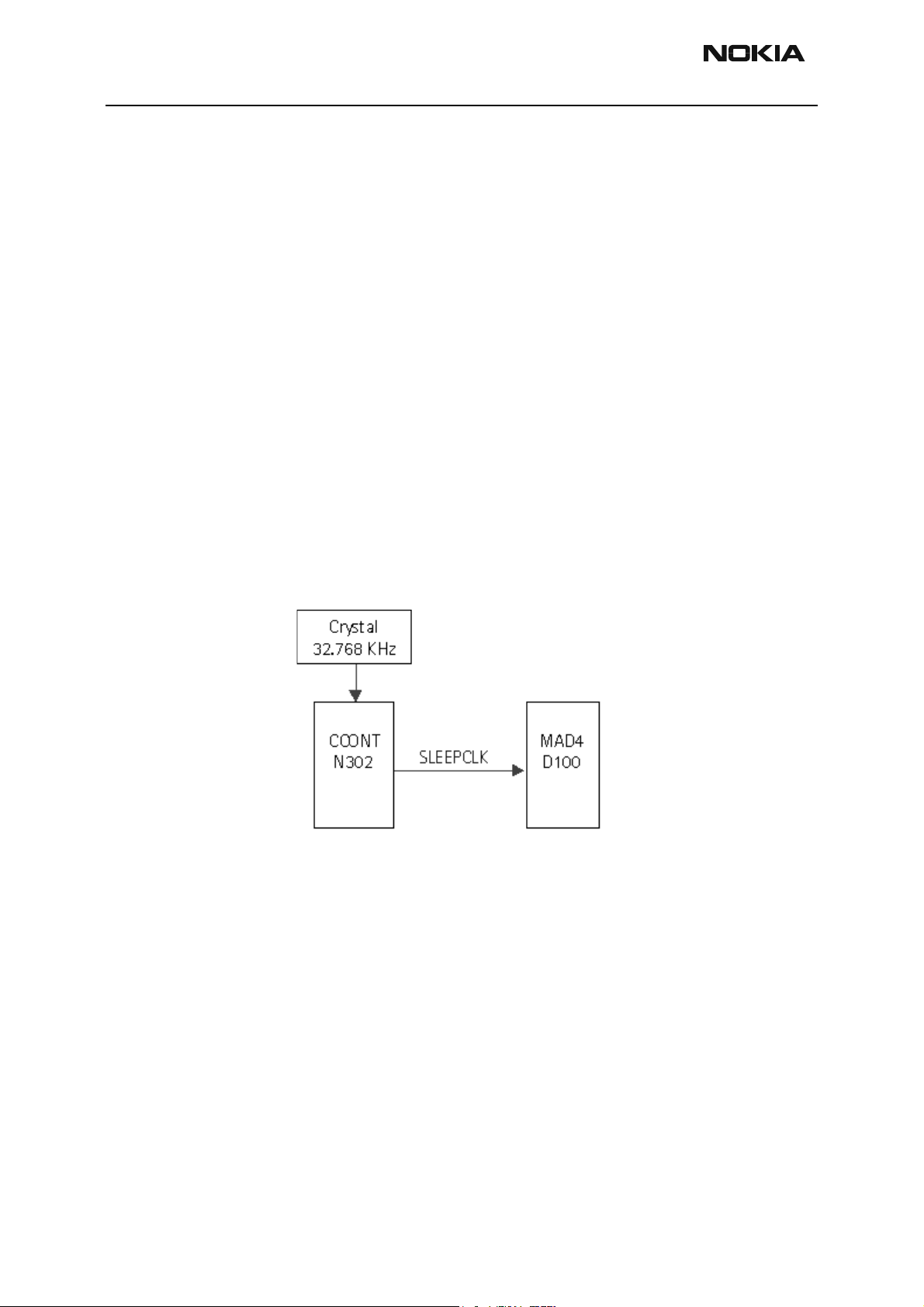
Sleep Clock
The 32kHz sleep clock is generated by CCONT, and can be checked at TPD32. The 32kHz
square wave will be present only after the phone is turned on.
System Clock
The 19.2MHz system clock is generated by the VCTXO in the RF section, and then squared
in CAFE. Check TPD11, which should be a 2.8V squarewave. This clock is not active during
the phone’s sleep mode (CLK_EN is low during sleep mode).
CDMA Clock
The CDMA clock is 9.8MHz and is generated in CAFE with a PLL. This should be a 2.8V
squarewave and can be verified at TPD10.
Charging Circuit
The charging switch, CHAPS, is controlled by a PWM from CCONT. This PWM can be at
Issue 1 05/02 Nokia Corporation Page 7
Page 8
NSD-5
10. Troubleshooting P AMS Technical Documentation
1Hz or at 32Hz, with varying duty cycles, and should only be active when a charger is
detected. The frequency depends on charger type. To verify correct operation of CHAPS,
monitor the charging current (ICHAR) with the service software. When the PWM is off,
current should be approximately 200uA. When the PWM is on, it must be greater than
approximately 300mA.
CAFE
The CAFE ASIC performs various functions with respect to the RF circuitry and audio. It
digitizes the analog voice signals from the microphone as well as converts received digital data to voice signals to be sent to the earpiece. This also includes accessory microphones and speakers. It also generates and decodes I and Q data for CDMA signals. CAFE
also acts as a clock squaring circuit and CDMA clock generator.
Microphones
The internal microphone is biased using transistor V280, which is powered by VR1_SW.
MICP should be about 1.7VDC, and MICN should be about 0.4VDC. Internal microphone
bias should only be active during a call. The XMIC is biased by the AUXOUT signal
through R240 and R241. The AUXOUT output provides 1.5V bias voltage to the external
microphone.
Earpiece and XEAR
The internal earpiece is driven differentially (EARP and EARN). The DC voltage on these
two pins is 1.35V. The difference in the DC voltage between these two pins should not be
more than 50mV.
The XEAR signal drives audio to the external accessories. The CAFE signal name is HF. The
DC level on this pin should be 1.35V. HFCM should also be at 1.35V. The difference in DC
voltage between these two pins should not be more than 50mV.
Note that SGND is the return path for XMIC and XEAR.
Transmit and Receive RF Signals
In CDMA mode, receive I and Q channel RF signals [RXIQ(3:0)] come into CAFÉ pins.
C201, C202, C203, and C204 can also be checked for these signals since they are in series
with the CAFÉ pins. Transmit I and Q RF signals [TXIQ(3:0)] can be seen at C205, C206,
C207, and C208.
MAD4
The MAD4 ASIC is the core of the baseband functionality and basically contains the DSP,
MCU, and CDMA logic. The DSP is used to perform functions such as RF control, DTMF
tone generation, and implementation of the vocoder. The MCU is used to perform functions that do not require as much power — higher-level functions such as UI software
(key presses, backlighting, LCD functions, etc.) and mode control.
DSP
The DSP sends control signals to the RF via PDMs. In order to control RF parameters such
as TX_LIM_ADJ, a continuously variable analog signal must be used. Since the DSP out-
Page 8 Nokia Corporation Issue 1 05/02
Page 9

NSD-5
PAMS Technical Documentation 10. Troubleshooting
puts only digital signals, a PDM RC circuit is used to convert the digital output signal to
an average analog voltage. A PDM line will always have a series resistor followed by a
shunt capacitor. The output of the MAD4 PDM lines will appear as squarewave signals.
However, after the shunt capacitor, the signals will appear to be DC with perhaps a slight
ripple. The RC circuit acts as an integrator in order to yield the average value (DC) of the
squarewave signal.
The transmit data bus (TXD(7:0)) is 8 bits wide. In CDMA mode, this bus is multiplexed
between sending I and Q data. The signals required to transfer TX data are
CAFE_TX_GATE, CLK9M80, and IQSEL. CAFE_TX_GATE must be high to transfer data, and
the data is clocked by CLK9M80, which is running at 9.8MHz.
MCU
The MCU is used to perform functions that require less processing power than the DSP. It
runs UI software and mode control; interfaces to MBUS; downloads code to flash; reads
and writes the EEPROM; controls charging; and interprets A/D data from CCONT.
Memories
MAD4 interfaces to three memories — Flash, SRAM, and EEPROM. All of them are powered by 2.8V (Vbb). During Flash programming, Vpp (signal name is Vff_flash on schematic) is driven to Flash memory.
Issue 1 05/02 Nokia Corporation Page 9
Page 10
NSD-5
10. Troubleshooting P AMS Technical Documentation
Troubleshooting Instructions
The first thing to do is to carry out a thorough visual check of the module. Make sure
that there is no mechanical damage and that solder joints are okay. Most failures will be
the result of SMD errors. Common errors include: solder placed where it shouldn’t be,
parts sliding off their pads, or parts placed incorrectly. A good visual inspection will pinpoint a large percentage of failing phones.
Before changing anything, also check all supply voltages and the system clock/sleep
clock.
The Troubleshooting Instructions section contains five modules:
- How to check/fix the system/sleep clock
- How to check/fix the power supplies
- How to check/fix the flashing faults
- How to check/fix the audio faults
- How to check/fix the charger faults
Page 10 Nokia Corporation Issue 1 05/02
Page 11

NSD-5
PAMS Technical Documentation 10. Troubleshooting
Check System Clock
Figure 1: System clock picture
Issue 1 05/02 Nokia Corporation Page 11
Page 12

NSD-5
10. Troubleshooting P AMS Technical Documentation
Check Sleep Clock
Figure 2: Sleep clock picture
In the Field
Although solder joints may be adequate to pass manufacturing requirements, they may
not withstand mechanical stress or heat cycling. Cracked or broken solder may cause
failures to occur as the result of simple use. Reflowing some of the major components
may fix problems where the phone exhibits strange behavior (some buttons may not
work, the phone doesn’t ring, or the phone doesn’t power on).
Power Supplies
Measure the power supplies. Test points are illustrated in the baseband test points table
and the layout diagram.
Page 12 Nokia Corporation Issue 1 05/02
Page 13

NSD-5
PAMS Technical Documentation 10. Troubleshooting
Power up sequence test:
CCONT digital parts keep MAD4 in reset by keeping PURX down for a delay of 62ms.
Here is the start-up sequence picture:
Ch1 = PWRONX
Ch2 = SLEEPCLK
Ch3 = PURX
Ch4 = RESETX
Phone is Totally Dead
The phone doesn’t take current at all when the power switch is pressed or when the
watchdog disable pin (TPD331) is grounded.
Make sure that the battery voltage you use is within specification (i.e., 3.2 - 4.2V). If the
voltage is lower than that, CCONT hardware (N302) prevents power on.
If the battery voltage is within the specification, change the CCONT (N302).
High current: This indicates that the problem is likely the result of a shorted component.
Check the orientation of major components (including RF) and check for shorts. Likely
components are those that are powered directly from Vbat such as CCONT, the PAs, and
various capacitors.
Low current: This indicates that CCONT is now powering on. Verify CCONT circuitry.
Phone Won’t Power Up
Do a visual inspection. Verify that all parts are on the board correctly, and that none is
missing. Phone won’t power up often is related to VCTCXO solder joints cracking and no
19.2MHz to the BB.
Issue 1 05/02 Nokia Corporation Page 13
Page 14

NSD-5
10. Troubleshooting P AMS Technical Documentation
Check that the 32kHz clock turns on when attempting to power up.
Check the power circuitry. This includes Vbat, Vref, and all of the linear regulators.
Power Doesn’t Stay on or Phone is Jammed
If this type of fault occurs after flash programming, there are most likely open joints in
ICs. Solder the IC joints. Normally, the power will be switched off by CCONT(N302) after
30 seconds if the CCONT watchdog cannot be served by software. This updating can be
seen with an oscilloscope at CCONTCSX(TPD334). In normal cases, there is a short pulse
from “1” to “0” every 8 seconds.
Because of underfill, check the supply voltages, clock signals, and power sequence. If the
power sequence fails, there are some open connections under MAD4 or compomemory. If
everything appears to be correct, it is best to erase the flash memory and try to reput the
software to the phone again.
Flash Programming Fails
The flash programming can be done via flash connector X052 or via dedicated PCB pads
(J56,J57). In production, the first programming is done via flash connector. After this, the
flash connector is cut away; as a result, the programming must be done via PCB pads visible through the shield under the battery. The fault-finding diagrams for flash programming are shown in the start-up sequence diagram.
In the case of flash programming errors, the flash prommer may provide some information about a fault. The fault information messages could be:
- MCU doesn’t boot
- Serial clock line failure
- Serial data line failure
- External RAM fault
- Algorithm file or alias ID not found
- MCU flash Vpp error
Flash: Failure to flash is the main baseband failure. Check all the CCONT regulators,
especially Vbb, VR1, and VR6 for shorts. Check clocks and reset circuitry. Check for shorts
on the address, data, and chip enable lines on the memories and MAD4. If a short is
detected, it may be that it is beneath the BGA flash and may have to be replaced.
Note: Unfortunately there is no ROM software that can be run when the phone does not
flash. Typically, this software would be used to test all of the interfaces between MAD4
and its peripherals. Therefore, it must be visually (or by ohmeter) determined whether
there is a possible short between two or more of the address or data lines.
Audio failures
If audio fails to be heard from the earpiece (or XEAR), check the following:
Check earpiece contacts.
Page 14 Nokia Corporation Issue 1 05/02
Page 15

NSD-5
PAMS Technical Documentation 10. Troubleshooting
Verify that the CAFÉ EARP and EARN bias is on. If necessary, check the entire receive
path—Rx voice data comes from the RF through the RXIQ bus (CDMA), then to MAD4
through RXD (11:0) (Refer to schematic).
The Rx voice data then goes back to CAFE on CAFESIO (0), and then to the earpiece or
XEAR. CAFESIO (2) must also be active.
Conversely, if the transmit audio is not working, the fault could be anywhere in the
transmit path. Check the following:
Check microphone contacts.
Microphone bias.
Tx voice data is transferred from CAFÉ to MAD4 on CAFESIO (1). CAFE-SIO (2) must also
be active. Tx voice data is then sent back to CAFÉ on the TXD bus (See schematic).
Tx voice data is then sent to RF on the TXIQ bus.
Issue 1 05/02 Nokia Corporation Page 15
Page 16

NSD-5
10. Troubleshooting P AMS Technical Documentation
Page 16 Nokia Corporation Issue 1 05/02
Page 17

NSD-5
PAMS Technical Documentation 10. Troubleshooting
Issue 1 05/02 Nokia Corporation Page 17
Page 18

NSD-5
10. Troubleshooting P AMS Technical Documentation
Battery Will Not Charge
If the battery won’t charge (phone doesn’t allow the battery to charge), check CHAPS
and the charging circuit. It may also be necessary to verify the A/D functionality of
CCONT since this is the method of detecting battery type, charger type, etc.
Page 18 Nokia Corporation Issue 1 05/02
Page 19

NSD-5
PAMS Technical Documentation 10. Troubleshooting
Baseband Test Points
Test
point
1 VSIM CCONT regulator output (2.8V-3.2V) From CCONT to FLASH
2 V5V CCONT regulator output (typical 5V) From CCONT to RF transmitter
3 EEPROMSDA EEPROM access serial data From MAD4 to EEPROM
4 EEPROMSCLK EEPROM access serial clock From MAD4 to EEPROM
5 CCONT_INT CCONT interrupt From CCONT to MAD4
6 MBUS Maintenance bus serial signal Bi-directional serial bus to MAD4
7 FBUS_TX Flash bus Tx signal Serial bus from MAD4 to the bot-
8 FBUS_RX Flash bus Rx signal Serial bus from the bottom con-
9 PWM PWM From CCONT to CHAPS
10 CLK9M83 9.83MHz square waveform From CAFE to MAD4
11 CLK19M20 19.2MHz square waveform From CAFE to MAD4
Signal name General characteristics General signal destination
and the bottom connector
tom connector
nector to MAD4
12 DATA(0) Data bus(0) From MAD4 to FLASH and SRAM
13 ADD(0) Address bus(0) From MAD4 to FLASH and SRAM
14 MEM(2) Write enable signal (active low) From MAD4 to FLASH, SRAM
15 MEM(1) SRAM select signal From MAD4 to SRAM
16 MEM(0) FLASH ROM select signal From MAD4 to FLASH
17 MEM(3) Read enable signal (active low) From MAD4 to FLASH, SRAM
18 RESETX Reset signal (active low) From MAD4 to CAFE
19 PWRONX Power ON (active low) From UI power key to MAD4 and
CCONT
20 CLK_EN VCTCXO enable signal From MAD4 to FLASH, CCONT, and
CAFE
21 UIF_CCONT_SCLK LCD and CCONT serial bus clock From MAD4 to LCD and CCONT
22 PURX Power up reset signal (active low) From CCONT to MAD4
23 SLEEPCLK 32.768KHz typical square waveform From CCONT to MAD4
24 CCONTCSX CCONT chip select signal From MAD4 to CCONT
25 UIF_CCONT_SDIO LCD and CCONT serial bus data From MAD4 to LCD and CCONT
26 WD_DIS Watchdog disable (active low) CCONT test point for phone diag-
nosis mode
27 Vmad MAD4 supply voltage From CCONT to MAD4
Issue 1 05/02 Nokia Corporation Page 19
Page 20

NSD-5
10. Troubleshooting P AMS Technical Documentation
Test
point
28 Vref CCONT regulator output (typical 1.244V) From CCONT to CAFE and battery I/
29 CRB 32.768KHz From 32K crystal to CCONT
30 Vbb Baseband supply voltage (2.8V typical) From CCONT to MAD4 and memo-
31 VR3 CCONT regulator output 2(typical 2.8V) From CCONT to RF receiver
32 VR4 CCONT regulator output 2(typical 2.8V) From CCONT to RF transmitter
33 VR2 CCONT regulator output 2(typical 2.8V) From CCONT to RF receiver
34 VR5 CCONT regulator output 2(typical 2.8V) From CCONT to RF transmitter
35 VR6 CCONT regulator output 2(typical 2.8V) From CCONT to CAFE
36 VR1 CCONT regulator output 2(typical 2.8V) From CCONT to 19.2MHz VCTCXO
37 VR1_SW 2.75V (MIC bias) From CCONT to V201 to CAFE
38 Vbat Battery voltage (3.2-4.2V)
Signal name General characteristics General signal destination
F
ries
From battery to CCONT and other
(3.1-5.2V with charger connected)
various parts of the phone
39 L_GND 0V From bottom connector through an
inductor to phone ground
40 V_IN Charger input (ACP-8:6V, LCH-9:8.3V
typical)
41 MICP Mic differential positive signal From bottom connector to CAFE
42 MICN Mic differential negative signal From bottom connector to CAFE
43 EAD_HEADINT Headset interrupt signal From bottom connector to MAD4
44 XEAR External ear output From CAFE to bottom connector
45 XMICN Mic external signal From bottom connector to CAFE
46 XMICP Mic external signal From bottom connector to CAFE
47 VR7 CCONT regulator output 2(typical 2.8V) From CCONT to RF transmitter
From bottom connector to CHAPS
internal microphone input
internal microphone input
external microphone input
external microphone input
Page 20 Nokia Corporation Issue 1 05/02
Page 21

NSD-5
PAMS Technical Documentation 10. Troubleshooting
Baseband Test Point Layout (Top side view)
Issue 1 05/02 Nokia Corporation Page 21
Page 22

NSD-5
10. Troubleshooting P AMS Technical Documentation
Baseband Test Points Layout (Bottom side View A)
Page 22 Nokia Corporation Issue 1 05/02
Page 23

NSD-5
PAMS Technical Documentation 10. Troubleshooting
Baseband Test Points Layout (Bottom side View B)
Issue 1 05/02 Nokia Corporation Page 23
Page 24

NSD-5
10. Troubleshooting P AMS Technical Documentation
RF Troubleshooting
Purpose
This section is intended to help the troubleshooter quickly determine and fix problems
with NSD-5 phones that have failed in the field.
Introduction
This document is written for use in conjunction with the WinTesla Tuning and Testing
software. Screen shots of the menu structures are shown throughout the document. This
document should be used in conjunction with the phone’s schematics which are referred
to in detail throughout.
WinTesla has three key menus:
Configure — Basic set up covered in WinTesla General Set Up
Testing — This menu allows switching on the phone in different modes
Tuning — This menu allows tuning and storing of data to eeprom
Tuning is described in four parts:
A description of the tuning: Describes the tuning process
Definition of result: What tuning is storing to eeprom
Manual Verification: How to use WinTesla to tune the phone
Troubleshooting: Outlines key components to be checked
Reference Documents
The phone’s schematics are essential for troubleshooting and are referred to in detail
throughout the document.
The following document may also be useful as a reference:
DRK00009-EN: Diagnostic Technicians Guide to Zim Flash/Alignment and Final/UI Tuning
and Testing
Page 24 Nokia Corporation Issue 1 05/02
Page 25

NSD-5
PAMS Technical Documentation 10. Troubleshooting
WinTesla General Set Up
Following connection of the phone to the PC COM port and starting WinTesla, select
Product from the main WinTesla menu and New from the drop-down menu. The ZIM
configuration will automatically be selected.
Select Configure from the main WinTesla menu and then choose Frequency Planning
from the drop-down menu. You then will be able to set up the default CDMA Channels.
The cable loss also should be entered. It is possible to enter a Tx and Rx cable loss separately; however, if a single cable is being used, then both losses should be the same.
CDMA Fault-finding Set Up
CDMA testing is started by selecting Testing from the main WinTesla menu and then
Issue 1 05/02 Nokia Corporation Page 25
Page 26

NSD-5
10. Troubleshooting P AMS Technical Documentation
selecting CDMA Tests from the drop-down menu. The “CDMA Testing” dialog box default
switches on both the transmitter in Rh
receiver ON, with the channel defined as “Mid” in the “Frequency Planning” dialog box.
PDMs may be adjusted on the “CDMA Testing” dialog box with the slider bars or by
entering a value in the appropriate boxes. The transmitter is switched off by inserting a
checkmark in the TX Off box. The Rho box switches on the CDMA IQ modulation. The
RX_IF_AGC is read by clicking the Read button. The LNA defaults to ON and can be
switched off by inserting a checkmark in the LNA box.
o mode (Tx with CDMA modulation) and the
Synthesizer Tuning Menu
WinTesla prompts you with equipment settings for all the tunings. At the end of the tuning sequence, WinTesla gives you the option of saving the new tuning values to EEPROM
or of exiting without saving the new values to EEPROM.
Tuning AFC
Description of Test
This test tunes the VCTCXO to exactly 19.2MHz using a DC voltage (C519 or TPD205)
controlled by the AFC PDM. The resulting PDM is stored to EEPROM. The CDMA IQ mod-
Page 26 Nokia Corporation Issue 1 05/02
Page 27

NSD-5
PAMS Technical Documentation 10. Troubleshooting
ulation is switched off. The output carrier is monitored with a spectrum analyzer. Click
on WinTesla Help for equipment set-up. The AFC PDM is tuned until the RF CW carrier
frequency is within +/-250Hz of 2073.1MHz (i.e., Channel 300).
Note: The Spectrum Analyzer must be connected to a high-stability, 10MHz reference at
the rear of the instrument. If this is not done, then the tuning will not be accurate.
Definition of Result
As a result of this tuning, the AFC PDM is stored to EEPROM, which puts the VCTCXO at
the correct frequency.
Manual Verification
Use WinTesla as follows:
1. Select Tuning from the WinTesla main menu and choose 1900 PCS and AFC... from
the drop-down menus.
2. The “Tuning AFC” dialog box is displayed. Use this box to adjust the Present AFC values, using the U
3. Select either the Save & Exit button or the No Save & Exit button when through.
p and Dn buttons or the PgUp or PgDn buttons.
Synthesizer Troubleshooting
The VCTCXO reference designator is G501. VR1 supplies 2.7V to the VCTCXO through
R501, decoupled with C561. The VCTCXO is controlled by a DC level from the AFC PDM in
MAD, connected to Pin1. The PDM is filtered by R141 and C141 in the baseband section
and by R504 and C507 in the RF section. Typically, a correctly tuned VCTCXO should have
approximately 1.5 volts on Pin 1.
Issue 1 05/02 Nokia Corporation Page 27
Page 28

NSD-5
10. Troubleshooting P AMS Technical Documentation
Adjustment of the AFC PDM from 0 to 511 should result in a voltage change on G501
Pin 1 of between 0.77 and 2.09 volts with approximately 45kHz change in the transmitter output frequency in the PCS band.
Selecting the “PCS AFC Tuning On” box disables the CDMA modulation, allowing AFC
tuning to be performed on the RF carrier feed through.
Page 28 Nokia Corporation Issue 1 05/02
Page 29

NSD-5
PAMS Technical Documentation 10. Troubleshooting
Test Points
Test Point Signal Name General Characteristics General Signal Destination
C507-R504 AFC VCTCXO control voltage PDM from MAD4
R530-R501 VR1 2.7V supply to VCTCXO CCONT to VCTCXO
C519-C544 19.2MHz 19.2MHz from VCTCXO output VCTCXO output to CAFE and PLL IC’s
C518 Tx VHFLO VHF LO to TIF CELL CDMA 346.2MHz LO from PLL to TIF IC
C517 Rx VHFLO 256.2MHz VHF LO to RIF LO from PLL to RIF
19.2MHz measured at the output of the VCTCXO with a 10 Mohm probe. The figure
below shows the 19.2MHz signals measured by oscilloscope.
Requirements
Test Point Signal Name Specification
C507-R504 AFC 1.5 +/- 0.5V
C519-C544 19.2MHz 19.2MHz +/- 150Hz
C518 Tx VHF LO >
C517 Rx VHF LO >
C510 TX UHF LO >
C524 RX UHF LO > -5dBm
-20dBm
-12dBm
-5dBm
Trouble Case 1: Tx VHF LO Power < -20dBm
Check the DC level of V508.
DC level of pin 1 > 1V, pin2 0.7 -0.8V, pin 3 > 2V, between Pin 1 and Pin 2 from 0.6 to
0.8V
If not, change V508.
Issue 1 05/02 Nokia Corporation Page 29
Page 30

NSD-5
10. Troubleshooting P AMS Technical Documentation
Trouble Case 2: Rx VHF LO Power < -12dBm
Check the DC level of V506.
DC level of Pin 1 > 1V, Pin 2 0.7 0.8V, Pin3 > 2V, between Pin 1 and Pin 2 from 0.6 to
0.8V
If not, change V506.
Trouble Case 3: UHF LO Power < -5dBm
Check the DC level of V502.
DC level of Pin 1 > 0.5V, between Pin 1 and Pin 2 from 0.6 to 0.8V
If not, change V502.
Trouble Case 3: Rx UHF LO Power < -5dBm
Change G502.
Page 30 Nokia Corporation Issue 1 05/02
Page 31

NSD-5
PAMS Technical Documentation 10. Troubleshooting
Start
Set to "Tuning A FC" Mode
Measure Antenna Port Frequency
=2073.1M Hz
+ / - 250Hz
Yes
Measure "CLK19M2RF" frequency
=19.2MHz + / -
150Hz
Yes
TX V H F L O te s t -> A
RX VH F L O te s t -> B
TX/R XUH F L O te s t - > C
No
No
Adjust AFC Value
Adjust AFC Value
A B C
Issue 1 05/02 Nokia Corporation Page 31
Page 32

NSD-5
10. Troubleshooting P AMS Technical Documentation
A
Measure TX VHF LO power at C518
> -20dBm B
No
Measure DC level of V508
pin 1>1V
pin2 >0.6V
pin3 >2V
Yes
Yes
No
Check
C515, C518, C511, L506
Change the V508
Page 32 Nokia Corporation Issue 1 05/02
Page 33

NSD-5
PAMS Technical Documentation 10. Troubleshooting
B
Measure RX VHF LO power at C517
> -12dBm
No
Measure DC level of V506
pin 1>1V
pin2 >0.6V
pin3 >2V
Yes
Yes
No
Change the V506
C
Check
C516, C517, C506, C569, L501
Issue 1 05/02 Nokia Corporation Page 33
Page 34

NSD-5
10. Troubleshooting P AMS Technical Documentation
C
Remove C704
Measure RX UHF
LO power at C524
> -5dBm
No
Measure DC level of
G502
pin 10>2 .7 V
Yes
Change G502
Set to CH300 in CDMA Tes ti ng mo de
Measure RX UHF LO frequency at
C524
=2088.1MHz
@ Ch600
+/-150Hz
Yes
Add C704
No
Yes
Measure SYN_LE1,
SYN_DAT, SYN_CLK
Displayed
waveforms?
No
D
Check MAD4
Page 34 Nokia Corporation Issue 1 05/02
Page 35

NSD-5
PAMS Technical Documentation 10. Troubleshooting
C
Remove L619
Measure TX UHF LO power at
Measure DC level of G502
Meas ure power level
C510
> -5dBm
No
pin 9 >2 .7V
Yes
at R517
> -5dBm
Yes
Set to CH300 in CDM A Testing Mode
Measure TX UHF LO frequency at C510
=2088.1MHz
@ Ch600
+/-150Hz
Yes
Add L619
No
No
Measure
SYN_LE1,
SYN_DAT,
SYN_CLK
Displayed
waveforms?
No
Yes
Measure DC level of V502
C521, C510, R517, R518, R516
TX Tuning
Description of Test
The RIF and TIF AGC is approximately a second-order curve; this curve is split into
16 segments for both Transmitter and Receiver. Offset and slope values are stored in
EEPROM for each of these 16 segments. The offset for the segments is computed from
Yes
pin 1> 0.5 V
Yes
Check
Check MAD4
Change G 50 2
No
Change the V502
END
Issue 1 05/02 Nokia Corporation Page 35
Page 36

NSD-5
10. Troubleshooting P AMS Technical Documentation
the 3-point calibration performed in this test. Then a second-order approximation is
made and the offset and slope computed.
TX_IF_AGC must be adjusted to achieve the correct power level for Point 1. When this is
done, the process must be repeated for Points 2 and 3.
Definition of Result
The results of the three-point tuning are the 16 slope and offset values, which are stored
to EEPROM RF_TUNE_PCS_TX_AGC_OFFSET_SLOPE_HANDLE.
Manual Verification
Use WinTesla as follows:
Page 36 Nokia Corporation Issue 1 05/02
Page 37

NSD-5
PAMS Technical Documentation 10. Troubleshooting
Issue 1 05/02 Nokia Corporation Page 37
Page 38

NSD-5
10. Troubleshooting P AMS Technical Documentation
TX Troubleshooting Flowchart
Start
Set Tx to ON
Check LED OFF
Set Tx_IF_GAIN = 500
Measure the total current
>550mA
No
Set TX_IF_GAIN = 10
<250mA
No
Measure UHF_LO
<-8dBm
No
Measure VHF_LO
<-15dBm
No
Set TX_IF_GAIN = 500
Yes
Replace RF connector or duplexor
START
Yes
Replace PAM
START
Yes
See Synthesizer troubleshooting processor
Yes
See Synthesizer troubleshooting processor
Measure Tx_IF signal
Yes
<-15dBm
No
1
Replace TIF
START
Page 38 Nokia Corporation Issue 1 05/02
Page 39

NSD-5
PAMS Technical Documentation 10. Troubleshooting
1
Set Tx to
Measure voltage at N606 pin2 and pin3
>0.5V
Measure RF signal level at N606 output pin8
>-20dBm
Measure voltage at V609 pin 1
Yes
Replace Replace
Start
Replace
Yes
<1.8V
Measure voltage at V606 pin 5
Yes
<2.5V
See synthesizer troubleshooting processorStart
No
No
Yes
No
Yes
No
No
Start
Replace
Start
Replace
Replace
Measure RF output signal level at V609 pin3<0.6VMeasure voltage at V609 pin 3
Yes
Measure voltage at V603 pin 7
Yes
Measure voltage at N603 pin 6
Start
Start
<-10dBm
No
<0.5V
No
Yes
<0.5VSee Baseband troubleshooting processor
No
Measure voltage at N602 pin 3
Yes
Replace
Start
<2.5V
No
2
Issue 1 05/02 Nokia Corporation Page 39
Page 40

NSD-5
r
r
10. Troubleshooting P AMS Technical Documentation
2
Measure the difference RF power level at N602 pin 2 and RF power level at N602 pin 4
Yes
<12dB
No
Measure voltage at V604 pin3
Yes
>4.7V
END
StartReplace V602
No
Measure voltage at V604 pin 3
Yes
<4.9V
No
Measure voltage at V603 pin 4
<2.5V
No
Replace V604
Start
See baseband troubleshooting processo
Yes
See baseband troubleshooting processo
1900 PCS Tuning Rx IF AGC
Description of Test
The RIF and TIF AGC is approximately a second-order curve. This curve is split into
16 segments for both transmitter and receiver. Offset and slope values are stored in
Page 40 Nokia Corporation Issue 1 05/02
Page 41

NSD-5
PAMS Technical Documentation 10. Troubleshooting
EEPROM for each of these 16 segments. The offset for the segments is computed from
the three-point calibration performed in this test. Then, a second-order approximation is
made and the offset and slope computed.
This tuning is done by putting signal level 1 into the receiver. The RX_IF_AGC will then
automatically adjust for max CAFE input and the RX_IF_AGC is noted. This process is
then repeated for signal levels 2 and 3.
Definition of Result
The results of the three-point tuning are the 16 slope and offset values, which are stored
to EEPROM RF_TUNE_PCS_RX_AGC_OFFSET_SLOPE_HANDLE.
Manual Verification
Use WinTesla as follows:
Issue 1 05/02 Nokia Corporation Page 41
Page 42

NSD-5
10. Troubleshooting P AMS Technical Documentation
1900 PCS Tuning Rx IF Compensation
Description of Test
In this tuning, the receiver is calibrated at five different frequencies across the band.
WinTesla instructs the signal generator to be set at five specific frequencies and a fixed
amplitude. The RX_IF_AGC is adjusted by the phone’s software to make the best use of
the CAFE ADC. The setting of RX_IF_AGC then is read from the phone at each of the five
frequencies.
Definition of Result
The five different values of RX_IF_AGC are stored to EEPROM.
Page 42 Nokia Corporation Issue 1 05/02
Page 43

NSD-5
PAMS Technical Documentation 10. Troubleshooting
Manual Verification
Use WinTesla as follows:
Issue 1 05/02 Nokia Corporation Page 43
Page 44

NSD-5
10. Troubleshooting P AMS Technical Documentation
Page 44 Nokia Corporation Issue 1 05/02
Page 45

NSD-5
PAMS Technical Documentation 10. Troubleshooting
RX Troubleshooting
Troubleshooting
Check components in the receiver chain from Duplexer Z727, LNA V701 and Mixer N701,
the 128.1MHz CDMA IF SAW filter Z728 and RIF N730. Check that the RX_IF_AGC RIF
Pin D2 changes as the receiver input signal level is adjusted. Check the Rx VHF LO RIF
C517. See plot diagram (following) and the Synthesizer Block.
Note: If any of these components are damaged and are replaced, then the Rx IF AGC second-order
curve must be returned.
Issue 1 05/02 Nokia Corporation Page 45
Page 46

NSD-5
10. Troubleshooting P AMS Technical Documentation
Rx VHF LO Measured at RIF Pin 20 with a Hi Z Probe
RX Troubleshooting Flowchart
Start
Measure the RF signal power gain
between V701 pin 1 and pin 3
See Baseband
troubleshooting
processor
>-10dB
Measure the Freq. of N701
Check the N730 Pin D1
No
>2.0V
Yes
Replace N730 Replace N730
No No
Pin6
128.1 MHz
Count Value
charged by RF_RX
level charging
End
No
Yes
No
Yes
Yes
Check the voltage at V701
Pin3 is>2.0V & Replace V701
Measure UHF_LO Power level at
N701 Pin4
See synthesize
No
Yes
troubleshooting
See synthesize
No
troubleshooting
>-10dBmCheck the RX_Count by WinTesla
Yes
Replace N701
Measure VHF_LO Power level
at N730 Pin D6
>-10dBm
processor
processor
Test Points
Signal Name General Characteristics General Signal Destination
AFC VCTCXO control voltage PDM from MAD4
VR1 2.7V supply to VCTCXO CCONT to VCTCXO
19.2MHz 19.2MHz from VCTCXO buffer VCTCXO buffer to CAFE and PLL IC’s
TX_LIM_ADJ Detector demand voltage PDM from MAD4 Pin 128 deector
circuit at RF output
1900 MHz PA Output RF output from PA check for short
RF output from PA
with phone switched OFF
Page 46 Nokia Corporation Issue 1 05/02
Page 47

NSD-5
PAMS Technical Documentation 10. Troubleshooting
Signal Name General Characteristics General Signal Destination
Tx VHF LO VHF LO to TIF PCS CDMA
436.2MHz
Tx UHF LO UHF LO up converter IC LO from 2GHz VCO to up converter
Rx VHF LO 256.2MHz VHF LO to RIF LO from PLL to RIF
RX_IF_AGC DC voltage proportional to signal
level into receiver in CDMA mode
LO from PLL to TIF IC
IC
AGC control voltage from MAD4
Pin A16 to RIF Pin D2
Issue 1 05/02 Nokia Corporation Page 47
Page 48

NSD-5
10. Troubleshooting P AMS Technical Documentation
Page 48 Nokia Corporation Issue 1 05/02
 Loading...