

Page 1

Programs After Market Services (PAMS)
Technical Documentation
Chapter 3
NHE–6 TRANSCEIVER
OVERVIEW
Original 06/97
Page 2

NHE–6
After Sales
Transceiver Overview
Technical Documentation
CHAPTER 2 – TRANSCEIVER OVERVIEW
Contents
Introduction Page 3–3
Block Diagram of External Connections Page 3–3
Modes of Operation Page 3–4
Circuit Description Page 3–4
Block Diagram Page 3–5
Power Distribution Page 3–5
Power Distribution Diagram Page 3–6
Page 3–2
Original 06/97
Page 3
After Sales
NHE–6
Technical Documentation
Introduction
The NHE–6 is a radio transceiver unit for the pan–European GSM network. It
is a GSM (phase 2) power class 4 transceiver providing 15 power levels with a
maximum output power of 2 W.
The transceiver consists of a Radio module (GJ8A), UIF–module (GU8) and
assembly parts
The plug–in (small size) SIM (Subscriber Identity Module) card is located inside
the phone.
Block Diagram of External Connections
EARPIECE
2
SIM Display
UI–module
MIC
2
Transceiver Overview
26
10
30
5
Keypad
RADIO MODULE
12
SYSTEM
CONNECTOR
2+2
CHARGER
2
BUZZER
4
BATTERY
2
ANTENNA
Original 06/97
BOTTOM CONNECTOR
Page 3–3
Page 4

NHE–6
After Sales
Transceiver Overview
Modes of Operation
There are four different operation modes
– power off mode
– idle mode
– active mode
– local mode
In the power off mode only the circuits needed for power up are supplied.
In the idle mode circuits are in reset, powered down and clocks are stopped as
long as possible.
In the active mode all the circuits are supplied with power although some parts
might be in the idle state part of the time.
The local mode is used for alignment and testing.
Circuit Description
Technical Documentation
The transceiver electronics consists of the Radio Module (RF + BB blocks), the
UI–module and the display module. The UI–module is connected to the Radio
Module with a connector and display module is connected to UI–module by
solder joint. BB blocks and RF blocks are interconnected with PCB wiring. The
Transceiver is connected to accessories via a bottom system connector with
charging and accessory control.
The BB blocks provide the MCU and DSP environments, Logic control IC, memories, audio processing and RF control hardware (RFI2). On board power
supply circuitry delivers operating voltages for BB blocks. RF blocks have regulators of their own.
The general purpose microcontroller, Hitachi H8/3001, communicates with the
DSP, memories and Logic control IC with an 8–bit data bus.
The RF block is designed for a handportable phone which operates in the GSM
system. The purpose of the RF block is to receive and demodulate the radio
frequency signal from the base station and to transmit a modulated RF signal to
the base station.
Page 3–4
Original 06/97
Page 5

After Sales
NHE–6
Technical Documentation
Block Diagram
RX
RX
DUPLEX
FILTER
SYNTE
SYNTE
TX
TX
IF 13 M
Clk 13 M
AFC
TXI,TXQ
TXC
Transceiver Overview
SIM
PSCLD
RESET
RFI2
Keyboard
SYSTEM
ASIC
Clk
13 M
Display
RESET
Clk
13 M
Clk
13 M
RESET
MCU
DSP
RESET
M2BUS
FBUS
AUDIO
RF CONTROL
RF BLOCK
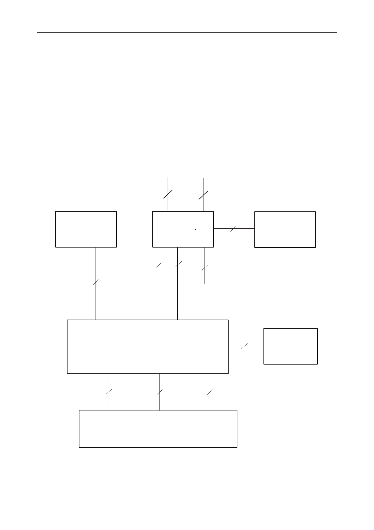
Power Distribution
The power supply is based on the ASIC circuit PSCLD. The chip consists of
regulators and control circuits providing functions like power up, reset and
watchdog functions. External buffering is required to provide more current.
The MCU and the PSCLD circuits control charging together, detection being
carried out by the PSCLD and higher level intelligent control by the MCU. Charger voltages as well as temperature and size of the battery are measured by
internal ADC of MCU or RFI (depending on the state of the phone). MCU measures battery voltage via DSP by means of RFI2 internal ADC.
The detailed power distribution diagrams are given in Baseband blocks and RF
blocks documents.
Clk 512 k,
Clk 8 k
SYSTEM BLOCK
Original 06/97
Page 3–5
Page 6

NHE–6
After Sales
Transceiver Overview
Power Distribution Diagram
BB–BLOCK
EXT.PWR. SUPPLY
PSCLD
3.0 ... 3.3 V
REGULAT O
R
4.5 V
UI–MODULE
AUDIO CODEC
CCP
U
MCU
RFI 2
Technical Documentation
TXPWR
RXPWR
BATTERY
5.5 ... 8.2 V
REGULATO
4.8 V
VCTCX
O
RF–BLOCK
VXOENA
R
SYNTHPWR
UHF PLL
VHF PLL
Buffer
REGULATO
R
4.8 V
RF LNA
IF AMP
TX buffer
Power cont
REGULATO
R
4.8 V
CRFRT
REGULATO
R
7 V
PWR AMP
Page 3–6
Original 06/97
Page 7

After Sales
NHE–6
Technical Documentation
Transceiver Overview
This page intentionally left blank.
Original 06/97
Page 3–7
 Loading...