

Page 1

Nokia Customer Care
RM-12 Series Transceivers
7 - System Module
Issue 1 11/2004 ©Nokia Corporation
Page 2

RM-12
System Module CCS Technical Documentation
[This page left intentionally blank]
Page 2 ©Nokia Corporation Issue 1 11/2004
Page 3

RM-12
CCS Technical Documentation System Module
Table of Contents
Page No
ABBREVIATIONS ....................................................................................................... 3
1EL System module....................................................................................................... 5
Baseband top-level description...................................................................................... 5
APE BB description .....................................................................................................5
APE Memories .............................................................................................................7
CMT BB description ....................................................................................................7
Memories on CMT side ...............................................................................................8
Baseband clocking and reset.......................................................................................... 8
APE clocking and reset ................................................................................................8
CMT Clocking Scheme ...............................................................................................9
Back-up battery and real time clock ............................................................................9
Baseband energy management....................................................................................... 9
CMT energy management ...........................................................................................9
APE energy management ............................................................................................9
Modes of operation ....................................................................................................10
Power distribution ......................................................................................................11
Current gauge .............................................................................................................12
APE discrete regulators .............................................................................................12
Audio............................................................................................................................ 14
Audio control signals .................................................................................................14
Audio modes ..............................................................................................................15
HP call..................................................................................................................... 15
IHF call.................................................................................................................... 15
Accessory call ......................................................................................................... 15
APE audio ............................................................................................................... 15
Internal interfaces......................................................................................................... 17
XBUS .........................................................................................................................17
XABUS ......................................................................................................................17
External SERIAL interfaces......................................................................................... 17
MMC INTERFACE ...................................................................................................17
USB INTERFACE .....................................................................................................17
SIM interface................................................................................................................ 17
Display interface .......................................................................................................... 17
Camera interface.......................................................................................................... 18
Touch screen interface ................................................................................................. 18
Keyboard interface....................................................................................................... 18
Bluetooth...................................................................................................................... 19
Flashing Interfaces....................................................................................................... 19
APE Flashing .............................................................................................................19
CMT Flashing ............................................................................................................19
Settings Database......................................................................................................... 19
Issue 1 11/2004 ©Nokia Corporation Page 3
Page 4

RM-12
System Module CCS Technical Documentation
ABBREVIATIONS
Table 1:
AAC Advanced Audio Coding
ACI Accessory Control Interface
APE Application processor engine
ASIC Application specific integrated circuit
ASIP Application specific integrated passive
BB Baseband
CMT Cellular mobile telephone
DAC Digital to analogue converter
DPLL Digital phase-locked loop
DSP Digital signal processor
EDGE Enhanced data rates for GSM evolution
EM Energy management
I2C
LCD Liquid crystal display
MDOC Disc-On-Chip
MMC Multi Media card
MP3 MPEG1 layer 3 audio compression format
MPU Microprocessor unit
NAND Sequential Access Flash Memory
NOR Random Access Flash Memory
OMAP1510 TI’s Open Multimedia Application Processor
PA Power amplifier
PURX Power-up reset signal
PWL Pseudo-noise pulse width light modulator
PWT Pulse width tone
Inter-integrated circuit control bus
RAM Random access memory
SRAM Static random access memory
SDRAM Synchronous dynamic random access memory
RF Radio frequency
ROM Read only memory
SD Secure Digital
Page 4 ©Nokia Corporation Issue 1 11/2004
Page 5

RM-12
CCS Technical Documentation System Module
Table 1:
SIM Subscriber identity module
SMPS Switched mode power supply
SPI Serial protocol interface
TC Traffic controller
UART Universal asynchronous receiver/transmitter
UEM Universal energy management
UPP Universal phone processor
USB Universal serial bus
XABUS Audio data transfer channel between the CMT and APE engines
XBUS Main communication channel between the CMT and APE engines
Issue 1 11/2004 ©Nokia Corporation Page 5
Page 6
RM-12
System Module CCS Technical Documentation
1EL System module
1EL System module is the engine board of the RM-12 phone. It includes the baseband and
RF functions of the phone.
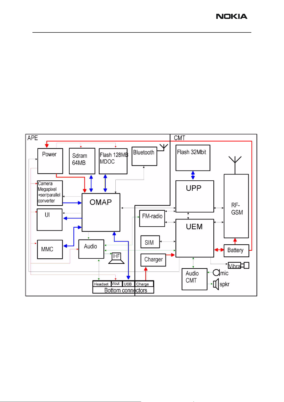
Baseband top-level description
Product RM-12 is a hand portable EGSM 900/ GSM 1800/1900MHz product for the mediaphone segment.
The RM-12 baseband consists of a dual-processor engine named as Cellular Mobile Telephone (CMT) and Application Processor Engine (APE) sides. The top-level block diagram is
presented below.
Figure 1: Baseband Block Diagram
APE BB description
APE (Application Processor Engine) in RM-12 includes not only the processor itself but
also the peripherals around it, clocking, resetting and power management for these
parts.
APE is based around OMAP1510 (Open Multimedia Application Platform) processor from
Texas Instruments. Peripheral attached to OMAP1510 include Audio DAC, Camera, Bluetooth, PDA display, touchscreen controller, memory card and external SDRAM and Flash
Page 6 ©Nokia Corporation Issue 1 11/2004
Page 7

RM-12
CCS Technical Documentation System Module
memories.
APE acts as system slave compared to CMT side. CMT holds the master reset and power
management logic. APE and CMT are connected through serial link called XBUS.
OMAP1510 has it’s own crystal (12MHz), but sleep clock is derived from CMT side (constantly running). This enables APE run almost independently from CMT.
The APE baseband has following components:
• 12MHz crystal
• LCD display interface
• 64MB Synchronous Dynamic Random Access Memory (SDRAM)
device
• 128MB MDOC flash device
• Bluetooth interface
• Audio Digital-to-Analog Converter (DAC) and audio power amplifier
(PA)
• Keyboard interface
• Pop-portTM bottom connector with USB interface, Accessory interface
and Battery charger interface
• Touch panel interface
• MMC interface
• Camera interface
Issue 1 11/2004 ©Nokia Corporation Page 7
Page 8
RM-12
System Module CCS Technical Documentation
APE Memories
APE memory system consists of 64Mbyte (32Mx16) SDRAM device connected to the
OMAP1510 fast external memory interface (EMIFF) and 128Mbytes (64Mx8) of MDOC
flash device connected to the OMAP1510 slow external memory interface - EMIFS.
MDOC flash is used as a boot device and mass memory. User data is stored to MDOC.
CMT BB description
Main functionality of the CMT baseband is implemented into two ASICs: UPP (Universal
Phone Processor) and UEM (Universal Energy Management).
Figure 2: CMT block diagram
RF-BB
IF
R&D
Test IF
JTAG
Ostrich
Memory
32Mb
Flash
RFConv
RFIC
Control
RF
Control
RFClk
CMT - APE interface
XBUS XABUS
PWREn
130ms delay +
1V8 -> 2V8 LS
PURX
RFConvIF
Internal SIM IF
Audio IF
MBUS
FBUS
DBUS
CBUS
FM radio
control
SleepClk
MIC+ACI
FM
Radio
"Antenna"
SleepClk
(2V8)
IRLEDC
IRTX
Prod/AS
Test IF
FBUS
MBUS
UEMKUPP 8M
UEM
XEAR
L+R
L+R
Zocus
32kHz
Audio
Audio
DAC
DAC
L+R
Audio
AMP
PWR key
Vibra
SIM
EAR
MIC
CHRG
current
sense
BATT. IF CHRG. IF
Control
from APE
Accessory
regulator
System Connector
IHF
The I/O voltage of CMT baseband is 1.8V and the analog parts are powered from 2.8V
power rails. The core voltage of UPP can be altered with SW.
Page 8 ©Nokia Corporation Issue 1 11/2004
Page 9

RM-12
CCS Technical Documentation System Module
Memories on CMT side
RM-12 CMT memory is 32Mbits of 54MHz NOR FLASH. The flash has also “Read While
Write” capabilities, thus enabling the SW based implementation of emulated EEPROM
within the flash.
Baseband clocking and reset
Figure 3: APE&CMT BB clocking
Display
Crystal
APE SYSClk
12MHz
BT
module
PCMCLK
267kHz
DOTClk
12.5MHz
SDRAMClk
75MHz
SDRAM
Audio
DAC
BCLK
12MHz
VCXO
RFClk
26MHz
OMAP1510 UPP UEM
I2S Clk
6MHz
MDOC
CamClk
12MHz
XABUS
12MHz
Camera
converter
FLASH
MMC
Camera
Helgo
SCU Clk
13MHz
32kHz 2.8V
CMT FlashClk
max 54MHz
FLASH
SleepClk
SleepClk 32kHz
CBUSClk 1MHz
DBUSClk 13MHz
SIMClk 3.25MHz
1.8/2.8 V level shifter
SIM
ZOCUS
I2C SCK
400 kHz
RF-ASIC
APE clocking and reset
The application engine has two separate clock sources: one for system clock (12MHz)
and one for sleep clock (32.768kHz), which is hereafter called Clk32k. The Clk32k is not
generated by the application engine, but is derived of the CMT SleepClk using a level
shifter. The Clk32k is running always when the engine is powered.
The 12MHz system clock is generated by OMAP1510. The crystal driver and related circuitry is internal to the processor and an external quartz crystal is used as a frequency
reference. The bluetooth clock is also derived of this clock using a clock buffer. Note that
the system clock is switched off during sleep mode.
The APE reset (MPU_nReset) is controlled by the CMT reset (PURX) generated by UEM.
PURX and MPU_nReset have different logic levels, but the latter is not simply a level
Issue 1 11/2004 ©Nokia Corporation Page 9
Page 10

RM-12
System Module CCS Technical Documentation
shifted version of the former. There is also an external delay circuit connected between
the PURX and MPU_nReset lines that keeps the APE reset active ca.130ms after CMT
reset is released. The delay circuit has no significant effect on falling edge timings, thus
both resets are activated simultaneously.
CMT Clocking Scheme
A 26 MHz system clock for the CMT is derived from the RF VCTCXO circuits.
The low frequency sleep clock is generated in UEM using an external 32.768kHz crystal.
The phone is waken up by a timer running from this 32 kHz clock supply. The sleeping
time is determined by network parameters. The sleep mode is entered when both the
MCU and the DSP are in standby mode and the normal 26 MHz VCTCXO clock has been
switched off.
When the CMT side is in sleep mode VCTCXO is off. In this mode 32.768 kHz sleep clock
generated by UEM is used as reference clock for the baseband.
Back-up battery and real time clock
CMT side runs the real time clock (RTC). A backup battery is connected to UEM RTC to
keep the clock running when main battery is disconnected.
Baseband energy management
BP-5L 1300 mAh Li-Po battery is used as main power source for RM-12.
RM-12 supports ACP-12 type of two-wire charger. Three wire chargers are treated as
two wire ones. There is not separate PWM output for controlling charger but it is connected to GND inside the bottom connector.
CMT energy management
CMT side Energy management is by UEM internal regulators.
APE energy management
On APE side there are several Linear and SMPS regulators to supply APE engine, UIHW
and other devices:
• Two DC/DC converters (National Semiconductor's LM2708) for generating 1.57V and 1.8V to OMAP1510 and memories
• One linear regulator for 2.8V APE side logic (National Semiconductor's
LP3981)
• One 3.0V linear regulator (National Semiconductor's LP3985) for powering of MMC card.
• One 3.3V linear regulator (National Semiconductor's LP2985) for powering the USB block of OMAP1510.
Page 10 ©Nokia Corporation Issue 1 11/2004
Page 11

RM-12
CCS Technical Documentation System Module
• One 2.5V linear regulator (National Semiconductor’s LP3990-2.5) for
powering the camera analog parts.
• One 1.5V linear regulator (National Semiconductor’s LP3990-1.5) for
powering the camera digital parts.
Modes of operation
The state machine in UEM controls mainly the operating modes of the engine. State
transitions are enabled by signals taken from UEM, UPP and OMAP1510. In the following
the modes are briefly discussed.
In general, the state transitions are based on the following information:
• Battery voltage (HW limits and cutoffs)
• Back-up battery voltage limits and cutoffs
• Power key status (The power key is connected to PWRONX pin of
UEM)
• Delays generated by the state machines
• Real time clock (RTC) alarms
• Watchdogs
• Thermal shutdowns
• SLEEPX signal from UPP
• LOW_PWR signal from OMAP1510
The device wakes up after the power key is pressed. Operation modes are briefly discussed below.
• NO_SUPPLY mode means that the main battery is not present or its
voltage is too low (below UEM master reset threshold limit) and back-up
battery voltage is too low.
• In BACK_UP mode the main battery is disconnected or empty, but
back-up battery has sufficient charge in it
• STANDBY mode is entered by power key to “Switch off” the device. To
the user it looks that device is fully off but in reality the early stages of
the full boot-up sequence have been executed and all automatically
started applications have been launched. In this mode the user interface
and the RF functions are switched off. CMT engine is in sleep and APE
is in deep sleep mode. By using power key device boots up back to
Issue 1 11/2004 ©Nokia Corporation Page 11
Page 12

RM-12
System Module CCS Technical Documentation
POWER_ON –mode.
• RESET mode is a synonym for start-up sequence and contains in fact
several modes. In this mode certain regulators and system oscillators
are enabled and after they have stabilized, the system reset (PURX) is
released and PWR ON mode entered.
• In POWER_ON mode SW is running and controlling the system
• SLEEP mode is entered only from PWR ON mode when system activity
is low. CMT and APE sides can be in sleep mode independently from
each other.
Power distribution
Figure 4: BB power distribution diagram
BATTERY
VIBRA
UEM
DLIGHT
VR1..7
VFLASH1
VFLASH2
VANA
VSIM
VIO
VCORE
LP3985-2.8
2.8V
LP3981-2.8
2.8V
LM2708
1.57V DC/DC
LM2708
1.82V DC/DC
LP3990-2.5
2.5V
LP3990-1.5
1.5V
TK11851
DC/DC
VMMC
LP3985-3.0
3.0V
PA RF
Various
7
I/O
I/O UPP
CORE
Pop-Port™
Vout USB(Vbus)
I/O
I/O
USB
CORE
I/O MEM
Control line
Battery line
Power line
LP2985-3.3
3.3V
OMAP1510
VPP FLASH
VCC
I/O
AUDIO PA
BT
Vregin, I/O
AUDIO DAC
TOUCH
FLASH
CORE, I/O
SDRAM
CORE, I/O
APE Display
CORE, I/O
BACKLIGHT
MMC
CAMERA
Analog
Digital
Page 12 ©Nokia Corporation Issue 1 11/2004
Page 13

RM-12
CCS Technical Documentation System Module
Current gauge
RM-12 uses current measurement chip (ZOCUS) used LM3820 to measure all current
drawn from and charged to battery. Current gauge reading is done by CMT side sw. It is
used to estimate the battery charge level presented as battery bars on the display.
Current is measured from the positive battery terminal using sense resistor. The sense
resistor is formed from PWB tracks arranged as 4-terminal resistor and LM3820 senses
voltage across the resistor.
APE discrete regulators
APE BB contains several discrete regulators. lists the output voltages, maximum output
currents, control signals and loads of the regulators.
Table 2: Discrete voltage regulators used in BB
Signal Regulator Vout (V) I (mA) Section Enabled By
V28 N4200
LP3981YDX-
2.8_NOBP
V33 N2001
LP2985AIM5X-
3.3_NOPB
VMMC N5200
LP3985ITLX-
3.0_NOPB
VOUT N2000
LP3985ITLX-
2.8_NOPB
V15 N4201
LM2708HTLX-1.57
NOPB
V18 N4202
LM2708HTLX-1.82
NOPB
2.8 ±3% 300 BT, OMAP1510, pullups, MMC- and Battery- door switch,
FLASH
UI (TP, display)
APE audio DAC
3.3 ±3.5% 150 USB transceiver GPIO(3)
3.0 ±3% 150 MMC GPIO(15)
2.8 ±3% 150 Pop-Port™ GENIO(28)
1.57 ±3% 415 OMAP1510 core VFLASH1
1.35 ±5% 45 In linear mode
1.82 ±3% 415 APE I/O, SDRAM,
FLASH
VIO
VIO
V15CAM N4204
LP3990YDX-
1.5_NOPB
V25CAM N4203
LP3990TLX-2.5_NOBP
1.82
±5%
1.5
±3%
2.5
±3%
45 In linear mode
150 GPIO(6)
150 GPIO(12)
Issue 1 11/2004 ©Nokia Corporation Page 13
Page 14

RM-12
System Module CCS Technical Documentation
VLED1+
VLED2+
D4420
TK11851LTL-G
10-12.5 36
2
Backlight
Keyled
Dlight
Majority of the regulators listed above are connected directly to VBAT. The only exception to this rule is V33 regulator, which is supplied by the USB Host via USB cable.
Page 14 ©Nokia Corporation Issue 1 11/2004
Page 15

RM-12
CCS Technical Documentation System Module
Audio
This section describes the audio HW. External audio components and acoustics are not
considered in detail in this section.
As BB is based on dual-processor architecture, also audios are divided to APE and CMT
parts. Audio control is mostly on APE side; phone audio is routed from CMT side to APE in
analog form. In CMT side audio HW is integrated into the UEM ASIC. In APE side most
important parts are OMAP1510, audio DAC and audio power amplifier.
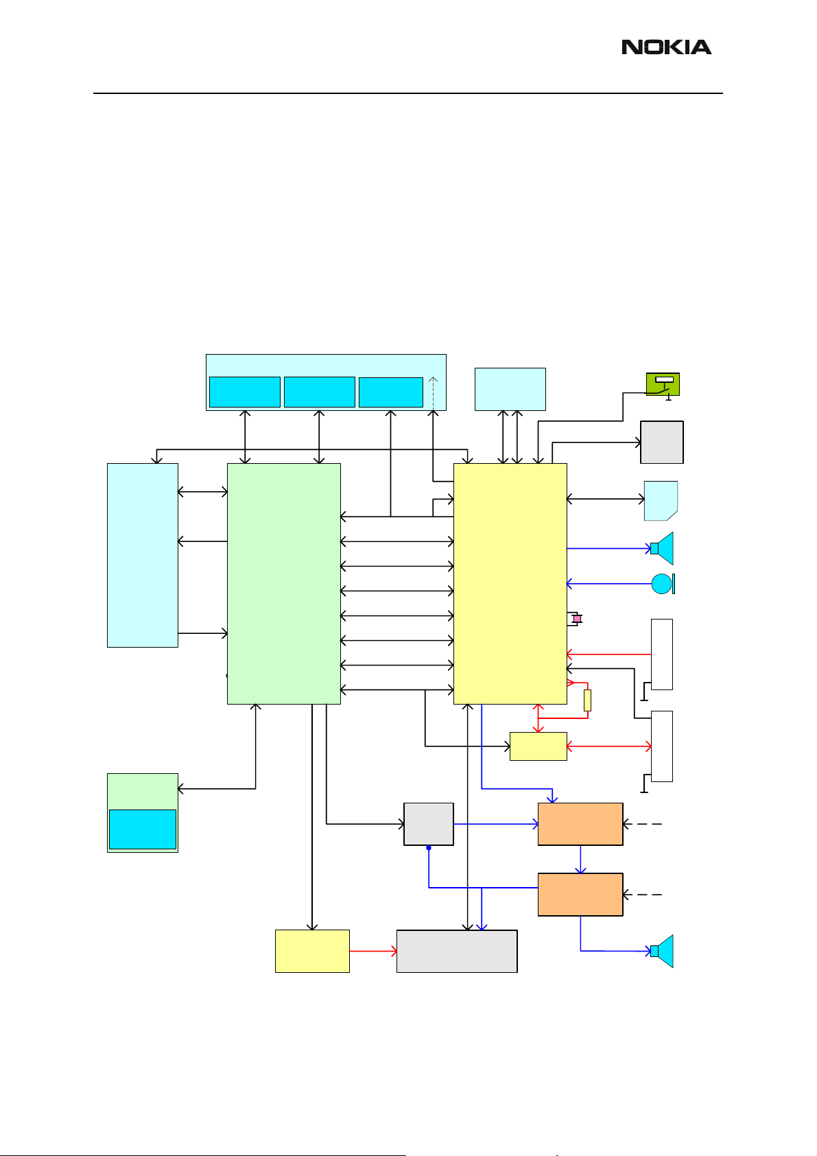
Figure 5: Audio architecture
DSP_SIO
XABUS,
4
4
PCM
CSR
BT
UPP
XBUS,
4
MCSI2
MCSI1
1
1
FM Radio Control,
Ringtones
Streaming
engine
OMAP 1510
MP3 decoder
Entertainment
effec ts
UEM
D
LP
A
D
LP
A
5
Stereo or mono
McBSP1
digital audio
I2CI/ F
McBSP2
MIC1
MIC2
MIC3
EARP/EARN
HF/HFCM
XEAR
TEA5767
R/MONO
L/MONO
I2S, Digital audio,
4
I2C Control,
2
2
1
1
1
-10dB
Phone_inIHF
Phone_inHS
RIn
Lin
4855
Mic_In
R_Line_In
1
L_Line _In
1
2
R_HP_Out
L_HP _Out
TLV320AIC 23B
McBS P Contro l, SPI Mo de,
R_Out
L_Out
3
1
-10dB
The stereo output of the audio power amplifier (4855) is designed for use with the
extended Pop-portTM connector. It also has a differential mono output for driving the
handsfree speaker.
IHFOut
ROut
LOut
2
2
2
2
Pop-p ort
The battery voltage (VBATT) is used directly as supply voltage for power amplifier. Nominal battery voltage is 3.7V.
The type of Audio DAC used is Texas Instruments TLV320AIC23B and the supply voltage
for this is coming from V28.
Audio control signals
Audio DAC is controlled via I2C bus by OMAP1510. Digital audio data from OMAP1510 to
Audio DAC is coming via MCBSP1.
The audio power amplifier is controlled through a 3-wire SPI bus (MCBSP2 of
OMAP1510). The audio power amplifier mode and gain values are controlled via SPI bus.
Issue 1 11/2004 ©Nokia Corporation Page 15
Page 16

RM-12
System Module CCS Technical Documentation
The HEADINT signal is needed for recognizing the external device (e.g. headset) connected to system. The recognition is based on the ACI-pin of the Pop-portTM, which is
shorted to ground inside the external device.
The button of the external device generates HOOKINT. This is used to answer or end a
phone call.
Audio modes
HP call
The basic audio mode is hand portable mode. This is entered when no audio accessories
are connected and handsfree mode is not selected.
A call is created by CMT. The internal ear piece is driven by the CMT engine for voice
calls. The internal microphone is driven by the CMT for voice calls and voice recording.
The internal microphone is enabled and uses the MICB1 bias voltage from UEM.
IHF call
This mode can be entered by user selection.
A call is created by CMT. The internal microphone is driven by the CMT for voice calls and
voice recording. The internal microphone is enabled and uses the MICB1 bias voltage
from UEM as in HP mode.
XEAR output of UEM is used to drive mono output signal is connected to the APE Audio
DAC. Signal is then routed to the Phone_In_IHF input of the 4855. This drives the internal speaker via the SPKRout driver.
Accessory call
This mode is used when accessory is connected to Pop-port
Call is created by CMT. The uplink signal is generated by external microphone and transferred to UEM MIC2 input (via XMIC signals from Pop-port
MIC2B bias voltage and MIC2P/N inputs are enabled on UEM.
As in IHF call down link audio signal is routed through the single ended XEAR output
driver in UEM. The mono XEAR output is connected to the DAC and then signal is routed
to the L
portTM connector using the L
TM
.
TM
connector). Hence the
and RIN inputs of the audio power amplifier. Accessories are driven via Pop-
IN
driver of audio power amplifier.
OUT
APE audio
This mode is entered when user starts the multimedia application (e.g. MP3, AAC etc.),
which is played via IHF speaker or Pop-portTM accessories.
Audio data from MMC is sent by OMAP1510 to the external audio DAC through the I2S
connection. The audio DAC performs the digital to analog audio conversion.
Page 16 ©Nokia Corporation Issue 1 11/2004
Page 17

RM-12
CCS Technical Documentation System Module
For playback via the internal speaker signal from DAC is routed to Phone_in_IHF input on
audio power amplifier.
For playback via the stereo/mono headset or other Pop-portTM accessories signal from
audio DAC is routed to the LIN /RIN inputs of the 4855. In case of mono accessory
OMAP1510 will produce monophonic signal to audio DAC.
Issue 1 11/2004 ©Nokia Corporation Page 17
Page 18

RM-12
System Module CCS Technical Documentation
Internal interfaces
XBUS
XBUS is the main communication interface between the CMT and APE engines. This 6pin interface is a combination of a general 4-pin UART based interface and two wake-up
signals. XBUS has no test points and the signals are routed in the inner layers of PWB,
thus making the interface hard to debug.
XABUS
XABUS is a synchronous serial interface used for uncompressed PCM audio data transfer
between the DSPs of UPP (CMT) and OMAP1510 (APE).
External SERIAL interfaces
MMC INTERFACE
The MMC interface consists of control block in OMAP1510, MMC regulator and EMC
protection ASIP (R5200). MMC interface is serial bus with three wires. Data, command
and clock run at 16MHz. Regulator (N5200) output is VMMC.
USB INTERFACE
Pop-port
compliant access. Interface consists of USB regulator (N2001) supplying V33 to
OMAP1510 USB control block, and USB ASIP (R2003) for EMC protection. The two differential datalines are connected to USB_DP (Data+) and USB_DM (Data-). USB_PUEN is
connected via pull-up resistor to USB_DP to indicate full-speed (12Mbit/s) device.
The presence of USB Host is detected by monitoring output of the USB regulator.
OMAP1510 has a detection cell in VDDSHV2 power supply pin, which generates an interrupt to SW, when the output of the USB regulator rises. This interrupt can wake up
OMAP1510 from the deep and big sleep mode.
TM
system connector has pins for USB interface, for USB 2.0 full speed (12Mb/s)
SIM interface
The SIM interface is split between UEM and UPP. The UEM contains the SIM interface
logic level shifting. UPP SIM interface logic levels are 1.8V. The SIM interface supports 3V
and 1.8V SIMs. 5V SIMs are not supported.
Display interface
The S90 LCD display is connected to OMAP1510 display interface. Display signals are
routed through EMI filters Z4421-Z4423 to connector X4423. Display powering is routed
via the same connector. Backlight voltage is generated using regulator D4420 and routed
via connector X4421 to display.
Page 18 ©Nokia Corporation Issue 1 11/2004
Page 19

RM-12
CCS Technical Documentation System Module
Camera interface
Camera is connected to the OMAP1510 via separate serial-to-parallel converter (N4434).
Camera's data(D-,D+) and clock(CLK-,CLK+) are connected to the converter with a subLVDS interface. Converter then generates vertical and horizontal synchronization signals
(CAM_VS,CAM_HS) required by OMAP. The interface between OMAP and converter also
include eight data lines(D0-D7) and pixel clock (CAM_LCLK). In addition the master
clock(ExtClk) and reset signal(Vctrl) to the camera comes straight from the OMAP to the
camera module. Control interface to the camera module is handled by I2C interface,
which consists of clock and data (SCL and SDA). Camera is mounted on a flex and it is
connected to the board with connector X4420.
Touch screen interface
The touch screen interface is designed to support 4-wire resistive touch panels.
OMAP1510 doesn’t support touch screens directly, but the interface is implemented
using a discrete touch screen controller (TSC2046) connected to OMAP’s Microwire™
interface. The main function of this device is to take care of the analog signal processing
and panel voltage switching parts of touch point coordinate acquisition process according to commands received from OMAP1510.
Touching the screen activates pen interrupt signal (PENIRQ). After this OMAP1510
checks if the panel is pressed using high enough force so that the touch point coordinate
can be accurately retrieved. If the force is adequate, several coordinate readings are
acquired and the stylus position is calculated using software.
Figure 6: Block diagram of touch screen interface
V28
VTouch
OMAP1510
VDDSHV9
ARMIO[4]
WIRE_nSCS0
WIRE_SDO
WIRE_SDI
WIRE_SCLK
TSC2046
U21
600R/100MHz
100n
100k
T19
N14
W21
U18
V19
47p
Vcc
IOVDD
Vref
PENIRQ
CS
DIN
DOUT
DCLK
GND
Vbat
X+
Y+
AUX
Filtering
XY-
Touch panel
4-wire
resistive
touch panel
Keyboard interface
The keys on RM-12 are connected to OMAP1510 keyboard interface on APE side except
power key is connected to CMT.
Issue 1 11/2004 ©Nokia Corporation Page 19
Page 20

RM-12
System Module CCS Technical Documentation
Bluetooth
A single chip Bluetooth solution, CSR’s BC3, is used in RM-12. The chip contains radio
and baseband parts as well as MCU and on-chip ROM memory. Together with some
external components and an antenna it forms the Bluetooth system, which is connected
to the host (OMAP1510). Bluetooth components are mounted directly to the PWB.
Flashing Interfaces
APE Flashing
APE boot code is pre-programmed into the MDOC flash using so called Roadrunner programming tool in the production line. Therefore boot code cannot be re-flashed and in
the CCS the chip should be replaced if a new boot code is needed. The boot code is
needed to enable further Flashing stages.
APE Image flashing is done through USB via Production test pattern or by using Pop-Port
USB interface.
CMT Flashing
CMT boot code is stored into UPP internal ROM memory. Therefore boot code cannot be
re-flashed.
CMT flashing in Production and CCS is done with F/MBUS interface.
Settings Database
The device SW (APE SW) has a fixed settings database including IAP (Internet Access
Point) and MMS (Multimedia Message Service) settings according to the SIM card used
in the device. These settings are automatically available to the device after a SIM card
installation and boot.
Page 20 ©Nokia Corporation Issue 1 11/2004
 Loading...