

Page 1

Customer Care Solutions
Technical Documentation
6-Troubleshooting Instructions
Issue 1 11/2004 COMPANY CONFIDENTIAL 1
Copyright © 2004 Nokia. All Rights Reserved.
Page 2

CCS Technical Documentation
RM-12
[This page intentionally blank]
2 COMPANY CONFIDENTIAL Issue 1 11/2004
Copyright © 2004 Nokia. All Rights Reserved.
Page 3

Introduction to RM-12 troubleshooting .........................................................................2
General guidelines for RM-12 troubleshooting ............................................................. 2
Tools needed for troubleshooting ............................................................................... 2
General guidelines .......................................................................................................2
RF Troubleshooting ....................................................................................................... 3
Introduction to RF troubleshooting .............................................................................3
RF Key component placement ....................................................................................4
RF Measurement points .............................................................................................. 5
EGSM900, GSM1800 & GSM1900 Transmitter .......................................................... 6
General instructions for Tx troubleshooting ...............................................................6
Additional information for EDGE troubleshooting ..................................................12
EGSM900, GSM1800 and GSM1900 Receiver .......................................................... 21
General instructions for Rx troubleshooting ............................................................. 21
Synthesizer .................................................................................................................. 28
General instructions for synthesizer troubleshooting ................................................ 28
Baseband troubleshooting ........................................................................................... 33
Partially damaged device ..........................................................................................33
Most common symptoms reported by customer .......................................................33
Dead or jammed device troubleshooting .................................................................. 35
ASIC is changed ........................................................................................................ 40
Test points .................................................................................................................40
Selftests / “Contact service” on display ....................................................................40
Flashing troubleshooting ........................................................................................... 44
Power troubleshooting .............................................................................................. 47
Audio troubleshooting ............................................................................................... 53
Display troubleshooting ............................................................................................60
Pixel defects ..............................................................................................................65
Backlight troubleshooting (1) ................................................................................... 67
Backlight troubleshooting (2) ................................................................................... 68
Backlight troubleshooting (3) ................................................................................... 69
Hall sensor troubleshooting ......................................................................................70
Keyboard troubleshooting ......................................................................................... 71
Camera Module Troubleshooting ............................................................................. 72
Camera construction .................................................................................................79
Camera fault finding diagrams .................................................................................. 86
FM Radio troubleshooting ........................................................................................ 89
USB Problems (1) .....................................................................................................93
USB Problems (2) .....................................................................................................94
BC3 Bluetooth Troubleshooting ............................................................................... 95
MMC Troubleshooting (1) ........................................................................................ 99
MMC Troubleshooting (2) ...................................................................................... 100
Accessory troubleshooting ...................................................................................... 101
SIM troubleshooting ...............................................................................................102
Vibra Troubleshooting ............................................................................................106
Clocks and Reset troubleshooting ........................................................................... 107
Page 4

RM-12
CCS Technical Documentation
Introduction to RM-12 troubleshooting
This document is intended to be a guide for localising and repairing electrical faults in the RM12 device. First there is a brief guide for fault localising. Then fault repairing is divided into troubleshooting paths.
Before any service operation you must be familiar with the RM-12 product and module level
architecture. You have to also be familiar with the RM-12 specified service tools such as the
Phoenix service software, flashing tools and software.
General guidelines for RM-12 troubleshooting
Tools needed for troubleshooting
• Service tools (as listed at service tools chapter in service manual)
• Laboratory power supply with current indicator
• Oscilloscope
• Digital multimeter etc. normal equipments
General guidelines
If the device cannot be turned on by any means, see “Dead device” troubleshooting.
Current consumption (missing consumption) gives an idea whether the device is able to start
up.
Dropping supply voltage or very large current consumption indicates a short circuit.
Check whether the connection with Phoenix works and what can be discovered with Phoenix
(ADC-readings, baseband selftest, bb-calibrations etc.).
Check display, keyboard and rocker faults visually.
Force phone to LOCAL mode and make keyboard test by Phoenix.
NOTE! If liquid damage, stop repairing.
Flash phone before disassembling it if fault is not obvious and Phoenix connection is OK.
Continue with specific troubleshooting procedure for the current fault.
If flashing does not work go to “Flashing” troubleshooting.
Due to CSP packages short circuits or broken solder joints are not easily seen. If the examined
signal seems to be continuously in low or high level, then measure for possible short circuit to
ground (signal low) or to supply voltage (signal high). Note that if a problem is not found from
any visible contact/component, it can be under CSPs where the signal is connected.
Care must be taken when assembling and disassembling the transceiver. Failure to do this may
result in unnecessary damage to the device.
NOTE! If an ASIC is changed, see “ASIC Changed” troubleshooting flow chart.
Issue 1 11/2004 COMPANY CONFIDENTIAL 2
Copyright © 2004 Nokia. All Rights Reserved.
Page 5

RM-12
CCS Technical Documentation
RF Troubleshooting
Introduction to RF troubleshooting
Measurements should be done using Spectrum analyzer with high-frequency high-impedance
passive probe (LO-/reference frequencies and RF power levels) and Oscilloscope with a 10:1
probe (DC-voltages and low frequency signals).
The RF-section is build around one RF-ASIC (HELGO N7300). For easier troubleshooting, this
RF troubleshooting document is divided into sections.
Before changing HELGO, please check the following things: supply voltages are OK and serial
communication coming from baseband to HELGO.
Please note that the grounding of the PA module is directly below PA-module so it is difficult to
check or change. Most RF semiconductors are static discharge sensitive! So ESD protection must be taken care of during repair (ground straps and ESD soldering irons). HELGO and
PA are moisture sensitive so parts must be pre-baked prior to soldering.
Apart from key components described in this document, here are a lot of discrete components
(resistors, inductors and capacitors) the troubleshooting of which is done by checking if sold ering of the component is done properly (for factory repairs checking if it is missing from PWB).
Capacitor can be checked for shortening and resistors for value by means of an ohmmeter, but
be aware that in-circuit measurements should be evaluated carefully.
Please be also aware that all measured voltages or RF levels in this document are rough figures. Especially RF levels vary due to different measuring equipment or different grounding of
the used probe. When using RF probe, usually a good way is to use metallic tweezers to connect probe ground to PWB ground as close to measurement point as possible.
Note! If the measurement values of RM-12 are as mentioned in this RF troubleshooting guide, but
there are still difficulties making calls with the device, then check the antenna contacts in PWB.
3 COMPANY CONFIDENTIAL Issue 1 11/2004
Copyright © 2004 Nokia. All Rights Reserved.
Page 6
RM-12
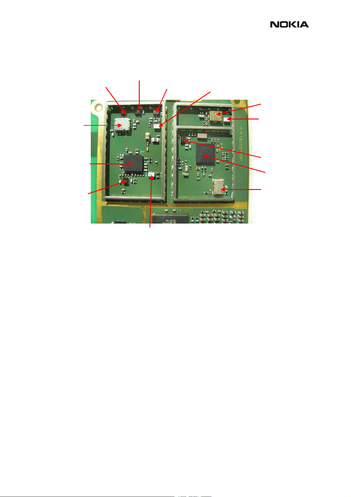
RF Key component placement
1900 RX SAW
900 RX SAW
CCS Technical Documentation
1900 LNA 1900 RX balun
4GHz VCO
Antenna
Switch Module
Power Amplifier
900 TX SAW
VCO balun
1800 RX SAW
Helgo86
RF ASIC
26 MHz VCTCXO
1800/1900 TX balun
Figure 1: Component placement 1
Issue 1 11/2004 COMPANY CONFIDENTIAL 4
Copyright © 2004 Nokia. All Rights Reserved.
Page 7
CCS Technical Documentation
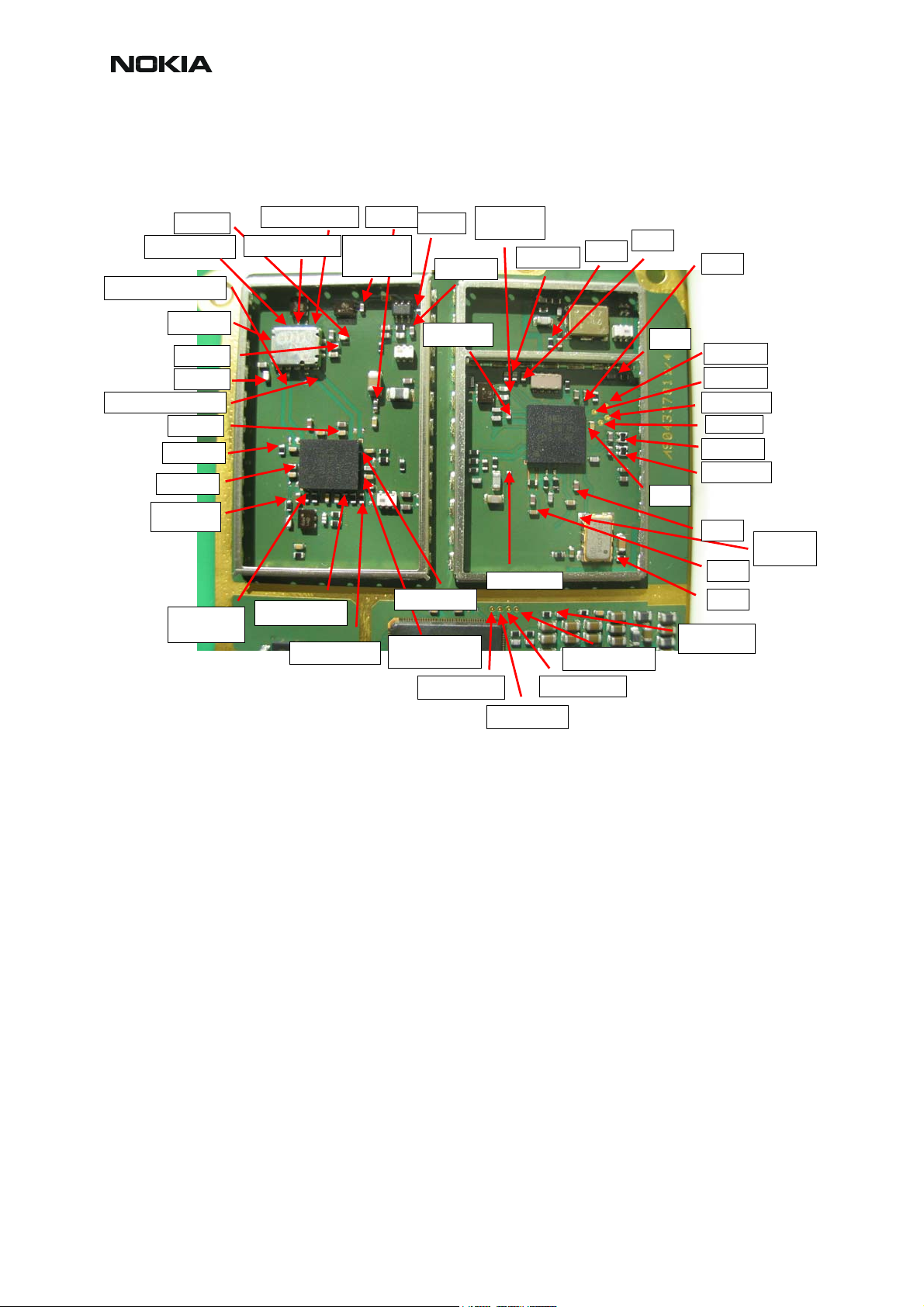
RF Measurement points
RM-12
VANT_3
ASM_in_900TX
To antenna
VANT_2
VANT_1
ASM_in_1800/1900TX
Mode
Iref_900
VTXB_900
PA_in_900
VPCTRL_900
ASM_out_1900RX
ASM_out_1800RXASM_out_900RX
VPCTRL_1800/1900
PA_in_1800/1900
VBAT
RX_1900_saw
_out
LNA_P
1900_RX_In
Iref_1800_1900
VTXB
_1800_1900
LNA_VCC
1800_RX_In
VPECTRL3(ALC)
900_RX_In
VR7
RFBusEna1/J7306
VR4
TXC
VR5
VR6
RXQ/J7303
RXI/J7302
TXP/J7300
TXA/J7301
TXQP/QN
TXIN/TXIP
VR1
VR2
VR3
26MHz to BB
VCTCXO
26Mhz out
RFBusReset/J7307 RFBusData/J7304
RFBusClk/J7305
Figure 2: Measurement points
5 COMPANY CONFIDENTIAL Issue 1 11/2004
Copyright © 2004 Nokia. All Rights Reserved.
Page 8

RM-12
CCS Technical Documentation
EGSM900, GSM1800 & GSM1900 Transmitter
General instructions for Tx troubleshooting
Kindly refer to the Service Software Section, Service Concept diagram.
Connect test jig to computer with DAU-9S cable or to FPS-8 Flash Prommer with XCS-4 mod-
ular cable.
Make sure that you have PKD-1 dongle connected to computer’s parallel port.
Connect DC power supply to module test jig with FLC-2 cable.
NOTE! When repairing or tuning transmitter use external DC supply with at least 3A current capability. Set the DC supply voltage to 4.2V.
Connect an RF-cable to the module test jig (MJ-32) RF connector and to measurement equipment or at least a 10dB attenuator, otherwise the PA may be damaged. Normally a spectrum
analyzer is used as measurement equipment.
NOTE! Normally Spectrum analyzer maximum input power is +30dBm. It is recommended to use
10dB attenuator on Spectrum analyzer input to prevent damage.
Set the phone module to test jig and start Phoenix service sofware.
Initialize connection to phone. (Use FBUS driver when using DAU9S, COMBOX driver when
using FPS-8.)
Select product from the menu:
File -> Choose product -> RM-12
From toolbar, set operating mode to "Local"
Activate RF controls window from the menu:
Testing -> RF Controls
From the RF controls window:
• Select band "GSM900" or "GSM 1800" or "GSM1900" (Default = "GSM900")
• Set Active unit to "Tx" (Default = "Rx")
• Set Operation mode to "Burst" (Default = "Burst")
• Set Tx data type to "Random" (Default = "All1")
• Set Rx/Tx channel to 37 on GSM900 band or 700 on GSM1800 band or 661 on
GSM1900 (Defaults)
• Set Tx PA mode to "Free" (Default)
• Set power level to 5 (Default = 19) on GSM900 or to 0 (Default = 15) on
GSM1800 or GSM1900
Issue 1 11/2004 COMPANY CONFIDENTIAL 6
Copyright © 2004 Nokia. All Rights Reserved.
Page 9
CCS Technical Documentation
g
g
p
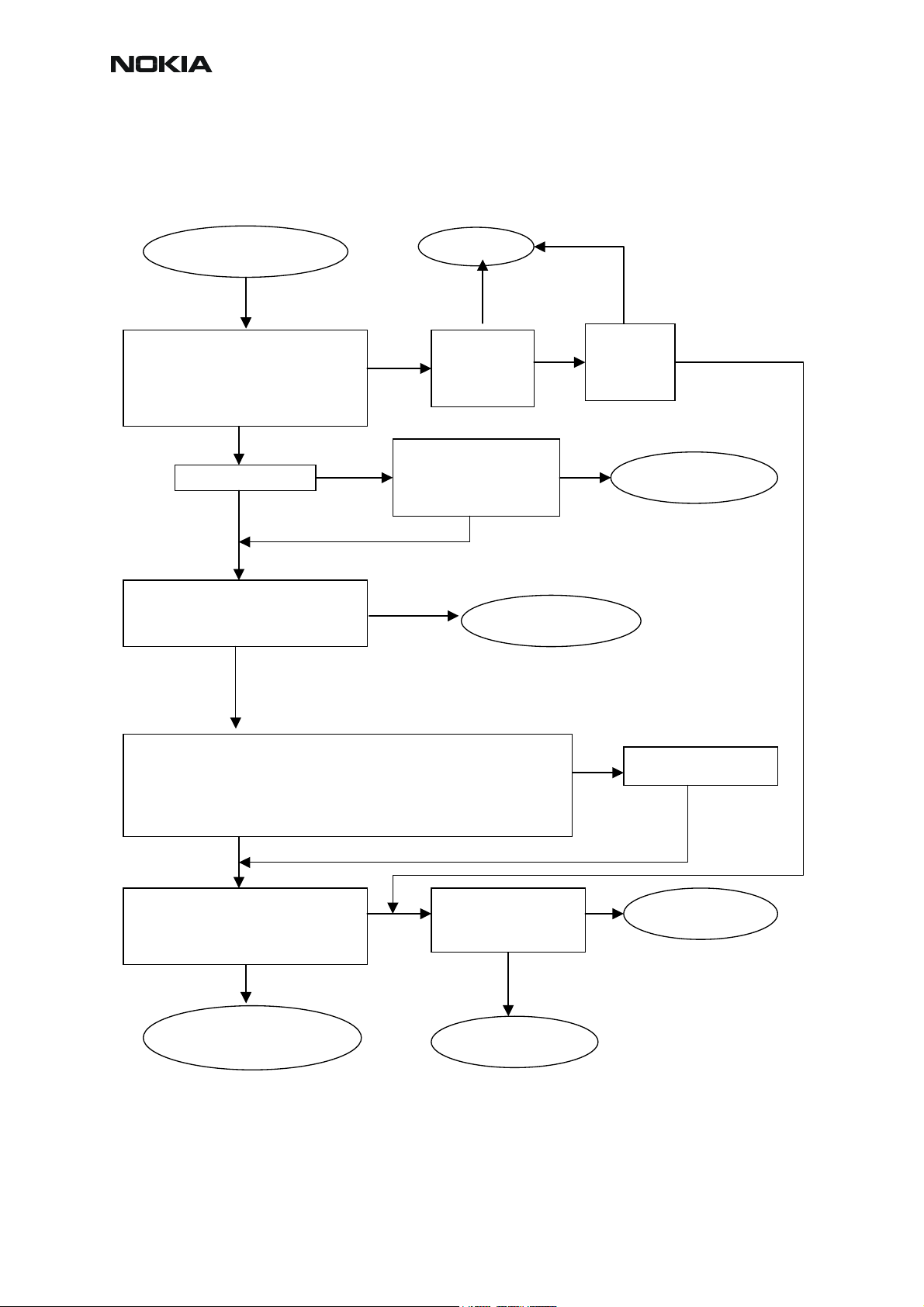
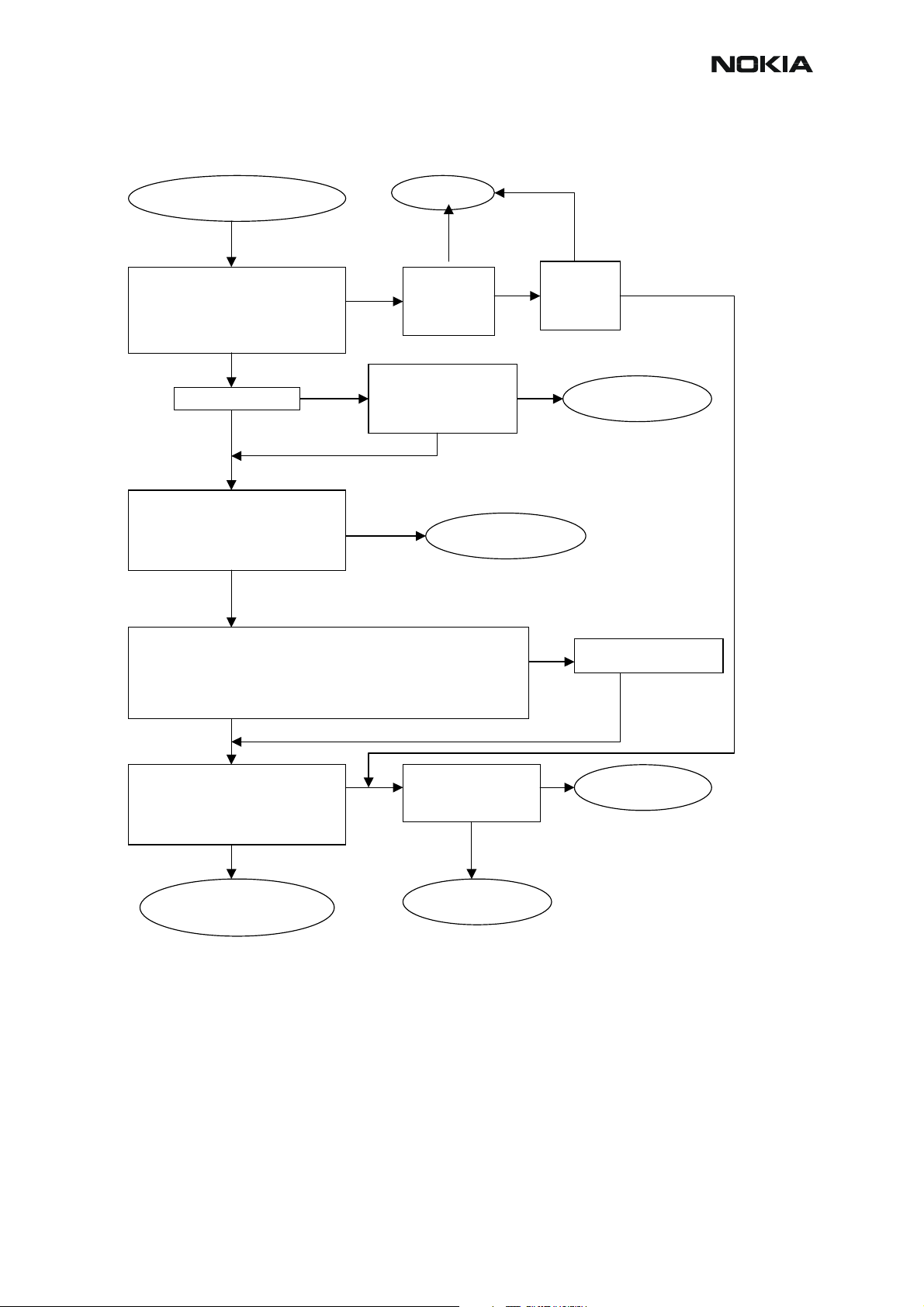
Transmitter troubleshooting diagrams
Yes
Yes No
Check output signal level:
+32…+33dBm@897.4MHz(GSM900)
+29…+30dBm@1747.8 and 1880MHz
(GSM1800&1900)
OK?
No
No Yes
Yes No
Check with RF probe signal level on
PA input: ~ -1…+5dBm
OK?
No
Yes
Start TX power level tuning and check tuned coefficient values:
Highest level ~0.655…0.831(GSM900); ~0.567…0.782(GSM1800&1900)
Yes
Lowest level ~0.166…0.196(GSM900); ~0.176…0 .225(GSM1800&1900)
Base level ~0.137…0.166(GSM900); ~0.132…0.161(GSM1800&1900)
Major differences?
No
Check control voltage with
Yes
oscilloscope:
PA Ctrl voltage >1.5V peak
No
OK?
Yes No
TX Troubleshooting
TX signal found?
PA & Antenna Switch
troubleshooting
Figure 3: Transmitter troubleshooting
TX OK
Check
all power
levels,
OK?
Check output signal
on 500MHz span
Signal found on incorrect
frequency?
Helgo
troubleshootin
Yes
Check control loop
components
OK?
Replace faulty
com
onents
Tune
TX power
levels,
OK?
Yes
No
Synthesizer
troubleshootin
Tune TX coefficient
values
Replace Helgo
RM-12
7 COMPANY CONFIDENTIAL Issue 1 11/2004
Copyright © 2004 Nokia. All Rights Reserved.
Page 10
RM-12
CCS Technical Documentation
Figure 4: HELGO IC troubleshooting
Check with oscilloscope:
-TXI/TXQ signals
No
-VR1, VR2, VR4, VR5, VR6 =2.8V
-VrefRF01 = 1.35V
-Helgo serial interface
-TXP & TXC signals
OK?
Yes
Check with RF probe:
4G VCO signal output:
No
-3589.6MHz (GSM900)
-3495.6MHz (GSM1800)
-3760MHz (GSM1900)
Level > - 10dBm
OK?
Yes
Yes
Check modulator output components
OK?
No
HELGO IC
troubleshooting
Replace faulty
component(s)
Baseband
troubleshooting
Synthesizer
troubleshooting
Replace HELGO
Issue 1 11/2004 COMPANY CONFIDENTIAL 8
Copyright © 2004 Nokia. All Rights Reserved.
Page 11
CCS Technical Documentation
p
)
p
RM-12
Check with RF probe signal level on PA
Yes Yes
input ~ -1…+5 dBm
OK?
Yes No
Check with oscilloscope:
-VBATT ~4V
-VTXB = 2.8V pulsed
-VPCTRL_900/1800/1900
OK?
Yes
Yes
PA & Antenna Switch
troubleshooting
No
Check component s
around PA
OK?
No
Replace faulty
onent(s)
com
Figure 5: PA and Antenna Switch troubleshooting
Check with oscilloscope:
-VANT1 (GSM900)
-VANT2 (GSM1800)
-VANT3 (GSM1900)
OK?
Check VANT line
components
OK?
Yes No
Replace faulty
onent(s
com
Replace PA
Replace
HELGO
Replace ant.
switch
9 COMPANY CONFIDENTIAL Issue 1 11/2004
Copyright © 2004 Nokia. All Rights Reserved.
Page 12
RM-12
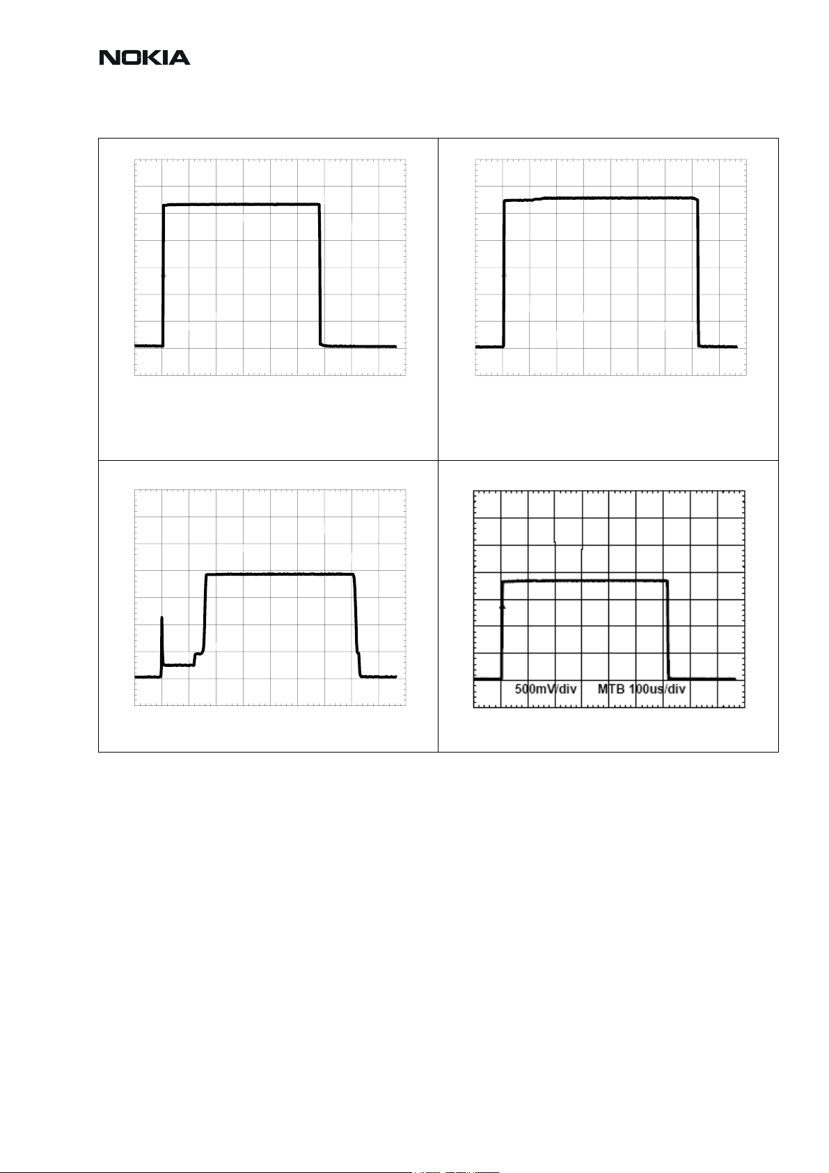
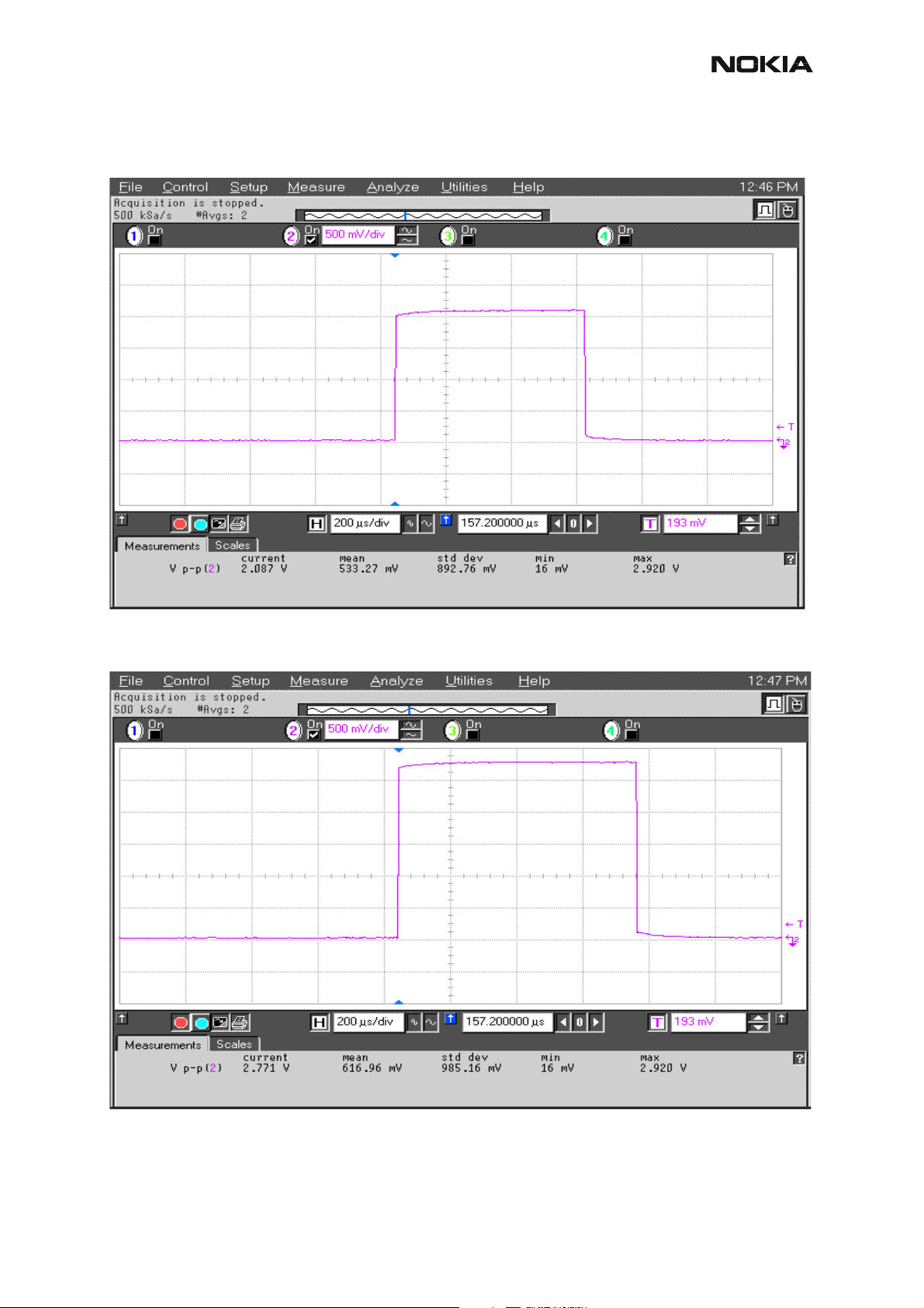
Pictures of transmitter signals
CCS Technical Documentation
Figure 6: Transmitter signals, VPCTRL
VPCTRL900 power level high at R7003
VPCTRL1800/1900 power level high at R7007
Figure 7: Transmitter signals
200mV/div
TX I/Q at R7304/7305 power level high Random data
100us/div
Issue 1 11/2004 COMPANY CONFIDENTIAL 10
Copyright © 2004 Nokia. All Rights Reserved.
Page 13
CCS Technical Documentation
RM-12
500mV/div 100us/div
VANT_1 / GSM900 TX at C7100
VANT_2 / GSM1800 TX at C7102
VANT_3 / GSM1900 TX at C7101 OV
(no signal/ Flatline on Oscilloscope screen)
500mV/div 100us/div
TXC at R7303
1
VTXB_900 at C7013
VTXB_1800_1900 at C7014
500mV/div 100us/div
TXP at J7300
11 COMPANY CONFIDENTIAL Issue 1 11/2004
Copyright © 2004 Nokia. All Rights Reserved.
Page 14
RM-12
m
A
CCS Technical Documentation
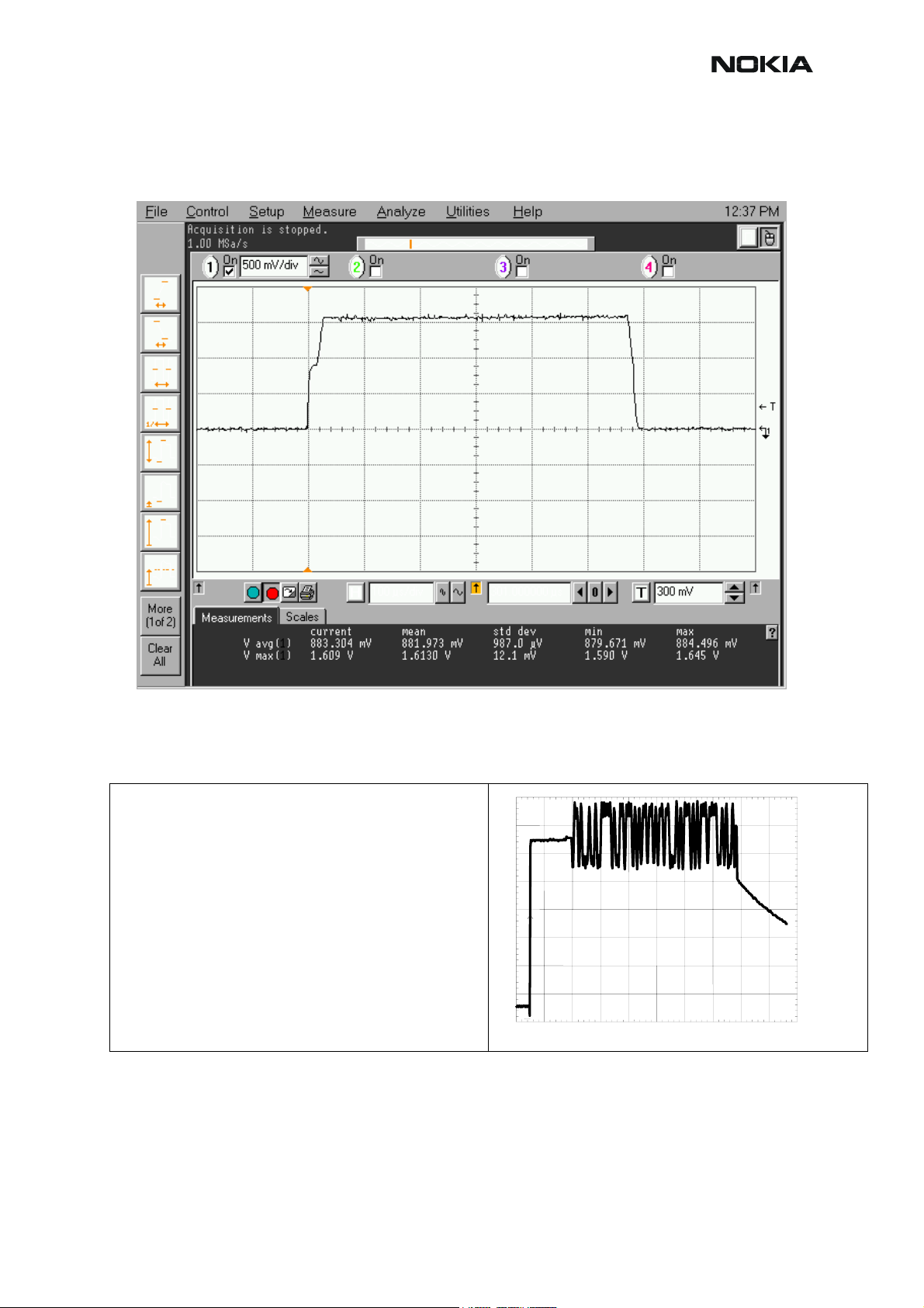
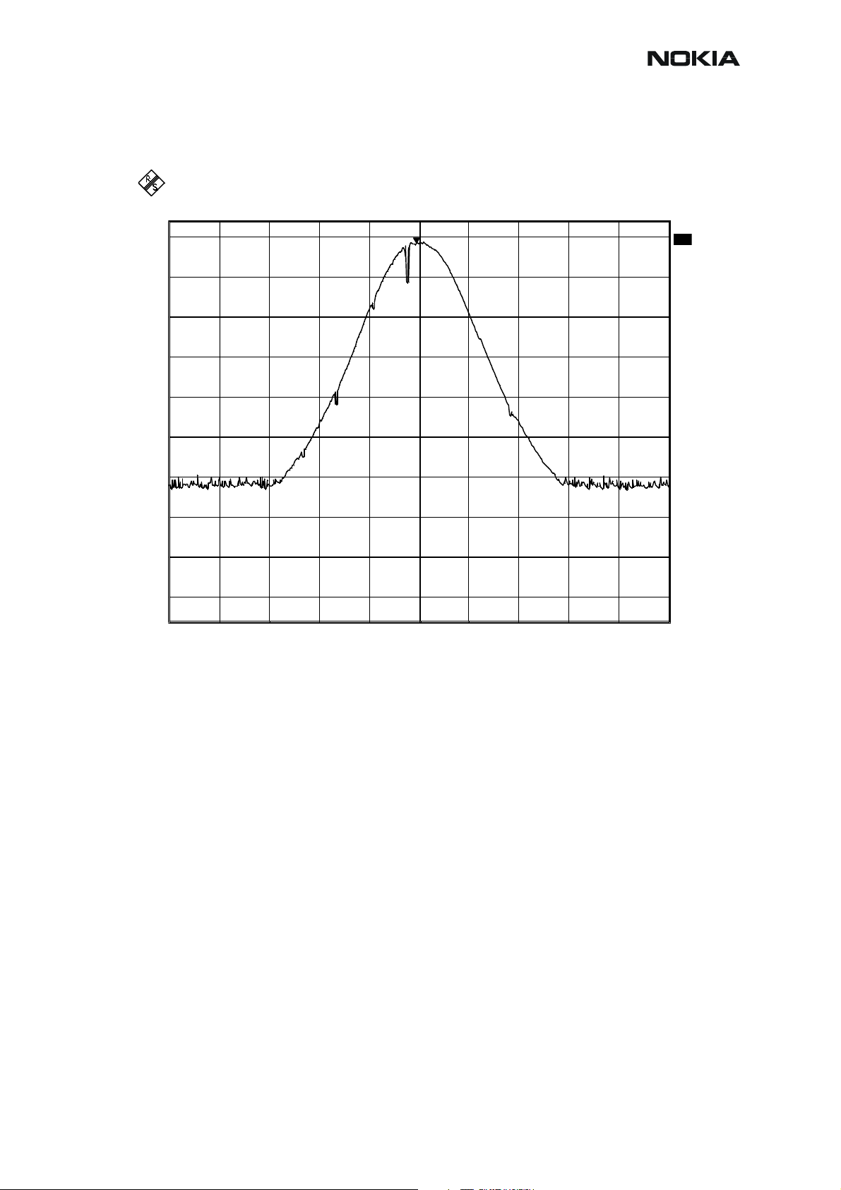
Figure 8: Tx out signal, 900 band, burst mode, channel 37
Ref Lvl
Ref Lvl
34 dBm
34 dBm
34
21 dB Offset
30
20
10
0
-10
-20
-30
-40
-50
Marker 1 [T1]
28.46 dBm
897.38997996 MHz
RBW 100 kHz
VBW 100 kHz
SWT 2 s
1
RF Att 40 dB
Unit dB
A
1M
-60
-66
Center 897.4 MHz Span 2 MHz200 kHz/
Date: 28.APR.2003 15:09:42
Additional information for EDGE troubleshooting
EDGE mode troubleshooting differs slightly from basic GSM troubleshooting
Establish connection to the phone normally (see GSM900/1800/1900 troubleshooting instructions).
Select product from the menu:
File -> Choose Product -> RM-12
From toolbar, set operating mode to “Local”
Activate RF controls window from the menu:
Testing -> RF Controls
From the RF controls window:
• Select Band “GSM900” or “GSM1800” or “GSM1900”
(Default=”GSM900”)
Issue 1 11/2004 COMPANY CONFIDENTIAL 12
Copyright © 2004 Nokia. All Rights Reserved.
Page 15

CCS Technical Documentation
• Set Active unit to “Tx” (Default=”Rx”)
• Set Edge “On” (Default=”Off”)
• Set Operation mode to “Burst” (Default=”Burst”)
• Set Tx data type to “Alternate PN9” (Default=”All1”)
• Set Rx/Tx channel to 37 on GSM900 or 700 on GSM1800 or 661 on
GSM1900 (Defaults)
• Set power level to 8 (Default = 19) on GSM900 or to 2 (Default = 15) on
GSM1800 or GSM1900
NOTE! For GSM900, Edge power levels 5, 6 and 7 are not in use, and for GSM1800&1900, Edge
power levels 0 and 1 are not in use.
RM-12
13 COMPANY CONFIDENTIAL Issue 1 11/2004
Copyright © 2004 Nokia. All Rights Reserved.
Page 16
RM-12
g
g
p
CCS Technical Documentation
Figure 9: Transmitter EDGE troubleshooting
TX EDGE Troubleshooting
Yes
Yes No
Check output signal level:
+24…+30dBm@897.4MHz(GSM900)
+22…+29dBm@1747.8 and 1880MHz
(GSM1800&1900)
OK?
No
No Yes
Yes No
No
Yes
Yes
No
Yes
No
Yes No
TX signal found?
Check with RF probe signal level on
PA input:
~-8dBm@PCL=8 (GSM900)
~-10dBm@PCL=2 (GSM1800&1900)
OK?
Start TX Edge power level tuning and check tuned coefficient values:
Highest level ~0.684…0.841(GSM900); ~0.763…0.860(GSM1800&190 0)
Lowest level ~0.333…0. 420(GSM900); ~0.323…0. 362(GSM1800&1900)
Base level ~0.273…0.313(GSM900); ~0.244…0.313(GSM1800&1900)
Major differences?
Check control voltages with
oscilloscope:
Pa Iref ~2V peak (GSM900)
Pa Iref ~2.1V peak (GSM1800@1900)
Mode ~1.8V OK?
PA & ant switch
EDGE troubleshooting
Yes
TX OK
Check
all power
levels,
OK?
Check output signal
on 500MHz span
Signal found on incorrect
frequency?
Helgo EDGE
troubleshootin
Check EDGE control
loop components
OK?
Replace faulty
com
onents
Yes
Tune
TX power
levels,
OK?
Synthesizer
troubleshootin
Tune TX coefficient
values
No
Replace Helgo
Issue 1 11/2004 COMPANY CONFIDENTIAL 14
Copyright © 2004 Nokia. All Rights Reserved.
Page 17
CCS Technical Documentation
Figure 10: Helgo EDGE troubleshooting
Check with oscilloscope:
-TXI/TXQ signals
No
-VR1, VR2, VR4, VR5, VR6 =2.8V
-VrefRF01 = 1.35V
-Helgo serial interface
-TXP & TXC & TXA
OK?
Yes
Check with RF probe:
4G VCO signal output:
No
-3589.6MHz (GSM900)
-3495.6MHz (GSM1800)
-3760MHz (GSM1900)
Level > - 10dBm
OK?
Yes
Yes
Check modulator output components
and VPECTRL3 signal
No
Helgo EDGE
troubleshooting
Replace faulty
component(s)
Baseband
troubleshooting
Synthesizer
troubleshooting
Replace HELGO
RM-12
15 COMPANY CONFIDENTIAL Issue 1 11/2004
Copyright © 2004 Nokia. All Rights Reserved.
Page 18
RM-12
p
)
p
)
CCS Technical Documentation
Figure 11: Pa & ant switch EDGE troubleshooting
PA & ant switch
EDGE troubleshooting
Check with RF probe signal level on PA
input:
~ -8dBm@PCL=8 (GSM900)
~ -10dBm@PCL=2 (GSM1800&1900)
OK?
Yes No
Check with oscilloscope:
-VBATT ~4V
-Iref _900 ~2V peak
-Iref_1800_1900 ~2.1V peak
-VTXB = 2.8V pulsed
-Mode = ~1.8V
OK?
No
Check components
around PA
OK?
Yes No
Yes
Replace PA
Yes Yes
Yes
Check with oscilloscope:
-VANT1 (GSM900)
-VANT2 (GSM1800)
-VANT3 (GSM1900)
OK?
Check VANT line
components
OK?
Replace
HELGO
Replace faulty
onent(s
com
Replace ant.
switch
No
Replace faulty
onent(s
com
Issue 1 11/2004 COMPANY CONFIDENTIAL 16
Copyright © 2004 Nokia. All Rights Reserved.
Page 19
CCS Technical Documentation
Pictures of EDGE transmitter signals
Figure 12: I_ref_900 power level 8 at R7019/C7001
RM-12
Figure 13: VTXB 900 power level 8 at C7013
17 COMPANY CONFIDENTIAL Issue 1 11/2004
Copyright © 2004 Nokia. All Rights Reserved.
Page 20
RM-12
CCS Technical Documentation
Figure 14: I_ref_1800/1900 power level 2 at R7017/C7000
Figure 15: VTXB 1800/1900 power level 2 at C7014
Issue 1 11/2004 COMPANY CONFIDENTIAL 18
Copyright © 2004 Nokia. All Rights Reserved.
Page 21
Figure 16: TXA 900/1800/1900 at C7309
Figure 17: TXI/TXQ signal at C7311/C7312/R7304/R7305
Page 22
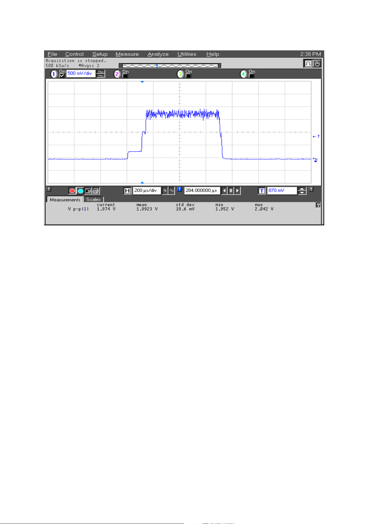
Figure 18: VPECTRL3 (ALC) signal at C7309
Page 23

RM-12
CCS Technical Documentation
EGSM900, GSM1800 and GSM1900 Receiver
General instructions for Rx troubleshooting
Connect test jig to computer with DAU-9S cable or to FPS-8 Flash Prommer with XCS-4 modular cable.
Make sure that you have PKD-1 dongle connected to the computer’s parallel port.
Connect DC power supply to module test jig with FLC-2 cable.
Set the DC supply voltage to 4.2V.
Connect an RF-cable to the module test jig (MJ-32) RF connector and to RF signal generator.
Set the phone module to test jig and start Phoenix service sofware.
Initialize connection to phone. (Use FBUS driver when using DAU-9S, COMBOX driver when
using FPS-8.)
Choose product from the menu:
File -> Choose product -> RM-12
From toolbar, set operating mode to "Local"
Activate RF controls window from the menu:
Testing -> RF Controls
From the RF controls window:
• Select band "GSM900", "GSM 1800" or “GSM1900” (Default =
"GSM900")
• Set Active unit to "Rx" (Default = "Rx")
• Set Operation mode to "Burst" (Default = "Burst")
For continuous mode:
• Set Operation mode to "Continuous"
• Set AGC to "12: FEG_ON + DTOS_ON + BB_30=Vgain60” (maximum
gain setting used in normal mode)
(Default = "14: FEG_ON + DTOS_ON + BB_42=Vgain72")
• Set Rx/Tx channel to 37 on GSM900 band, 700 on GSM1800 band or
661 on GSM1900 (Defaults)
Apply 942.46771 MHz (channel 37 + 67.710 kHz offset), 1842.86771 MHz (channel 700 +
67.710 kHz offset) or 1960.06771 MHz (channel 661 + 67.71 kHz) –90 dBm signal to the RFconnector (remember to compensate for cable attenuation).
Issue 1 11/2004 COMPANY CONFIDENTIAL 21
Copyright © 2004 Nokia. All Rights Reserved.
Page 24
RM-12
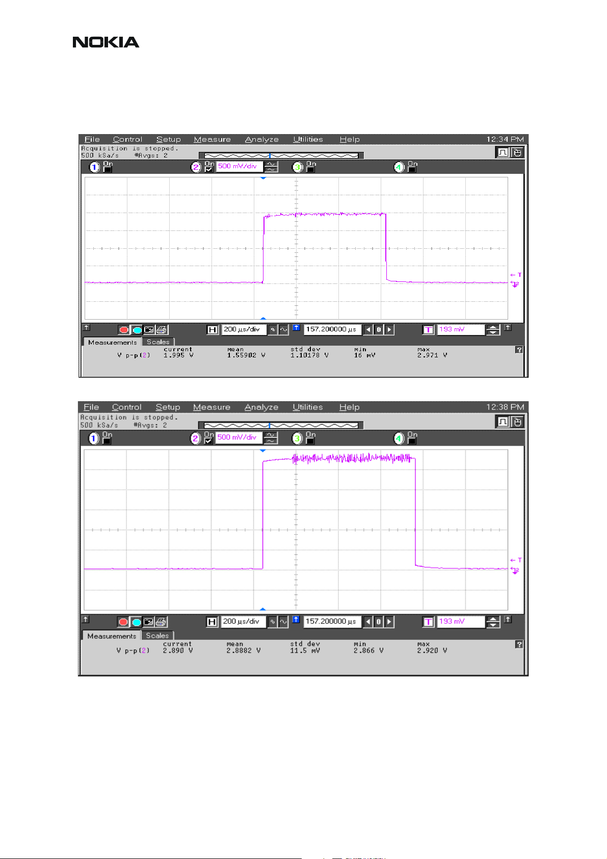
CCS Technical Documentation
Measuring with an oscilloscope on "RXI" or "RXQ" following screens should be seen on a working GSM900, GSM1800 or GSM1900 receiver:
Figure 1: RX I/Q signal, burst mode, input level –90dBm
Receiver I or Q burst mode signal (channel 37) measured from testpoint RXI or RXQ with
942.46771 MHz signal, input level –90dBm at RF-connector.
Correct signal amplitudes approximately:
• GSM900~170mVpp
• GSM1800~140mVpp
• GSM1900~160mVpp
Signal part frequency 67.7kHz sine.
DC level of signal part is 1.35V. DC level can variate about +/-100mV between I and Q signals
and between different bands as well.
22 COMPANY CONFIDENTIAL Issue 1 11/2004
Copyright © 2004 Nokia. All Rights Reserved.
Page 25
RM-12
CCS Technical Documentation
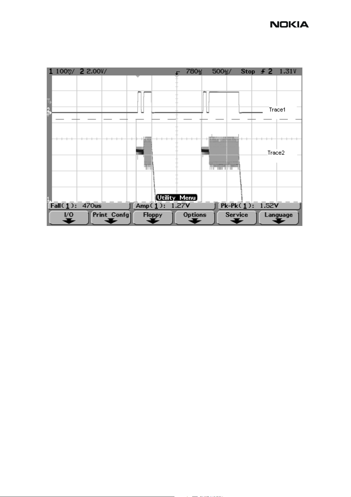
Figure 2: GSM1900 RX I or Q signal (trace2), burst mode
GSM1900 receiver burst mode I or Q signal at ch 661 with input signal 1960.067MHz, level –
90 dBm at RF-connector.
Trace2: With wider time scaling both monitoring and own RX bursts are seen, 1
nd
is monitoring and 2
burst (longer) is own RX burst.
st
burst (shorter)
Trace1: External LNA VCC supply voltage at burst mode, input level –90 dBm. Measured from
testpoint LNA_VCC.
Issue 1 11/2004 COMPANY CONFIDENTIAL 23
Copyright © 2004 Nokia. All Rights Reserved.
Page 26
CCS Technical Documentation
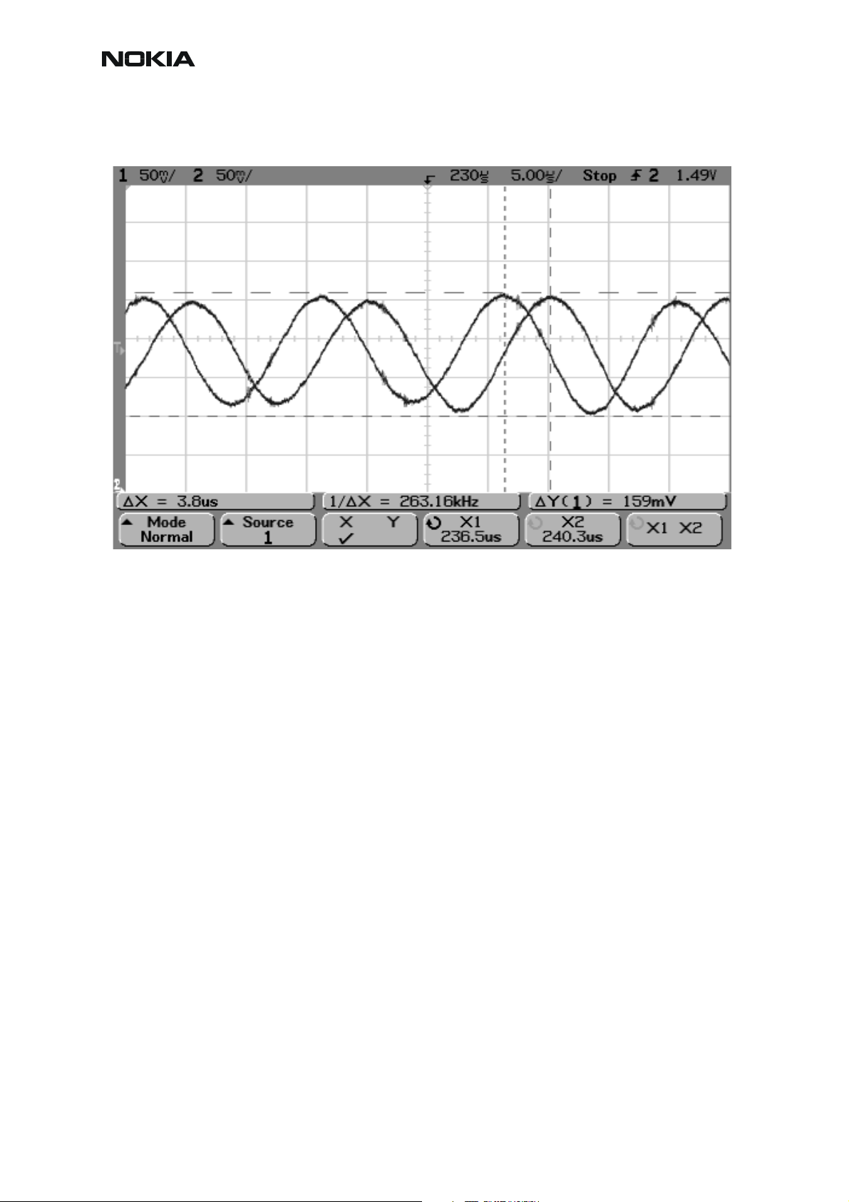
Figure 3: RX I&Q, phase difference 90 deg between signals
RM-12
Detailed view of GSM900 continuous mode RX I and Q signals measured from testpoints RXI
and RXQ simultaneously.
Used channel 37, input signal 942.46771 MHz, level –90 dBm at antenna port, AGC setting 12.
Phase difference should be 90 degrees between RX I and Q signals at all bands.
24 COMPANY CONFIDENTIAL Issue 1 11/2004
Copyright © 2004 Nokia. All Rights Reserved.
Page 27
RM-12
A
q
A
–
A
)
A
Troubleshooting diagram for GSM900 receiver
Phone in “Continuous” mode, AGC setting “12”..
CCS Technical Documentation
pply –90dBm
942.46771MHz signal
from generator to
antenna connector
Osilloscope at RX_I
signal 170mVpp DC
offset 1.35***
Fre
uency 67.7kHz
Rx 900 chain
functional
Check
L809,L810
L7104, L7103
Figure 4: GSM900 receiver troubleshooting
Note! Generator level can be set higher if
needed. Just note that levels will be different
in whole chain respectively.
Spectrumanalyzer:
ntenna Switch
output GSM900
88dBm
Spectrumanalyzer:
HELGO inputs
GSM900 –89dBm
Oscilloscope
VANT_1…3 0V
Check Antenna
Switch Z800
Spectrumanalyzer:
ntenna Switch
input –88dBm
Z7100
Oscilloscope:Check
HELGO serial
interface (burst
mode
Check
C809
X7100
Check
Baseband
Check SAW
Z809
Z7101
Check SAW
filter output
Oscilloscope:
VR1,3…6 2.7V
Check HELGO
serial interface
(burst mode)
Spectrumanalyzer:
4G VCO output
3769.6MHz
~-30dBm*
Check HELGO
N500
N7300
Check
Baseband
Synthesizer
troubleshooting
Check HELGO
N500
N7300
reading values are
measured with 1 kohm
passive probe (use
tweezers to connect the
probe ground to the nearest
PWB ground). Reading
value is represented without
+26 dB compensation.
* Spectrumanalyzer reading
with 1 kohm passive probe
(right value add +26dB)
*** DC-level of RXI/RXQ in
continuous mode will
decrase slowly. The original
level can be rest ored by
rewriting gain set
ll spectrumanalyzer
Issue 1 11/2004 COMPANY CONFIDENTIAL 25
Copyright © 2004 Nokia. All Rights Reserved.
Page 28
CCS Technical Documentation
A
q
A
A
)
A
Troubleshooting diagram for GSM1800 receiver
Phone in “Continuous” mode, AGC setting “12”.
RM-12
pply –90dBm
1842.86771MHz signal
from generator to
antenna connector
Osilloscope at RX_I
signal 170mVpp DC
offset 1.35***
Fre
uency 67.7kHz
Rx 1800 chain
functional
Z7102,
Check Z808,
L838,L839
L7105, L7106
Figure 5: GSM1800 receiver troubleshooting
Note! Generator level can be set higher if needed.
Spectrumanalyzer
ntenna Switch
output, GSM1800
-88dBm
Spectrumanalyzer
HELGO inputs
GSM1800 –88dBm
Just note that levels will be different in whole chain
respectively.
Spectrumanalyzer
input –84dBm
Oscilloscope
VANT_1…3 0V
Check Antenna
Z7100
Switch Z800
ntenna Switch
Oscilloscope:Check
HELGO serial
interface (burst
mode
Check
C809
X7100
Check
Baseband
Check Z808
Z7102
Check SAW
filter output
Oscilloscope
VR1,3…6 2.7V
Check HELGO
serial interface
(burst mode)
Spectrumanalyzer
4G VCO output
3685.6MHz
~-30dBm*
Check HELGO
N500
N7300
Check
Baseband
Synthesizer
troubleshooting
Check HELGO
N500
N7300
ll spectrumanalyzer
reading values are
measured with 1 kohm
passive probe (use
tweezers to connect the
probe ground to the nearest
PWB ground). Reading
value is represented without
+26 dB compensation.
* Spectrumanalyzer reading
with 1 kohm passive probe
(right value add +26dB)
*** DC-level of RXI/RXQ in
continuous mode will
decrase slowly. The original
level can be restored by
rewriting gain set
26 COMPANY CONFIDENTIAL Issue 1 11/2004
Copyright © 2004 Nokia. All Rights Reserved.
Page 29
RM-12
A
q
A
p
A
)
A
Troubleshooting diagram for GSM1900 receiver
Phone in “Continuous” mode, AGC setting “12”.
Figure 6: GSM1900 receiver troubleshooting
pply –90dBm
1960.06771MHz signal
from generator to
antenna connector
Note! Generator level can be set higher
if needed. Just note that levels will be
different in whole chain respectively.
CCS Technical Documentation
Osilloscope at RX_I
signal 160mVpp DC
offset 1.35***
uency 67.7kHz
Fre
Rx 1900 chain
functional
Spectrumanalyzer:
HELGO inputs
GSM1900 –88dBm
Check LNA
output from C829
–84dBm
Check Balun
T701 output
Z7104
C808, C807
C7111, C7112
C7110
Spectrumanalyzer:
ntenna Switch
outputs, GSM1900
ut -88dBm
SAW in
Oscilloscope:
VANT_3 2.7V
VANT_1/2 0V
Spectrumanalyzer:
RX_SAW_out –
90dBm (C826)
(C7108)
Oscilloscope:
LNA_VCC 2.6
LNA_P 0V
Check Antenna
Switch Z800
Z7100
Spectrumanalyzer:
ntenna Switch
input –84dBm
Oscilloscope:Check
HELGO serial
interface (burst
mode
Check Z806
Oscilloscope:
Check R800,
R7100
R810, L800
R7101, L7107
VR1,3…6 2.7V
Check HELGO
serial interface
(burst mode)
Z7103
Check
C809
X7100
Check
Baseband
Check HELGO
N500
N7300
Check Baseband
Oscilloscope:
VR1,3…6 2.7V
Check HELGO
serial interface
(burst mode)
Spectrumanalyzer:
4G VCO output
3920 MHz
~-30dBm*
Check HELGO
N500
N7300
Check
Balun
Check
Baseband
Synthesizer
troubleshooting
C7111,
Check C808,
L805, C807
L7108, C7112
Check
HELGO N500
N7300
ll spectrumanalyzer
reading values are
measured with 1 kohm
passive probe (use
tweezers to connect the
probe ground to the nearest
PWB ground). Reading
value is represented without
+26 dB compensation.
* Spectrumanalyzer reading
with 1 kohm passive probe
(right value add +26dB)
*** DC-level of RXI/RXQ in
continuous mode will
decrase slowly. The original
level can be restored by
rewriting gain set
Issue 1 11/2004 COMPANY CONFIDENTIAL 27
Copyright © 2004 Nokia. All Rights Reserved.
Page 30

RM-12
CCS Technical Documentation
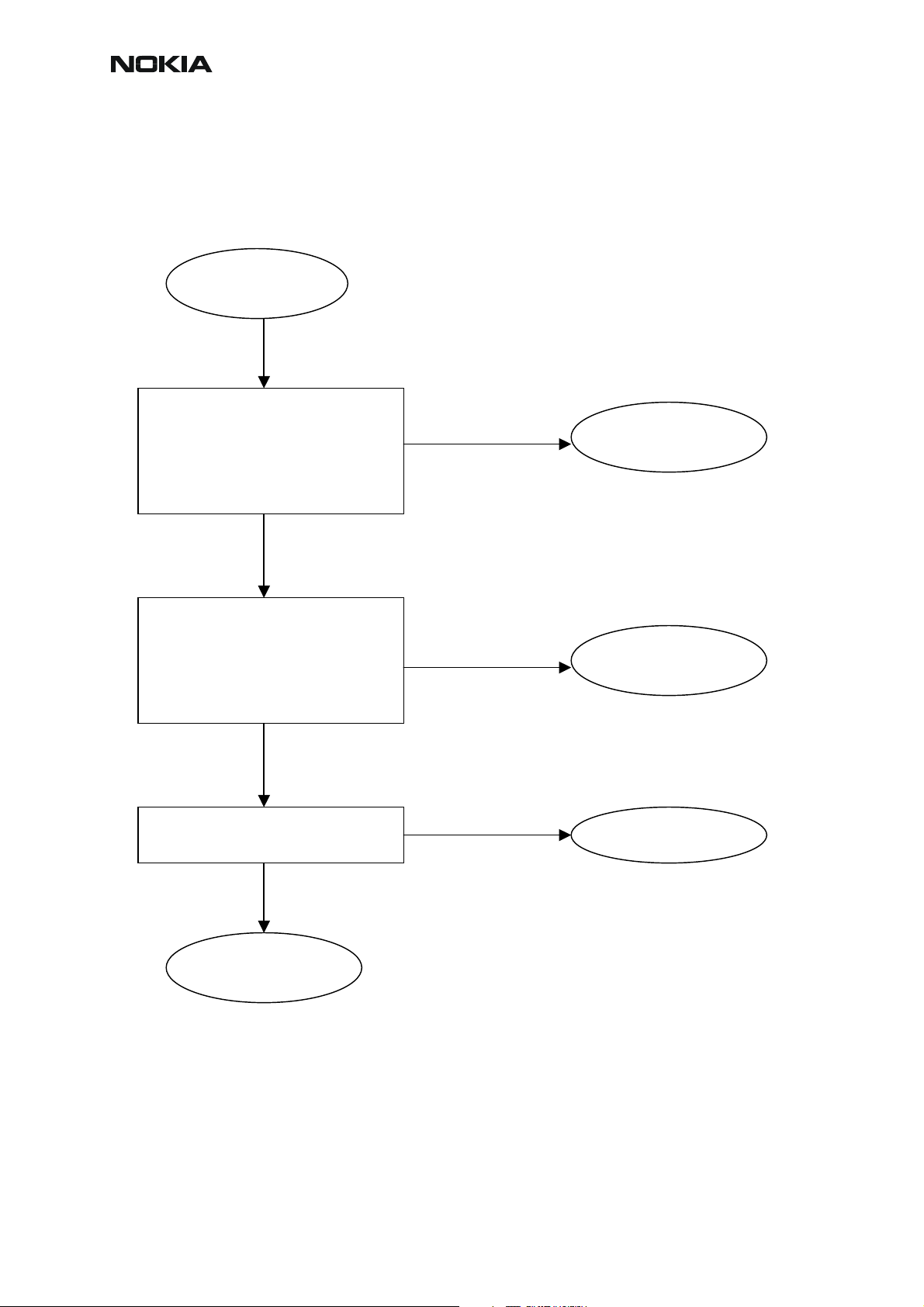
Synthesizer
General instructions for synthesizer troubleshooting
Connect test jig to computer with DAU9S cable or to FPS-8 Flash Prommer with XCS-4 modular cable.
Make sure that you have PKD-1 dongle connected to the computer’s parallel port.
Connect DC power supply or FPS-8 to module test jig with PCS-1 cable.
Set the DC supply voltage to 4.2V.
Set the phone module to test jig and start Phoenix service sofware.
Initialize connection to phone. (Use FBUS driver when using DAU9S, COMBOX driver when
using FPS-8.)
Select product from the menu:
File -> Choose product -> RM-12
From toolbar, set operating mode to "Local"
Activate RF controls window from the menu:
Testing -> RF Controls
From the RF controls window:
• Select band "GSM900", "GSM 1800" or "GSM1900" (Default =
"GSM900")
• Set Active unit to "Rx" (Default = "Rx")
• Set Operation mode to "Continuous" (Default = "Burst")
• Set Rx/Tx channel to 37 on GSM900 band, 700 on GSM1800 band, 661
on GSM1900 band (Defaults)
28 COMPANY CONFIDENTIAL Issue 1 11/2004
Copyright © 2004 Nokia. All Rights Reserved.
Page 31

RM-12
Synthesizer
troubleshooting
Yes
CCS Technical Documentation
Figure 7: Synthesizer troubleshooting diagram
*(When 2.5kOhm passive probe is used,
correct the measurement by +34 dB
Set with RF controls:
Active Unti = Rx
Operation mode = Continuous
Check with RF probe:
-4G VCO out signal
- 3589.6 MHz (GSM900)
-3495.6 MHz (GSM1800)
- 3760 MHz (GSM1900)
Level >-10dBm (*
OK ?
No
VCO out signal level<-10dBm
No
Check output signal on
1 GHz span
Signal found on
incorrect frequency ?
Yes
Yes
Synthesizer
OK
Yes
Check with oscilloscope:
-4G VCO Vcc = 2.7V
No
Check balun
output levels and
solder joints
OK ?
No
Replace
faulty
component(s)
OK ?
No
Yes
Yes
Baseband
troubleshooting
Replace
VCO
Check with oscilloscope:
VCO control voltage
from VCO pin
0V ?
No
Check with oscilloscope:
VCO control voltage
from VCO pin
>4.0 V ?
Yes
Check balun
output levels and
solder joints
OK ?
Yes
Check VCO control
loop components
Yes
OK ?
Replace
VCO
No
Replace
faulty
component(s)
No
Issue 1 11/2004 COMPANY CONFIDENTIAL 29
Copyright © 2004 Nokia. All Rights Reserved.
Page 32

CCS Technical Documentation
Pictures of synthesizer signals
Figure 8: 26MHz at G7200 pin out
RM-12
Figure 9: 26MHz RFCLK at R2902/C2902
30 COMPANY CONFIDENTIAL Issue 1 11/2004
Copyright © 2004 Nokia. All Rights Reserved.
Page 33

RM-12
CCS Technical Documentation
Figure 10: 1800 TX, channel 512, burst mode
Figure 11: 1900 RX, channel 810, continuous mode
Issue 1 11/2004 COMPANY CONFIDENTIAL 31
Copyright © 2004 Nokia. All Rights Reserved.
Page 34

CCS Technical Documentation
g
Figure 12: VCO output, 1800 band, ch700, RX on, continuous output
RM-12
RF test points
Signal Test Point Parameter Characteristics Note Function
TXP J7300 "1" and "0" 1.8/0 V digital signal Power amplifier enable
TXA J7301 "1" and "0" 1.8/0V digital signal Power control loop enable
RXI/RXQ J7302/J7303 voltage swing (static) 1.4Vpp DC level 1.4V Received demodulated I -and Q sign als
RFBus Data J7304 "1" and "0" 1.8/0V digital signal data frequency max. 10MHz RFBUs data; read/write
RFBusClk J7305 "1" and "0" 1.8/0V digital signal data frequency max. 10MHz RF Bus clock
RFBus Ena1 J7306 "1" and "0" 1.8/0V digital signal RFBus enable
RESET J7307 "1" and "0" 1.8/0V digital signal Reset to Helgo
RF GSM component alignment
Helgo (N7300) YES YES YES YES YES YES
PA (N700) NO NO NO NO YES YES
ASM (Z7100) NO YES YES YES YES YES
VCO (G7201) NO NO NO NO YES NO
TX SAW (Z7000) NO NO NO NO NO NO
RX LNA (V7100) NO YES YES NO NO NO
RX SAW (Z7101,Z7102,Z7103) NO YES YES NO NO NO
32 COMPANY CONFIDENTIAL Issue 1 11/2004
RX Channel Select Filter CalRX Cal RX Band Filter Response Cal RX DtoS Balance Cal TX IQ Tuning TX Power Level Tunin
Copyright © 2004 Nokia. All Rights Reserved.
Page 35

RM-12
Nokia Customer Care
Baseband troubleshooting
Partially damaged device
If the device is working, but some functionality is missing, try to localise the problem(s) and see
a relevant part of this manual. For example, if audio is not working see “Audio Troubleshooting”,
if charging is not working see “Charging troubleshooting”, and so on.
Most common symptoms reported by customer
Here you can find some common symptoms reported by customers when the device is brought
in for service. Some tips for locating the problem are also given. When troubleshooting, use
these tips and follow the given troubleshooting path.
Most common symptoms for audio problems
• “Earpiece sound is missing”
• ”Handsfree sound is missing”
• ”Microphone is not working”
• ”Ringing tones do not work”
• ”Audio volume too low”
• “IHF does not work”
If the symptom is one of the above, see “Audio troubleshooting”.
Most common symptoms for Bluetooth problems
• ”Bluetooth does not work or connection cannot be established”
Follow “Bluetooth troubleshooting” guidelines.
Symptoms related to energy management
• “Phone does not stay on”
• ”Charging is not working”
• ”Time is lost during battery change”
• ”Charging takes too long”
• ”Operating time is very short”
With these symptoms, follow “Power troubleshooting”.
Issue 1 11/2004 COMPANY CONFIDENTIAL 33
Copyright © 2004 Nokia. All Rights Reserved.
Page 36

CCS Technical Documentation
Problems related to UI-module
• “Touch Screen is not working”
• “Touch Screen is working unreliably”
• “Keypad is not working”
• ”Rocker is not working”
• ”Backlight is dim”
• ”Backlight not even”
• ”Backlight is blinking”
• ”Keypad or display backlight is not working”
RM-12
• ”Display-related problems”
See “UI troubleshooting”.
Most common RF-related symptoms
• “Call cannot be made”
• ”Phone does not find signal”
• ”Call is often dropped”
See “RF troubleshooting”.
Problems related to camera
• “Bad image quality”
• ”Picture cannot be taken”
See “Camera module troubleshooting”.
34 COMPANY CONFIDENTIAL Issue 1 11/2004
Copyright © 2004 Nokia. All Rights Reserved.
Page 37

RM-12
Dead or jammed device troubleshooting
Dead phone
Place service
battery via
ammeter=
Power On
Nokia Customer Care
Yes
Any image on
screen
Yes
Normal
operation
No No
No
Ammeter
>> 0 mA
Yes
Connect PC to
Phone using DAU-
9S cable.
Scan product
RM-12
found
Yes
Normal
operation
No
Flash the phone Succeed
Go to/visit display
No
troubleshooting
Normal
operation
No
No
Go to power
troubleshooting
Go to OMAP1510
troubleshooting
Yes
Yes
Yes
End test
Issue 1 11/2004 COMPANY CONFIDENTIAL 35
Copyright © 2004 Nokia. All Rights Reserved.
Page 38

CCS Technical Documentation
OMAP1510 (1)
Start
Booting
problems?
Yes
Visit APE Power
troubleshooting
APE Power
OK/fixed,
problem
solved?
No
Check resistor
R4806, replace
if needed.
Problem
solved?
RM-12
Yes
Yes End
No
No
Visit APE clock
troubleshooting
Vis it SDRAM
troubleshooting
Was it a
SDRAM
problem?
No
Yes
APE clocks/
reset OK/fixed,
problem
solved?
No
Go to /(visit) APE
NAND
troubleshooting
Was it a NAND
problem?
Yes
End
Yes
End
No
Replace
engine board.
OMAP1510 D4800
36 COMPANY CONFIDENTIAL Issue 1 11/2004
Copyright © 2004 Nokia. All Rights Reserved.
Page 39

RM-12
SDRAM (1)
Start
Run
ST_APE_RAM_
TEST, with
Phoenix.
Result?
All signals in this
troubleshooting are in
range 0 - V18
Problem
Pass
occurs only in
heat or cold?
No
Use cold spray/
hot air to SDRAM device
or customer feedback
Phone might been
dropped, solder
Yes
balls cracked,
replace D5080
Nokia Customer Care
Fail
Measure
SDRAM
voltage V18 at
C5083
Correct
Measure SDCLK
Measure
SDCLK
frequency at
frequency at
R4808 = 75MHz,
R4808
(1.8V).
>70MHz?, level
0 - ~V18
No
Go to SDRAM
troubleshooting
page 2
Incorrect
Yes
Go to OMAP1510
troubleshooting
Check and replace
if needed C5083-
Check C5083 - C5089.
C5089, res ist ance
>>1Mohm
Correct
Phone might been
dropped, solder
balls cracked,
replace D5080
Measure
SDRAM
voltages V18
at C5083
Incorrect
Correct
Visit APE Power
troubleshooting
Measure
SDRAM
voltages V18
at C5083
Incorrect
Change SDRAM
D5080
Issue 1 11/2004 COMPANY CONFIDENTIAL 37
Copyright © 2004 Nokia. All Rights Reserved.
Page 40

CCS Technical Documentation
SDRAM (2)
From SDRAM
troubleshooting
page 1
Replace
Inspect R4808
value, approx
22ohm
No
R4808 and
measure
SDCLK
frequency
>>70Mhz
Yes
Rerun
ST_APE_RAM_
TEST with
Phoenix
Fail
Change SDRAM
D5080
RM-12
Yes
No
Problem
occurs while
booting?
Yes
Go to Seija/NAND
troubleshooting
Pass
No
Go to OMAP1510
troubleshooting
38 COMPANY CONFIDENTIAL Issue 1 11/2004
Copyright © 2004 Nokia. All Rights Reserved.
Page 41

RM-12
APE flash
Nokia Customer Care
All signals in this
troubleshooting are in
range 0 - V18
Busy# signal rises
at latest after
1055us after
RSTIN# rises.
However, the Busy#
can be high before
RSTIN# rises, but this
is not taken into account.
Start
Measure
MDOC Busy#
at R4801 and
RSTIN# at
J4803
RSTIN# stays low
Measure
MPU_nReset at
R4802, low to
high transition?
Stays low
Yes
Backup user data before
MDOC troubleshooting, if
Boot phone.
Use oscilloscope.
Busy#
stays low
Go to OMAP1510
troubleshooting
possible
Check resistor
R4801
~10k
Yes
Check MDOC
core voltage at
C5000, V28
Correct
voltages
No
Replace resistor
R4801 and rerun
first test
Voltage levels
invalid
Check
resistors
R5000 and
R5001,
both ~10k
Yes
Measure
CS0# at J4805
and OE#
J4802,
toggling?
Yes
Memory
corrupted, reflash,
or replace MDOC
D5000
Replace damaged
No
Go to OMAP1510
No
Go to APE reset
troubleshooting
resistor(s)
troubleshooting
Check MDOC
I/O voltage at
C5001,
V18
Correct
voltages
Check
resistors
R5000 and
R5001,
both ~10k
Yes
MDOC damaged,
replace D5000
Voltage
level
invalid
No
Go to APE Power
troubleshooting
Replace damaged
resistor(s)
Issue 1 11/2004 COMPANY CONFIDENTIAL 39
Copyright © 2004 Nokia. All Rights Reserved.
Page 42

RM-12
CCS Technical Documentation
ASIC is changed
ASICs can be changed only at a defined service level.
• If UEM is changed
If UEM is changed, baseband calibrations should be made. IMEI must be prog rammed also.
• If UPP8M is changed
If UPP is changed, there is no need to flash the phone.
• If Zocus is changed
If Zocus is changed, it must be calibrated.
• Nor flash changed
If CMT Nor flash is changed, re-flash the phone. IMEI must be programmed also.
• SDRAM changed
If SDRAM is changed, there is no need to flash the phone.
• MDOC flash changed
If MDOC memory is changed, User data needs to be back-upped if possible. Re-flash the
phone.
• Touch screen controller
If touch screen controller or display module is changed, calibrations should be made.
•BT
If BT chip is changed, there is no need to flash the phone.
Test points
Test point locations and possible signal levels are listed in the Schematics chapter of this Service Manual.
Selftests / “Contact service” on display
MCU selftest cases can be split into two categories: ones that are executed during power up
and ones that are executed only with a PC connected.
“CONTACT SERVICE” on display means that software is able to run and thus the watchdog of
UEM can be served. Selftest functions are executed when the phone is powered on a nd if one
or more selftest functions fail, the message “Contact Service” is shown on the display.
40 COMPANY CONFIDENTIAL Issue 1 11/2004
Copyright © 2004 Nokia. All Rights Reserved.
Page 43

RM-12
Nokia Customer Care
PC selftests are listed below:
Table 1: PC selftests
Test Description
ST_AUX_DA_LOOP_TEST This function tests the connection of
AuxDa and UemInt signals between
UPP and UEM.
ST_EAR_DATA_LOOP_TEST This function tests the connection of
EarData and MicData signals between
UPP and UEM.
ST_KEYBOARD_STUCK_TEST This function tests if some key is
stucked.
ST_MBUS_RX_TX_LOOP_TEST
ST_SIM_CLK_LOOP_TEST
ST_SIM_IO_CTRL_LOOP_TEST
ST_SLEEP_X_LOOP_TEST
ST_TX_IDP_LOOP_TEST
This function tests the connection of
MBusTx and MBusRx signals between
UPP and UEM.
This function tests the connection of
SimClk and SimIODa signals between
UPP and UEM. This test requires also
that SimIOCtrl signal can be set to high
state.
This function tests the connection of
SimIOCtrl and SimIODa signals
between UPP and UEM. This test
requires also that SimClk signal can be
switched.
This function tests the connection of
SleepX and SleepClk signals between
UPP and UEM.
This function tests the connection of
TxIdp and RxIdp signals between UPP
and UEM.
ST_TX_IQ_DP_LOOP_TEST
This function tests the connection of
TxQdp and RxQdp signals between
UPP and UEM.
ST_BACKUP_BATT_TEST
This function tests if the backup battery
was ok during power-up.
ST_LPRF_IF_TEST
This test verifies, whether BT MCM
internal selftests are o.k.
Issue 1 11/2004 COMPANY CONFIDENTIAL 41
Copyright © 2004 Nokia. All Rights Reserved.
Page 44

CCS Technical Documentation
RM-12
Table 1: PC selftests
ST_CAMERA_IF_TEST
Purpose of this test is to verify the cam-
era data and I2C lines. I2C interface test
and camera activation is done first and
then camera sends test picture to the
OMAP.
ST_WARRANTY_TEST
This function tests the Warranty Infor-
mation State.
ST_FLASH_CHECKSUM_TEST
This test computes the checksums over
flash ROM areas and compares them to
the pre-calculated checksums in flash
header.
ST_RADIO_TEST
Purpose of this test is to check that radio
data line is working properly.
ST_LPRF_AUDIO_LINES_TEST
This test verifies the LPRF audio lines.
ST_UEM_CBUS_IF_TEST This test verifies the CBUS connection
of CBUSCLK, CBUSDA, and CBUSENX
signals between UPP and UEM.
ST_VIBRA_TEST This test verifies the vibra lines.
ST_SLEEPCLK_FREQ_TEST Purpose of this test is to check the basic
functionality of
ST_SLEEPCLK_FREQ_TEST.
ST_CURRENT_GAUGE_IF_TEST Purpose of this test is to check that
ST_CURRENT_GAUGE_IF_TEST is
working in real HW environment. Test
uses current gauge registers to verify,
that correct HW-module is in place and
working properly.
ST_CMT_APE_WAKEUP_TEST Purpose of this test is to check that
ST_CMT_APE_WAKEUP_TEST is
working properly.
ST_MAIN_LCD_IF_TEST Purpose of this test is to check that dis-
play interface (OMAP and LCD) is work-
ing properly.
ST_TOUCH_STUCK_TEST Purpose of this test is to check that
touch interface is working properly.
ST_APE_DAC_CTRL_IF_TEST Purpose of this test is to check connec-
tions (I2C lines) between APE and DAC.
Audio driver provides the test interface.
42 COMPANY CONFIDENTIAL Issue 1 11/2004
Copyright © 2004 Nokia. All Rights Reserved.
Page 45

RM-12
Nokia Customer Care
Table 1: PC selftests
ST_APE_RAM_TEST Purpose of this test is to check that
ST_APE_RAM_TEST is working prop-
erly. Test starts RAM testing and loops
the result until response from APE boot-
code is received.
ST_APE_POST_CODE_TEST Purpose of this test is to check that
ST_APE_POST_CODE_TEST is (boot-
code) working properly.
ST_BT_WAKEUP_TEST Purpose of this test is to check that
UART interface from the OMAP to the
Bluetooth module. The Bluetooth ASIC
self-test runs automatically as part of the
boot-up sequence. It is based on the
assumption that UART communication
is required to successfully run the initiali-
sation sequence. It cannot be assumed
that if the connection works if a UART
command is sent to the Bluetooth ASIC.
Therefore, the Bluetooth ASIC must
send the status information (OK/Not OK)
to the test server in the boot sequence.
ST_XABUS_TEST Purpose of this test is to check that
ST_XABUS_TEST is working in real HW
environment. Test checks the communi-
cation bus between CDSP and Applica-
tion DSP and therefore this test cannot
be executed in MOSIM environment.
Also ST_FAIL situation would be too dif-
ficult to simulate comparing to benefits.
ST_PWR_KEY_TEST Purpose of this test is to check that pwr
key is working properly.
Issue 1 11/2004 COMPANY CONFIDENTIAL 43
Copyright © 2004 Nokia. All Rights Reserved.
Page 46

CCS Technical Documentation
Flashing troubleshooting
Flashing does
not work
Check cables and
flashing adapter. Verify
that you have the right
data package
From APE flashing
troubleshooting
RM-12
From the CMT
flashing
troubleshooting
OK? No
Go to CMT
flashing
troubleshooting
RM-12
Check Nokia 7710
flashing
instructions
44 COMPANY CONFIDENTIAL Issue 1 11/2004
Copyright © 2004 Nokia. All Rights Reserved.
Page 47

RM-12
APE Flashing
From the CMT
flashing
troubleshooting
Flashing
stalls. "ADL ->
sending code: x%"
(x<100) ?
No
Yes
Nokia Customer Care
Go to NAND
troubleshooting
Run
ST_APE_POST_
CODE_TEST with
Phoenix
pass
Go to USB
troubleshooting
Reflash
Fail
Phone starts
to boot, but jams
after a while ?
No, totally dead device
Go to APE power
troubleshooting
Yes
CMT functionality
OK and automatically
ran self tests passed?
Yes
Go to OMAP1510
troubleshooting
No
Go to CMT
troubleshooting
Issue 1 11/2004 COMPANY CONFIDENTIAL 45
Copyright © 2004 Nokia. All Rights Reserved.
Page 48

CCS Technical Documentation
CMT flashing
Note! OMAP, UEM and UPP are unchangeable.
From the top
level
Measure FBUS
and BSI signals
while flashing
FBUS TX is
HIGH during
flashing?
No
BSI pulse
exists during
flashing?
RM-12
Check BSI line
including X2020,
No
R2035, C2020,
R2201, C2225 and
R2202
Yes
IS FBUS TX set LOW
after it has been
HIGH
Yes
Check Phoenix
Prommer Tool
window
information
Wrong
Manufacturer
ID or
Device ID
No
Is FBUSTX
~1.8V during
flashing
Yes
No
Yes
No
Check R2025, if
OK change UEM
Change UPP
(D2800)
Change flash
(D3000)
Go to APE flashing
troubleshooting
Reflash
46 COMPANY CONFIDENTIAL Issue 1 11/2004
Copyright © 2004 Nokia. All Rights Reserved.
Page 49

RM-12
Power troubleshooting
Nokia Customer Care
Table 2: Power troubleshooting
Regulator
reference
Output
name
Output
voltage
Test point Supply to
N4201 V15 1.57 C4214 D4800 Omap1510 core
N4202 V18 1.8 C4212 D4800 Omap 1510 io, D5080
SDRAM, D5000, MDOC, camera
N4200 V28 2.8 C4202 D4800 Omap 1510 io, camera con-
verter, display module, N4400
touch controller
N5200 VMMC 3 C5202 MMC
N2000 Vout 2.8 C2000 Pop-port
N2001 V33 3.3 C2005 D4800 Omap 1510 USB
D4420 VLED 10..11V C4424 Backlight, keylight
Issue 1 11/2004 COMPANY CONFIDENTIAL 47
Copyright © 2004 Nokia. All Rights Reserved.
Page 50

CCS Technical Documentation
CMT
Note! OMAP, UPP and UEM are unchangeable.
NO power
up
Connect service
battery to phone
and measure
current when
powering on
RM-12
Current rises
over 100mA but
drops down
NO
Current short
NO
Current 0mA all
the time
NO
Disassemble
phone
Check CMT
voltages:
C2232=2.8V,
C2202=2.8V,
C2204=1.8V,
C2205=1.5V
All Voltages ok
w he n power
button pressed
YES
YES Flash phone SW
NO
YES
Disassemble
phone and check
visually possible
shortcircuits and
YES
damaged or over
heated
components
Check Battery
YES
NO
connector
C2232=2.8V to
RF, C2202=2.8V
to R2201 and
N4201,
C2204=1.8V to
D2800 and D3000,
C2205=1.5V to
D2800
Current rises
over 100mA but
drops down
Any damaged
component found
and changed
Remowe RF VBAT
NO
NO
Change damaged
component on
voltage not in
spec.
YES
filter L7000
Perform EM
calibration with
Phoenix and
JBV-1
All Voltages ok
w he n power
button pressed
Current short Goto RF checkingNO
YES
Change R2036,
Current short
YES
CSP compone n t
on VBATT:
N2000, N2070,
N2100, N2200,
N4200, N4201,
N4202, N5200
Change UEM
NO
D2200
Check CMT Res e t
and clocks.
YES
48 COMPANY CONFIDENTIAL Issue 1 11/2004
Copyright © 2004 Nokia. All Rights Reserved.
Page 51

RM-12
Charging
Not
charging
Connect
service battery
and read BSI
by Phoenix
75kohm
100kohm
YES
Connect charger
and read Vchar
voltage by
Phoenix ACP-12
5.7V
NO
Note! OMAP, UEM and UPP are unchangeable.
Perform EM
calibration by
NO
NO
YES Flash phone SW
Phoenix and
JBV-1
Charging OK
Read BSI b y
Phoenix. With
servce battery
100kohm
75kohm
YES
YES
Flash phone SWNO
Read BSI b y
Phoenix. With
servce battery
75kohm
100kohm
YES
Change R2201
and R2202
Nokia Customer Care
Disassemble
NO
phone and check
Battery contacts .
R2202, Norma l
NO
Phone in jig.
Measure
voltage on
mode 1.3V
Perform EM
calibration by
Phoenix and
JBV-1
Connect charger
and read Vchar
voltage by
Phoenix ACP-12
5.7V
NO
Flash phone SW
Charging OK
NO
NO
Charging OKYES
Charging OK
Disassemble
phone and change
NO Charging OK
Measure Vchar
from fuse F2020
5.7V
YES
YES
R2200
NO
Measure Vchar
from fuse F2020
calibration by
Change fuse
F2020
5.7V
NO
Perform EM
Phoenix and
JBV-1
NO
NO
Change UEM
D2200
Charging OK
Disassemble
phone. Check
charger connector.
Measure Vchar
from L2020 5.7V
Change fuse
F2020 and V2020.
NO
YES
Change L2020
Issue 1 11/2004 COMPANY CONFIDENTIAL 49
Copyright © 2004 Nokia. All Rights Reserved.
Page 52

CCS Technical Documentation
APE
RM-12
Power on
Supply voltage
drops(or current
is large)?
NO
Measure VBAT
from input filters
C4200, C4209,
L4203(both sides)
OK?
YES
Check
V28(~2.8V),
OK?
YES
Visit APE reset
troubleshooting
YES
NO
NO
Note! OMAP, UEM and UPP are unchangeable.
Short circuit in
VBAT line
Failure on VBAT
line, check
components and
connectors
Check
enable(VIO),
high (1.8V)?
NO
UEM fault
YES
Change V28
regulator(N4200)
and retest, OK?
NO
Shortcut in V28
line
Check SYNC/
MODE fr o m
R4202 (both
sides), High
(>2V)?
YES
Check
V15(~1.57V),
OK?
YES
Check V18
(~1.8V), OK?
YES
END
R4200 or
Faulty V1600 or
NO
NO NO
R4202, change
and retest
V15 > 1.62V ?
V18 >1.89V ?NO
No
Check
enable (VIO),
high (1.8V)?
NO
UEM fault
YES
NO
Check enable
(VFLASH1),
high (2.8V)?
NO
UEM fault
Check
ref. voltage
at C4211,
1.35V ?
NO
Ref .
voltage found
at either end of
L4200 ?
YES
YES
YES
YES
Check
voltage at L4201
(both sides low),
~0V ?
Change coil and
retest V15
YES
Check
voltage at L4202
(both sides low),
<1V ?
Change filter
(L4200)
NO
YES
NO
Change coil and
retest V18
Change SMPS
chip(N4201) and
retest, OK?
Shortcut in V15
YES
NO
line
Change SMPS
chip (N4202)
and retest, OK?
NO
Shortcut in
V18 line
50 COMPANY CONFIDENTIAL Issue 1 11/2004
Copyright © 2004 Nokia. All Rights Reserved.
Page 53

RM-12
APE Clocking
APE clocks
trouble
shooting
Clk32k (J4815):
Voh ~ 2.8V &
f ~ 32.768kHz ?
(Figure 1)
Nokia Customer Care
Reflash the phone
SleepClk ( J2802):
No
Voh ~ 1.8V &
f ~ 32.768kHz ?
(Figure 2)
first and check that
Clk32k is not shorted
to GND or some
Yes
power line. If Clk32k
still doesn't w ork,
change UEM
Yes
12Mhz clock
(C4800, OSC1_IN):
Vpp ~ 1.7V &
f ~ 12.0MHz ?
(Figure 3)
Yes
Check that
(C4800, OSC1_IN)
DC-offset ~ 720mV
(C4802, OSC1_OUT)
DC-offset ~760mV
(Figures 3&4)
Yes
Solder joints of
C4800, C4801,
C4802 and B4800
OK ?
Yes
Measure
resistance over
C4801.
R >>1M ?
Yes
NoNo
No
No
Go to CMT clock s
troubleshooting
Solder joints of
OMAP151 0
damaged
Fix solder joints
Check solder joints
of V6031 and
replace the
component, if
necessary.
No
Change B4800. If
Check completed
this doesn't help,
change C4800,
C4801 and C4802.
Issue 1 11/2004 COMPANY CONFIDENTIAL 51
Copyright © 2004 Nokia. All Rights Reserved.
Page 54

CCS Technical Documentation
APE Reset
APE reset
trouble
shooting
Switch power on
by connecting
power to battery
terminals of the
phone
Low to
high transition
on PURX
(N4800, pin #3) &
Voh ~ 1.8V ?
(Fig. 5)
No
Go to CMT
troubleshooting
RM-12
Yes
Low to
high transition
on MPU_nRes e t
(N4800, pin #1) &
Voh ~ 2.8V ? PURX to
MPU_nReset delay should
be 65-195ms!
(Fig. 5)
Yes
Check completed
Note!!!
Only probes having input impedance of
10Mohm or greater should be used when
measuring MPU_nRese t.
R4802 ~100k
No Yes
& solder joints
OK ?
No
Fix solder joints or
change R4802
Check the solder
joints of N4800
and change the
chip, if necessary.
52 COMPANY CONFIDENTIAL Issue 1 11/2004
Copyright © 2004 Nokia. All Rights Reserved.
Page 55

RM-12
Audio troubleshooting
Earpiece
Earpiece doesn't work
Nokia Customer Care
STAR T
Check that ear piece
adapter module is held
by 4 snaps properly.
Is it OK?
YES
Check connector X 100
on A- frame assembly .
Is it OK?
YES
Set Phoenix Audio Routing
to earpiece (HpEar) f rom a
working audio input MIC1
(HpMic) or MIC2 (HdMic).
Ensure that suitable MIC
Bias is set on.
YES
Note! OMAP, UEM and UPP are unchangeable.
NO
NO
Change earpiece
adapter module . Check
and clean also contact
pads f or the earpiece.
Change new A-f rame
assembly .
Is DC bias
(~1.3Vdc at B100)
OK?
Are audio signals
from UEM to the
earpiece p ads ok?
Does the audio work
in a call?
YES
END
NO
Check L100, R100,
R101, C100, R2101.
Change com ponent s if
needed.
Chec k L100, R100,
R101, C100, R2101.
Change component s if
needed.
Change UPP
Is DC bias
(~1.3Vdc at B100)
OK?
YESYES
Are audio signals
from UEM to the
earpiece p ads ok?
YESYES
NONO
NONO
Change UEM
Change UEM
Issue 1 11/2004 COMPANY CONFIDENTIAL 53
Copyright © 2004 Nokia. All Rights Reserved.
Page 56

CCS Technical Documentation
Headset Microphone
External MIC doesn't work
START
RM-12
Check sy stem
connector and PWB
contacts .
Are they OK?
YES
Connect a working
Pop-Port headset to
the system connector
Set Phoenix Audio
Routing f r om MIC2
(Hd MIC) to a working
audio output (HpEar or
XEar). Ensure MIC
Bias (MICB2) i s set
on.
YES
Is MIC Bias 2.1V
present at R 2130?
NO
Clean c ont acts
and replace
system
connec t or
(X2021)
Check R2005, R2122,
R2123, R2130, C2022,
C2012, C2013, C2128,
C2129 and C2137.
Change component s if
needed.
Is MIC Bias 2.1V
present at R2130?
YESYES
NONO
Change UEM
Check audio path through
Are audio signals
fro m system
connector to UEM
OK?
YES
Does the audio work
during a call?
NO
L2003, R2005, R2125,
C2022, C2013, C2012,
C2124. Check also Hookint
route trough R2121 and
C2120. Change needed
com ponent s.
Change UPP
Are audio signals
fro m sys tem
connector to UEM
OK?
YES
NONO
Change UEM
YES
END
54 COMPANY CONFIDENTIAL Issue 1 11/2004
Copyright © 2004 Nokia. All Rights Reserved.
Page 57

RM-12
P
Headset speaker (1)
External Earpiece doesn't work
Nokia Customer Care
STAR T
Chec k system connector
and PWB contacts.
Ar e t he y O K ?
YES
Connect a working
Pop-Port headset to the
system connect or
Play MIDI, AAC or
MP3 playback fi le
fr o m Headset (HS).
Ensure that volume
level is high enough.
Is HS speaker
working?
YES
NO
NO
Note! OMAP, UEM and UPP are unchangeable.
Clean contacts
and replace
system
connec t or
(X2021)
Check audio path from the
Is the DC bias
f rom Audio PA to
system connect or
OK? (~1.8Vdc at
X2021's pin
11,12,13, 14)
YES
NO
system connector to th e
Audio PA (L2004, L2005,
R2026, R 2027, R 20 32, R 2033,
C2036, C 2027, C 20 11, C 2010,
C2009, C 2008, R 20 28, R 2029,
R2030, R 2031).
Change components if
needed.
Is the DC bias
from Audio PA to
system connect or
OK? (~1.8Vdc at
X2021's pin
11,12,13, 14)
NO
Change Audio
(N2100)
ee the following flow chart,
Is the DC bias
from CODEC to
Audio PA
(~1.4Vdc at C2104
and C2105)
OK?
YES
Is digital audio
signal from OMAP
to CO DEC present
at J4100?
YES
Change audio
CODEC
(N4100)
NO
Change OMAP
(D4800)
Are the CODEC
Control-s ignals
(at R4800) OK?
YES
Change Audio
CODEC (N4100)
NONO
Change OMAP
(D4800)
Issue 1 11/2004 COMPANY CONFIDENTIAL 55
Copyright © 2004 Nokia. All Rights Reserved.
Page 58

CCS Technical Documentation
Headset speaker (2)
See the previous flow chart
RM-12
YES
Set Phoenix Audio Routing
from a working MIC input
MIC1 (HpMic) or MIC2
(HdMic) to XEAR. Ensure
the correct MIC bias is on.
Is the DC bias
seen at XEAR
output of the
UEM?
(at C4104)
YES
Are audio signals
fr o m UE M O K ?
(at C4104, R4100,
C4105)
YES
Note! OMAP, UEM and UPP are unchangeable.
NO
NO
Change
UEM
Change
UEM
Does audio work in
a call?
YES
END
NO
Change
UPP
56 COMPANY CONFIDENTIAL Issue 1 11/2004
Copyright © 2004 Nokia. All Rights Reserved.
Page 59

RM-12
P
Internal Hands Free Speaker (1)
IHF doesn't work
Nokia Customer Care
START
Check I H F spe aker ,
contacts and PWB pads
Are they OK?
YES
Pl a y MI D I , A A C o r
MP3 play back fi l e from
IHF. Ensure that
vo l u m e lev el is high
enough.
Is IHF speaker
working?
NO
NO
Note! OMAP, UEM and UPP are unchangeable.
Clean contacts an d
replace IHF speaker
(B2120)
Is the DC bias
from Audio PA to
IHF-speaker pads
OK? (~1.8Vdc at
B2120)
NO
Check audio path from the
IHF-speake r to the Audio PA
(L2101, R2102, C2134, C 2148).
Change component s if needed.
Is the DC bias
from Audio PA to
IHF-speaker pads
OK? (~1.8Vdc at
B2120)
NO
Change Audio
(N2100)
YES
Is the DC bias
from CODE C to
Audio PA (~ 1.4Vdc
at C2107)
OK?
YES
Is digital audio
signal from OMAP
to CO DEC present
at J4100?
YES
Change audio
CODEC
(N4100)
YES
NO
Change OMAP
(D4800)
Ar e the CO DEC
Cont rol-s ignals
(at R4800) OK?
YES
Change Audio
CODEC (N4100)
NONO
Change OMAP
(D4800)
See the following flow chart,
Issue 1 11/2004 COMPANY CONFIDENTIAL 57
Copyright © 2004 Nokia. All Rights Reserved.
Page 60

CCS Technical Documentation
Internal Hands Free Speaker (2)
See the previous flow chart
Set Phoenix Audio Routing
(HdMic) to XEAR. Ensure
YES
from a working MIC input
MIC1 (HpMic) or MIC2
the correct MIC bias i s
on.
Is the DC bias
seen at XEAR
output of the
UEM?
(at C4104)
Note! OMAP, UEM and UPP are unchangeable.
NO
Change
UEM
RM-12
YES
Are audio signals
fr o m UE M O K ?
(at C4104, R4100,
C4105)
YES
Does audio work in
a call?
YES
END
NO
NO
Change
UEM
Change
UPP
58 COMPANY CONFIDENTIAL Issue 1 11/2004
Copyright © 2004 Nokia. All Rights Reserved.
Page 61

RM-12
Microphone
Microphone doesn't work
Nokia Customer Care
START
Check MIC module and
PWB contact s.
Are they OK?
YES
Set Phoeni x Audio
Routing from MIC1
(HpMic) to a w orking
audio output (HpEar or
XEAR). Ens ure MIC
Bias (M ICB1) is set on.
YES
Is MIC Bias 2.1V
present at R 2128?
Note! OMAP, UEM and UPP are unchangeable.
NO
Clean contacts
and replace
MIC module
(B2115)
Check R2126, R2124,
R2128, R2129, C2122,
C2125, C2126, C2127,
C2133. Change
com ponent s if needed.
Is MIC Bias 2.1V
present at R2128?
NONO
Change UEM
YESYES
Check R2126, R2124,
Are audio signals
from MI C to UEM
OK?
YES
Does the audio work
in a call?
NO
R2128, R2129, C2122,
C2125, C2126, C2127,
C2133. Check als o
R2127. Change
com ponent s if needed.
Change UPP
Are audio signals
from MIC to UEM
OK?
YES
NONO
Change UEM
YES
END
Issue 1 11/2004 COMPANY CONFIDENTIAL 59
Copyright © 2004 Nokia. All Rights Reserved.
Page 62

CCS Technical Documentation
Display mod
ule
Display troubleshooting
Display module
troubleshooting.
troubleshooting.
Main level
Main level.
Start
RM-12
Blank display. Wrong colors. Chancing
colors, lines or areas. Backlight OK.
Display electrical problems,
connection problems
Goto Blank Display
Troubleshooting
Touchscreen
is not working.
Goto Touchscreen
Troubleshooting
Problem type?
Display optical problems.
Illumination is not working,
partially working or not even.
Pixel defects.
Goto Faulty Display
Troubleshooting
Display is dimm,
key leds not ok
Goto Backlight
Troubleshooting
60 COMPANY CONFIDENTIAL Issue 1 11/2004
Copyright © 2004 Nokia. All Rights Reserved.
Page 63

RM-12
Blank Display (1)
Start
Check for bad
connections/
broken
connector.
Fault in
connectors
Nokia Customer Care
Connections
OK
Clean/replace
connector from
phone.
Working?
Yes
End
Measure V28
No
from L4427.
Voltage OK?
Check
C4439-C4440,
L4427
components
OK?
Replace
broken
components.
Display
working?
Yes
Yes
No
L4427 = 0V
No
Go to Power
troubleshooting
No
Try with
another display
module. Display
working?
No
Inspect EMI
components
Z4421-Z4423 and
display clock
filtering capacitor
C4444 for poor
soldering.
Yes
Use oscilloscope and tap
touchscreen before
measuring (clock is not
active in partial mode)
display module.
Change new
Calibrate
touchscreen
End
Yes
No
Goto OMAP
troubleshooting
Flash phone.
Display OK?
Yes
End
No clock
Measure
display clock
from C4444.
12.5MHz clock detected
Go to blank
display
troubleshooting
Issue 1 11/2004 COMPANY CONFIDENTIAL 61
Copyright © 2004 Nokia. All Rights Reserved.
Page 64

CCS Technical Documentation
Blank Display (2)
Continues from
blank display
troubleshooting
page1
Start phone with
display flex
disconnected.
Measure
X4423 pins #9
#10 #11 with
oscilloscope
RM-12
Toggling
Start phone again with
display flex connected
and retest.
No toggling
Replac e
Z4421 EMI
filter.
Display
working?
Yes
No
Measure
X4423 pins
#15 and
#30 w ith
oscilloscope
No toggling
Replace
Z4422 and
Z4423 EMI
filter. Display
working?
Pins are display data
lines. There should be
data toggling if phone
is working ok
Reflash phone.
No
Display
working?
Toggling
display connector
No
Change X4423
End
Goto OMAP
troubleshooting
Yes
End
Yes
62 COMPANY CONFIDENTIAL Issue 1 11/2004
Copyright © 2004 Nokia. All Rights Reserved.
Page 65

RM-12
Touchscreen
Nokia Customer Care
Start
Try new display
module. Calibrate
touchscreen.
Is
touchscreen
working?
Yes
Change display
module and
calibrate
touchscreen
Phone is working normally.
Display and backlight ok.
Image in screen. Only
touchscreen is not working.
Check A-cover and A-frame
that they are ok and do not
press touchscreen.
No
Check V28/
VTouch from
L4400. OK?
Yes
Check touchscreen
connector X4421,
filtering components
R4440 L4420 L4423-
L4425 C4402-C4409
R4460-R4463.
Check controller
ChipSelect from
R4400
N
No
Check L4400
o
C4400 C4401
components.
Not OK
Change faulty
components.
Touchscreen
working?
Press touchscreen
when measuring this
No activity
O
K
Y
e
s
Goto Power
Troubleshooting
Check touchscreen
calibration and
recalibrate if not ok.
End
End
Toggling
Reflash phone
Touchscreen
working?
Yes
Calibrate
touchscreen.
No
Change
N4400.
Working?
Yes
Yes
No
Phone already
reflashed?
No
Reflash phone
Touchscreen
working?
No
Go to OMAP
troubleshooting
Yes
Issue 1 11/2004 COMPANY CONFIDENTIAL 63
Copyright © 2004 Nokia. All Rights Reserved.
Page 66

CCS Technical Documentation
Faulty Display
Phone is functional but
image shown
is not good
RM-12
See own chapter about pixel
defects.
Is the phone
returned because
of pixel defects?
N
o
Is backlight
brightness
ok?
Yes
= other visual
defect
Y
e
Use full brightness
setting to check
backlight problems
N
o
defects than pixel
s
Is backlight power ok,
voltage from C4443 =
11.5 - 12.5V?
Is there more
defect criteria
specifies?
Change display
Yes End
Go Backlight
N
o
troubleshooting
module, calibrate
touchscreen
No action. Check
touchscreen
calibration and re-
calibrate if needed
EndNo
-Display background color is clearly too
-Backlight is not even, left side remarkable
yellowish or bluish
brighter than right side of the display
module, calibrate
Change display
End
touchscreen
64 COMPANY CONFIDENTIAL Issue 1 11/2004
Copyright © 2004 Nokia. All Rights Reserved.
Page 67

RM-12
Pixel defects
Terms: Dot/pixel versus subpixel
• Dot means a combination of red, green and blue subpixels.
• One subpixel can be an individual red, green or blue pixel.
Vertical Direction
Horizontal Direction
640 dots
Nokia Customer Care
GBGR
BR
320×RGB dots
FPC
Pixel defect criteria
• Bright dots: 3 or less or
• Black dots: 3 or less
Number of Dots
Active Area
Dot Pitch
Pixel Per Inch
Color Arrangement
Figure 1: RM-12 dots and pixels
B R GB R G B R
BR
: 640 × RGB × 320
: 40.32 × 80.64 (mm)
: 0.042 × 0.126 (mm)
: 201.59
: RGB Stripe
B R GR G B
GG
Total max 3
• No line defects
Issue 1 11/2004 COMPANY CONFIDENTIAL 65
Copyright © 2004 Nokia. All Rights Reserved.
Page 68

CCS Technical Documentation
.
RM-12
Figure 2: Definition of 1 dot defect = 1 or 2 defected horizontal sub-pixels (bright/black)
66 COMPANY CONFIDENTIAL Issue 1 11/2004
Copyright © 2004 Nokia. All Rights Reserved.
Page 69

RM-12
Backlight troubleshooting (1)
Nokia Customer Care
Issue 1 11/2004 COMPANY CONFIDENTIAL 67
Copyright © 2004 Nokia. All Rights Reserved.
Page 70

RM-12
Backlight troubleshooting (2)
Start
Use partial mode or
adjust brightness period
to lowest value to disable
display backlight. Verify
functionality with working
Disable backlight
from Control Panel
D4420 pin #8 = 0V Backlight OK?
Check VBAT availability through
current path from following points.
1. L4426
2. C4420 & C4421
3. R4423 & L4421 & V4420
4. C4443 & C4424
5. L4422 & C4428 & C4429 & C4425 & R4430
Replace series components
before point where VBAT
voltage is lost. Start from battery
side VBAT.
Check also C4423 and
R4446 (value = 27R) soldering.
Check X4421 pin soldering.
display unit.
D4420 pin #8
= 2.78V
Enable backlight
from Control Panel.
Full brightness
No
Replace D4420.
Check also with
another display unit
after component
change.
Backlight OK?
Nokia Customer Care
Y
e
s
e
Y
s
END
END
C4425 =
VBAT?
No
PWB failure
Yes
No
PWB failure
Issue 1 11/2004 COMPANY CONFIDENTIAL 68
Copyright © 2004 Nokia. All Rights Reserved.
Page 71

CCS Technical Documentation
Backlight troubleshooting (3)
Start
RM-12
Enable backlight
and try with
another display
module
Backlight OK?
No
Check current mirror
components:
V4421, R4436, N4421, R4443
and backlight power
components:
R4441, R4442, R4446
V28 should be found from
C4438.
Check connector X4421
soldering.
Backlight OK?
Yes
Y
e
s
END
Replace display
module. Calibrate
touchscreen.
If upper backlight leds
are not working / are
dimm, but lower are
bright => problem in
current mirror circuitry
END
No
R4446 =
0.50-0.51V
& R4442 =
1.50-1.51V?
Yes
R4441 should have also
0.50-051V. If not, replace
1st V4421, 2nd N4421
3rd R4436 & R4443 &
R4435
Backlight OK?
No
PWB failure
No
Y
e
s
Goto backlight
power troubleshooting
page 2
END
69 COMPANY CONFIDENTIAL Issue 1 11/2004
Copyright © 2004 Nokia. All Rights Reserved.
Page 72

Hall sensor troubleshooting
Start
Check pull-up resistor
and hall sensor
soldering. Resolder if
needed
Check battery cover
that magnet is present
Battery cover pull-up resistor
R4449
Check V28 from
hall sensor pin 1
2.78V
Check pull-up
resistor
connection to V28
2.78V
Check hall
sensor output
from pin 3
0V
2.78V
0V
Goto Power
Troubleshooting
Goto Power
Troubleshooting
No magnets nearby / battery cover
Replace
Hall sensor
removed
Check again hall
sensor output
from pin 3
0V
0V
Check hall sensor
output from pin 3
with magnet
0V
Goto OMAP
Troubleshooting
2.78V End
Input line shortcircuited. P WB or
OMAP failure.
Page 73

Keyboard troubleshooting
Start
Problem
type
Power button
don´t work
Power button is loose
or missing
No
Yes
Replace
button
End
One or more rocker,
front or top buttons
don´t work
Is keypad flex broken or
connector disconnected
from flex?
No
Check engine connector that
is is properly assembled.
OK?
No
Yes
Yes
Change A-frame
assembly
Change connector
Problem in
Baseband
Goto BB
troubleshooting
Check components
Z4420, R4451 & R4452
OK?
Yes
No
Replace
End
Page 74

RM-12
Nokia Customer Care
Camera Module Troubleshooting
Background, tools and terminology
A fault or complaint associated to camera operation can be roughly categorized to three subgroups:
1 Camera is not functional at all, no image can be obtained
2 Images can be taken but there is nothing recognizable in them
3 Images can be taken and they are recognizable but for some reason the quality of
images is seriously degraded, or customer complains about image quality
Image quality is very hard to measure quantitatively, and even comparative measure ments are
difficult (comparing two images) if the difference is small. Especially if the user is not satisfied
with his/her devices' image quality, and tells e.g. that the images are not sharp, it is fairly difficult to accurately test the device and get an exact figure which then would tell if the device is
OK or not.
Most often, subjective evaluation has to be used for finding out if a certain property of the camera is acceptable or not. Some training or experience of a correctly operating reference device
may be needed in order to detect what actually is wrong, or is there anything wrong at all. It is
easy for the user to take bad looking images in bad conditions; thus the cam era operation has
to be checked always in constant conditions (lighting, temperature) or by using a second,
known to be good device as a reference. Experience significantly helps in analyzing image
quality.
Terms
Dynamic range: camera's ability to capture details in dark and bright areas of the scene si-
multaneously. See Image which has been taken against light. The actual object is dark for example.
Exposure time: camera modules use silicon sensor to collect light and for forming an image.
The imaging process roughly corresponds to traditional film photography, in which exposure
time means the time during which the film is exposed to light coming through optics. Increasing
the time will allow for more light hitting the film and thus results in brighter image. The operation
principle is exactly the same with silicon sensor, but the shutter functionality is handled electronically i.e. there is no mechanical moving parts like in film cameras.
Flicker: Phenomenon, which is caused by pulsating in scene lighting, typically appearing as
wide horizontal stripes in image.
Noise: Variation of response between pixels with same level of input illumination. See e.g.
Noisy image taken in +70 degrees Celsius for example of noisy image.
Resolution: Usually the amount of pixels in the camera sensor, e.g. this product has 1152 x
864 pixel sensor resolution. In some occasions the term resolution is used for describing the
sharpness of the images.
Sensitivity: camera module's sensitivity to light. In equivalent illumination conditions, a less
sensitive camera needs longer exposure time to gather enough light for forming a good image.
Analogous to ISO speed in photographic film.
Issue 1 11/2004 Copyright©Nokia. All rights reserved Page 72
Page 75

RM-12
Nokia Customer Care
Sharpness: good quality images are 'sharp' or 'crisp', meaning that image details are well vis-
ible in the picture. However, certain issues like non-idealities in optics, cause ima ge blurring,
making objects in picture to appear 'soft'. Each camera type typically has it's own level of performance.
Image taking conditions effect to image quality
This chapter lists some of the factors, which may cause poor image quality if not taken into
account by end user when shooting pictures, and thus may result in complaints.
items are normal to camera operation and do not cause a need for e.g. changing the
camera module.
The listed
1 Distance to target: the lens in the module is specified to operate satisfactorily
from 40 cm to infinite distance of scene objects. In practice, the operation is
such that close objects may be noticed to get more blurred when distance to
them is shortened from 40 cm. Lack of sharpness will be first visible in full resolution (1152 x 864) images. If observing just the viewfinder, even very close
objects may seem to appear sharp. This is normal behavior, do not change the
camera module.
Figure 1: Image blurred due to too close distance to target
2 Amount of light available: in dim conditions camera runs out of sensitivity. Expo-
sure time is long (especially in night mode) and the risk of getting shaken (=
blurred) images grows. Image noise level grows. The maximum exposure time in
night mode is ¼ seconds, so images need to be taken with extreme care and by
supporting the phone when the amount of light reflected from the target is low.
Due to longer exposure time and larger gain value noise level is increasing under
low light conditions. Sometimes blurring may even happen at daytime if image is
taken very carelessly. See Handshake has caused blurring of this image for exam-
Page 73 Copyright ©Nokia. All rights reserved Issue 1 11/2004
Page 76

Nokia Customer Care
ple. This is normal behavior, do not change the camera module.
RM-12
Figure 2: Handshake has caused blurring of this image
3 Movement in bright light: If pictures of moving objects are taken or if the device
is used in a moving car, object 'skewing' or 'tilting' will occur. This phenomenon is
fundamental to most CMOS camera types and normal, and can’t be avoided.
Movement of camera or object will usually cause blurring in inside or dim lighting conditions due to long exposure time. This is normal behavior, do not change
the camera module.
Figure 3: Near objects in image get skewed when shooting from a moving car
4 Temperature: high temperatures inside the mobile phone will cause more noise
Issue 1 11/2004 Copyright©Nokia. All rights reserved Page 74
Page 77

RM-12
Nokia Customer Care
to appear in images, e.g. in +70 degrees of celsius the noise level may be very
high, and it further grows if the conditions are dim. If phone processor has been
heavily loaded for a long time before image taking inside of the phone might
have considerably higher temperature than neighbourhood temperature. This is
also normal to camera operation. This is normal behavior, do not change the cam-
era module.
Figure 4: Noisy image taken in +70 degrees Celsius
5 Phone display: if the display contrast is set too dark, the image quality degrades
quite much: the images may be very dark, naturally depending on the setting. If
display contrast is set too bright, image contrast appears bad and "faint". This
flaw is easily cured by setting the display contrast to correct value. This is normal
behavior, do not change the camera module.
6 Basic rules of photography, especially shooting against light: due to dynamic
range limitations taking image against bright light might cause either saturated
image or actual target to look too dark. In practice this means that when taking
a picture inside e.g. having a window behind object, will produce poor results.
Page 75 Copyright ©Nokia. All rights reserved Issue 1 11/2004
Page 78

Nokia Customer Care
This is normal behavior, do not change the camera module.
RM-12
Figure 5: Image which has been taken against light. The actual object is dark
7 Flicker: in some occasions a bright fluorescent light may cause flicker to be seen
in the viewfinder and captured image. This phenomenon may also result if pictures are taken indoors under mismatch of 50/60 Hz electricity network frequency. The used electricity frequency will be detected automatically by the
camera module. In some very few countries, both 50 and 60 Hz networks are
present and thus probability for the phenomenon grows. Flickering occurs also
under high artificial illumination level. This is normal behavior, do not change the
camera module.
Figure 6: Flicker in image of white, uniform object illuminated by strong fluorescent light
Issue 1 11/2004 Copyright©Nokia. All rights reserved Page 76
Page 79

RM-12
Nokia Customer Care
8 Bright light outside of image view: Especially sun can cause clearly visible lens
glare phenomenon and poor contrast in images. This happens due to unwanted
reflections inside camera optics. Generally this kind of reflections are common in
all optical systems. This is normal behavior, do not change the camera module.
Figure 7: A lens reflection effect caused by sun shining above the scene
Figure 8: A good picture taken indoor
Page 77 Copyright ©Nokia. All rights reserved Issue 1 11/2004
Page 80

Nokia Customer Care
RM-12
Figure 9: A good picture taken outdoors
Issue 1 11/2004 Copyright©Nokia. All rights reserved Page 78
Page 81

RM-12
Nokia Customer Care
Camera construction
In this chapter, some information of the actual construction of the camera module is given for
getting understanding of the actual mechanical structure of the module.
Figure 10: Cross section of the camera module and assembly principle
Figure 11: Bottom view including camera module serial numbering
Page 79 Copyright ©Nokia. All rights reserved Issue 1 11/2004
Page 82

RM-12
Nokia Customer Care
The camera module as a component is not a repairable part i.e. components in the module
may not be changed. Cleaning dust from the front face is the only allowable operation, do this
by using clean
Figure Cross section of the camera module and assembly principle shows the cross section
view of the camera module. The main parts of the module are
compressed air.
• Lens unit including lens aperture
• Infrared filter, which is used to prevent infrared light from contaminating
the image colors. IR filter is glued to the EMI shielded camera body
• Camera body, which is made of conductive metallized plastic and
attached to PWB by glue
• Sensor array including DSP functions is glued and wire bonded to PWB
• PWB, FR-4 type
• Socket type connecting is used
• Laser marked serial numbering on PWB is used for versioning
• Passive components
• Camera protection window is part of phone cover mechanics
• Dust gasket between lens unit and camera protection window
Image quality analysis
Possible faults in image quality
When checking for possible errors in camera functionality, knowing what error is suspected will
significantly help the testing by narrowing down the amount of test cases. The following types
of image quality problems may be expected to appear
• Dust (black spots)
• Lack of sharpness
• Bit errors
In addition, there are many other kinds of possibilities for getting bad im age quality, but th ose
are ruled out from the scope of this document since probability of their appearance is going to
be minimized by production testing.
Testing for dust
For detecting this kind of problems, take an image of uniform white surface and analyze it in
full resolution. Good quality PC monitor is preferred for analysis. Search carefully since finding
these defects is not always easy. Figure Effects of dust on optical path is an example of image
containing easily detectable dust problems.
Issue 1 11/2004 Copyright©Nokia. All rights reserved Page 80
Page 83

RM-12
Nokia Customer Care
For taking a white image uniformly lightened white paper or white wall can be used. One possibility is to use uniform light but make sure that came ra image is not flickering when taking test
image. In case flickering happens try to reduce illumination level. JPEG image format can be
used for analyzing but image quality parameter should be set to ‘High Quality’.
Black spots in image are caused by dirt particles trapped in side the optical system. Clearly visible and sharp edged black dots in image are typically dust particles on image sensor. The se
spots are searched for in manufacturing phase, but it is possible that the camera body cavity
contains a particle, which may move onto the image sensor active surface, e.g. when the
phone is dropped. Thus it is also possible that the problem will disappear before the phone is
brought to service. The camera should be replaced if the problem is present when the service
technician analyses the phone.
If dust particle is lying on infrared filter surface on either side, they are much harder to locate
because they will be out of focus, and appear in image as large, grayish and fading-edge
'blobs'. Sometimes they will be very hard to find, and thus the user probably will not notice them
at all since they do no harm. But it is possible that a larger particle disturbs the user, causing
need for service.
Figure 12: Effects of dust on optical path
If large dust particles get trapped on top of the l ens surface in the cavity between camera window and lens, they will cause image blurring and poor contrast (see also item 'sharpness'). The
dust gasket between the window and lens should prevent any particles from getting into the
cavity after manufacturing phase.
If dust particles are found on sensor, this is classified as a manufacturing error of the mod ule
and thus the camera should be replaced. Any particles inside the cavity between protection
window and lens have most probably been trapped there in assembly phase at Nokia fa ctory.
Unauthorized disassembling of product can also be root cause for the problem. However, in
most cases it should be possible to remove the particle(s) by using clean compressed air. Nev-
Page 81 Copyright ©Nokia. All rights reserved Issue 1 11/2004
Page 84

RM-12
Nokia Customer Care
er wipe the lens surface before trying compressed air; the possibility of damaging the lens is
substantial. Always check the image sharpness after removing dust.
Testing of sharpness
If pictures taken with some device are claimed to be blurry, there are four possible so urces for
the claim:
1 Protection window is fingerprinted, soiled, dirty, visibly scratched or broken.
2 User has tried to take a picture of a too close object – lens operates with dis-
tances from 40 cm to infinity. This is no cause to replace camera module.
3 User has tried to take pictures in too dark conditions and images are blurred due
to handshake or movement. This is no cause to replace camera module.
4 There is dirt between protection window and camera lens.
5 The protection window is defective This can be either manufacturing failure or
caused by user. Window should be changed.
6 Camera lens is misfocused due to manufacturing error.
Quantitative analysis of sharpness is very difficult to conduct in other than optics laborato ry environment. Thus subjective analysis should be used.
If no visible defects (items 1-4) can be found, a couple of test images should be taken and
checked. Generally, a well illuminated typical indoor office scene, such as the one in F igure A
good picture taken indoor, can be used as a target. The main consideration s are:
• The protection window has to be clean
• Amount of light: 300 – 600 lux (bright office lighting) is sufficient
• The scene should contain e.g. small objects for checking sharpness
and distance to them should be in order of 1 – 2 meters
• If possible, compare the image to another image of the same scene,
taken by different device. Note that comparison device has to be similar
Nokia cellular phone.
The taken images should be analyzed on PC screen at 100% scaling simultaneously with re ference image. Pay attention to the computer display settings; at least 65000 colors (16 bit)
have to be used. 256 (8-bit) color setting is not sufficient, and true color (24 bit, 16 million
colors) or 32 bit (full color) setting is recommended.
If there appears to be a clearly noticeable difference between the reference image and the test
images, the module might have misfocused lens. In this case, the module should be changed.
Always re-check the resolution after changing the camera.
same result, the fault is probably in camera window. Check the window by looking carefully
through it when replacing the module. As a reference image A good picture taken indoor and
If a different module produces the
Issue 1 11/2004 Copyright©Nokia. All rights reserved Page 82
Page 85

RM-12
Nokia Customer Care
A good picture taken outdoors can be used. Another possibility is to use service point comparison phone if available.
Effects of dirty or defective protection window
The following series of images demonstrates the effects of fingerprints on the camera protection window.
It should be noted that the effects of any dirt in images can vary very much; it may be difficult
to judge if the window has been dirty when some image has been taken or if something else
has been wrong. That is why the cleanness of the protection window should always be
checked and the window should be wiped clean with a suitable cloth.
Figure 13: Image taken with clear protection window
Page 83 Copyright ©Nokia. All rights reserved Issue 1 11/2004
Page 86

Nokia Customer Care
RM-12
Figure 14: Image taken with a greasy protection window
Bit errors
Bit errors are defects in image caused by data transmission error between camera and phone
baseband or inside camera module. Bit errors can be typically seen in images taken of any
object, and they should be most visible in full resolution images. A good practice is to use uniform white test target when analyzing this kind of errors.
The errors will be clearly visible as colorful sharp dots or lines in camera images. See Example
about bit errors caused by JPEG compression. One type of bit erro r is lack of bit depth. In that
case image is almost totally black under normal conditions sensing something only unde r very
high illumination.
Typically this is a contact problem between the camera module and phone main PWB. Check
camera assembly and connector contacts.
If fault is in the camera module typically bit error is visible only when using some specific im age
resolution. E. g. in viewfinder fault might exist but not in full size image.
Issue 1 11/2004 Copyright©Nokia. All rights reserved Page 84
Page 87

RM-12
Nokia Customer Care
Figure 15: Example about bit errors caused by JPEG compression
Page 85 Copyright ©Nokia. All rights reserved Issue 1 11/2004
Page 88

Nokia Customer Care
N
j
Camera fault finding diagrams
Hardware failure message
RM-12
Start
Is Camera module
properly fixed
Yes
Check X4420 solder
oints and flex
connection. Is it OK?
Yes
Run ST_CAMERA_IF
self test in Phoenix.
Is the result pass?
Yes
No
No
o
Fix properly. Is
it working now?
No
Change X4420.
Is it working
now?
No
Change Camera.
Re-run the test. Is
it pass?
No
Yes
Yes
Yes
Go to Camera
baseband HW
troubleshooting.
No
Change N
Change 4434. Rerun the test. Is it
pass?
Yes
Is the Camera
working now?
Yes
No
End
Issue 1 11/2004 Copyright©Nokia. All rights reserved Page 86
Page 89

RM-12
Camera baseband HW troubleshooting
Start
Start camera
application
Nokia Customer Care
Measure V25_CAM at
C4435. Should be 2.5V
nominal. Is it 2.4V to
2.6V?
Yes
Measure V15_CAM at
C4434. Nominal 1.5V.
Is it 1.4V to 1.6V?
Yes
Check Vctrl by
measuring voltage
from pin 4 of D4405. Is
it 2.4V to 2.6V?
Yes
Measure ExtClk wav eform
at D4405 pin 6 against
ground. Is frequency
9.6MHz and amplitude 1.7V
to 2.6V?
Yes
Measure I2C waveform
at connector X4420 10
and 11. Both signals
operating and amplitude
1.8V nominal?
No
No
No
No
Measure Vbat at
C4223. Should be
3.7V. Is it 3.4V to 4.2V?
Measure Vbat at
C4221. Nominal 3.7. Is
it 3.4V to 4.2V?
Measure voltage from
pin 3 of D4405. Is it
2.7V to 2.9V?
Measure ExtClk
No
waveform at D4405 pin 1
against ground. Is
frequency 9.6MHz and
amplitude 2.7 to 2.9V?
Check I2C waveforms
and operation at R4800.
Both signals operating
and amplitude is 2.8V
nominal?
Yes No
Yes
Yes
No
Flash the phone. Is the
camera working now?
Flash the phone. Is the
camera working now?
Yes
Change
D4405
Change
R4800
No
Change
N4203
Change
N4204
Yes
Measure CCP waveforms
over R4424 and R4431. Both
signals operating, amplitude
min
150mV, differential
±
min
amplitude 300mV, common
mode voltage 0.9V nominal.
(Use viewfinder mode and
oscilloscope. AC mode for
amplitude and DC mode for
common mode voltage)
Yes
Camera OK
amplitude
No
Check R4424 and
R4431. Are they
ok?
Page 87 Copyright ©Nokia. All rights reserved Issue 1 11/2004
Page 90

Nokia Customer Care
Bad image quality
RM-12
Issue 1 11/2004 Copyright©Nokia. All rights reserved Page 88
Page 91

RM-12
FM Radio troubleshooting
FM radio component layout
Nokia Customer Care
Trace Layout
Page 89 Copyright ©Nokia. All rights reserved Issue 1 11/2004
Page 92

Nokia Customer Care
R6101, R6103,
o
o
o
o
start now?
A
r
Set radio and RF
FM radio troubleshooting diagram
Set phone into local mode.
Start FM radio
Does the
radio
start?
Yes
Connect RF test signal (note 1)
Set radio channel to 98.0 MHz
ri vlm m
No
xim
m.
Measure
audio signal
from J6128
and J6129. Is
it 1 kHz 0.5 –
0.8 Vp-p ?
No
Check C2032, C2033,
C2037, C2039, L2026,
C6104, C6109, C6115,
L6102. Measure signal
from J6128 and J6129.
Is it 1kHz 0.5–0.8
Vp-p?
No
Check R6101,
R6103, V6100,
V6101, L6100,
L6101, C6100,
C6101 and C6102.
Measure signal
from J2023 and
No
Change N6100.
Measure signal
from J2023 and
J2024. Is it OK?
No
Check Baseband
side
Notes to “FM radio troubleshooting diagram”:
Yes
Yes
Yes
Yes
Check C6105,
C6113, R6102 and
R6100 and
measure 32kHz
clock signal from
J6103 and retest
starting. Does it
Check R2028,
R2029, R2030,
R2031, L2004 and
L2005. Measure
signal from J2023
and J2024. Is it
0.015-0.3Vp-p?
Yes Yes
OK, retest
No
No
Measure
voltages from
pins 7 and 34, is
it ~2.7V? Retest
starting. Does it
start now?
OK, retest
N
Yes Yes Yes
generator to 87.5 and
108.0 MHz. Measure
audio from J6128 and
J6129. Are both cases
1kHz 0.5-0.8 Vp-p?
N
Check
V6100, V6101, L6100,
L6101, C6100, C6101
and C6102. Test again
with 87.5 and 108.0MHz.
Measure audio from
J6128 and J6129. Are
N
Change V6100,
V6101 (BOTH!).
Test again with 87.5
and 108.0 MHz.
Measure audio from
J6128 and J6129.
Are both cases OK?
N
Check N6100
soldering, (pins
5,6,7,8,9,11,12,
13,17,33,34,35,3
6,37) Does it
start?
Yes
Yes
Yes
No
Change
N6100. Does
the radio start
now?
No
Baseband digital
failure (UPP)
udio amplifier o
DAC failure
RM-12
Use 1MHz 1X probe when measuring audio and clock signals with oscilloscope. Use active RF
probe when measuring frequencies with spectrum analyser.
FM radio RF test signal is connected from FM signal generator to FM radio antenna production
test point J2027.
RF test signal parameters:
• Amplitude, A, -67.0 dBm
Issue 1 11/2004 Copyright©Nokia. All rights reserved Page 90
Page 93

RM-12
Nokia Customer Care
• Carrier frequency, fc, 98,000 MHz
• Deviation, Df, 75 kHz
• Modulating frequency, fm, 1,000 kHz (RF generator internal)
• FM stereo, mode R=L, pilot state ON
Pictures of FM radio signals
Figure 16: Audio output from FM radio test points J6128 and J6129 or J2023 and J2024, with FM test signal
Figure 17: FM radio clock from test point J6103, 32 kHz frequency clock signal, when radio is on.
Page 91 Copyright ©Nokia. All rights reserved Issue 1 11/2004
Page 94

Nokia Customer Care
Figure 18: FM frequency from FM radio pin 37, the other end of L6102, with FM test signal
15:51:49 03 JUL 2002
PEAK
LOG
10
dB/
RM-12
#AT 0 dBREF -20.0 dBm
MKR 97.9280 MHz
-71.03 dBm
SWEEP
CONT SGL
FREE RUN
VIDEO
LINE
WA SB
CORR
SC FS
CENTER 98.0000 MHz SPAN 300.0 kHz
#RES BW 10 kHz VBW 10 kHz #SWP 1.00 sec
EXTERNAL
SYNC CRD
TV TRIG
Figure 19: VCO frequency from FM radio pins 3 and 4, the other ends of V6100 and V6101, with FM test signal
10:46:24 03 JUL 2002
#AT 10 dBREF .0 dBm
PEAK
LOG
10
dB/
WA SB
CORR
SC FS
CENTER 196.450 MHz SPAN 1.000 MHz
#RES BW 10 kHz #VBW 10 kHz #SWP 20.0 msec
MKR
196.440 MHz
-9.40 dB
MEAS UNCAL
SWEEP
CONT SGL
FREE RUN
VIDEO
LINE
EXTERNAL
SYNC CRD
TV TRIG
Issue 1 11/2004 Copyright©Nokia. All rights reserved Page 92
Page 95

RM-12
USB Problems (1)
Start with
phone with battery.
Connect the phone to
PC via USB with known
good DKU2 cable
Nokia Customer Care
PC recognizes
the phone as USB
device
No
Connect a service battery to phone.
Check that the startup mode
selection is NORMAL. Connec t to
PC with service battery USB plug,
inspect also production test pattern
(where the service battery
connects) for damage/litter
Yes
Customer’s cable
broken, end
PC recognizes
the phone as
USB device
No
Yes
Inspect system
connector X2021
visually and check
solder joints
Undamaged
Goto USB
troubleshooting
page 2
Damaged
Replace damaged
connector or re-
sold er broken
connections
PC recognizes
the phone as USB
device
No
Yes
End
Page 93 Copyright ©Nokia. All rights reserved Issue 1 11/2004
Page 96

Nokia Customer Care
USB Problems (2)
Continued from
USB
troubleshooting
page 1
Measure
resistance to GND
from D+(pin #6)
and D-(pin #7) on
X2021 .
>> 1M?
Yes
RM-12
Check APE
GPIO3 from
R2004, ~2.8V
Yes
Measure
voltage V33 at
C2005
Incorrect
volta ge
Measure
voltage VBUS
at C2006 when
connecting the
USB cable
No, but
APE GPIO3
~V28
Incorrect
volta ge
No
Check R2004
value .
Damaged
Change
resistor. PC
recognizes the
phone as USB
device?
Yes
End
Change L2002,
PC recognizes
the phone as
USB device?
No,
APE GPIO3
still 0V
Correct voltage
No
Undamaged
Go to OMAP1510
troubleshooting
No
Yes
~5V
Change USB
regulator N2001
and capacitors
C2005-C2007 and
resistor R2004
End
PC recognizes
the phone as
USB device?
Yes
End
No
Measure
USB+ (pin #6)
and USB- (pin
#7) on X2021
with
oscilloscope
Toggling
Voltage leve ls
~0V and
~3.3V
No
toggling
Replace
EMI filter R2003
PC recognizes the
phone as USB
device?
No
Go to OMAP1510
troubleshooting
Yes End
Issue 1 11/2004 Copyright©Nokia. All rights reserved Page 94
Page 97

RM-12
Nokia Customer Care
BC3 Bluetooth Troubleshooting
Introduction
The following describes the BC3 Bluetooth solution troubleshooting for CCS/AMS.
Bluetooth Settings for Phoenix
General setup:
• Connect phone to Phoenix in ‘local’ mode (select product from the product menu)
• Choose: Testing > Bluetooth locals
• Run BER test when JBT-9 box in close to BT antenna (in 10 centimeters)
Figure 20: An example of Phoenix settings for Bluetooth troubleshooting
Page 95 Copyright ©Nokia. All rights reserved Issue 1 11/2004
Page 98

Nokia Customer Care
Bluetooth Troubleshooting Diagram
BT
FAULT?
Figure 21: Bluetooth troubleshooting diagram for RM-12
RM-12
Connection
to JBT9, OK?
NOK
Check Vreg in
-2.8V from
C6036
capasitor.
Is it OK?
OK
Check
VDD_ANA
1.8V from
capasitor
C6031
OK
NOK
NOK
BER
<=0.1%
Check regulator:
~2.8V from
C4202 and
N4200 from
APE power
checking sheet
Change
BC3
NOK
Check RF path
components
(L6031, L6032,
C6046)
soldering/resolder
BT OK
Repeat
BER
test
Repeat
BER
Test, OK?
NOK
Replace
Filter&
balun
(Z6030)
Repeat
BER
Test,
OK?
OK NOK
Check BC3
Xtal_in:
freq.12MHZ
swing=400900mV
(R6043), ok?
NOK
Check BT clock
path from APE
clock sheet
OK
General Assumptions
Visual check and measurement of other passive components if needed.
Issue 1 11/2004 Copyright©Nokia. All rights reserved Page 96
Page 99

RM-12
Nokia Customer Care
Figure 22: Bluetooth problems (1)
Figure 23: Bluetooth problems (2)
Page 97 Copyright ©Nokia. All rights reserved Issue 1 11/2004
Page 100

Nokia Customer Care
RM-12
Figure 24: Bluetooth assembly drawing)
Issue 1 11/2004 Copyright©Nokia. All rights reserved Page 98
 Loading...