

Page 1

NHL-2NA Series Transceivers
System Module LG4 and Grip
Module LS4
Issue 2 11/02 ¤Nokia Corporation
Page 2

System Module LG4 and Grip Module LS4 CCS Technical Documentation
This page intentionally left blank.
Page 2 ¤Nokia Corporation Issue 2 11/02
Page 3

CCS Technical Documentation System Module LG4 and Grip Module LS4
Table of Contents
Page No
Abbreviations ................................................................................................................. 6
LG4 System Module ...................................................................................................... 8
IIntroduction ................................................................................................................8
Technical overview ........................................................................................................ 8
LG4 features ................................................................................................................8
Component placement and PWB outline .....................................................................8
Block diagram .............................................................................................................. 12
UI Interface ................................................................................................................12
Baseband Technical Summary..................................................................................... 13
Functional Description................................................................................................. 14
BB Description ..........................................................................................................14
Memory Configuration............................................................................................ 14
Energy Management ............................................................................................... 14
Modes of Operation ...................................................................................................15
Voltage limits .......................................................................................................... 15
Clocking Scheme .......................................................................................................16
UPP_WD2 voltage/clock frequency adjusting........................................................ 16
Power Distribution, Control and Reset ......................................................................17
Power-up sequence (Reset mode) ........................................................................... 18
Powering off............................................................................................................ 18
Controlled powering off .......................................................................................... 18
Uncontrolled powering off ...................................................................................... 18
Watchdogs............................................................................................................... 18
Charging .................................................................................................................. 19
Chargers .................................................................................................................. 19
Battery ..................................................................................................................... 19
Back-up battery and real time clock ..........................................................................20
Baseband Measurement A/D Converter ....................................................................20
NHL-2NA BB Features & HW interfaces ................................................................... 21
NHL-2NA BB User interface ....................................................................................21
UI-Module Interface................................................................................................ 21
Power Key ............................................................................................................... 21
Grip Interface .......................................................................................................... 21
Bluetooth ....................................................................................................................23
IR ...............................................................................................................................23
SIM Interface .............................................................................................................23
NHL-2NA Audio Concept .........................................................................................24
Earpiece................................................................................................................... 24
Microphone ............................................................................................................. 25
IHF Amplifier and Speaker ..................................................................................... 25
External Audio interface ......................................................................................... 26
Camera Interface ........................................................................................................26
Proximity Sensor .......................................................................................................27
Proximity Detector components ................................................................................28
Lightguides.............................................................................................................. 28
IRED........................................................................................................................ 28
Photodiode............................................................................................................... 28
Issue 2 11/02 ¤Nokia Corporation Page 3
Page 4

System Module LG4 and Grip Module LS4 CCS Technical Documentation
HW Implementation................................................................................................ 28
Ambient Light Sensor ................................................................................................30
Flashing ......................................................................................................................31
Connections to Baseband ........................................................................................ 31
Testing interfaces .......................................................................................................32
Extreme Voltages ......................................................................................................33
Temperature Conditions ............................................................................................33
Humidity and Water Resistance ................................................................................33
RF Module .................................................................................................................34
Functional block descriptions.................................................................................. 34
The Frequency synthesizer...................................................................................... 34
RF Frequency Plan .................................................................................................. 36
DC characteristics ................................................................................................... 37
Regulators................................................................................................................ 37
Power Distribution Diagram ................................................................................... 38
RF characteristics .................................................................................................... 39
RF Block Diagram .................................................................................................. 40
Voltage Supplies and References ..............................................................................41
Receiver .....................................................................................................................43
Transmitter .................................................................................................................44
AGC strategy........................................................................................................... 45
AFC function........................................................................................................... 47
DC-compensation.................................................................................................... 48
Power control with analog temperature compensation scheme .............................. 48
Grip Module................................................................................................................. 50
Abbreviations .............................................................................................................50
Introduction ................................................................................................................50
General Interface between Grip and Transceiver ......................................................53
Grip Keyboard ...........................................................................................................56
Electrical implementation ....................................................................................... 56
Unit limits................................................................................................................ 57
Vibra ..........................................................................................................................57
Electrical interface .....................................................................................................57
Current Gauge ............................................................................................................59
Interfacing the current gauge................................................................................... 59
Backlight ....................................................................................................................61
Electrical interface................................................................................................... 61
Hall Sensor and Magnet .............................................................................................62
Magnet..................................................................................................................... 62
DC Jack and Battery Connector ................................................................................63
Electrical interface................................................................................................... 63
Table of Schematic Diagrams
Page No
RF-BB connection diagram 1
Accessories interface diagaram 2
AEM diagram 3
Baseband Diagram 4
BB-RF Interface diagram 5
Page 4 ¤Nokia Corporation Issue 2 11/02
Page 5

CCS Technical Documentation System Module LG4 and Grip Module LS4
SIM card interface diagram 6
CPU Diagram 7
IR module diagram 8
LPRF diagram 9
Memories diagram 10
Power Diagram 11
RF Diagram 12
Test Interface 13
UEM Diagram 14
User Interface Diagram 15
Parts Placement Diagram LG4_07 16
Issue 2 11/02 ¤Nokia Corporation Page 5
Page 6

System Module LG4 and Grip Module LS4 CCS Technical Documentation
Abbreviations
ADC Analog-Digital Converter
AEM Auxiliary Energy Management ASIC
AFC Automatic Frequency Control
ALG Ambient Light Guide
ALS Ambient Light Sensor
ARM Processor architecture
ASIC Application Specific Integrated Circuit
BB Baseband
BLUETOOTH, BT Bluetooth
BSI Battery Size Indicator
CBus Control Bus connecting UPP_WD2 with AEM and UEM
CCI Camera Control Interface
CCP Compact Camera Port
CMT Cellular Mobile Telephone (MCU and DSP)
CPU Central Processing Unit
CSP Chip Scale Package
CTSI Clocking Timing Sleep Interrupt
DAC Digital-Analog Converter
DAI Digital Audio Interface
DBUS Data Bus
DCN Offset Cancellation contol signal
DIF Display InterFace
DLL Dynamic Link Library
DRC Dynamic Range Controller
DSP Digital Signal Processor
EFR Enhanced Full Rate
EGSM Extended – GSM
EQ Equalizer
EXT RF External RF
GPRS General Packet Radio Service
GSM Groupe Special Mobile/Global system mobile
HF Hands free
HFCM Handsfree Common
HS Handset
HSCSD High Speed Circuit Switched Data
I/O Input/Output
IHF Integrated hands free
IC Integrated Circuit
IR Infra red
IRED InfraRed Emitting Diode
IrDA Infrared Association
LCD Liquid Crystal Display
LG4 NHL-2NA Main PWB module
LNA Low Noise Amplifier
MCU Micro Controller Unit
MIC, mic Microphone
PA Transmit Power Amplifier
Page 6 ¤Nokia Corporation Issue 2 11/02
Page 7

CCS Technical Documentation System Module LG4 and Grip Module LS4
PC Personal Computer
PDA Pocket Data Application
PWB Printed Wiring Board
RF Radio Frequency
RFBUS Control Bus For RF
SDRAM Synchronous Dynamic Random Access Memory
SIM Subscriber Identity Module
UI User Interface
UEM Universal Enefry Management
VGA Video Graphic Array
VCXO Voltage Controlled Crystal Oscillator
VCTCXO Voltage Controlled Temperature Compensated Crystal Oscillator.
VCM Voltage Controlled Module
VGA Video Graphics Array
Issue 2 11/02 ¤Nokia Corporation Page 7
Page 8

System Module LG4 and Grip Module LS4 CCS Technical Documentation
LG4 System Module
IIntroduction
This is the module specification of LG4 which is the main electronics module in NHL-2NA
GSM dual band phone. NHL-2NA phone is also nick named as Nokia 7650. The sales
name is Nokia 7650.
Technical overview
LG4 features
• Dual band GSM tranceiver. EGSM900 and GSM1800 bands with GPRS class 6 and
HSCSD data capability
• BB release is Galaxy WD2, main ASIC UPP_WD2
• RF release is Gemini premium release for Lilly (but shrinked)
• Bluetooth, based on BT102 module
• IR, HW capable for 1Mbit data speed
• Proximity sensor for controlling integrated handsfree feature (IHF)
• Handsfree, headset and earpiece audio connections
• VGA camera module connected with spring connector to LG4
• Ambient light sensor for controlling display and keyboard backlights
• Color display interface
• Flex cable interface to LS4 Grip module
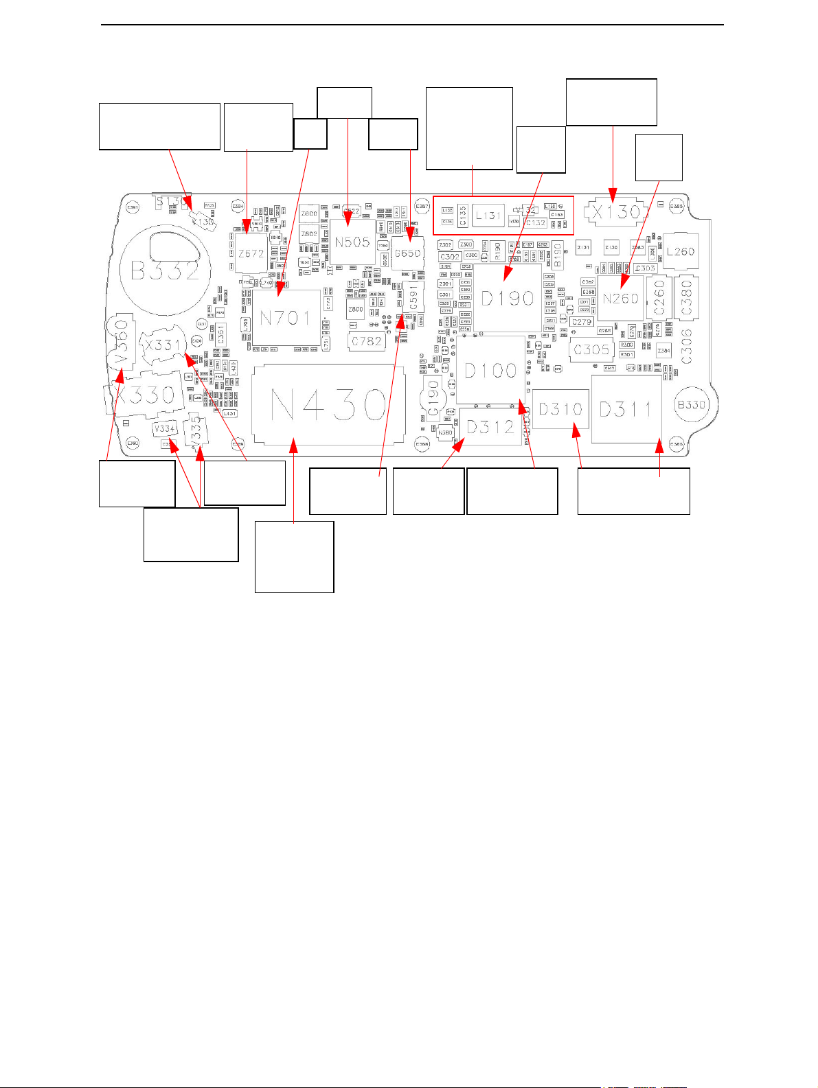
Component placement and PWB outline
Components are placed only on one side of the LG4 module.
Figure 1 shows LG4 module from component side, main components are listed.
Page 8 ¤Nokia Corporation Issue 2 11/02
Page 9
CCS Technical Documentation System Module LG4 and Grip Module LS4
r
r
Figure 1: Main components on LG4
UI module
connecto
AEM
Ambient light
senso
Antenna
switch
PA
Hagar
VCO
UI module
backlight
DC/DC
UEM
IR
Module
Proximity
sensor
Earpiece
Bluetooth
module,
BT102
VCTCXO
64Mbit
SDRA
UPP_WD2
32 + 128
Mbit flashes
Issue 2 11/02 ¤Nokia Corporation Page 9
Page 10
System Module LG4 and Grip Module LS4 CCS Technical Documentation
p
g
p
p
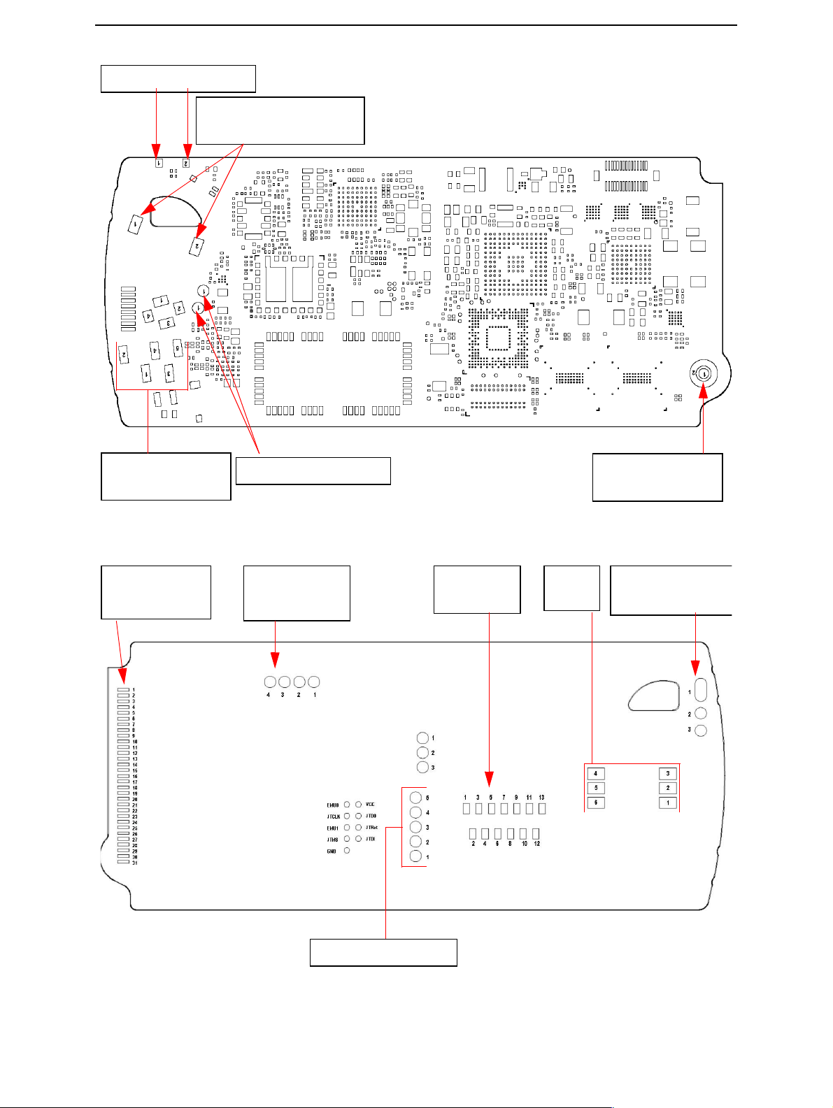
Figure 2: Spring connection pads on top side of LG4
Power switch pads
Integrated handsfree
speaker pads
Headset
connector pads
Flex solder
pads, Grip IF
BT antenna pads
Microphone
ads
Figure 3: Spring connection pads on back side of LG4 and flex cable solder pads
Prod testing:
Powering
Camera
ads
SIM
GSM antenna
ads
Production testin
Page 10 ¤Nokia Corporation Issue 2 11/02
Page 11
CCS Technical Documentation System Module LG4 and Grip Module LS4
Figure 4: Test points in LG4 baseband
Test points of BB
)
J140
(VBAtt)
J262 (UEMRst)
J114 (FLDEX) (mem cntr)
J113 (FLCS0X)
J109 (FLADa0)
J105 (AEMSleepX
J111 (FLCS1x)
J120 (RxQD)
J117 (TxQD)
RF: J118 (AuXDA)
J119 (RxID)
J110 (VcoreA)
J102 (SleepX)
J103 (PURX)
J104 (UEMInt)
J116 (TxID)
J270
(GenV battIO
J138 (Vctrl (camera)
J100 (RFClk)
J101 (Sleepclk)
J106
(SDRDa0)
J115 (FlClk)
J07
(SDR Ad0)
J108
(SDRAMClk)
Issue 2 11/02 ¤Nokia Corporation Page 11
Page 12
System Module LG4 and Grip Module LS4 CCS Technical Documentation
Block diagram
Below is the block diagram of LG4 module. External interfaces are drawn as arrows crossing LG4 border.
Figure 5: Block diagram of LG4
BT
antenna
Flex
to LS4
(Grip)
Flashing & Testing
LG4 module
BB
Sensors
Bluetooth
RF
VGA
camera
UImodule
Audio
SIM card
GSM
antenna
UI Interface
UI module interface pin numbering is presented in figure below. UI interface details are in
UI-module specification.
Figure 6: UI connector pin numbering on LG4 side
Page 12 ¤Nokia Corporation Issue 2 11/02
Page 13

CCS Technical Documentation System Module LG4 and Grip Module LS4
Baseband Technical Summary
The heart of the BB is UPP_WD2, which includes MCU, DSP and Digital Control Logic.
Powering handled by Using AEM ASIC and UEM ASIC. There is Flash Memory 128Mbit +
32Mbit Flashes (20 Mbytes) and 64 Mbit (8 Mbytes) SDRAM. So there is a total of 28
Mbytes of Memory Capacity.
In BB there is an integrated Handsfree Audio Amplifier In AEM. There are two Audio Elements (Earpiece 8 mm and Speaker 16 mm) and External Galvanic Headset (DCT4) interface. IHF Speaker is also used to handle the Ringing tone. For IHF automated off function
there is proximity Sensor. In NHL-2NA there is only one microphone for both modes HS
and IHF.
For Data connectivity there is 1Mbit IR Module (IrDA compatible) and Bluetooth.
Display is MD-TFD type Color Display with 4096 Colors and 176x208 pixels with Backlight. Keyboard is partially in UI-Module and Partially in Grip-Module. Also there is This
Navigation Key Feature in UI-Module.
For imaging purposes BB supports VGA camera via CCP interfaces, which are integrated
in UPP_WD2.
Issue 2 11/02 ¤Nokia Corporation Page 13
Page 14

System Module LG4 and Grip Module LS4 CCS Technical Documentation
Functional Description
BB Description
Core is based on UPP_WD2 CPU, which is a special version of the DCT4 UPP ASIC.
UPP_WD2 takes care of all the signal processing and operation controlling tasks of the
phone as well as all PDA tasks.
For Power management there are two Asics for controlling energy management and supplying current and different voltages; UEM and AEM. UEM and SW have the main control of the system voltages and operating modes and AEM acts as an auxiliary source of
voltages and current. The main reset for the system is generated by the UEM.
The interface from the RF and audio sections is handled also by UEM. This ASIC provides
A/D and D/A conversion of the in-phase and quadrature receive and transmit signal
paths and also A/D and D/A conversions of received and transmitted audio signals. Data
transmission between the UEM, AEM and RF and the UPP_WD2 is implemented using
different serial connections (CBUS, DBUS and RFBUS). Digital speech processing is handled by UPP_WD2 ASIC. Internal HF with proximity sensor functionality is implemented
inside the AEM ASIC.
A real time clock function is integrated into UEM, which utilizes the same 32kHz-clock
source as the sleep clock. A rechargeable battery provides backup power to run the RTC
when the main battery is removed. Backuptime is 20 Hours.
Memory Configuration
NHL-2NA uses two kinds of memories, Flash and SDRAM. These Memories have their
own Dedicated buses in UPP_WD2.
Synchronous DRAM is used as working memory. Interface is 16 bit wide data and 14 bit
Address. Memory clocking speed is 104 MHz. The SDRAM size 64Mbits (4Mx16).
SDRAM I/O is 1.8 V and core 2.78 V supplied by AEM’s regulators VIOA and VMEMA. All
memory contents are lost if the supply voltage is switched off.
Multiplexed Flash Memory Interface is used to store the MCU program code and User
Data. The memory interface is a burst type FLASH with multiplexed address/data bus.
Both I/O and core voltage are 1.8 V supplied by AEM’s VMEMB.
Energy Management
The master of EM control is UEM and with SW they have the main control of the system
voltages and operating modes. AEM (Auxiliary Energy Management) acts as an auxiliary
source of voltages and current.
Page 14 ¤Nokia Corporation Issue 2 11/02
Page 15
CCS Technical Documentation System Module LG4 and Grip Module LS4
Modes of Operation
NHL-2NA employs several hardware & SW controlled operation modes. Main Modes are
described below.
• NO_SUPPLY mode means that the main battery is not present or its
voltage is too low (below UEM master reset threshold) and back-up battery voltage is too low.
• In BACK_UP mode the main battery is not present or its voltage is too
low but back-up battery has sufficient charge in it.
• In PWR_OFF mode the main battery is present and its voltage is over
UEM master reset threshold. All regulators are disabled.
• RESET mode is a synonym for start-up sequence and contains in fact
several modes. In this mode regulators and oscillators are enabled and
after they have stabilized system reset is released and PWR_ON mode
entered.
• In PWR_ON mode SW is running and controlling the system.
• SLEEP mode is entered from PWR_ON mode when the system’s activity is low (SLEEPX and AEMSLEEPX controlled by SW).
• FLASHING mode is for production SW download.
Voltage limits
In the following the voltage limits of the system are listed. These are also controlling system states.:
Parameter Description Value
V
MSTR+
V
MSTR-
V
COFF+
V
COFF-
V_BU
COFF+
Master reset threshold (rising) 2.1 V (typ.)
Master reset threshold (falling) 1.9 V (typ.)
Hardware cutoff (rising) 3.1 V (typ.)
Hardware cutoff (falling) 2.8 V (typ.)
Back-up battery cutoff (rising) 2.1 V (typ.)
V_BU
SW
COFF
COFF-
Back-up battery cutoff (falling) 2.0 V (typ.)
SW cutoff limit (> regulator drop-out limit) MIN! 3.15 V SW changeable
The master reset threshold controls the internal reset of UEM. If battery voltage is above
, UEM’s charging control logic is alive. Also, RTC is active and supplied from the
V
MSTR
main battery. Above V
UEM allows the system to be powered on although this may
MSTR
not succeed due to voltage drops during start-up. SW can also consider battery voltage
Issue 2 11/02 ¤Nokia Corporation Page 15
Page 16
System Module LG4 and Grip Module LS4 CCS Technical Documentation
too low for operation and power down the system.
Clocking Scheme
A 26 MHz VCTCXO is used as system clock generator in GSM. During the system start-up,
UEM and AEM use their own RC-oscillators to generate timing for state machines. All
clock signals of the engine are illustrated in following figure.
In PWR_ON mode, SW must configure CBUS clock (1MHz) to be active all the time, as
this clock is used in AEM as digital clock and for the SMPS. Bluetooth uses 26 MHz analog clock.
Figure 7: NHL-2NA Clocking.
RF
26 MHz
VCXO
RF-ASIC
(Hagar)
RFClk
13 MHz
RFBusCl
UPP_WD2 UEM
SleepClk
CBusCl
DBusCl
SIMCl
SIM
Flash
Clk
LPRF
FLASHes
CAMERA
In SLEEP mode the VCTCXO is off. UEM generates low frequency clock signal (32.768
kHz) that is fed to UPP_WD2, Bluetooth and AEM.
UPP_WD2 voltage/clock frequency adjusting
The systems of the BB make it possible to adjust both clock frequency and the core voltage of the main ASIC. Here is a rough description of the Clocking Scheme.
No external clock is available for UPP_WD2 before VCTCXO starts. As reset is released,
the VCTCXO is running and MCU uses the 13 MHz clock while DSP is in reset. There are
three identical DPLL's, for MCU, for DSP and for accessory interfaces, which can be controlled independently. The clock for MCU can be up to 104 MHz and 117 MHz is maximum clock Frequency for the DSP. These clock signals are used either directly (SDRAM IF)
or divided down for the interfaces (e.g. flash IF).
SDRAM
Clk
SDRAM
AEM
Page 16 ¤Nokia Corporation Issue 2 11/02
Page 17
CCS Technical Documentation System Module LG4 and Grip Module LS4
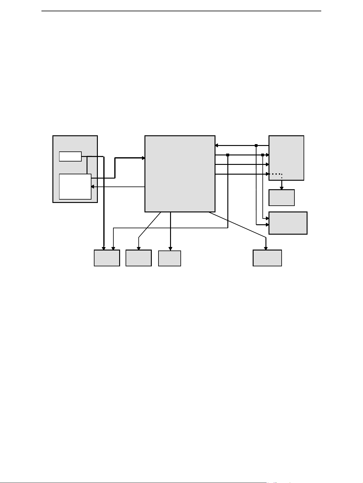
Power Distribution, Control and Reset
All power (except backup battery power) is drawn from BLB-2 Li-Ion battery located in
the Grip part of the phone. Power goes through LM3822 current gauge which is used for
current measurement and thus for remaining operating time estimation.
LG4 board contains two power ASIC’s UEM and AEM which contain the regulators
needed for generating the different operating voltages. In addition there is a SMPS in
LG4 generating the operating voltage for display module backlighting. In LS4 keyboard
the backlight is powered with a current pump.
Figure 8: Power distribution diagram
Issue 2 11/02 ¤Nokia Corporation Page 17
Page 18

System Module LG4 and Grip Module LS4 CCS Technical Documentation
Power-up sequence (Reset mode)
RESET mode can be entered in four ways: by inserting the battery or charger, by RTC
alarm or by pressing the power key. After voltage appearing at UEM’s pin UEMRSTX (connected to AEM’s pin REFENA) is used as indication for AEM to start up HW regulators.
Also VCTXO is Powered up by using VR3 (UEM). After the 220 ms delays regulator are
configured and UEM enters PWR_ON mode and system reset PURX is released.
During system start-up, in RESET state, the regulators are enabled, and each regulator
charges the capacitor(s) at the output with the maximum current (short circuit current)
it can deliver. This results in battery voltage dropping during the start-up. When a battery with voltage level just above the hardware cutoff limit is inserted, the system may
not start due to excessive voltage dipping. Dropping below 2.8 V for longer than 5 us
forces the system to PWR_OFF state.
Powering off
Controlled powering off is done when the user requests it by pressing power-key or when
the battery voltage is falling too low. Uncontrolled powering off happens when battery is
suddenly removed or if over-temperature condition is detected in regulator block while
in RESET mode. Then all UEM’s regulators are disabled immediately and AEM’s regulators
are disabled as VDD supply disappears.
Controlled powering off
For NHL-2NA powering off is initiated by pressing the power key and Power off sequence
is activated in UEM and SW. Basically Power key cause UEM Interrupt to UPP_WD2 and
SW sets Watchdog time value to zero and as this happens, PURX is forced low and all
regulators are disabled.
If the battery voltage falls below the very last SW-cutoff level, SW will power off the
system by letting the UEM’s watchdog elapse.
If thermal shutdown limit in UEM regulator block is exceeded, the system is powered off.
System reset PURX is forced low. AEM has its own thermal limit for regulators. Whenever
the limit is exceeded, an interrupt is given to UPP_WD2 and SW should immediately
power off the whole system. AEM will disable its regulators in any case by itself after 10
ms delay (uncontrolled powering off).
Uncontrolled powering off
This happens when the battery is suddenly removed and is problematic as data may corrupt in memories. UEM’s state machine notices battery removal after battery voltage has
been below V
COFF-
regulators are disabled. AEM’s regulators except for VCOREA, VIOA, VMEMA and VMEMB
are disabled as PURX goes low. These regulators stay enabled as long as there is voltage
present at pin VDD (from UEM’s VIO).
for 5 us and enters PWR_OFF mode. PURX is set low and all UEM’s
Watchdogs
There are three watchdogs in UEM. First one is for controlling system power-on and
power-down sequences. The initial time for this watchdog after reset is 32 s and the
Page 18 ¤Nokia Corporation Issue 2 11/02
Page 19

CCS Technical Documentation System Module LG4 and Grip Module LS4
watchdog can not be disabled. The time can be set using a register. This watchdog is used
for powering the system off in a controlled manner. The other one is for security block
and is used during IMEI code setting. The third one is a power key watchdog. It is used to
power off the system in case SW is stuck and the user presses the power key. This WD is
SW configurable.
There is also a ”soft watchdog” in UPP_WD2. It is used to reset the chip in case software
gets stuck for any reason. The Bluetooth module also contains a watchdog.
Charging
Charging controls and charge switch is in UEM. There are three different charging
modes; charging empty battery (start-up charge mode), PWM charging mode (without
SW control) and SW controlled charging.
UEM digital part takes care of charger detection (generates interrupt to UPP_WD2),
pulse width modulated charging control (for internal charge switch and external performance charger) and over voltage and current detection. SW using registers controls all
these.
Chargers
Battery
NHL-2NA BB is supporting a standard charger (two wires) or fast (performance) charger
(three wires), Chargers ACP-7, ACP-8 and ACP-9 and ACP-12, Cigarette Charger LCH-8
are supported.
With the standard version the PWM signal is set to 1 Hz, while with fast charger it is set
to 32 Hz. Also PWM signal is connected from UEM pin to the charger’s control input.
Due to high current consumption of the NHL-2NA BB, a performance charger ACP-8 is
needed.
NHL-2NA Battery is a detachable, semi-fixed Lithium-Ion BLB-2 battery. Other batteries
are allowed to use but NOT charged. Nominal voltage is thus 3.6-3.7 V (max charging
voltage 4.1-4.2 V).
The interface consists of four pins: VBAT, GND, BSI and BTEMP. Pull-down resistor inside
of the batteries (BSI signal) recognizes the battery types. Voltage level at BSI line is measured with using Em's AD-converter.
Issue 2 11/02 ¤Nokia Corporation Page 19
Page 20

System Module LG4 and Grip Module LS4 CCS Technical Documentation
Back-up battery and real time clock
Real time clock (RTC), crystal oscillator and back-up battery circuitry reside in UEM. A
register in UEM controls back-up battery charging and charging is possible only in
POWER_ON State.
Baseband Measurement A/D Converter
The UEM contains 11 channels A/D converter, which is used for different Baseband measurement purposes. The resolution of A/D converter is 10 bits. Converter uses the CBUS
interface clock signal for the conversion. An interrupt will be given to the MCU at the
end of the all measurement. Converter is used for following purposes.
• Battery Voltage Measurement A/D Channel (Internal)
• Charger Voltage Measurement A/D Channel (Internal)
• Charger Current Measurement A/D Channel (Internal)
• Battery Temperature Measurement A/D Channel (External)
• Battery Size Measurement A/D Channel (External)
• Light Sensor Measurement A/D Channel (External)
• PA Temperature measurement A/D Channel (External)
• VCTCXO Temperature measurement A/D Channel (External)
There is also auxiliary AD converter in UEM, which is used to monitor RF functions. Converter is controlled directly by UPP DSP. Converter can be used for following purposes:
VCXO Temperature measurement A/D Channel (if not used in normal AD)
PA Temperature measurement A/D Channel (if not used in normal AD)
Page 20 ¤Nokia Corporation Issue 2 11/02
Page 21

CCS Technical Documentation System Module LG4 and Grip Module LS4
NHL-2NA BB Features & HW interfaces
NHL-2NA BB User interface
UI-Module Interface
Interface is for Color Display 176 x 208 (X3) resolution and backlight is white LED with
lightguide. Also Part of Keyboard is locating in module with Navigation Key. Display is
connected to LG4 by 30-pin Board-to-Board connector. Interface includes also power
rails for UI and Backlight. Interface uses GPIO pins of UPP_WD2.
Power Key
PWROnx of UEM is pulled up to battery voltage by a current source inside UEM. Pressing
PWR-Key connects UEM PWRONX-pin to ground via resistor. The power key has also a
reset function: while removing battery is difficult, a reset can be accomplished by pressing this key for longer time. Power key is connected to main PWB via spring contacts.
Grip Interface
Grip Interface includes Matrix Keyboard & Backlight, Battery interface, Vibra Interface,
Charger interface, Current Gauge interface.
Hall Sensor and Magnet
NHL-2NA is using Hall sensor TLE 4917 (NMP code 4341087) and magnet to find out the
open/close position of the grip. The hall sensor component is in the LG4 BB area and the
magnet is in the grip module. See locations of the sensor and magnet below, figure 9.
As the grip is closed, the hall sensor and magnet are against each other. At this position
the output of the hall sensor is high. As the grip is open and sensor and magnet are separated, the output is low. This low level gives the information to processor that grip is
open.
Figure 9: Locations of the sensor and magnet
Transceiver
LG4
Hall sensor
Grip
LS4
Magnet
Sensor needs 2.7V for operation and that's why Vflash1 voltage is needed to be connected to Vs pin. PRG pin is needed to be connected GND that output is zero as magnet
and sensor are separated. See Principle of the connection of the hall sensor below.
Issue 2 11/02 ¤Nokia Corporation Page 21
Page 22

System Module LG4 and Grip Module LS4 CCS Technical Documentation
Figure 10: Principle of the connection of the hall sensor
Vflash1
100nF
PRG GND GND
Vs GND Q
GenIO25
10pF
UPP_WD2
Pins list of Hall sensors:
Pin Min Nom Max Pin number
Vs 2.4 V 2.7 V 3.5 V 1
GND 0 V 2, 4, 5
Q 0 V 1.8 V 3
PRG 0 V 3.7 V 6
Page 22 ¤Nokia Corporation Issue 2 11/02
Page 23

CCS Technical Documentation System Module LG4 and Grip Module LS4
A
Bluetooth
Bluetooth provides a fully digital link for communication between a master unit and one
or more slave units. The system provides a radio link that offers a high degree of flexibility to support various applications and product scenarios. Data and control interface for
a low power RF module is provided. The transmission is half-duplex. Air bit rate is 812.5
kbit/s.
IR
NHL-2NA BB uses TDFU5102 1Mbit IrDA 1.1 compatible module. Module interface signals are Tx (Transmitted Data), Rx (Received Data) and SD (ShutDown). IR transmission data speed can be from 9.6 kbit/s to 1.15 Mbit/s. The communication over the
IR is always started using bit rate 9.6 kbit/s. and the maximum we use is 115kbit/s.
Digital part is powered with 2.78 V by VMEMA and the LED by VBAT (nom. 4.2 V).
VMEMA is fully SW-controlled regulator. More details of the module can be found out
from IR specification under EDMS. See figure 11 for
Figure 11: IR connected to UPP_WD2
SIM Interface
The SIM interface is located in two chips (UPP_WD2 and UEM). In UEM there is only
support for one SIM card. The interfaces support both 1.8 V and 3 V SIM cards. Adjustable SIM regulator (1.8V/3.0V) is located in UEM and can be controlled by SW.
UPP_WD2
I IR
Block
1.8V
EM
2.7V
Module
TDFU5102
VCC
IREDA
RXD
TXD
SD
GND
IREDC
The data communication between the card and the phone is asynchronous half duplex.
The clock supplied to the card is in GSM system 1.083 MHz or 3.25 MHz. The data
baudrate is SIM card clock frequency divided by 372 (by default), 64, 32 or 16.
Issue 2 11/02 ¤Nokia Corporation Page 23
Page 24

System Module LG4 and Grip Module LS4 CCS Technical Documentation
NHL-2NA Audio Concept
NHL-2NA Audio's includes Earpiece, microphone, and headset connector, Integrated
Handsfree (IHF) with proximity sensing. IHF have high quality Audio with DCT4 Enchantments. Headset is DCT4 monoheadset with/-out button. For IHF versus Earpiece function
there is proximity sensor option, which detects if close to head, it switches IHF off. It can
be turned ON Manually by pressing the voice key. In NHL-2NA Audio Blocks there is
NHL-2NA BB Audio block diagram. Audio's are based on ASIC's UPP_WD2 and UEM.
Figure 12: NHL-2NA Audio Blocks
Earpiece
This Asic's readily support normal audio functionality. Between UPP_WD2 and UEM the
audio signals are transferred in digital format using signals MICDATA and EARDATA. The
microphone is connected to UEM and the headset output of UEM is fed also to AEM
audio amplifier. So actual IHF situation the signal is also existing in Headset signals.
NHL-2NA audio SW controls IHF amplifier power off when uses headset because both
use same audio lines (HF and HFCM). Ringing tones and warning/info tones are to be
produced with the IHF speaker also.
The earpiece to be used in NHL-2NA is an 8-mm Pico earpiece. It has 32: continuous
impedance and continuos power 8 mWatts. It Contacts to PWB Special adapter via
springs. It's driven by differential signals from UEM (EARP & EARN)
Page 24 ¤Nokia Corporation Issue 2 11/02
Page 25

CCS Technical Documentation System Module LG4 and Grip Module LS4
Microphone
The microphone capsule for NHL-2NA is a WM64MN capsule. Its sensitivity is -41db
Nominal and it's provided encapsulated in housing of neoprene. Contacts are done by
springs.
Two inputs are used from UEM, one for normal internal microphone and a second for
headset. The third microphone input is not used, so it must connected to ground. Microphone bias block in UEM generates bias voltages for handportable and HandsFree/headset microphones. For both microphone bias outputs (MICB1 & MICB2) the minimum
output voltage is 2.0 Volts and maximum output current is 600 PA. Microphone bias
block also includes a low pass filter for the reference voltage used as an input for the
MICB1&2 amplifiers.
IHF Amplifier and Speaker
The speaker to be used in NHL-2NA is a 16mm 8: speaker. It can handle 0.2 Watts nominal Power and Peak power 0.4 Watts. Component has molded neoprene gasket and its
contact to PWB via springs.
HF and HFCM lines of UEM are use to drive AEM IHF amplifier. IHF amplifier consists of
four blocks: gain setting stage, power amplifier, and comparator and Bias VCM generation. There is also some digital logic, which is integrated to other digital parts of AEM.
Power amplifier is a differential opamp. The differential output is intended to HandsFree
speaker. HandsFree amplifier load impedance is 8 ohm.
The outputs go into a high impedance state when powered down. The amplifier can be
enabled and shut down by control register.
SW realizes IHF and earpiece volume control mainly in AEM. For maximum signal–to–
noise performance it is preferable to set the gain of UEM’s earpiece driver to some fixed,
close–to–maximum value and use lower gain setting for AEM audio amplifier. Gain setting can be done in 2 dB steps, from –40 to +6 dB. Output sound pressure level of the
internal HandsFree speaker is controlled by the proximity sensor and SW (CBus is used
for controlling). Proximity sensor activity changes the gain automatically.
The schematic around the AEM IHF amplifier is presented in NHL-2NA schematics. The
schematic shows all the filtering needed and also protection components against ESD
and EMC.EMC and ESD Filtering component must be as near as possible to earphone
pads of the phone. Audio input lines components DC decoupling capacitors and EMC
capacitor must be located near to AEM.
The supply voltage for the IHF amplifier is filtered directly from the battery voltage. The
size of the capacitance needed for smoothing the voltage is High-Pass filter consist of
two parallel 220uF capacitors to ground with 2x2.2Ohm parallel in Series in VBAT line.
Issue 2 11/02 ¤Nokia Corporation Page 25
Page 26

System Module LG4 and Grip Module LS4 CCS Technical Documentation
External Audio interface
In NHL-2NA there is Headset Connector which is fully differential 4–wire connection.
Figure 13: External Audio Connector
2. XEARN
4. XEARP
5. HEADINT
3. XM ICP
1. XM ICN
The Handsfree (HF) driver in UEM is meant for headset. In NHL-2NA case the output is
driven in fully differential mode. In the fully differential mode HF pin is the negative output and HFCM pin is the positive output. The gain of the Handsfree driver in the differential mode is 6 dB. The earpiece (EARP, EARN) and headset (HF, HFCM) signals are
multiplexed so that the outputs can not be used simultaneously. Minimum resistive and
maximum capacitive loading between HF and HFCM outputs are 30ohm
and 10nF. The
HF and HFCM amplifiers include a transient suppression circuitry, which prevents
unwanted spikes in HF and HFCM outputs when switching on and off the amplifiers.
The plug opens a mechanical switch inside the connector between HF and HeadInt lines.
The HeadInt line will be pulled up to 2.7V by internal resistor when the switch is open.
When not having the plug inserted the voltage in the HeadInt line will be <0.8 V caused
by internal pull down resistor in the HF line.
Camera Interface
NHL-2NA camera type is a Still camera with viewer option. Camera resolution is VGA.
The Camera module is connected by springs to PWB.
Camera interface is serial CCP, which is unidirectional interface; the control information
to camera is transmitted through I2C bus. The I2C is implemented purely by SW using
general purpose I/Os.
CCP interface consists of differential type of clock signal and one data signal. CCP
enables the use of high data rates with low EMI; maximum transfer capacity is 104 Mbit/
s, which means that transferring VGA (640x480) images at 15 fps is possible. CCP has
three image data operating modes: 8-bit, 10-bit and 12-bit ones.
AEM includes two dedicated regulators for powering internal camera, 2.78V for logic and
sensor and 1.8V for I/O.
More about camera module later in this section.
Page 26 ¤Nokia Corporation Issue 2 11/02
Page 27

CCS Technical Documentation System Module LG4 and Grip Module LS4
Proximity Sensor
Proximity Detector is used to deactivate IHF when something is close to the phone. Proximity detection is based on detecting level of reflected IR radiation. Detection distance
varies depending on the reflecting surface. System is calibrated to detect 20% diffuse
reflectance targets, parallel to the phone, at 50mm distance. Detection distance may
change due to wearing; minimum detection distance allowed is 30mm.
Figure 14: Proximity Detector Principle
Reflective Su rface
Li
gh
tg
ui
IR-LE D IR-Detector
Li
gh
tg
ui
Cover
PWB
Proximity Detector has also a self-monitoring feature, which is used to detect possible
failures in the Proximity Detector. Proximity Detector Principle figure describes the
mechanical concept of the Proximity Detector, Pulse levels shows signal levels.
Figure 15: Pulse levels
Proxi mity det ect
pulse
Self-test
puls e
Detecti on Treshold
Fault Treshol d
Faul t detect
puls e
Proximity detector interface is in AEM (Auxiliary Energy Management ASIC), other components of the proximity detector are optoelectrical components and optics.
The proximity detector block on AEM consists of digital and analog part. Digital logic is
included in digital part of AEM, and it is controlled through proximity detector control
register.
Analog part includes a current source for the emitter and a transinpedance amplifier,
high pass filter to filter off up to 2mA DC-current, gain-controllable amplifier and two
Issue 2 11/02 ¤Nokia Corporation Page 27
Page 28

System Module LG4 and Grip Module LS4 CCS Technical Documentation
comparators with adjustable thresholds in the receiver.
Proximity detector block enables several pulse width and pulse frequency selections and
emitter current can be controlled with a current sensing resistor. In NHL-2NA emitter
current is 100mA, pulse width 8Ps and pulse frequency 500/2000Hz.
Proximity Detector components
Lightguides
Lightguides are needed to guide emitted IR radiation outside the phone as well as to
guide the reflected pulses into the phone to the photodiode. Half angle of the emitted
radiation is 10q. This means, that most of the emitted radiation is reflected from a circle
that has diameter 20mm, when the target is at 50mm distance. Receiver lightguide collects radiation and guides it to the photodiode. Optical insulator, made of black rubber,
surrounds the photodiode so that it cannot receive any radiation that is reflected inside
the phone.
Self-monitoring signal is created with small reflector areas and curved top surfaces in
the lightguides. Reflectors are placed inside the phone, so that they are subject to as little wearing as possible.
IRED
The IRED type is CL-200-IR-X-TU (NMP CODE 4860009), which has high radiant intensity
and relatively small half angle (28°). Maximum forward current is 100mA (pulsed 1A) and
V
=1.3V. Rise Time is 2Ps, total radiant intensity 12mW (at 50mA current) and peak
f
radiant intensity at 950nm.
Photodiode
The photodiode is BPW34FS (NMP CODE 486J830). It has peak sensitivity at 950nm and
filtering for visible light. Photodiode receives radiation from 60° half angle and its rise
time is 20ns.
HW Implementation
The implementation of the proximity sensor is described in figure 16. Note that VTOUCH
is connected externally to VANA.
Page 28 ¤Nokia Corporation Issue 2 11/02
Page 29

CCS Technical Documentation System Module LG4 and Grip Module LS4
Figure 16: Proximity sensor implementation
VTOUCH
(2.78V)
VBAT
VANA
(2.78V)
AEM
IRED
4.7 Ohm
PRXdrv
PRXin
IR Detector
GNDANA
PRXrec
COFF CF1 CF2
100nF 220pF 220pF
Issue 2 11/02 ¤Nokia Corporation Page 29
Page 30

System Module LG4 and Grip Module LS4 CCS Technical Documentation
Ambient Light Sensor
Ambient Light Detector (ALD) is used as a power saving feature.
Ambient Light Detector (ALD) measures illuminance on the display (ambient light). User
can select the limit, above which display backlight is not needed. In practice, two limits
are used in software to produce hysteresis. Hysteresis is needed to prevent backlight
from blinking. Backlight can be switched ON only when ambient light level is below
lower limit. Backlight is switched OFF, when ambient light level exceeds higher limit.
Figure 17: Ambient light sensor implementation
Ambient
Light
Optical
Lense
VFlash1
2.78 V
Pull-up
resistor
100 kOhm
Phototransistor
Siemens
LS
UEM
VCXOTEMP
VANA
2.78 V
Pull-up
resistor
100 kOhm
NTCResistor
Page 30 ¤Nokia Corporation Issue 2 11/02
Page 31

CCS Technical Documentation System Module LG4 and Grip Module LS4
V
Flashing
SW download in service is impelemented by custom tools and SW, kindly refer to Service
Software Instructions and Service Tool section of the manual.
Connections to Baseband
NHL-2NA type flash programmer FPS-8 is connected to the baseband directly in Production Tester, by using service cable and FLA-21 or Module jig to connect to test pads. With
assembled devices the testpads can be accessed by opening the grip with a special tool.
Figure 18: Flash programming connections
PurX
PC
LPT1
Serial2(AXS-4)
FPS 8 ONLY)
Centronics
FPS-8 /FLS-4S
(
ACF-8
COM2
COM1
Phone
service cable
2.78V
Vpp
Gnd
BSI
MBUS
FBUS_RX
FBUS_TX
cc
UEM
MBUS
FBUS
BSI
GND
TXRX
Flashing interface
FBUS_TX MBUS
FBUS_RX
2.78V
VPP
MBUS_RX
MBUS_TX
FBUS_RX
FBUS_TX
1.8V
UPP_WD2
4k7
Vpp
Flash
= DCT4 Accessories
= Phone
FPS-8 can also supply Vcc during flash programming i.e. service box’s or service battery’s
Vcc can be connected to FPS-8 by banana plugs but external power supply can be also
used during flash programming. shows how flash programming equipment is connected.
Note that Vcc connected to FPS-8/FLS-4S is preferred.
The flash programming interface uses following external signals:
1 FBUS RX (accessed from test pad pattern)
2 FBUS TX (accessed from test pad pattern)
3 MBUS (accessed from test pad pattern)
Issue 2 11/02 ¤Nokia Corporation Page 31
Page 32

System Module LG4 and Grip Module LS4 CCS Technical Documentation
4 BSI (accessed from battery connector)
5 Vcc (accessed from battery connector)
6 Ground (accessed from test pad pattern and battery connector)
7 Vpp (accessed from test pad pattern)
In HDB15 BB Vpp routing is based on common DCT4 solution. In this solution the use of
higher Vpp voltage is enabled at FLALI phase in production and in after sales if so
wanted.
External voltage (Vpp) is used during flash programming in production and possibly in
aftersales to speed up the process. In production, the usage of external programming
voltage is a necessity but in after sales the usage of external programming voltage does
not necessarily bring any noticeable improvement to flash programming time.
Testing interfaces
In NHL-2NA BB Interfaces Because of Camera, larger memory, sensors there are some
specific testing done and also because of flagship concept there is difference of physical
Interfaces
Table 1: Testing interface Electrical Specifications
Pin Name Dir Parameter Min Typ Max Unit Notes
1 MBUS <-> Vol 0 0.2 0.3*VFlash1 V
Vil (From Prommer) 0 0.2 0.3*VFlash1 V
Voh 0.7*VFlash1 2.7 0.7*VFlash1 V
Vih(From Prommer) 0.7*VFlash1 2.7 VFlash1 V
2 FBusTx -> Vol 0 2.7 0.3*VFlash1 V
Voh 0.7*VFlash1 2.7 VFlash1 V
3 FBusRx <- Vil (From Prommer) 0 2.7 0.3*VFlash1 V
Vih(FromPrommer) 1.89 2.7 VFlash1 V
Abs. Max. Voltage to
Test Pad Referenced
to GND
4 VPP To Phone 0 / 2.8 / 12
-0.3V 3.0 V Absolute
Max Voltage
limits to
MBUS/FBUS
+/-3%
V Prommer
Select
4 VPP
4 VPP To Phone 0 / 2.8 / 12
+/-3%
5 GND 0 V VBAT
V Prommer
Select
4 VPP
GROUND
Note1: VFlash1 is 2.78 +/- 3%
Page 32 ¤Nokia Corporation Issue 2 11/02
Page 33

CCS Technical Documentation System Module LG4 and Grip Module LS4
Table 2: Electrical Specifications for Power Supply Interface in Prod Testing
Pin Name Min Typ Max Unit Notes
1 VBAT 0 3.6 5.1 V
2 BSI 0 2.78 VFlash1 V Internal pullup
3 BTEMP 0 3.0 VAna V Internal pullup
4 GND 0 V
Note 1: VAna & VFlash1 = 2.78 +/-3%
Extreme Voltages
Lithium-Ion battery BLB-2 (1 cell):
• Nominal voltage is 3.6V
• Lower extreme voltage is 2.8V (cut off voltage)
• Higher extreme voltage is 4.2V (charging high limit voltage)
Temperature Conditions
Specifications are met within range of –10C to +55C ambient temperature. Reduced
operation between [-25] and [+60]. Storage temperature range is of –40C to +85C
according to Nokia specifications.
Humidity and Water Resistance
Relative humidity range is 5 … 95%. Condensed or dripping water may cause intermittent malfunctions. Protection against dripping water have to be implemented in (enclosure) mechanics. Continuous dampness will cause permanent damage to the module.
Issue 2 11/02 ¤Nokia Corporation Page 33
Page 34

System Module LG4 and Grip Module LS4 CCS Technical Documentation
RF Module
Functional block descriptions
The block diagrams of direct-conversion receiver and transmitter RF section are
described in the following figure. The illustration shows the RF-IC ( both RX and TX
functions ), power amplifier ( PA ), TX-SAW filter, VCO, VCTCXO module, discrete LNA
stages and SAW-filters for receive bands.
Figure 19: RF block description
VR4
Antenna switch
Dir. Coupler
GSM
1800
E-GSM
900
DET
RX
SAW
TX
RX
SAW
TX
VtxLO_GS M
PA
VBATTRF
LNA
LNA
VtxB_DCS
VtxB_GSM
dB
-2
dB
-2
Last edit 12:39 1 3.12.00
Drawing85
VRF_RX
SAW
INP_P_RX
INM_P_RX
SAW
INP_G_RX
INM_G_RX
LNA_P
LNAB_P
LNA_G
LNAB_G
V_ANT_1/
V_ANT_2
2
VB_DET
VTXLO_G
VTX_B_P
VTX_B_G
OUTP_P_TX
OUTM_P_TX
OUTP_G_TX
OUTM_G_TX
Vpctrl_ fb
RF
Controls
Open collecto r
Open collecto r
DET
Vpctrl_g
Vpctrl_p
2
1/4
PWC
TXP
TXC
222
1/2
2
2
2
44
0dB
Cm_dtos_I
1/2
1/4
44
2
2 2
RX Filter
Calibration
8 / 18 dB
8 / 18 dB
Reset
Cp_dtos_I
DtoS
DtoS
64/65
CTRL
SDATA
Cp_f_I
Cm_f_I
Cp_f_Q
Cm_f_Q
Cp_dtos_Q
Cm_dtos_Q
BIQUAD
BIQUAD
NDIV
ADIV
HAGAR
SLE
SCLK
OUT_BB1_I
OUT_BB1_Q
I_DCN2_I
charge
pump
RDIV
I_DCN2_Q
C2_BB1_Q
C1_BB1_Q
VB_EXT
DCN2
DCN2
1/2
RF TEMP
SENSOR
RB_EXT
VF_RX
RXI
VREF_RX
RXQ
INP_LO/INM_LO
2
OUT_CP
loop
filter
VCP/GND_CP
2
VDIG
OSC_IN
26MHz
TOUT
VBB
VPRE
VLO
TXI_0/TXI_180
2
TXQ_0/TXQ_180
GNDRF_TX
GND_BB / GNDRF_RX / GND_L O / GND_PRE /
GND_CP / GND_ DIG / GND_ RX
RFTEMP
C1_BB1_I
C2_BB1_I
BB_Gain
0-40dB
BB_Gain
0-40dB
M
VREFRF01
RXI_P
RXI_N
VREFRF02
RXQ_P
RXQ_N
VR1
VCO
3dB
VR7
2
2
LPRFCLK
RFCLK
TXI_0/TXI_180
TXQ_0/TXQ_180
HGR_TEMP
RFBUSEN1
RFBUSCLK
RFBUSDA
RESET
VBATTRF
VR3
AFC
VR6
VR5
TXC
TXP
VR2
AFC
The Frequency synthesizer
The VCO frequency is locked using a PLL to a stable frequency source, which is a VCTCXO.
The VCTCXO is running at 26 MHz. The Temperature effect is controlled with AFC. The
AFC is generated with a 11 bit conventional DAC in UEM.
The physical PLL is located inside the HAGAR RF-IC and is controlled via serial bus. The
PLL synthesizer consists of the following blocks :
• 64/65 CML prescaler
• Programable R-, N- and A-dividers,
• Phase detector and charge pump
Page 34 ¤Nokia Corporation Issue 2 11/02
Page 35

CCS Technical Documentation System Module LG4 and Grip Module LS4
Figure 20: Phase locked loop
HAGAR
GSM1800
O2
3420 - 3840 MHz
E-GSM900
AFC
26 MHz
O4
SDATA
CTRL
SCLK
O64/65
SLE
NDIV
ADIV
RDIV
( O65 )
Reset
M
Charge
Pump
Loop
Filter
VCO
The SHF local signal generated by a VCO module is fed into prescaler. The prescaler is a
dual-modulus divider. The output of the prescaler is fed to N- and A- divider which produce the input to phase detector. The phase detector compares this signal to the reference signal (400 kHz) which is obtained by dividing the VCTCXO output by reference Rdivider. The output of the phase detector is connected to the charge pump which charges
or discharges integrator capacitor in the loop filter, depending on the phase of the measured frequency compared to the reference frequency.
The loop filter, VCO and VCTCXO are all external synthesizer building blocks.
The loop filter performs filtering of the pulses and generates DC control voltage to the
VCO. The loop filter also defines the step response of the PLL ( settling time ) and effects
the stability of the loop. That’s why integrator capacitor has got a resistor for phase
compensation. The other filter components are for sideband rejection.
The dividers are controlled via serial bus: SDATA is for data, SCLK is serial clock for the
bus and SLE is latch enable, which enables new data storage into dividers.
The transceiver LO signal is generated by VCO module. The VCO generates double frequency in GSM1800 and times four frequency in E-GSM900 compared to the actual RF
channel frequency. LO signal is divided by two or four in HAGAR ( depending on system
mode ).
This RF module comprises all RF functions of the engine. RF circuitry is located on one
side (B-side) of the PCB.
EMC leakage is prevented by using a metal B-shield, which screens the whole RF side
(included FM radio) of the engine. The conductive (silicon or metal) gasket is used
between the PCB and the shield. The metal B-shield is separated to three blocks. The first
one include the FM radio. The second block include the PA, antenna switch, LNAs and
dual RX SAW. The last block include the Hagar RF IC, VCO, VCTCXO, baluns and balanced
filters.
Issue 2 11/02 ¤Nokia Corporation Page 35
Page 36

System Module LG4 and Grip Module LS4 CCS Technical Documentation
The baseband circuitry is located on the A-side of the board, which is shielded with a
metallized frame and ground plane of the UI-board.
Maximum height inside on B-side is 1.8 mm. Heat generated by the circuitry is conducted out via the PCB ground planes and metallic B-shield
RF Frequency Plan
Figure 21: RF Frequency plan
925–960
MHz
1805–1880
MHz
1710–1785
MHz
880–915
MHz
f/4
f
f
HAGAR
f
f/2f/4
f
f/2
PLL
3420–
3840
MHz
26 MHz
VCTCXO
I–signal
I–signalI–signalI–signal
Q–signal
I–signal
Q–signal
RX
TX
Page 36 ¤Nokia Corporation Issue 2 11/02
Page 37

CCS Technical Documentation System Module LG4 and Grip Module LS4
DC characteristics
Regulators
List of the needed supply voltages :
Volt. source Load
VR1a PLL charge pump (4,8 V)
VR2 TX modulator
VR3 VCTCXO + buffer
VR4 HAGAR IC (LNAs+mixer+DTOS)
VR5 HAGAR IC (div+LO-buff+prescaler),
VR6 HAGAR (Vdd_bb)
VR7 VCO
VrefRF01 ref. voltage for HAGAR
VrefRF02 ref. voltage for HAGAR
Vbatt PA
Issue 2 11/02 ¤Nokia Corporation Page 37
Page 38

System Module LG4 and Grip Module LS4 CCS Technical Documentation
Power Distribution Diagram
Figure 22: Power Distribution Diagram
UEM
VR
1
VR
2
VR
3
VR
4
VR
5
E-GSM900/GSM1800
LNA
VCTXCO
HAGAR
PLL charge pump
TX IQ modulator
VCTCXO buffer
RX Mixer
DTOS
Frequency dividers
Power
Detector
PLL
V
V
REF
REF
V
V
FLASH01
VR
VR
RF01
RF02
BATT
6
7
LO buffers
Prescaler
BB section
RX reference voltage
Reference voltage
VCO
PA
BT102
Page 38 ¤Nokia Corporation Issue 2 11/02
Page 39

CCS Technical Documentation System Module LG4 and Grip Module LS4
RF characteristics
Item Values (E-GSM / GSM1800)
Receive frequency range 925 ... 960 MHz / 1805...1880 MHz
Transmit frequency range 880 ... 915 MHz / 1710...1785 MHz
Duplex spacing 45 MHz / 95 MHz
Channel spacing 200 kHz
Number of RF channels 174 / 374
Power class 4 (2 W) / 1 (1 W)
Number of power levels 15 / 16
Transmitter characteristics
Item Values (E-GSM/GSM1800)
Type Direct conversion, nonlinear, FDMA/TDMA
LO frequency range 3520...3660 MHz / 3420...3570 MHz
Output power 2 W / 1 W peak
Gain control range min. 30 dB
Maximum phase error ( RMS/peak ) max 5 deg./20 deg. peak
Receiver characteristics
Item Values, E-GSM/GSM1800
Type Direct conversion, Linear, FDMA/TDMA
LO frequencies 3700...3840 MHz / 3610...3760 MHz
Typical 3 dB bandwidth +/- 91 kHz
Sensitivity min. - 102 dBm (GSM1800 norm.cond. only)
Total typical receiver voltage gain ( from
antenna to RX ADC )
Receiver output level ( RF level -95 dBm ) 230 mVpp, single-ended I/Q signals to RX ADCs
Typical AGC dynamic range 83 dB
86 dB
Accurate AGC control range 60 dB
Typical AGC step in LNA 30 dB GSM1800 25 dB EGSM
Usable input dynamic range -102 ... -10 dBm
RSSI dynamic range -110 ... -48 dBm
Compensated gain variation in receiving band +/- 1.0 dB
Issue 2 11/02 ¤Nokia Corporation Page 39
Page 40

System Module LG4 and Grip Module LS4 CCS Technical Documentation
RF Block Diagram
Figure 23: RF Block Diagram
RF_BB interface
Antenna Switch
PA LNA
LNA2, Mixer,
AGC, DTOS
Tx IQ modulator
RFtemp
Battery
RFI and Codec
BB & RF regulators
Charger switch
TXC Vreg
UEM
Tx I/Q
Rx I/Q
PLL, Dividers
Hagar
Bluetooth
26 MHz
AFC
RF_RF interface
VCO
4 GHz
26 MHz
VCTCXO
13 MHz
Codec samplesData to & from RF
RF control lines
UPP
MCU, ASIC & DSP
For further information see table on the next page.
Page 40 ¤Nokia Corporation Issue 2 11/02
Page 41

CCS Technical Documentation System Module LG4 and Grip Module LS4
Voltage Supplies and References
Signal
name
VBAT Bat-
VR1 UEM VCP Voltage 4.6 4.75 4.9 V Supply for varactor for
VR2 UEM VRF_TX Voltage 2.70 2.78 2.86 V Supply for part of trans-
From To Parameter Min Typ Max Unit Function
tery
PA &
UEM
Voltage 2.95 3.5 5.15 V Battery supply. Cut-off
Current 2000mA
Current drawn by
PA when ”off”
Current 2 10 mA
Noise density 200 nVrms/
Current 65 100 mA
Noise density
f=100Hz
f>300Hz
0.8 2 mA
sqrt(Hz
)
80
55
nVrms/
sqrt(Hz)
level of DCT4 regulators
is 3.04V. Losses in PWB
tracks and ferrites are
taken account to minimum battery voltage
level.
UHF VCO tuning.
mit strip. Supply for TX
I/Q-modulators.
VR3 UEM VCTCXO Voltage 2.70 2.78 2.86 V Supply for VCTCXO
Current 1 20 mA
Noise density 200 nVrms/
sqrt(Hz
)
VR4 UEM VRF_RX Voltage 2.70 2.78 2.86 V Supply for Hagar RX;
Current 50 mA
Noise density
f=100..10kHz
f=100kHz
VR5 UEM VDIG,
VPRE,
VLO
VR6 UEM VBB Voltage 2.70 2.78 2.86 V Supply for Hagar BB and
Voltage 2.70 2.78 2.86 V Supply for Hagar PLL;
Current 50 mA
Noise density
BW=100Hz to
100kHZ
Current 50 mA
20020nVrms/
sqrt(Hz)
200 nVrms/
sqrt(Hz
)
preamp., mixer,
DTOS
Noise density should
have -20dB/G slope after
10kHz corner frequency
dividers, LObuffers, prescaler,
LNA
Noise density
BW=100Hz to
100kHz
200 nVrms/
sqrt(Hz
)
Issue 2 11/02 ¤Nokia Corporation Page 41
Page 42

System Module LG4 and Grip Module LS4 CCS Technical Documentation
VR7 UEM UHF VCO Voltage 2.70 2.78 2.86 V Supply for UHF VCO
Current 30 mA
Noise density
100Hz<f<2kHz
2kHz<f<10kHz
10kHz<f<30kHz
30kHz<f<90kHz
90kHz<f<3MHz
70
55
35
30
30
nVrms/
sqrt(Hz)
VrefRF01UEM VREF_RX Voltage 1.3341.35 1.366V Voltage Reference for
RF-IC.
Note:Below 600Hz noise
Current 100 mA
Temp Coef -65 +65 uV/C
Noise density
BW=600Hz to
100kHz Note
55 nVrms/
sqrt(Hz
)
density is allowed to
increase 20 dB/oct
VrefRF02UEM VB_EXT Voltage 1.3341.35 1.366V Supply for RF-BB digital
interface and some dig-
Current 100 mA
ital parts of RF.
Temp Coef -65 +65 uV/C
Noise density
BW=100Hz to
100kHz
400 nVrms/
sqrt(Hz
)
Page 42 ¤Nokia Corporation Issue 2 11/02
Page 43

CCS Technical Documentation System Module LG4 and Grip Module LS4
Receiver
Figure 24: NHL-2NA Receiver chain
The receiver is a direct-conversion, dual-band linear receiver. RF signal energy gathered
st
by the antenna is fed via the antenna switch module to the 1
and MMIC LNAs. The RF antenna switch module provides for upper- and lower-band
operation. The signal having been amplified by the LNA is then fed to 2
RX bandpass SAW filters
nd
RX bandpass
SAW filters. Both of these 2nd RX bandpass SAW filters have UNBAL/BAL configuration to
achieve the balanced feed for HAGAR. The discrete LNAs have three gain levels. The first
one is maximum gain, the second one is about -30dB ( GSM1800 ) and –25dB ( EGSM900 ) below maximum gain and the last one is off state. The LNA gain selection is
controlled directly by HAGAR.
The performance of the RX bandpass SAW filters are mainly responsible for defining the
receiver's blocking characteristics against spurious signals outside passband and the protection against spurious responses.
The differential RX signal is amplified and mixed directly down to BB frequency in
HAGAR. The LO signal is generated with external VCO. This VCO signal is divided by 2 (
GSM1800 ) or by 4 ( E-GSM900 ). The PLL and dividers are internal to the HAGAR IC.
From the mixer output to ADC input RX signal is divided into I- and Q-signals. Accurate
phasing is generated in LO dividers. After the mixer DTOS amplifiers convert the differential signals to single ended.
The DTOS has two gain stages. The first one has constant gain of 12dB and 85kHz cut off
frequency. The gain of second stage is controlled with control signal g10. If g10 is high
(1) the gain is 6dB and if g10 is low (0) the gain of the stage is -4dB. The active channel
filters in HAGAR provide selectivity for channels (-3dB @ r 91 kHz typ.). The integrated
baseband filter inside HAGAR is an active-RC-filter with two off-chip capacitors. Large
RC-time constants are needed in the channel select filter of the direct-conversion
receiver and are achieved with large off-chip capacitors because the impedance levels
could not be increased due to the noise specifications.
The baseband filter consists of two stages, DTOS and BIQUAD. DTOS is differential to single-ended converter having 8dB or 18dB gain. BIQUAD is modified Sallen-Key Biquad.
Integrated resistors and capacitors are tunable. These are controlled with a digital con-
Issue 2 11/02 ¤Nokia Corporation Page 43
Page 44

System Module LG4 and Grip Module LS4 CCS Technical Documentation
trol word. The correct control words that compensate for the process variations of integrated resistors and capacitors and of tolerance of off chip capacitors are found with the
calibration circuit.
The next stage in the receiver chain is AGC-amplifier, also integrated into HAGAR. AGC
has digital gain control via serial mode bms. AGC-stage provides gain control range (40
dB, 10 dB steps) for the receiver and also the necessary DC compensation. Additional 10
dB AGC step is implemented in DTOS stages.
DC compensation is made during DCN1 and DCN2 operations ( controlled via serial bus ).
DCN1 is carried out by charging the large external capacitors in AGC stages to a voltage
which effect a zero dc-offset. DCN2 set the signal offset to constant value ( V
1.35 V ). The V
RF_02 signal is used as a zero level to RX ADCs.
ref
ref
RF_02
Single ended filtered I/Q-signal is then fed to ADCs in BB. Input level for ADC is 1.45 V
max.
Rf-temp port is intended to be used for compensation of RX SAW filters thermal behavior. This phenomena will have impact to RSSI reporting accuracy. The current information is -35ppm/C for center frequency drift for all bands. This temperature information
is a voltage over two diodes and diodes are fed with constant current.
Transmitter
Transmitter chain consists of two final frequency IQ-modulators for upper and lower
band, a dual power amplifier and a power control loop.
I- and Q-signals are generated by baseband. After post filtering (RC-network) they go
into IQ-modulator in HAGAR. There are separate outputs one for EGSM and one for
GSM1800.
In EGSM branch there is a SAW filter before PA to attenuate unwanted signals and
wideband noise from the Hagar IC.
The final amplification is realized with dual band power amplifier. It has two different
power chains: one for EGSM and one for GSM1800. PA is able to produce over 2 W (0
dBm input level) in EGSM band and over 1 W (0 dBm input level) in upperband band into
50 ohm output . Gain control range is over 45 dB to get desired power levels and power
ramping up and down.
pp
Power control circuitry consists of discrete power detector (common for lower and
upperband) and error amplifier in HAGAR. There is a directional coupler connected
between PA output and antenna switch. It is a dual band type and has input and outputs
for both systems. Directional coupler takes a sample from the forward going power with
certain ratio. This signal is rectified in a schottky-diode and it produces a DC-signal after
filtering.
Page 44 ¤Nokia Corporation Issue 2 11/02
Page 45

CCS Technical Documentation System Module LG4 and Grip Module LS4
AGC strategy
The AGC-amplifier is used to maintain the output level of the receiver in within a certain
range. The AGC has to be set before each received burst with pre-monitoring or without
pre-monitoring. In pre-monitoring, the receiver is switched on roughly 130µs before the
burst begins, DSP measures received signal level and adjusts AGC-amplifiers via serial
bus.
With this particular receiver architecture, there is 50 dB of accurate gain control in 10
dB steps and large LNA step ( approximately 25dB for E-GSM900 and 30 for GSM1800).
LNA AGC step size depends on channel to some extent.
In practice, this results in 6 accurate AGC steps and 2/3 non-accurate steps available to
the UPP depending on the band.
Because of the requirement from the GSM specifications that each MS should be able to
measure and report it's RSSI accurately when receiving levels below –48dBm, and due to
the fact that the LNA step is not accurate, the LNAs should always be in the ON state in
this situation. For all signals in excess of –48dBm the MS will report a constant value.
Step no. AGC Step value AGC Gain
1 0 -4 OFF -7 -11
2 1 +6 OFF -7 -11
3 2 +16 OFF -7 -11
4 3 -4 ON +18 +19
5 4 +6 ON +18 +19
6 5 +16 ON +18 +19
7 6 +26 ON +18 +19
8 7 +36 ON +18 +19
9 8 +46 ON +18 +19
Front-end LNA
state
Front-end
LNA gain
E-GSM900 GSM1800
Issue 2 11/02 ¤Nokia Corporation Page 45
Page 46

System Module LG4 and Grip Module LS4 CCS Technical Documentation
Figure 25: Gain control of E-GSM900
ADC input
voltage
[ mV
p-t-p
]
B
d
4
B
B
d
6
6
3
+
B
d
6
4
+
2
+
LNA gain = +18dB ( E-GSM900 ) LNA gain = -7dB ( E- GSM900 )
Accurate gain c ontrol region
Accurate RSSI requirment range
B
d
d
6
1
+6dB
+
DtoS gain = ? dB DtoS gain = ? dB
B
d
4
-
dB
6
+
-
Receiver chain
gain
[ dB ]
64
54
44
34
24
14
-1
-11
-100 -90 -80 -70 -60 -50 -40 -30 -20 -10 0
-110
18+46=64
18+36=54
18+26=44
18+16=34
18+6=24
18-4=14
-7+6=--1
RF signal
[ dBm ]
-7-4=-11
-110 -100 -90 -80 -70 -60 -50 -40 -30 -20 -10 0
RF signal
[ dBm ]
Page 46 ¤Nokia Corporation Issue 2 11/02
Page 47

CCS Technical Documentation System Module LG4 and Grip Module LS4
Figure 26: Gain control of GSM1800
ADC input
voltage
p-t-p
[ mV
]
B
d
4
-
6dB
B
B
B
d
6
6
3
2
+
B
d
6
4
+
+
LNA gain = +19dB ( GSM1800 ) LNA gain = -11dB ( GSM1 800 )
Accurate gain control region
Accurate RSSI requirment range
B
d
d
6
1
+6dB
+
DtoS gain = ? dB DtoS gain = ? dB
4
-
1
d
+
dB
6
+
Receiver chain
gain
[ dB ]
65
55
45
35
25
15
5
-5
-15
-100 -90 -80 -70 -60 -50 -40 -30 -20 -10 0
-110
19+46=65
19+36=55
19+26=45
19+16=35
19+6=25
19-4=15
-11+16=5
-11+6=--5
RF signal
[ dBm ]
-11-4=-15
-110 -100 -90 -80 -70 -60 -50 -40 -30 -20 -10 0
RF signal
[ dBm ]
AFC function
The AFC is used to lock the transceivers clock to frequency of the base station. The AFC
voltage is generated in baseband using an 11 bit DAC where an RC-filter is placed on the
AFC control line to reduce the noise from the converter. The settling time requirement
Issue 2 11/02 ¤Nokia Corporation Page 47
Page 48

System Module LG4 and Grip Module LS4 CCS Technical Documentation
for the RC-network comes from signaling, i.e. how often PSW slots occur. They are
repeated after 10 frames. The AFC tracks the base station frequency continuously which
enables the transceiver to have a stable frequency reference.
The settling time requirement is also determined from the allowed start up-time. When
the transceiver is in sleep mode and ”wakes-up" to receive mode, there is only about 5
ms for the AFC voltage to settle. When the first burst is received, the system clock has to
be settled into r 0.1 PPM frequency accuracy. The VCTCXO module also requires 5 ms to
settle into the final frequency. The amplitude rises into full swing in 1 to 2 ms, but the
frequency settling time is higher so this oscillator must be powered up early enough.
DC-compensation
DC compensation is made during DCN1 and DCN2 operations (controlled via serial bus).
DCN1 is carried out by charging the large external capacitors in AGC stages to a voltage
which cause a zero dc-offset. DCN2 set the signal offset to constant value (RXREF 1.35
V). The RXREF signal is used as a zero level to RX ADCs.
Power control with analog temperature compensation scheme
The detected voltage level is compared by the HAGAR internal error-amplifier to the current TXC voltage level, which is generated by a DAC in BB. The TXC line is a so-called
'raised cosine' shaped function, the effect of which is to minimize the switching transients during the power ramp/decay phase. Because the dynamic range of the detector is
not wide enough to control the power ( more precisely, RF output voltage ) over the
whole range, there is an additional control line named TXP to work below detectable levels. The burst is enabled and set to rise with TXP until such time as the output level is
high enough for feedback loop to kick-in.
The feedback loop controls the output level via a control pin in PA to the desired output
level and burst has got the waveform of TXC-ramps. Because feedback loops could be
unstable, this loop is compensated with a dominating pole. This pole serves firstly to
decrease gain of the error amplifier at higher frequencies which in turn increases the
phase margin ( stability ). Secondly, it also provides for noise filtering on the TXC line.
Before power ramp the temperature information from detector is stored to C
temp
. This
temperature information is used during the burst to compensate power levels at different temperatures. The TXP signal enables the antenna switch module to TX mode. There
are two separate power control loops in HAGAR, one for E-GSM900 and the other
GSM1800.
Page 48 ¤Nokia Corporation Issue 2 11/02
Page 49

CCS Technical Documentation System Module LG4 and Grip Module LS4
Figure 27: Power control feedback loop with analogue temperature compensation
POWER AMPLIFIER
Antenna
Switch
R764
4k7
L749
Directional Coupler
C731
27p
V760
Detector diode
C761
12p
R730
47R
R763
100
C762
12p
R800
4k7
R803
10k
C760
27p
C802
2n2
VB_DET
C803
1p8
HAGAR RFIC
DET
C804
82p
R801
22k
R804
-
EGSM900
+
-
GSM1800
+
GSM1800
E-GSM900
4k7
R802
15k
VpdDCS
VtxBDCS
VpdGSM
VtxBGSM
VPCTRL_FB
VPCTRL_G
VPCTRL_P
TXP
TXC
VANT_1 & VANT_2
R746
47R C757
R745
C755
33R
10n
VTX_B_G
VTX_B_P
10n
Issue 2 11/02 ¤Nokia Corporation Page 49
Page 50

System Module LG4 and Grip Module LS4 CCS Technical Documentation
Grip Module
Abbreviations
AEM Auxiliary Energy Management
DC Direct Current
GND Ground
GPIO General Purpose Input Output
HW Hardware
IF Inter Face
LED Light Emitting Diode
MCU Micro Controller Unit
P(0) Column Port
P(1) Row Port
PWB Printed Wired Board
PWM Pulse Width Modulation
SD_ Shut Down (active low)
UEM Universal Energy Management
UPP_WD2 Universal Phone Processor Wireless Data 2
Introduction
The grip consists of Matrix keyboard, Vibra, Current gauge, Current pump, Keyboard
backlight LEDs, DC jack, Battery connector, Board to Board (BoBo) connector, Locking
latch and magnet. There are five different versions of keymat; Latin, Stroke and BoPoMoFo. The figure shows the construction of the grip.
The Grip PWB consists of four layers. Dimensions of the PWB are 60 mm x 46 mm x 0.6
mm
Page 50 ¤Nokia Corporation Issue 2 11/02
Page 51

CCS Technical Documentation System Module LG4 and Grip Module LS4
Grip keymat
Grip keymat
cover
Screws
Magnet
Figure 28: Construction of the Grip.
Battery connector
Vibra
BoBo connector
Locking latch
Current gauge &
Current pump
Grip PWB
(Matrix Keyboard
&
Backlight)
Grip cover
DC jack
All test pads are shown in a figure below. The pin numbers of the connector X001 are
described in generally (1, 25, 26 and 50). Signals of the test pins can be seen on a next
page.
Figure 29: Board to board connector and the test pads shown from the top side
50 26
1
25
Issue 2 11/02 ¤Nokia Corporation Page 51
Page 52

System Module LG4 and Grip Module LS4 CCS Technical Documentation
Table 3: Signals and number of test pad
Signal Test pad
Vbat J001
IPWM J008
ISD J007
VCHAR J019
BATGND J020
Col3 J005
Col2 J016
Row2 J015
Row3 J014
Row4 J013
Row5 J012
Called1 J021
Col4 J009
Btemp J003
Col5 J022
Vibra J017
BSI J002
Figure 30: Bottom side of the grip PWB
BATGND
VIBRA PADS
BTEMP
CallLED1 PAD
DC-JACK PADS
BSI
VBAT
Page 52 ¤Nokia Corporation Issue 2 11/02
Page 53

CCS Technical Documentation System Module LG4 and Grip Module LS4
General Interface between Grip and Transceiver
Note: The table below is for your convenience.
Table 4: Table 1. Signals between LG4 and LS4
Pin
LG4
Pin
LS4
Signal Name Connected
from-to
Signal Properties (Typ.)
A/D - Levels –FRQ./Timing
resolution
Description
/ Note
MJS-
sticker
pin
number
1 25 BATGND LG4 LS4 Ana 0 DC Battery
Ground
24 LG4 LS4 Ana 0 DC 27
2 23 LG4 LS4 Ana 0 DC 28
22 LG4 LS4 Ana 0 DC 29
3 21 VBAT LS4/LG4 LG4/LS4 Ana 0 - 4.2 V DC Battery
Voltage
20 LG4 LG4/LS4 Ana 0 - 4.2 V DC 31
4 19 LG4 LG4/LS4 Ana 0 - 4.2 V DC 32
26 LG4 LG4/LS4 Ana 0 - 4.2 V DC 25
5 27 BSI LS4 LG4 Ana 0 - 2.7 V DC Battery Size
indicator
6 28 BTEMP LS4 LG4 Ana 0 - 2.7 V DC Battery
Temperatur
e
7 29 IPWM LS4 LG4 Ana 0 - 2.7 V DC Current
gauge Data
8 30 ISD LG4 LS4 Ana 0 - 4.2 V DC Current
Gauge On
Off
26
30
24
23
22
21
9 31 BATGND
(CPWM)
10 32 VCHAR LG4 LS4 Ana 0 - 4.2 V DC Charger
33 LG4 LS4 Ana 0 - 4.2 V DC 18
11 17 LG4 LS4 Ana 0 - 4.2 V DC 34
18 LG4 LS4 Ana 0 - 4.2 V DC 33
12 34 CGND LG4
35 LS4 Ana 0 DC 16
13 15 LS4 Ana 0 DC 36
LG4 LS4 Ana 0 - 4.2 V DC Battery
Ground
(Charger
Control
PWM)
Voltage
LS4 Ana 0 DC Charger
LG4
LG4
LG4
Ground
20
19
17
Issue 2 11/02 ¤Nokia Corporation Page 53
Page 54

System Module LG4 and Grip Module LS4 CCS Technical Documentation
16 LS4 Ana 0 DC 35
14 14 VIBRA LG4 LS4 Ana 0 - 4.2 V DC Vi bra
Control
36 LG4 LS4 Ana 0 - 4.2 V DC 15
15 37 COL5 LS4 LG4 Dig 0 - 1.8 V DC Keyboard
Column
signal
16 38 Called1 LG4 LS4 Ana 0 - 4.2 V DC Keyboard
lights
Control
13 38
17 39 Col2 LS4 LG4 Dig 0 - 1.8 V DC Keyboard
Column
Signal
18 40 Col3 LS4 LG4 Dig 0 - 1.8 V DC Keyboard
Column
Signal
12 39
19 41 VBAT LS4/LG4 LG4/LS4 Ana 0 - 4.2 V DC Battery
Voltage
42 LG4 LG4/LS4 Ana 0 - 4.2 V DC 9
37
14
13
12
11
10
20 10 LG4 LG4/LS4 Ana 0 - 4.2 V DC 41
11 LG4 LG4/LS4 Ana 0 - 4.2 V DC 40
21 43 BATGND LG4 LS4 Ana 0 DC Battery
Ground
44 LG4 LS4 Ana 0 DC 7
22 8 LG4 LS4 Ana 0 DC 43
9 LG4 LS4 Ana 0 DC 42
23 45 Row2 LG4 LS4 Dig 0 - 1.8 V DC Keyboard
Row Signal
24 46 Row3 LG4 LS4 Dig 0 - 1.8 V DC Keyboard
Row Signal
25 47 Row4 LS4 LG4 Dig 0 - 1.8 V DC Keyboard
Row Signal
26 48 Row5 LS4 LG4 Dig 0 - 1.8 V DC Keyboard
Row Signal
27 49 Col4 LS4 LG4 Dig 0 - 1.8 V DC Keyboard
Column
Signal
28 5 VBAT LS4/LG4 LG4/LS4 Ana 0 - 4.2 V DC Battery
Voltage
46
8
6
5
4
3
2
6 LG4 LG4/LS4 Ana 0 - 4.2 V DC 45
29 7 LG4 LG4/LS4 Ana 0 - 4.2 V DC 44
Page 54 ¤Nokia Corporation Issue 2 11/02
Page 55

CCS Technical Documentation System Module LG4 and Grip Module LS4
T
LG4
50 LG4 LG4/LS4 Ana 0 - 4.2 V DC 1
30 1 BATGND LG4 LS4 Ana 0 DC Battery
Ground
2 LG4 LS4 Ana 0 DC 49
31 3 LG4 LS4 Ana 0 DC 48
4 LG4 LS4 Ana 0 DC 47
50
Figure 31: As seen from the soldering pad side
31
50 1
1
BoBo
Connector
Grip module,
LS4
(from the top side)
Figure 32: General view of the connectors and a physical structure
Flex
Connector
Hot Bar soldering
ransceiver Unit
(from the top side)
150
Issue 2 11/02 ¤Nokia Corporation Page 55
Page 56

System Module LG4 and Grip Module LS4 CCS Technical Documentation
Grip Keyboard
The grip keyboard interface requires 8 programmable GPIO pins, Figure 6. Construction of
a GPIO in UPP_WD2. These pins can be configured as Inputs (ROW), Outputs (COLUMN).
NHL-2NA is supporting 4x4 = 16 keys (ROWS X COLUMNS). NHL-2NA's grip uses 16
keys. The interface has a 4-bit row common I/O port (P1) and a 4-bit column common I/
O port (P0) to fulfill the keyboard interface functions. The transceiver keyboard interface
can be connected to UPP_WD2 with these 4+4 I/O-pins.
MCU performs the keyboard scanning.
Figure 33: Construction of a GPIO in UPP_WD2
ASIC
weak
(100uA)
Note: Two keys can be pressed and noticed in any case.
Electrical implementation
Figure 34: NHL-2NA's Grip keyboard implementation
GPIO14 Row2
GPIO15 Row3
GPIO17 Row4
GPIO18 Row5
Key Description
Key1 Key2 Key3
Key6 Key5
Key9 Key10
Key13
Key14 Key15
GPIO10
Col2
Table 5: Specified keys
GPIO11
Col3
Key7
Key11
GPIO16
Col4
Key4
Key8
Key12
Key16
GPIO30
Col5
Key1 ABC
Key2 *
Key3 #
Key4 C
Page 56 ¤Nokia Corporation Issue 2 11/02
Page 57

CCS Technical Documentation System Module LG4 and Grip Module LS4
Key5 1
Key6 2
Key7 3
Key8 0
Key9 4
Key10 5
Key11 6
Key12 Send
Key13 7
Key14 8
Key15 9
Key16 End
Unit limits
Table 6: Unit limits
Unit Min. Nom. Max.
Pull up voltage, in UPP_WD2
(Measured from RowXX in)
1.65 V 1.8 V 1.95 V
Vibra
The NHL-2NA grip module includes a vibra. The Nokia code is available in the spare part
list.
Electrical interface
Vibra needs one line from flex for operating. The line is VIBRA.
The VIBRA line is also connected to BATGND via 33nF and 2.2uF capacitors for filtering
the interference. Capacitors locate near to the vibra. Vibra driver has also protective
diodes (see Electrical interface of Vibra) because of inductive characteristic of the vibra.
The vibra component is controlled by UEM vibra driver.
Issue 2 11/02 ¤Nokia Corporation Page 57
Page 58

System Module LG4 and Grip Module LS4 CCS Technical Documentation
N
N
M
Figure 35: Electrical interface of Vibra
Principle figure of the driver in UEM
PWM
Table 7: Electrical properties of the VIBRA signal
Vbat
LG4 board LS4 board
B
o
B
o
C
O
E
C
T
O
R
Vbat
VIBRA line
33nF 2.2uF
Unit Min Nom Max
Current via vibra 50 mA 80 mA 135 mA
Vbat 3.0 V 3.7 V 4.2 V
Possible VIBRA signal frequency
64Hz, 129Hz, 258Hz and 520Hz
VIBRA pulse duty cycle 3% 47% 97%
Figure 36: Principle figure of the VIBRA signal
positive
Vbat
0 V
cycle
negative
cycle
Page 58 ¤Nokia Corporation Issue 2 11/02
Page 59

CCS Technical Documentation System Module LG4 and Grip Module LS4
Current Gauge
The current gauge is placed to the positive battery line terminal so that all current flow
in either direction is registered. See Electrical-implementation of the current gauge.
The LM3822 component is well suited for the purpose since its serial resistance is only 3
mW and it has a PWM output. The current value and direction are indicated by the duty
cycle of the PWM signal. Shutdown is controlled with a specific pin.
Table 8: Properties of the current gauge
Unit Min Nom Max
Resistance
(between pins 1 and 8)
Current Range
(average)
Supply Voltage 2.5 V 5.5 V
Current consumption 2.5 uA (shut down)
Cycle length
(average)
Package MSOP-8
BATGND 0 V
Peak Current (200ms) 10A
- 1.0 A +1.0 A
3 m:
(Absolute Max)
90 uA (active)
52 ms
(Absolute Max)
Note: External components (2x100nF capacitors) are needed.
Interfacing the current gauge
AEM (locates on LG4) receives the PWM signal and calculates average duty cycle values
to a register. SW can define how many PWM cycles are averaged, whether or not to give
an interrupt to UPP_WD2 after averaging is done. The PWM value for the last PWM cycle
can also be found out. The shutdown control is also through AEM. AEM gives an interrupt to UPP_WD2 indicating that current measurement is ready.
Note: Shutdown control is used to disable and enable the gauge.
Table 9: Signal properties
Signal Level Polarity I / O to / from Pin
Sense + / Vdd Vbat 1
BATGND Ground 2
Filter + ext. capacitor 3
Filter - ext. capacitor 4
ISD Vbat active Low Input AEM 5
Issue 2 11/02 ¤Nokia Corporation Page 59
Page 60

System Module LG4 and Grip Module LS4 CCS Technical Documentation
B
C
BoB
C
TEST Ground 6
IPWM Vbat active HIGH Output AEM 7
Sense - Transceiver Vbat 8
Figure 37: Electrical-implementation of the current gauge
Battery
a
t
t
e
r
y
100n
100n
1
2
NATIONAL's
Current meter
3
4
component
LM3822
o
n
BATGND
8
7
6
5
Vbat
IPWM
o
ISD
o
n
Note: BATGND is the ground of the grip, not charger ground
Page 60 ¤Nokia Corporation Issue 2 11/02
Page 61

CCS Technical Documentation System Module LG4 and Grip Module LS4
N
Backlight
NHL-2NA grip keyboard uses six white backlight LEDs. These LEDs are “smart LEDs”
(0.6mm height). The LED type is LWL88S, NMP code 4860331. NHL-2NA grip uses brightness groups M1-M2, N1-N2 and P1. There is only one brightness group in one grip-module.
Electrical interface
The idea is to connect these six LEDs parallel. LEDs are using current that is taken from
battery voltage. The voltage is controlled by charge pump (NMP code 4341137) and the
current by serial resistor. The idea of the charge pump is to keep the supply voltage of the
LEDs constant although Vbat changes. Serial resistors limit the current that goes to LEDs.
Current for one LED is ~4mA. The circuit and LEDs consume ~52mA current.
LEDs need one line of flex (Called1). Called1 controls the charge pump SD pin. Called1
signal rises close to Vbat voltage (required for the SD signal in specification of the current pump). The output of the current pump is 4.1V (@Vbat 3.0V to 4.2V).
B
o
B
o
Called1
4u7
C
O
Figure 38: Electrical implementation of the grip keyboard backlight
Vbat Vbat
1k
Vout Vin
SD
100k
BatGND
CFilt
330n 330n
C1-
C2-
C1+
C2+
1u
BatGND
10u
BatGND
37R4 // 49R9
1%
6 x LED
BatGND
Issue 2 11/02 ¤Nokia Corporation Page 61
Page 62

System Module LG4 and Grip Module LS4 CCS Technical Documentation
N
Hall Sensor and Magnet
NHL-2NA uses the Infineon Hall sensor TLE 4917 (NMP code 4341087) and magnet to
find out the open/close position of the grip. The hall sensor component is in the transceiver unit and the magnet is in the grip module. See figure 9 for more information.
Magnet
NHL-2NA magnet (NMP code 6490201) locates on grip module.
Figure 39: Basic principle of the hall-sensor implementation
Transceiver
LG4
GRIP
LS4
Hall-Sensor
S
Note: Hall sensor is independent on magnet flow direction, i.e. the magnet can be
assembled in two ways; North-pole up or down.
Page 62 ¤Nokia Corporation Issue 2 11/02
Page 63

CCS Technical Documentation System Module LG4 and Grip Module LS4
BoB
CONNECTOR
DC Jack and Battery Connector
Grip has battery connector (NMP code 5400255), DC-jack (NMP code 5400251) and
board to board connector (NMP code 5460059). Signals of the battery connector and DC
jack are described in table below. See also Table 1. Signals between LG4 and LS4. NHL2NA uses BLB-2 battery.
NOTE: Table below is for your convenience.
Table 10: Battery connector signals.
Connector Signal To From Value (BLB-2)
Vbat (sense) Current Gauge Battery con. 3.2 V - 4.2 V
Battery
Btemp BoBo Battery con. 1979k: - 4.26 k:
(- 40qC - + 90qC)
BSI BoBo Battery con. 68k:
BATGND BoBo Battery con. 0 V
Table 11: DC jack signals
Connector Signal To From
CGND BoBo DC jack. 0 V
DC jack
VCHAR BoBo DC jack. 5.0 V – 9.8 V
CGND BoBo DC jack. 0 V
Electrical interface
The basic principle of connections between connectors are described below.
Figure 40: Figure 15. Electrical implementation of the connectors
o
(Vbat)
(IPWM)
(ISD)
(BATGND)
(Btemp)
(BSI)
Current
Gauge
Sense +/-V
(VCHAR)
(CGND)
Value
(accepted charger)
dd
Battery
Connector
DC jack
Issue 2 11/02 ¤Nokia Corporation Page 63
Page 64

System Module LG4 and Grip Module LS4 CCS Technical Documentation
This page intentionally left blank.
Page 64 ¤Nokia Corporation Issue 2 11/02
 Loading...