

Page 1

NHL-2NA Series Transceivers
User Interface
Issue 1 07/02 ¤Nokia Corporation
Page 2

User Interface CCS Technical Documentation
[This page left intentionally blank]
Page 2 ¤Nokia Corporation Issue 1 07/02
Page 3

CCS Technical Documentation User Interface
Table of Contents
Page No
User Interface................................................................................................................. 4
UI Module features ......................................................................................................4
User Interface Module .................................................................................................6
I/O Terminals ...............................................................................................................7
Sub-modules of User Interface ....................................................................................8
Grip module............................................................................................................... 8
LCD module.............................................................................................................. 8
Display Functional Specification............................................................................ 12
Transceiver keyboard.............................................................................................. 12
Rocker key............................................................................................................... 12
Schematic Diagrams A3
Schematic Diagram A3- 1
Parts Placement1/2 A3- 2
Parts Placement2/2 A3- 3
Issue 1 07/02 ¤Nokia Corporation Page 3
Page 4
User Interface CCS Technical Documentation
User Interface
NHL-2NA user interface appearance is described below in fig.1. It comprises LG4 module
and assembly parts.
UI Module features
• 16-gray scale by PWM, 4096-color is available.
• Backlight unit is provided, so the display can be used in both reflective mode and
transmissive mode.
• Direct data display by display data RAM (normally-white LCD)
RAM bit data "1111" . . . OFF (minimum voltage) Red, green, blue
"0000" . . . ON (maximum voltage) Black (in the normal display mode)
• Partial display function
power saving by pausing display process on part of the screen.
• Built-in RAM capacity 4 x 648 x 240 = 622,080 bits.
•MPU interface.
Directly connectable to an 8-bit parallel MPU, both 80 and 68 series
• A host of command functions (area scrolling, automatic page & column incrementing, and power controlling functions).
• Embedded oscillating circuit.
• User interface keys are provided.
Table 1: Basic specifications
No. Item Specifications
1 Outline dimensions (UI module) 48.55 (W) x 79.44 (H) x 6.03 (D) mm (Excluding projec-
tions and FPC)
2 Weight 17.5 g (UI module)
3 Screen dimensions 34.86mm(W) x 41.18mm(H)
4 Display format 176 x RGB (W) x 208 (H)
5 Dot pitch size
6 Color dot layout Stripe
7 Contrast max direction 7 o’clock (Transmissive)
8 Polarizer direction 1.5 o’clock
9 Image reversal direction 4 o’clock
10 LCD mode R-TN, Normally white (Transflective type)
11 Polarizers Hard coated anti-reflective type
12 Polarizer hardness 2H
66
µm (W) x 198µm (H)
2 o’clock (Reflective)
Page 4 ¤Nokia Corporation Issue 1 07/02
Page 5
CCS Technical Documentation User Interface
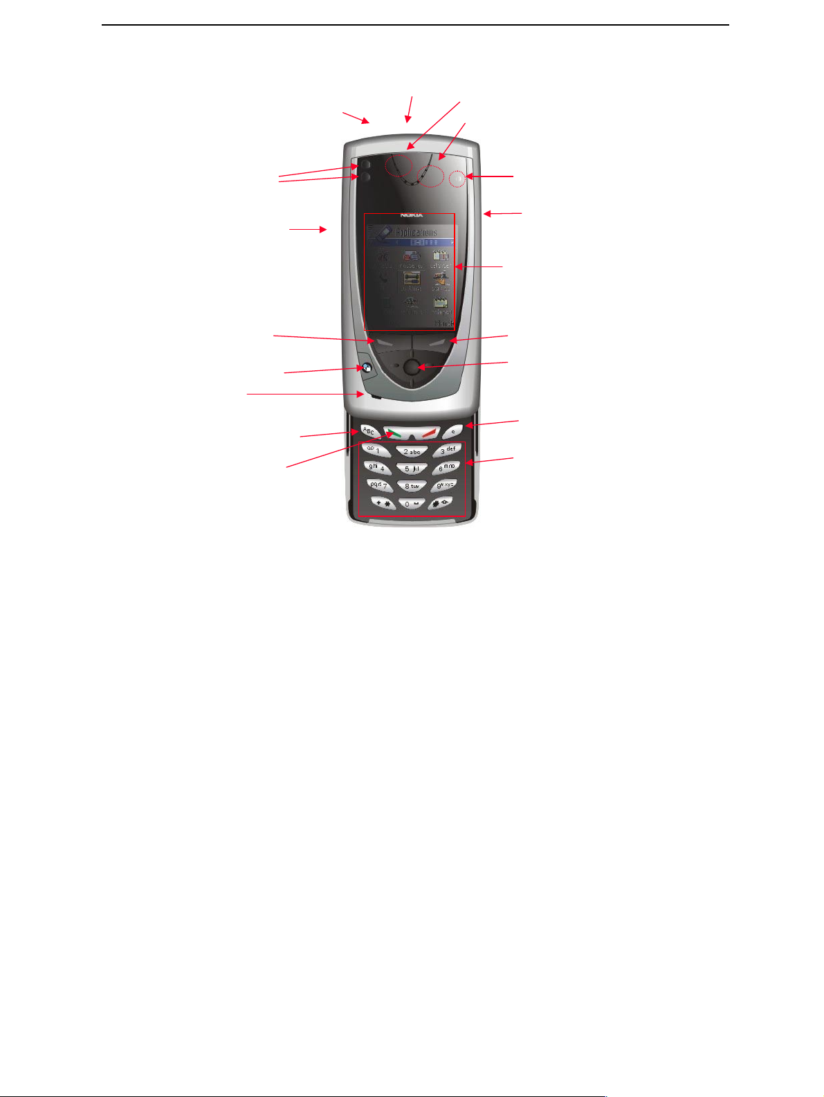
Figure 1: NHL-2NA user interface
Proximity sensor
Voice key
Left softkey
Apps key
Microphone
Shift key
Character input mode
Call creation key
Call termination key
SIM card
IrDa
Earpiece
IHF
Ambient light sensor
Power key
Display area
Right softkey
5-way joystick, “rocker”
(move up/down, arrow left/right,
selection key)
Clear key
Numeric keys
Issue 1 07/02 ¤Nokia Corporation Page 5
Page 6

User Interface CCS Technical Documentation
User Interface Module
UI Module comprises LCD, LCD drivers, LCD powering, LED backlightning, 5 way joystick,
transceiver keyboard and voice key.
Figure 2: UI module block diagram
Page 6 ¤Nokia Corporation Issue 1 07/02
Page 7

CCS Technical Documentation User Interface
I/O Terminals
Table 2: UI connector
Terminal No.
1VDD Power voltage I
2GND Ground I
3 D4 Command/data I/O terminal I/O
4 D0 Command/data I/O terminal I/O
5 A0 Command/data identification signal
6GND Ground I
7 VDDI Power voltage I
8 D1 Command/data I/O terminal I/O
9 D2 Command/data I/O terminal I/O
10 D3 Command/data I/O terminal I/O
11 Rocker3 5 way key I
12 Rocker2 5 way key I
13 GND-K 5 way key Ground I
Terminal
Name
Function I/O Remarks
I “L” command/”H” data
input
14 Rocker5 5 way key I
15 Rocker4 5 way key I
16 Rocker1 5 way key I
17 VLED+ LED positive I
18 VLED- LED negative I
19 Row1 Dome key I
20 Row0 Dome key I
21 Col1 Dome key I
22 Col0 Dome key I
23 GND Ground I
24 XRES Initial reset signal I “L” active
25 D5 Command/data I/O terminal I/O
26 D6 Command/data I/O terminal I/O
27 D7 Command/data I/O terminal I/O
28 GND Ground I
29 XRD Read signal I “L” active
30 XWR Write signal I “L” active
Issue 1 07/02 ¤Nokia Corporation Page 7
Page 8

User Interface CCS Technical Documentation
Figure 3: LCD Module
Absolute Maximum Ratings
Table 3: Absolute maximum ratings
Item Symbol Rating Unit Terminal
Power supply voltage V
Signal input voltage V
Signal output voltage V
LED input voltage V
Operating temperature range
Storage temperature
range
Note: values respect to UI module GND
DC Characteristics
UI connector is the connector between the UI module and NMP PWB.
DD 0 ~ +3.3 V VDD
V
DDI 0 ~ +3.3 V VDDI
IN 0 ~ VDDI+0.3 V D0~D7
OUT 0 ~ VDDI+0.5 V D0~D7, A0, XRES, XRD, XWR
LED 6 V Between VLED+ and VLED-
TOP -20 ~ 70 C No dew condensation
-30~-20 C No dew condensation
Reduced optical performance
T
ST -40 ~ 85 C No dew condensation
Table 4: UI-connector DC characteristics
Pin
no.
Signal
name
Type Min Typical Max Unit Description
1 VDD IN 2.6 2.78 2.9 V Voltage supply
2 GND 0 V System ground
3 D4 IN H: 0.7xVDDI
L: 0
OUT H: 0.8xVDDI
L: 0
H: VDDI
L: 0.3xVDDI
H: VDDI
L: 0.2 x VDDI
V Data to write
V Data to read
Page 8 ¤Nokia Corporation Issue 1 07/02
Page 9

CCS Technical Documentation User Interface
4 D0 IN H: 0.7xVDDI
L: 0
OUT H: 0.8xVDDI
L: 0
5 A0 IN H: 0.7xVDDI
L: 0
6 GND 0 V System ground
7 VDDI IN 1.65 1.8 1.95 V Logic voltage
8 D1 IN H: 0.7xVDDI
L: 0
OUT H: 0.8xVDDI
L: 0
9 D2 IN H: 0.7xVDDI
L: 0
OUT H: 0.8xVDDI
L: 0
10 D3 IN H: 0.7xVDDI
L: 0
H: VDDI
L: 0.3xVDDI
H: VDDI
L: 0.2 x VDDI
H: VDDI
L: 0.3xVDDI
H: VDDI
L: 0.3xVDDI
H: VDDI
L: 0.2 x VDDI
H: VDDI
L: 0.3xVDDI
H: VDDI
L: 0.2 x VDDI
H: VDDI
L: 0.3xVDDI
V Data to write
V Data to read
V H: data
L: command
supply
V Data to write
V Data to read
V Data to write
V Data to read
V Data to write
OUT H: 0.8xVDDI
L: 0
11 Rocker3 200 mOhm
12 Rocker2 200 mOhm
13 GND 0 V System ground
14 Rocker5 200 mOhm
15 Rocker4 200 mOhm
16 Rocker1 200 mOhm
17 V
18 V
19 Row1 IN/
20 Row0 IN/
+ IN/
LED
- IN/
LED
4.5 V LED, positive ter-
OUT
0 0 Vbat V LED, negative
OUT
OUT
OUT
H: VDDI
L: 0.2 x VDDI
1 Ohm Tracking resist-
1 mA Drive current
1 Ohm Tracking resist-
V Data to read
minal
terminal
ance
ance
1 mA Drive current
1 mA Drive current
Issue 1 07/02 ¤Nokia Corporation Page 9
Page 10

User Interface CCS Technical Documentation
21 Col1 IN/
OUT
22 Col0 IN/
OUT
23 GND 0 V System ground
24 RESX IN H: 0.7xVDDI
L: 0
25 D5 IN
OUT
26 D6 IN
OUT
27 D7 IN
OUT
H: 0.7xVDDI
L: 0
H: 0.8xVDDI
L: 0
H: 0.7xVDDI
L: 0
H: 0.8xVDDI
L: 0
H: 0.7xVDDI
L: 0
1 Ohm Tracking resist-
ance
1 mA Drive current
1 Ohm Tracking resist-
ance
1 mA Drive current
H: VDDI
L: 0.3xVDDI
H: VDDI
L: 0.3xVDDI
H: VDDI
L: 0.2 x VDDI
H: VDDI
L: 0.3xVDDI
H: VDDI
L: 0.2 x VDDI
H: VDDI
L: 0.3xVDDI
V Reset
(active low)
V Data to write
V Data to read
V Data to write
V Data to read
V Data to write
H: 0.8xVDDI
L: 0
28 GND 0 System ground
29 RDX IN H: 0.7xVDDI
L: 0
30 WRX IN H: 0.7xVDDI
L: 0
H: VDDI
L: 0.2 x VDDI
H: VDDI
L: 0.3xVDDI
H: VDDI
L: 0.3xVDDI
V Data to read
L: read
(active low)
L: Write
(active low)
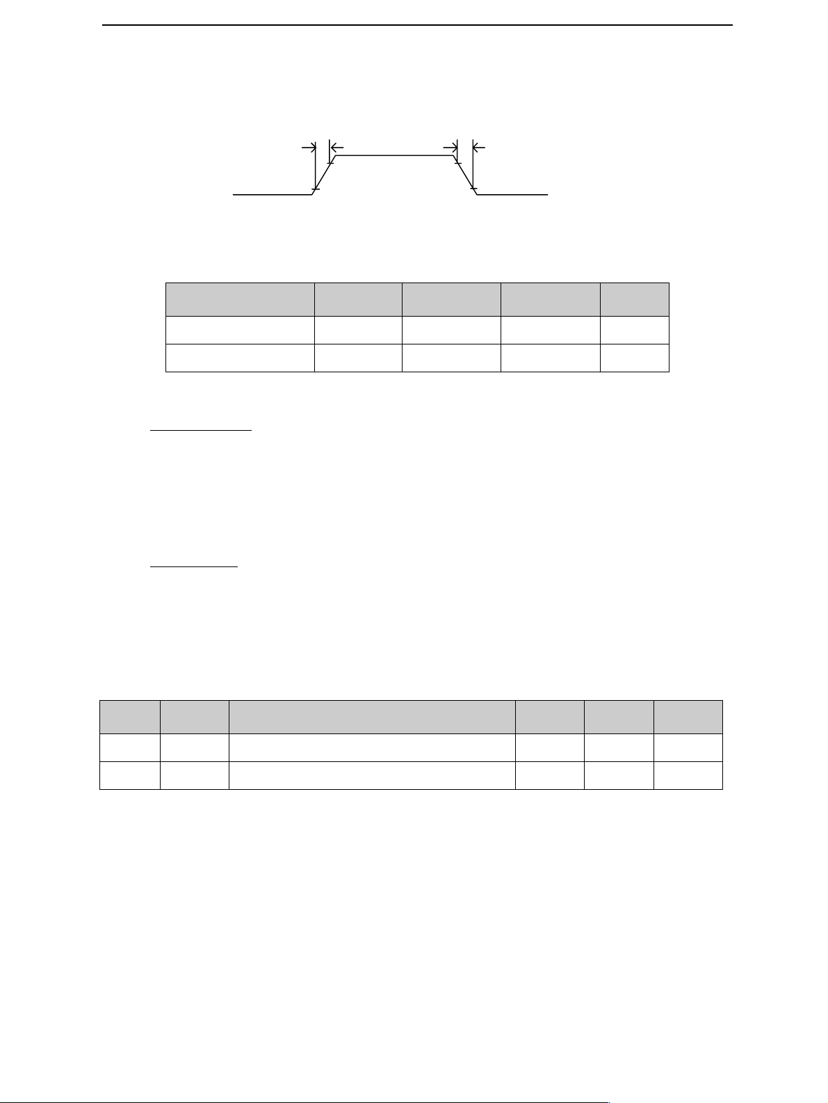
AC Characteristics of the Display
Signal timings are shown in Figure 7. Read/write characteristics and Table 10. AC characteristics. All the characteristics in this chapter are specified for the whole UI module,
including the UI-FPC.
Notes: Rise and fall time must be within 20 ns. Timings of T
ACC8
and T
are according
OH8
to 20% and 80% VDDI-GND. Other timings are according to 30% and 70% of VDDI-GND.
t
CCLW
and t
are specified according to overlapping of low level periods of CSX and
CCLR
WRX (RDX).
Definitions to rise and fall times as described in Figure 8. Rise and fall time in input and
output and Rise and fall times in input and output of display driver.
Page 10 ¤Nokia Corporation Issue 1 07/02
Page 11
CCS Technical Documentation User Interface
Figure 4: Rise and fall time in input and output
Table 5: Rise and fall times in input and output of display driver
Parameter Symbol Min Max Unit
Input tr, tf 20 ns
Output tr, tf 20 ns
Display Functional Specification
Displayed Data
Pixel and dot ordering in parallel transfer from engine to display is shown in Figure 9.
Pixel and dot order in transfer. Three bytes (RG, BR and BG) are needed to send data of
two pixels, as data of one pixel is 12 bits. Corresponding order in panel is shown in Figure
10. Pixel data order in display panel.
tr
70%
30%
tf
70%
30%
Reset Timing
Reset timing characteristics are shown in Figure 11. Reset timing and Reset timing. All
the characteristics in this chapter are specified for the whole UI module, including the
UI-FPC.
Table 6: Reset timing
Signal Symbol Parameter Min Max Unit
RESX TRW Reset pulse duration 200 ns
TRT Reset cancel 1200 ns
Issue 1 07/02 ¤Nokia Corporation Page 11
Page 12

User Interface CCS Technical Documentation
Transceiver keyboard
The transceiver keyboard Interface requires 4 programmable I/O pins. The transceiver
keyboard interface can be connected to Nokia Engine with these 2 + 2 I/O-pins. T
Key Description
Key1 Left_Soft_Key
Key2 Right_Soft_Key
Key3 Apps Key
Key4 Side Key
Rocker key
The rocker key is a replaceable part.
Rocker interface
Rocker is connected to general purpose IOs that have internal pull ups. Pull up voltage is
1.8V.
Figure 5: Electrical interface of the rocker
Rocker
UI Connector
Rocker1
Rocker2
Rocker3
Rocker4
Rocker5
ESD GND
GND
UI Module
Rocker is operated as a switch in an ideal case. In reality more than two pins can be
connected to ground with one move.
Page 12 ¤Nokia Corporation Issue 1 07/02
Page 13

CCS Technical Documentation User Interface
Figure 6: Rocker switch 2
Table 7: Switching order of the terminals
Leaning
direction
A * *
B * *
C * *
D * *
Center
push
Terminal number
1 2 3 4 5 Com
* *
Issue 1 07/02 ¤Nokia Corporation Page 13
Page 14
User Interface CCS Technical Documentation
V
j
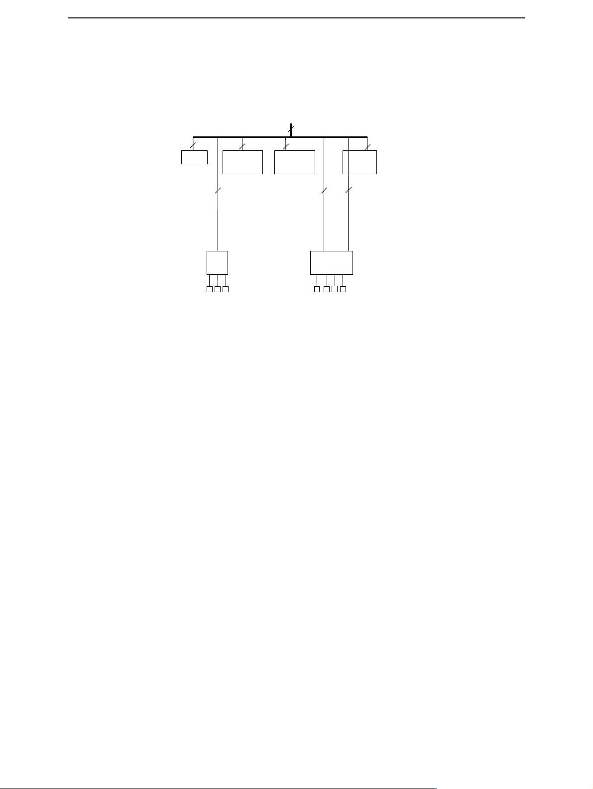
Grip module
Grip module includes the keyboard with its PWB and backlight, the vibrator.
Battery is also included in this module
Figure 7: Grip module.
18
1
ibra Keyboard
16 keys
8
1
Backlight
8 LED’s
2
Current
Gauge
DC-
ack
2
Battery
connector
1
3
Page 14 ¤Nokia Corporation Issue 1 07/02
 Loading...