

Page 1

NHL-2NA Series Transceivers
Camera Module
Issue 2 11/02 ¤Nokia Corporation
Page 2

Camera Module CCS Technical Documentation
[This page left intentionally blank]
Page 2 ¤Nokia Corporation Issue 2 11/02
Page 3

CCS Technical Documentation Camera Module
Table of Contents
Page No
Abbreviations ...............................................................................................................4
Camera Module.............................................................................................................. 5
Key specification .........................................................................................................5
Electrical specifications ...............................................................................................5
Block diagram........................................................................................................... 5
Signal description...................................................................................................... 6
DC characteristics ..................................................................................................... 7
Signals specifications ...................................................................................................8
Signals and timing..................................................................................................... 8
Synchronization......................................................................................................... 8
Sub LVDS specification............................................................................................ 8
Camera control interface ............................................................................................10
General .................................................................................................................... 10
Operating procedure ..................................................................................................10
Mode description..................................................................................................... 10
Operation flow chart................................................................................................ 10
Mechanics ..................................................................................................................11
List of Figures
Fig 1 Block diagram of camera module...............................................................................6
Fig 2 CCP interface between camera and engine ................................................................8
Fig 3 sub LVDS configuration.............................................................................................9
Fig 4 Top view.....................................................................................................................12
Issue 2 11/02 ¤Nokia Corporation Page 3
Page 4

Camera Module CCS Technical Documentation
Abbreviations
VGA Video Graphic Array
CIF Common intermediate format
CCI Camera Control Interface
LVDS Low voltage differential signals
CCP Compact camera port
CDS Correlated double sampling
AGC Automatic gain control
ADC Analog digital converter
TG Timing generator
SG Synchronization generator
PLL Phase locked loop
VCO Voltage control oscillator
AWB Automatic white balance
AES Automatic electronics shutter
Page 4 ¤Nokia Corporation Issue 2 11/02
Page 5
CCS Technical Documentation Camera Module
5
3
Camera Module
Key specification
The table below shows the key specification of the VGA2 camera module (TCM8002MD).
Table 1: Key specification
Array format active: 660 H x 492 V
Image sensor
color filter RGB bayer arrangement
Optical format 1/4 "
pixel size 5.4 um
F no. 2.8
degrees(H) / 39(V) / 65(D)
30 cm to infinity
lens
H view angle
focal length 3.5 mm
focus range
focus adjustment Object distance for adjustment is infinity.
image signal output CCP ( sub LVDS serial output)
output image format YUV 4:2:2, RGB 5:6:5, sensor 10 bit raw data
image size A variety of size is supported. See table 6
Interface
frame rate typical : 15 fps
master clock External clock is supplied.
control interface CCI bus
mechanics 13-pin spring connector
Power source
Current consumption
Dimension
VDD=DC 2.78 +/- 0.13 V and VDDI =DC 1.8 +/- 0.1
VDD on & VDDI
VDD off & VDDI
16 mm (H) x 20 mm ( W) x 8.9 mm (D) excluding protrusion of connector
34 mA typical for VDD, 7 mA typical for VDDI
1uA
Weight 1.6 gram
operation -30 to + 70 centigrade
Temperature range
full quality
-10 to + 40 centigrade
storage -40 to + 85 centigrade
infinity
VDDI
Electrical specifications
Block diagram
The figure below shows the block diagram of the VGA2 camera module connected to
Nokia Engine.
Issue 2 11/02 ¤Nokia Corporation Page 5
Page 6

Camera Module CCS Technical Documentation
V
Figure 1: Block diagram of camera module
Single lens
VGA CMOS sensor Camera DSP
Image
Section
TG
2
CDS/AGC
ADC
Spring connector
GA2 Camera Module
Signal
Processing
SG
CCI bus
I/F
2
0.01
uF
Nokia Engine
Format
Converter
Sub LVDSPLL/VCO
43
Signal description
The following description indicates the meaning of each signal shown in figure above.
(1) VDD Supply voltage to the main circuits of a camera module
(2) GND2 Ground line corresponding to VDD
(3) D + Fast serial data out
(4) VDDI Supply voltage to sub LVDS circuit. This voltage can be always applied,
(5) D - Fast serial data out of which is inverted to D+
(6) SDA Serial data line of CCI bus
(7) GND1 Ground line corresponding to VDDI
(8) SCL Serial clock line of CCI bus
(9) Clk + Fast serial clock
(10) Vctrl This signal is used for sub LVDS circuit to be shut off in order to reduce
(11) Clk - Fast serial data out of which is inverted to Clk+
(12) GND3 Ground line corresponding to Extclk.
(13) Extclk System clock from Nokia engine to the camera module. This signal is
even if the Vctrl is off.
stand-by current of a camera module. “High” designates “ON”. Please
see the operation flow chart.
sinusoidal by RC filtering on Nokia engine. Extclk is AC coupled to the
camera module through a capacitor of which capacitance is more than
Page 6 ¤Nokia Corporation Issue 2 11/02
Page 7

CCS Technical Documentation Camera Module
0.01 uF. Extclk has 4 operating modes depending on the wireless system
in which the camera module is used. The Extclk is active before VDD is
on. This Extclk shall be exclusively used for generating any other clocks
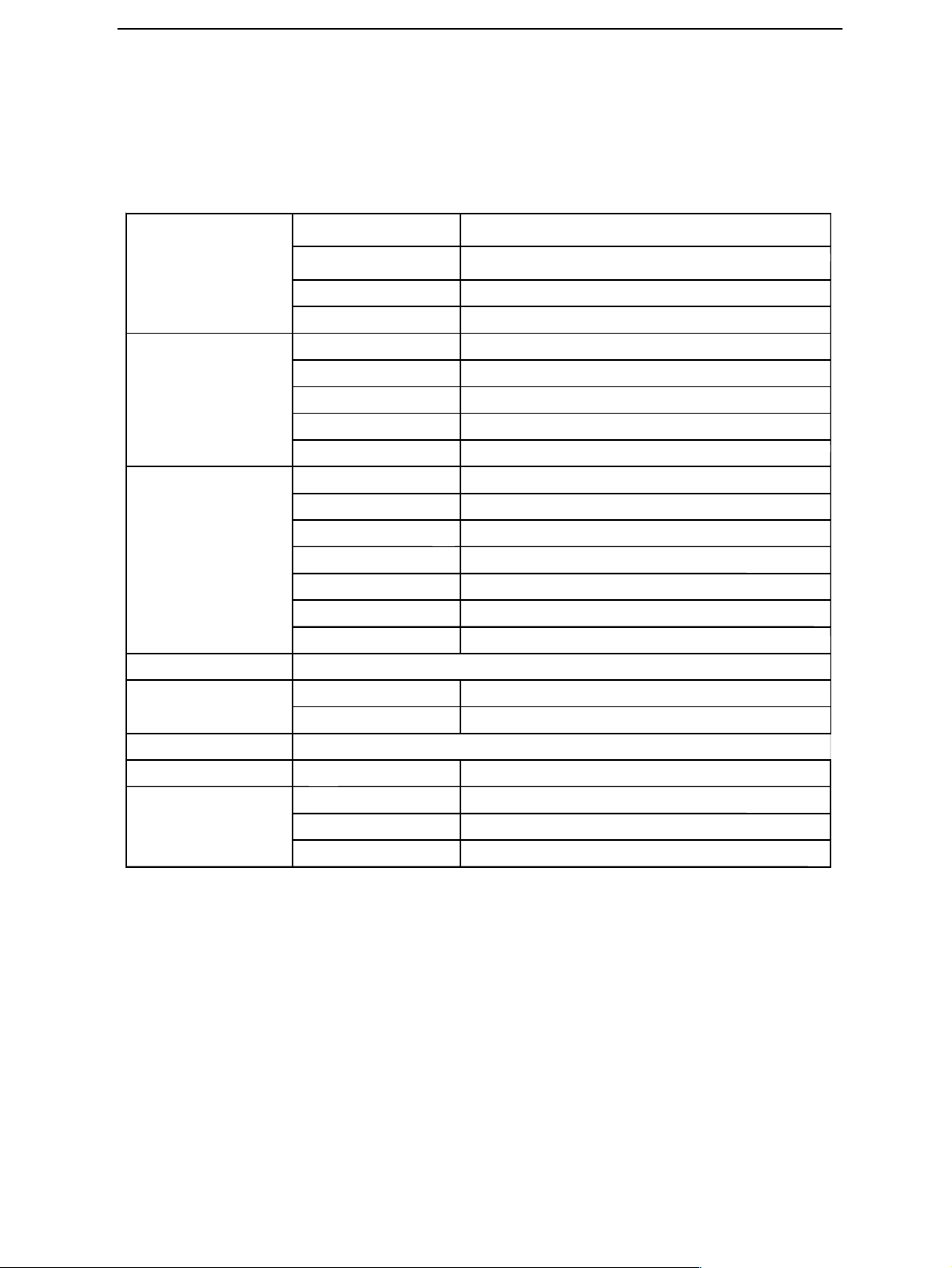
DC characteristics
(1) Maximum ratings
VDD 3.6 V
VDDI 2.7 V
Input signals, min -0.3 V
Input signals, max VDDI (1.8V) + 0.3 V
Note: Values respect to GND.
(2) DC characteristics of each signal are shown in the table below.
Table 2: DC characteristics of each signal
Issue 2 11/02 ¤Nokia Corporation Page 7
Page 8

Camera Module CCS Technical Documentation
Signals specifications
Signals and timing
The fast serial interface of digital image data is employed for the VGA camera module.
The fast serial interface described in this document is named CCP (Compact Camera
Port). In terms of signaling scheme, CCP is based on the idea of IEEE standard LVDS signaling scheme (current mode differential low voltage signaling method). CCP described
in this document utilizes lower voltage than that of standard LVDS. The low voltage LVDS
is named in this document sub LVDS. CCP is an one-way differential serial camera connection with clock and integrated line / frame synchronization:
Figure 2: CCP interface between camera and engine
Camera Engine
D+
D-
D+ and D- are differential picture data output from the camera module. This data is
written on each falling edge of Clk. Data format is least significant bit first. When nothing is being transferred, D remains high, except in power shut-down.
Clk+ and Clk- are differential pixel clock. Data should be read by the receiving end on
rising edge. When nothing is being transferred, Clk remains high, except in power shutdown.
Synchronization
Each image line that is received begins with line synchronization code and ends with line
end code. Each frame begins with frame synchronization code and ends with frame end
code. At frame start and frame end no line synchronization are added but they are
replaced by the frame synchronization.
Sub LVDS specification
General
Clk+
Clk-
The fast serial transfer of image data from the camera module to Nokia engine is to be
achieved based on 1.8 power supply condition. Accordingly, modified LVDS type current
mode transmitters/receivers is used. In this document, the LVDS scheme which is modified corresponding to 1.8 V is named sub LVDS. The figure below shows simplified configuration of sub LVDS
Page 8 ¤Nokia Corporation Issue 2 11/02
Page 9

CCS Technical Documentation Camera Module
Figure 3: sub LVDS configuration
1.8V typ
D+
D-
Camera module Nokia engine
100R
DC, AC characteristics
DC characteristics, AC characteristics (transmitting end) and (receiving end) are shown in
the tables below.
Table 3: DC characteristics
Item Min Typ Max
Bus operating voltage
1.7 1.8 1.9
Absolute maximum rating -0.3
VDDI +
Unit
V
V
Table 4: AC characteristics of camera module
Parameter Signal level
Min Typical Max
Input voltage range VDDI/2-0.1 VDDI/2 VDDI/2+0.1 V
Differential voltage swing Vod 100 150 200 mV
Output impedance R0 40 100 140 Ohm
Operating frequency 1 120 MHz
Clock duty cycle @ 120 MHz 40 50 60 %
Vod rise time 20% - 80% 300 500 ps
Vod fall time 80% - 20% 300 500 ps
Note: Vod is measured with 100 ohm termination.
Issue 2 11/02 ¤Nokia Corporation Page 9
Page 10

Camera Module CCS Technical Documentation
Camera control interface
General
The camera control interface configuration is based on fast mode IIC(i.e. I
Slave address
The Camera Module control interface has got slave address 78h. General call address and
start byte are not supported.
Sub address
A sub address for internal register are prepared. Width of sub address is 8 bits, and each
address has 8 registers. The camera module has the function of increment addressing,
the host can operate continuous addresses by one sequence. After system reset by Power
ON (when VDD is applied) subaddress becomes 00’h.
Read & write
2
C) bus.
Nokia engine can read and write all registers’ data except for test registers.
Operating procedure
Mode description
This camera module supports following two operating modes.
1 Normal mode
This mode means continuous image capturing operation.
(Namely every frame is output.)
2 Long storage mode
This mode means intermittent image capture operation (one frame out of every
four frame) particularly in case of long time exposure. Nokia engine submits a
command to set this mode.
Operation flow chart
(1) For Power-on, the following order is necessary.
VDDI(1.8 V) power ON Extclk ON Vctrl ON VDD(2.8 V) Power ON
T1 T2 T3 T4
Command for initializing Image data output start.
T5
In the figure below, “VD” is internal synchronization pulse to show vertical scanning
period.
Page 10 ¤Nokia Corporation Issue 2 11/02
Page 11

CCS Technical Documentation Camera Module
T
m
u
s
T
Figure 9. operation sequence in power-on
VDDI
T1>=0 msec
Extclk
T2>=0 msec
Vctrl
T3 >=10 msec
VDD
4>=40msec
first IIC command
VD
VCO
firstoutput frame
(2) For Power-off
VDD(VDD2.8 V) Vctrl OFF Extclk OFF OFF VDDI (1.8 V) OFF
T1>=0 T2>=0 T3>=0
Mechanics
The camera module has got a plastic lens holder with a metallized surface. The lens barrel part does not have metallization. The material of the lens holder plastic is 30% metal
coated carbon. The lens barrel material is non-conductive carbon. The lens holder has a
curved rib for attaching the module into the mobile phone. The connector is the spring
type. The PWB material is FR4.
ax : 273msecmax : 80 msec
nstable
5=353 msec
table
Pin assignment is shown in Figure 9 and Table 9.
Issue 2 11/02 ¤Nokia Corporation Page 11
Page 12

Camera Module CCS Technical Documentation
Figure 4: Top view
Spring connector(top view)
13
11
Lens Holder
The position
of sensor
pixel (1,1)
PCB
Table 5: Pin assignment
Pin number 1 2 3 4 5 6 7 8
Pin name VDD GND2 D+ VDDI D- SDA GND1 SCL
11
9
7
5
3
1
12
10
8
6
5
4
3
2
1
12
10
9
8
7
6
4
2
Pin number 9 10 11 12 13
Pin name CLK+ Vctrl CLK- GND3 EXTCLK
Page 12 ¤Nokia Corporation Issue 2 11/02
Page 13

CCS Technical Documentation Camera Module
This page intentionally left blank.
Issue 2 11/02 ¤Nokia Corporation Page 13
Page 14

Camera Module CCS Technical Documentation
Page 14 ¤Nokia Corporation Issue 2 11/02
 Loading...