

Page 1

NHL-2NA Series Transceiver
Troubleshooting Instructions
Issue 2 11/02 Copyright ¤Nokia. All rights reserved
Page 2

Troubleshooting Instructions CCS Technical Documentation
[This page left intentionally blank]
Page 2 Copyright ¤Nokia. All rights reserved. Issue 2 11/02
Page 3

CCS Technical Documentation
Table of Contents
Baseband Troubleshooting............................................................................................. 3
Introduction ..................................................................................................................3
General guidelines for NHL-2NA system troubleshooting .........................................3
Troubleshooting paths .................................................................................................6
LG4 Baseband HW subarea troubleshooting ............................................................10
Energy management troubleshooting ........................................................................12
IR interface ................................................................................................................24
Sensors troubleshooting .............................................................................................26
Proximity Detector .....................................................................................................27
Ambient Light Detector .............................................................................................33
SIM card ....................................................................................................................39
Audio .........................................................................................................................43
Memory troubleshooting ...........................................................................................47
Baseband serial interface troubleshooting .................................................................48
Hall sensor troubleshooting .......................................................................................51
Display backlights troubleshooting ...........................................................................52
Bluetooth troubleshooting .........................................................................................53
Needed actions if ASIC is changed.............................................................................. 56
UEM changed ............................................................................................................56
AEM changed ............................................................................................................56
UPP_WD2 changed ...................................................................................................56
Flash0 changed ..........................................................................................................56
RF component changed .............................................................................................56
Test points and pin orders............................................................................................ 57
Test points in BaseBand area (LG4_06_02) ..............................................................57
Connectors pin order ..................................................................................................59
RF Troubleshooting ..................................................................................................... 63
Introduction ................................................................................................................63
RF Key component placement ...................................................................................64
Fault finding test point locations ...............................................................................65
Receiver .....................................................................................................................66
Transmitter .................................................................................................................73
Common ....................................................................................................................79
Receiver tunings ........................................................................................................85
Transmitter Tunings .................................................................................................100
Appendix.................................................................................................................... 108
Frequency mappings ................................................................................................108
UI Troubleshooting.................................................................................................... 117
Introduction ..............................................................................................................117
UI module troubleshooting cases .............................................................................117
Grip-Module Troubleshooting................................................................................... 121
Introduction ..............................................................................................................121
Backlight ..................................................................................................................122
Current Gauge ..........................................................................................................123
Vibra ........................................................................................................................124
Keyboard ..................................................................................................................125
Hall Sensor ...............................................................................................................126
Issue 2 11/02 ¤Nokia Corporation Page 1
Page 4

CCS Technical Documentation
Camera Troubleshooting Instructions........................................................................ 127
Background, tools and terminology .........................................................................127
Image taking conditions effect to image quality ......................................................128
Camera construction ................................................................................................134
Image quality analysis .............................................................................................135
Fault finding trees ....................................................................................................141
Page 2 ¤Nokia Corporation Issue 2 11/02
Page 5

CCS Technical Documentation
Baseband Troubleshooting
Introduction
This document is intended to be a guide for localising and repairing electrical faults in
the NHL-2NA device. First there is a brief guide for fault localising. Then fault repairing is
divided into troubleshooting paths.
Before any service operation you must be familiar with the NHL-2NA product and module level architecture. You also have to be familiar with the NHL-2NA specified service
tools such as the Phoenix service software, flashing tools and software.
General guidelines for NHL-2NA system troubleshooting
Tools needed for troubleshooting
• Service tools (as listed at service tools chapter in service manual)
• Laboratory power supply with current indicator
• Oscilloscope
• Digital multimeter
General guidelines
General notes about the NHL-2NA product:
• Large colour display
• Keyboard on grip part, rocker, two softkeys and application key under display +
side keys (power key and IHF enabling key)
• Flex cable carries signals between LG4 and LS4 boards. Battery and charger plug
is in grip part, so if the flex is damaged phone cannot be powered on.
• UI-module (display, backlights etc.) is also connected to LG4 module with flex
cable.
• If the component reference is under 100, component is located at the LS4 board.
And if the component reference is over 100, component is located at the LG4
board.
When you get a faulty NHL-2NA device and you start to troubleshoot it, first check the
following items:
• If the device cannot be turned on by any means, see “dead device” troubleshooting
• Current consumption (missing consumption) gives an idea wether the device is
able to start up.
• Dropping supply voltage or very large current consumption indicates a short circuit
• Check wether the connection with Phoenix works and what can be discovered
with Phoenix (ADC-readings, baseband selftest, bb-calibrations etc.)
• Check baseband selftests with Phoenix if “CONTACT THE RETAILER.” is shown on
the display.
• Check visually display and rocker faults
• Force phone to LOCAL mode and make keyboard test by phoenix
Issue 2 11/02 ¤Nokia Corporation Page 3
Page 6

CCS Technical Documentation
• Check that board-to-board connector, hotbar and adapter connections are OK,
and connectors make good contacts.
• If liquid damage, stop repairing!
If some module (eg. Camera, display, grip) is not working:
• Try working module
If this not helping
• Check supply voltages for failed module
• Check clock(s) for failed module
=> Go to relevant chapter of this document
Flash phone before disassembling it if fault is not obvious and Phoenix connection is
OK.
Dissasemble phone:
Try to locate failed module, is it LG4, LS4, UI or camera module.
• Check failed module visually:
Mechanical damages?
Solder joints OK?
Continue with specific troubleshooting procedure for the module:
• If there is an obvious fault, repair it before reflashing the device
• Flash first if a fault is not obvious
If flashing is not working go to flashing troubleshooting
Due to CSP packages short circuits or broken solder joints are not easily seen. If the
examined signal seems to be continuously in low or high level, then measure for possible
short circuit to ground (signal low) or to supply voltage (signal high) Note that if a problem is not found from any visible contact/component it can be under CSPs where the signal is connected.
Care must be taken when assembling and disassembling the tranceiver. Failure to do this
may result in unnecessary damage to device.
NOTE! if some ASIC is changed see chapter Bluetooth troubleshooting
Nominal current consumption
NOTE: Service tools need some amount of current to work. (FLA-21: 1-2mA and MJF-9Q:
2-6mA
Page 4 ¤Nokia Corporation Issue 2 11/02
Page 7

CCS Technical Documentation
The following current consumption values are measured from a complete NHL-2NA.
Vbatt = 3.8 – 4.2V
Measured nominal currents are drawn from the main battery.
Measurements have been made with a current probe connected to an oscilloscope.
Operating mode
Idle (BT off) 4-8 mA
2w audio call (backlights off) channel37 300-340mA
Viewfinder + nominal backlights 232mA
Current consumption
Issue 2 11/02 ¤Nokia Corporation Page 5
Page 8
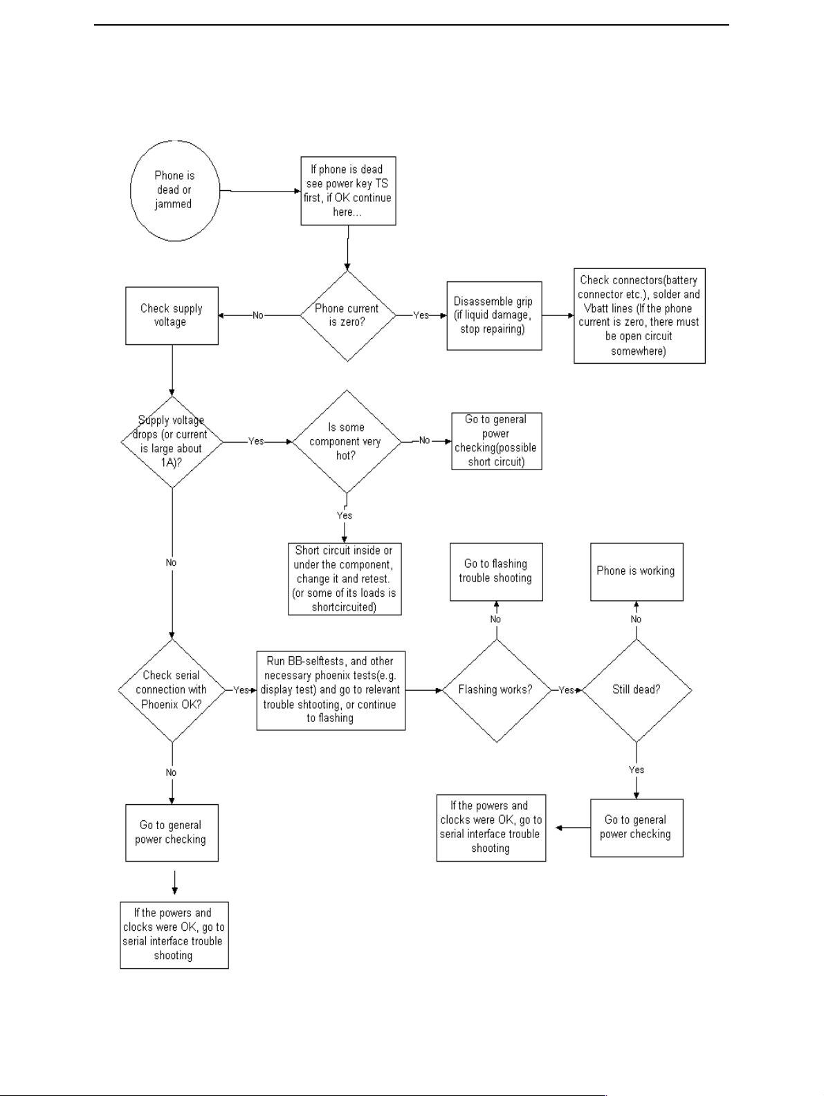
Troubleshooting paths
Dead or jammed device
CCS Technical Documentation
Page 6 ¤Nokia Corporation Issue 2 11/02
Page 9

CCS Technical Documentation
Partially damaged device
If the device is working, but some functionality is missing try to localize where the problem is and see relevant part of this manual. If, for example, audio is not working see
chapter Audio Troubleshooting, if charging is not working see chapter Charging Troubleshooting, etc.
Most common symptoms reported by customer
In this section is described most common symptoms reported by customers when the
device is brought to service. Some tips where the trouble can be found are also given.
When troubleshooting use these tips and follow the given troubleshooting path.
Most common symtoms for audio problems can be:
“Earpice sound is missing”
”Handsfree sound is missing”
”Headset is not recognized”
”Microphone is not working”
”Volume cannot be adjusted”
” Ringing tones do not work”
”Audio volume too low”
If symptom is something like above see audio troubleshooting.
Most common symptoms for Irda and bluetooth problems can be:
“Irda does not work or it does not make a connection”
”Bluetooth does not work or connection cannot be established”
If symptoms are something like those, start to follow Irda or bluetooth
troubleshooting guidelines gave relevant chapters.
Symptoms related to energy management:
“Phone does not stay on”
”Charging is not working”
”Time is lost during battery change or short main battery removal”
”Charging takes too long”
”Operating time is very short”
These symptoms lead to relevant part of energy managemant troubleshooting
If the sensor/sensors are out of order description of symptoms can be like below:
“IHF is not disabled automatically when phone is put near ear”
“IHF cannot be enabled”
“Backlight is always ON or OFF”
“Backlight of display does not go OFF”
Issue 2 11/02 ¤Nokia Corporation Page 7
Page 10

In cases above see Chapter Sensors Troubleshooting or Backlight Troubleshooting
Problems in UI-module:
“UI-module keypad is not working”
”Joystick is not working”
”Backlight is dim”
”Baclight not even”
”Backlight is blinking”
”Keypad or display backlight is not working”
”Display related problems”
See UI- module troubleshooting.
Most common RF related symptoms:
“Call cannot be made”
”Phone does not find signal”
”Call is often dropped”
CCS Technical Documentation
See RF troubleshooting
Problems with camera can cause symptoms as:
“Bad image quality”
”Picture cannot be taken”
See camera module troubleshooting
Problems in LS4 can cause symptoms below:
”Backlight of grip is dim”
”Baclight of grip not even”
”Backlight of grip is blinking”
”Grip keypad is not working”
”Vibra is not working or is noisy etc.”
See grip- module troubleshooting.
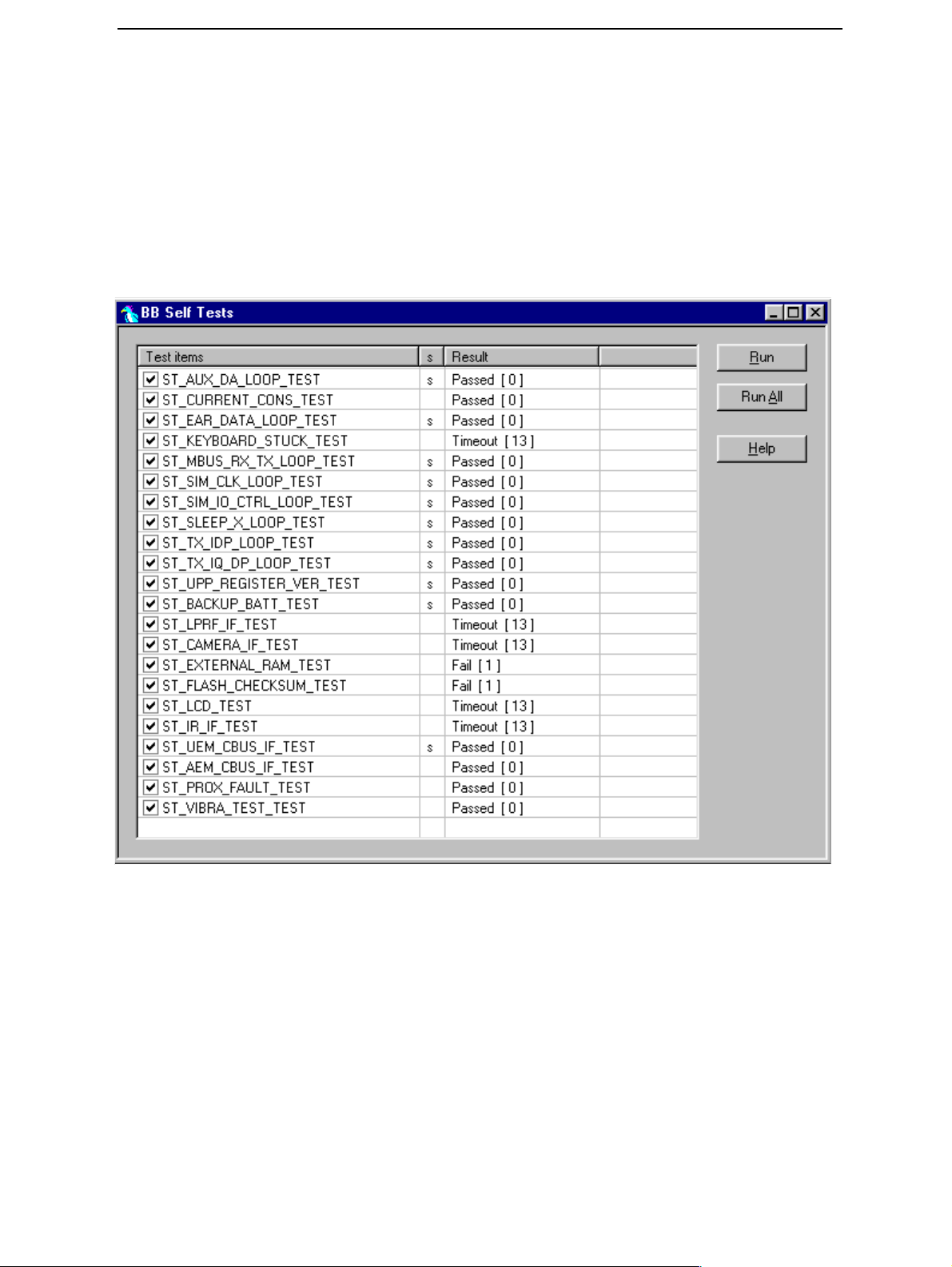
Contact the retailer” on display
“Contact the retailer.” on display (Self-tests by Phoenix)
Display information: “Contact the retailer”
Page 8 ¤Nokia Corporation Issue 2 11/02
Page 11
CCS Technical Documentation
This fault means that software is able to run and thus the watchdog of UEM can be
served.
Selftest functions are executed when the phone is powered on and if one or more selftest functions fail, the message “Contact the retailer” is shown on the display.
MCU selftest cases can be split into two categories: The ones that are executed during
power up and the ones that are executed only with a PC connected. These tests and the
items included are as follows:
Figure 1: BB selftest-tool
If a selftest fails, see relevant chapter in this troubleshooting manual.
Issue 2 11/02 ¤Nokia Corporation Page 9
Page 12
LG4 Baseband HW subarea troubleshooting
B
C
Flashing troubleshooting
NHL-2NA has three memory components installed on the main pwb. The best indication
of which one is causing problems can be obtained by flashing the device. It has to be
kept in mind that all three memory components are interfaced with UPP WD2 asic that
might itself have some problems. The necessary steps are described below. Phoenix error
messages during flashing greatly help on defining what is wrong. To be able to flash the
device, most device BB area components must function properly.
Flashing
faults
CCS Technical Documentation
C101 "Boot
timeout" or
C102 "boot start
txd fail"
message
?
No
C103
"Boot serial line
fail" message
?
No
C106
"Secondary
receive fail"
message
?
Yes
Yes
Yes
Measure BSI
pulse during
flash
programming
Is it ok?
Yes
Measure
I_FBUS_TX(J121)
line during flash
programming is it
1.8V?
Yes
No
Check connections
Check BB voltages
heck clocks
Check BSI line
attery connector, flex,
C239, Z383, R384
Change
UEM(D190)
No
Change UPP
WD2(D100)
No
Change UEM(D190)
Change
UPP_WD2(D100)
No
C202
"Algorithm
send" or C281
"phone message
chksum" fail
?
No
Sleep
clock(J101) ok ?
Yes
Yes
Flashing
faults page
2
Page 10 ¤Nokia Corporation Issue 2 11/02
Page 13
CCS Technical Documentation
C
Flashing
faults page
2
No
C108
"Prommer
message about
sdram failure"
?
No
Yes and sdram
allready changed
Yes
No
Activity in sdram
clk(J108) pad?
Yes
Change
UPP_WD2(D100)
Change
SDRAM(D312)
A204
"Wrong
manufacturer ID
and device ID"
message
?
No
C385
"Data block
handling timeout"
message
?
No
C586
"Phone fail
responce" or C684
"Data blok Nak"
message
?
Yes
Yes
Yes
hange Flash Chip according
to Phoenix messages
If both chips report wrong
ID's -> change
UPP_WD2(D100)
Bluetooth module is unable to start
flashing ->
Check V590,R591,R593-596,C594
and C595 -> still not ok
-> change BT module
Check flash0 bypass caps, check
Vpp connection to flasher, Check
R314(4.7k)
Ok->Change flash0(D311)
No
Flashing
successful/Retest
Issue 2 11/02 ¤Nokia Corporation Page 11
Page 14

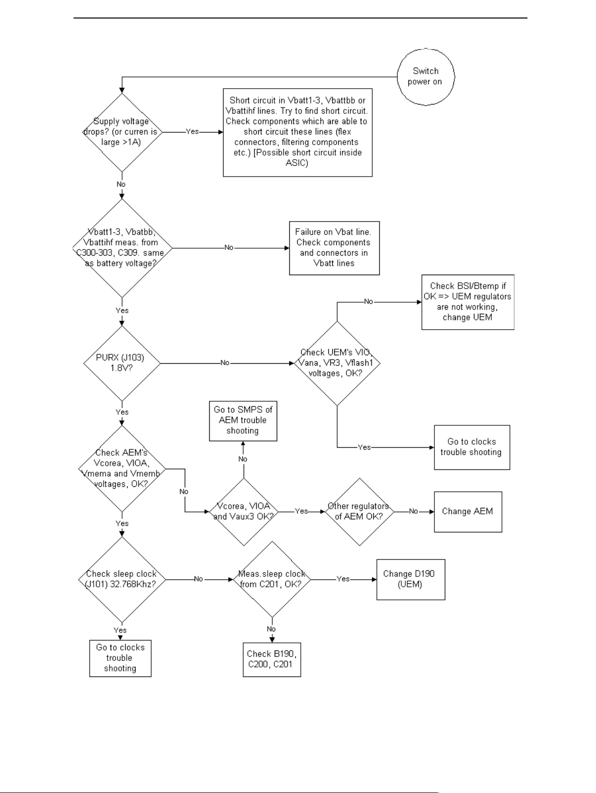
Energy management troubleshooting
Device does not stay on
If the device is switched off without any visible reason, there may be problems in the following areas:
• UEM watchdog problem (WD is not updated by SW)
• BSI line problem (BSI line is floating => contact failure)
• Battery line problem
• Soldering problem
The most likely reason is UEM WD (watchdog), which turns the device off after about 32
seconds if SW is jammed.
This may be caused by a SW problem, UPP_WD2 problem (Not server by SW), UEM, AEM
or memory malfunctions.
The following tests are recommended:
CCS Technical Documentation
• General power checking
•Clocks
•Memory testing
• Serial Interface
If there is something wrong in BSI line, the device seems to be dead after the power key
is pressed. However the regulators of the device are on a few seconds before the powerdown.
This mode can easily be detected from the current consumption of the device. After a
few seconds the current consumption drops almost to 0 mA.
In this case check components listed below or soldering:
Battery connector X002
Grip connector X001 (especially pin number 27)
Hotbar soldering X380 (especially pin number 5)
EMI-filter Z383 (especially pins number A4 and E4)
UEM D190 (pin number C2)
If phone boots to TEST or LOCAL mode with normal battery, BSI or Btemp or both lines
are short circuited to ground. Check varistors, EMI-filter and filtering capacitors, which
are located to BSI and Btemp lines.
General power checking
Use service tool FLA-21. Battery voltage should be atleast 3.6V. After phone disassembly,
use module jig MJS-9Q.
Page 12 ¤Nokia Corporation Issue 2 11/02
Page 15
CCS Technical Documentation
.
Issue 2 11/02 ¤Nokia Corporation Page 13
Page 16
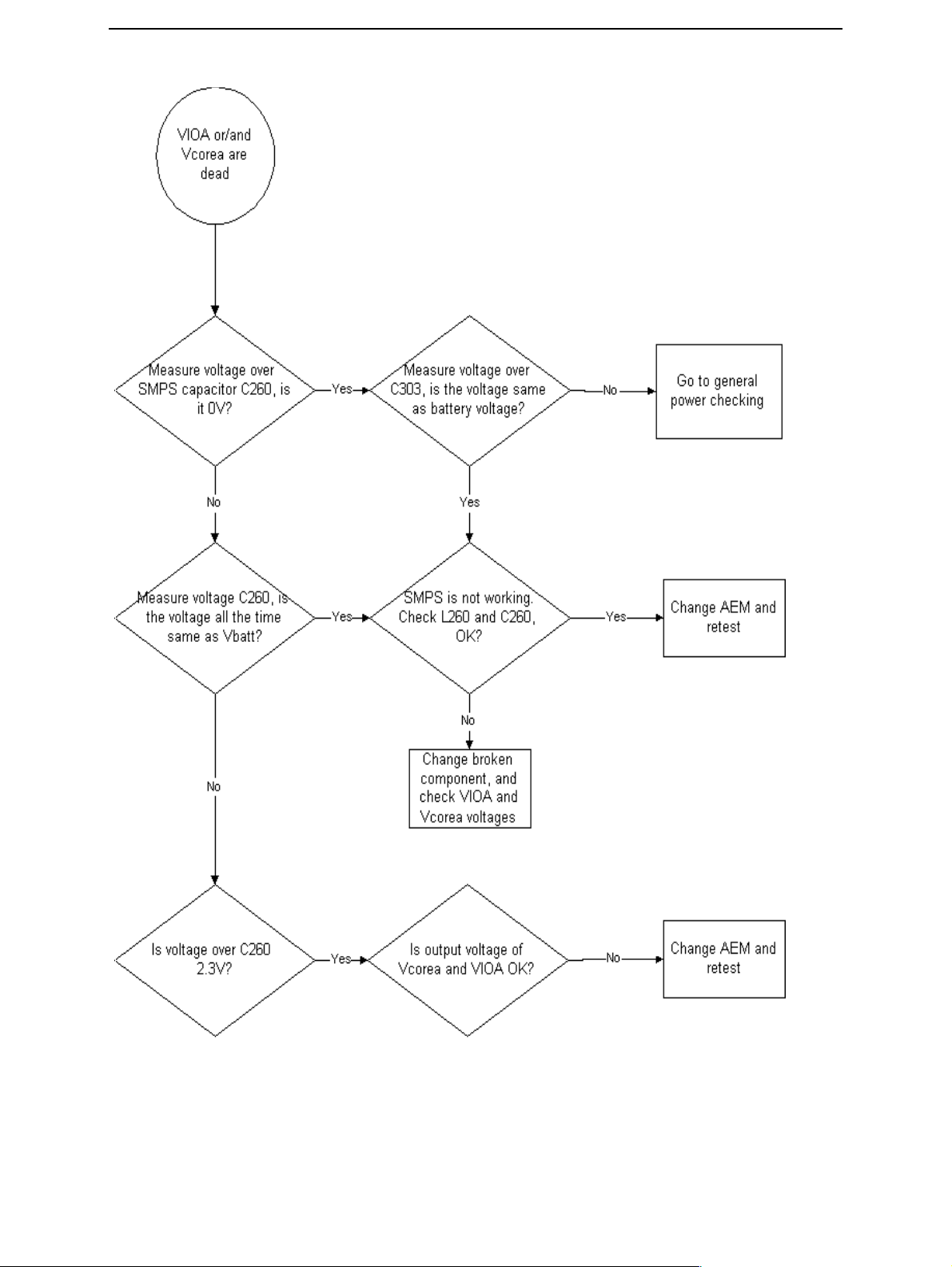
SMPS of AEM troubleshooting
CCS Technical Documentation
Page 14 ¤Nokia Corporation Issue 2 11/02
Page 17
CCS Technical Documentation
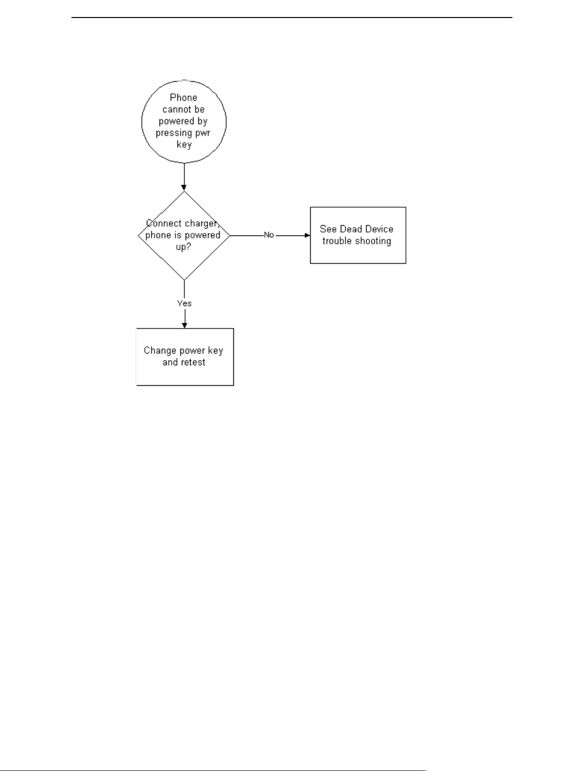
Power key troubleshooting
Issue 2 11/02 ¤Nokia Corporation Page 15
Page 18
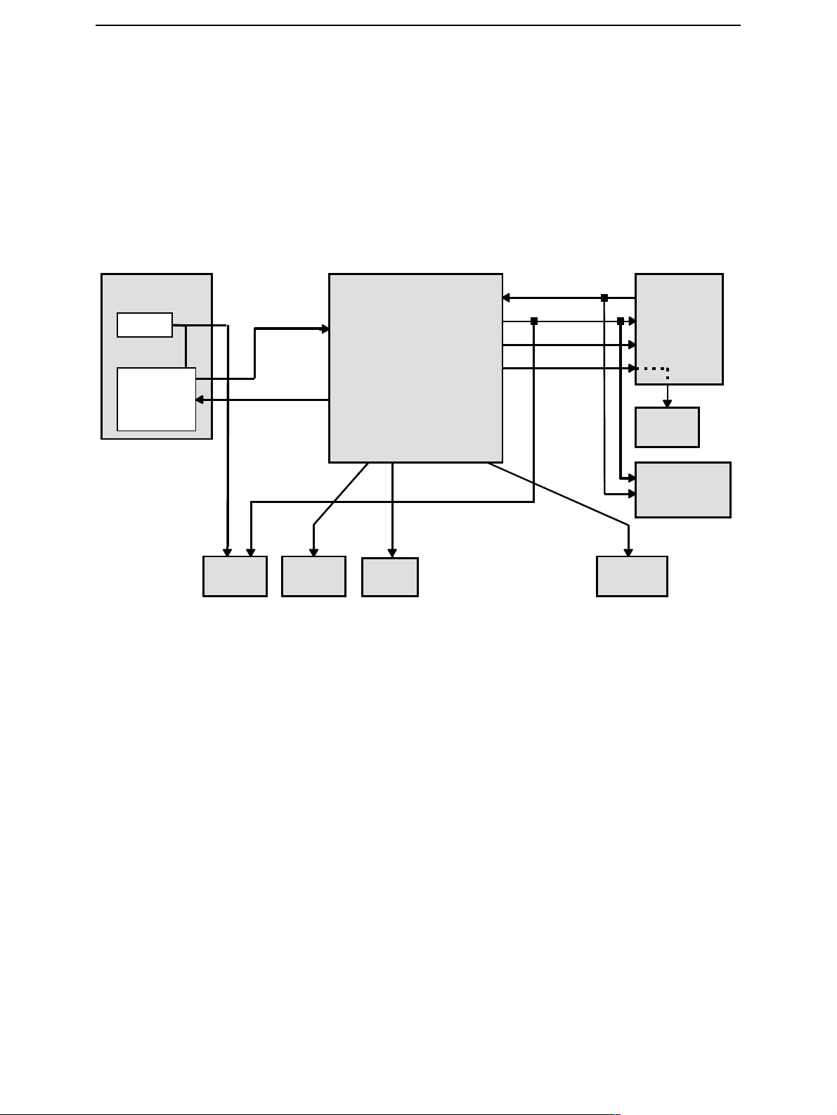
Clocks troubleshooting
C
S
S
C
S
D
The main clock signal for the baseband is generated from the voltage and temperature
controlled crystal oscillator VCTCXO (G591). This 26 MHz triangle wave clock signal is
supplied to OSC_IN pin of HAGAR. Inside HAGAR the clock frequency is divided to 13
MHz and then fed to RFCLK pin of UPP_WD2 and Bluetooth.
In SLEEP mode the VCTCXO is off. UEM generates low frequency clock signal (32.768
kHz) that is fed to UPP_WD2, Bluetooth and AEM.
CCS Technical Documentation
RF
VCXO
RF-ASIC
(Hagar)
LPRF
RFClk
13 MHz
RFBusCl
Flash
Clk
FLASHes
UPP_WD2 UEM
leepClk
BusCl
BusCl
IMCl
SIM
AEM
DRAM
lk
CAMERA
SDRAM
When the flashing of the device does not succeed, but powering is OK, follow these
instructions.
Note: The absence of clocks may indicate that the device (put phone to LOCAL mode
when the sleep is not allowed or press buttons so that phone is not in sleep mode) is in
sleep mode. Make sure that the device is not in sleep during RF clock measuring.
Ω
IMPORTANT: Clock signals have to be measured with 1M
(or greater) probes!
Page 16 ¤Nokia Corporation Issue 2 11/02
Page 19
CCS Technical Documentation
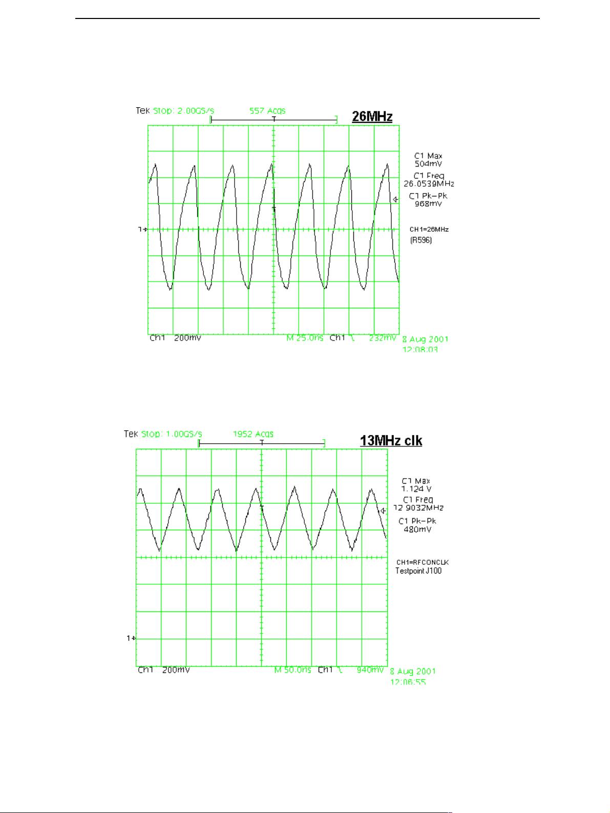
1 Measure signal from R596. This should be 26Mhz clock signal. See figure below.
If the clock not exist, check voltage from C662, it should be 2.78V (UEM regulator VR3). If voltage is OK, check G591 and other componets around it.
Figure 2: 26 Mhz clock
2 Check 13Mhz Rfclk from testpoint J100. See figure below. Offset should be
about 900mV. If the offset does not exist something is broken inside UPP_WD2
or DC-filtering capacitor in series on trace.
Figure 3: 13 MHz clock
Issue 2 11/02 ¤Nokia Corporation Page 17
Page 20
CCS Technical Documentation
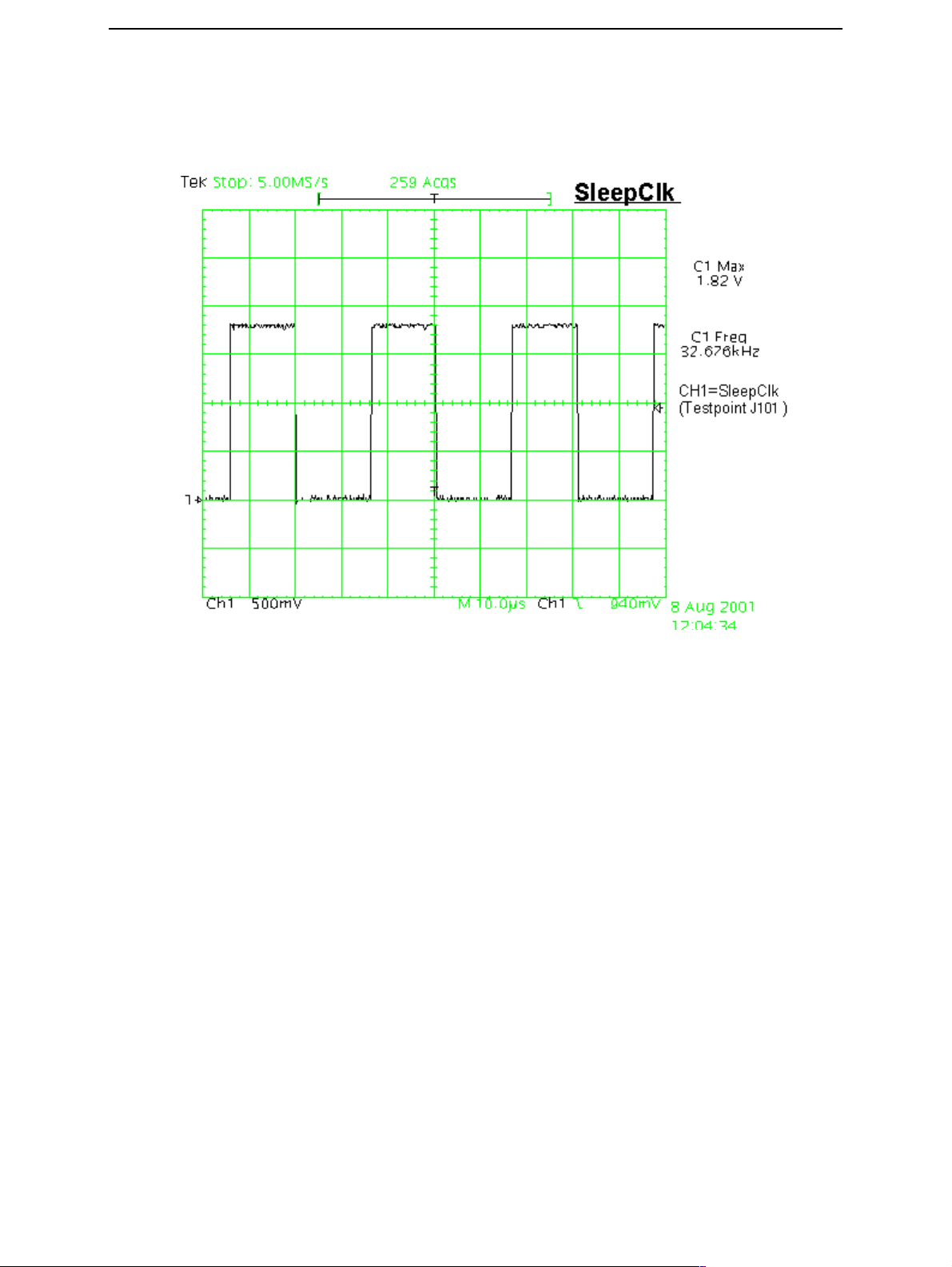
3 Check is the crystal oscillator (B190) oscillating at 32.768kHz frequency. If not
change B190. If OK measure sleepclk from testpoint J101. Frequency should be
the same 32.678kHz (see figure below.) If not change UEM.
Page 18 ¤Nokia Corporation Issue 2 11/02
Page 21

CCS Technical Documentation
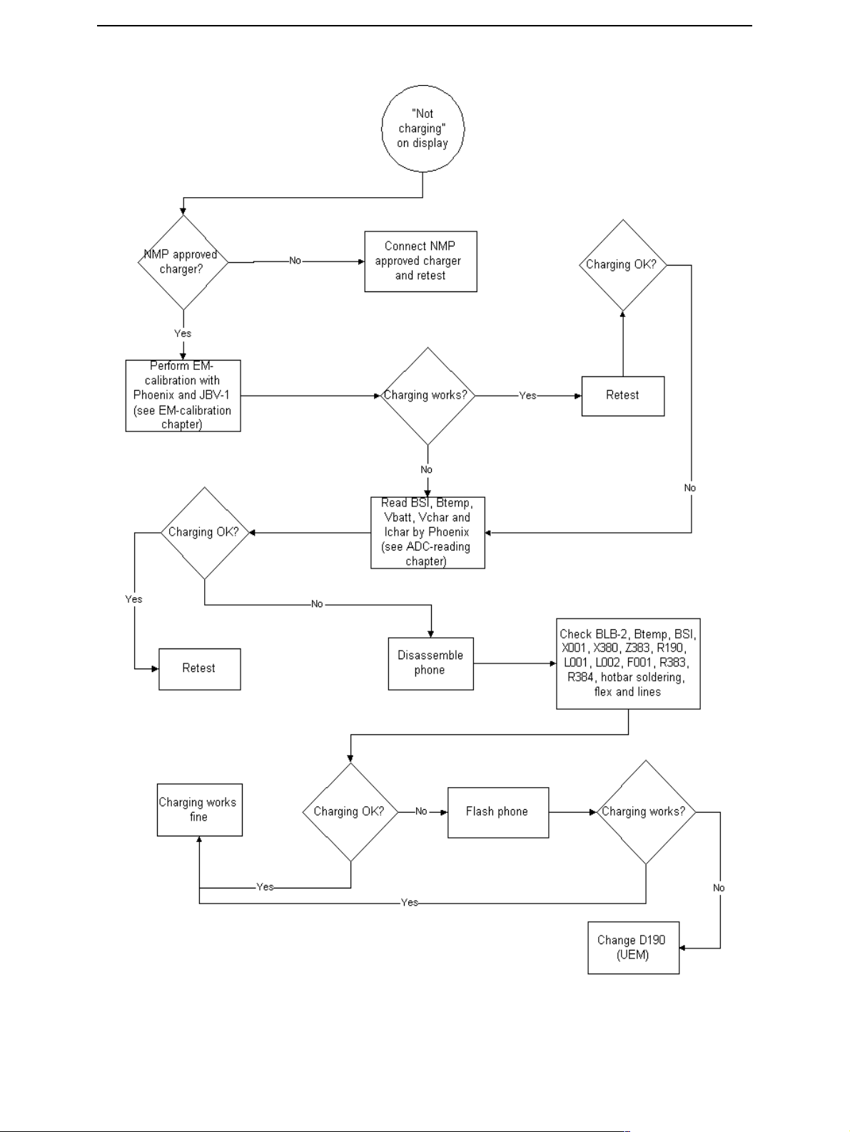
Charging checking
Use the BLB-2 battery and JBV-1 calibration set to test charging. (NOTE: power supply
cannot be charged if it not has a current sinking capability.) When you are charging
totally empty battery, remember that start-up charging might take a little bit longer time
than normal. During this time display is blank.
If charger is not NMP approved type and its current and voltage is not within NMP
charger window then software does not start charging and there is “NOT CHARGING” on
the display. Voltage should be between 5.5V - 9.3V and current between 200mA –
850mA
Remove and reconnect battery and charger few times before you start to measure
device. This check ensures that the fault really exists.
Issue 2 11/02 ¤Nokia Corporation Page 19
Page 22
CCS Technical Documentation
Page 20 ¤Nokia Corporation Issue 2 11/02
Page 23
CCS Technical Documentation
Issue 2 11/02 ¤Nokia Corporation Page 21
Page 24

Energy management calibration
During energy management calibration A/D-converter, BSI, Btemp, Battery voltage,
Charger voltage and Charger current are calibrated. For detailed information and
instructions see EM-calibration instructions in service manual.
Troubleshooting tips:
ADC-offset over limits:
Inspect BSI line, connectors (hotbar and board to board connector) and components in it
(Varistor R008, EMI-filter Z383, Pull-up resistor R384). If these are OK, change UEM.
BSI Gain over limits:
Inspect BSI line, connectors (hotbar and board to board connector) and components in it
(Varistor R008, Capacitor C002, EMI-filter Z383, Pull-up resistor R384). If these are OK,
change UEM.
Btemp Gain over limits:
Inspect Btemp line, connectors (hotbar and board to board connector) and components
in it (Varistor R006, Capacitor C010, EMI-filter Z383, Pull-up resistor R383). If these are
OK, change UEM.
CCS Technical Documentation
Vbatt offset and Gain:
Inspect Vbatt lines and component in it.
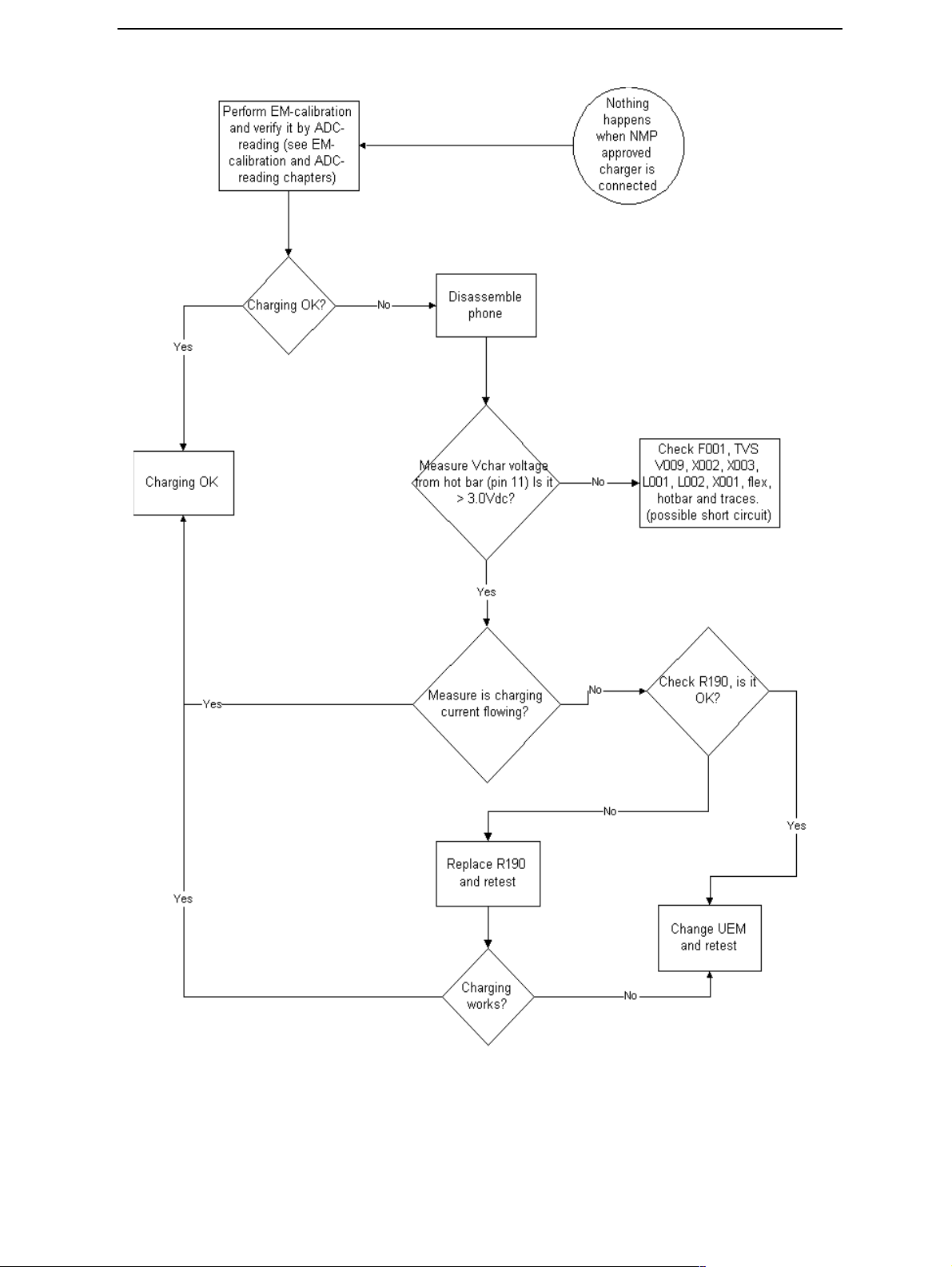
Vchar over limits:
Inspect components which are connected Vchar line: Filtering capacitors C005, C006,
C011, TVS V009, L001 and Fuse F001. If those are OK, Change UEM
Ichar over limits:
Inspect components which are connected at Vchar line: Filtering capacitors C005, C006,
C011, TVS V009, L001 and Fuse F001. If those are OK, First change current sense resistor
(R190), if calibration is not still successful change UEM.
Calibration can be checked using ADC-redings. Known voltages, currents and resistances
are fed and read by ADC-readings, read values and known values can be compared.
Page 22 ¤Nokia Corporation Issue 2 11/02
Page 25
CCS Technical Documentation
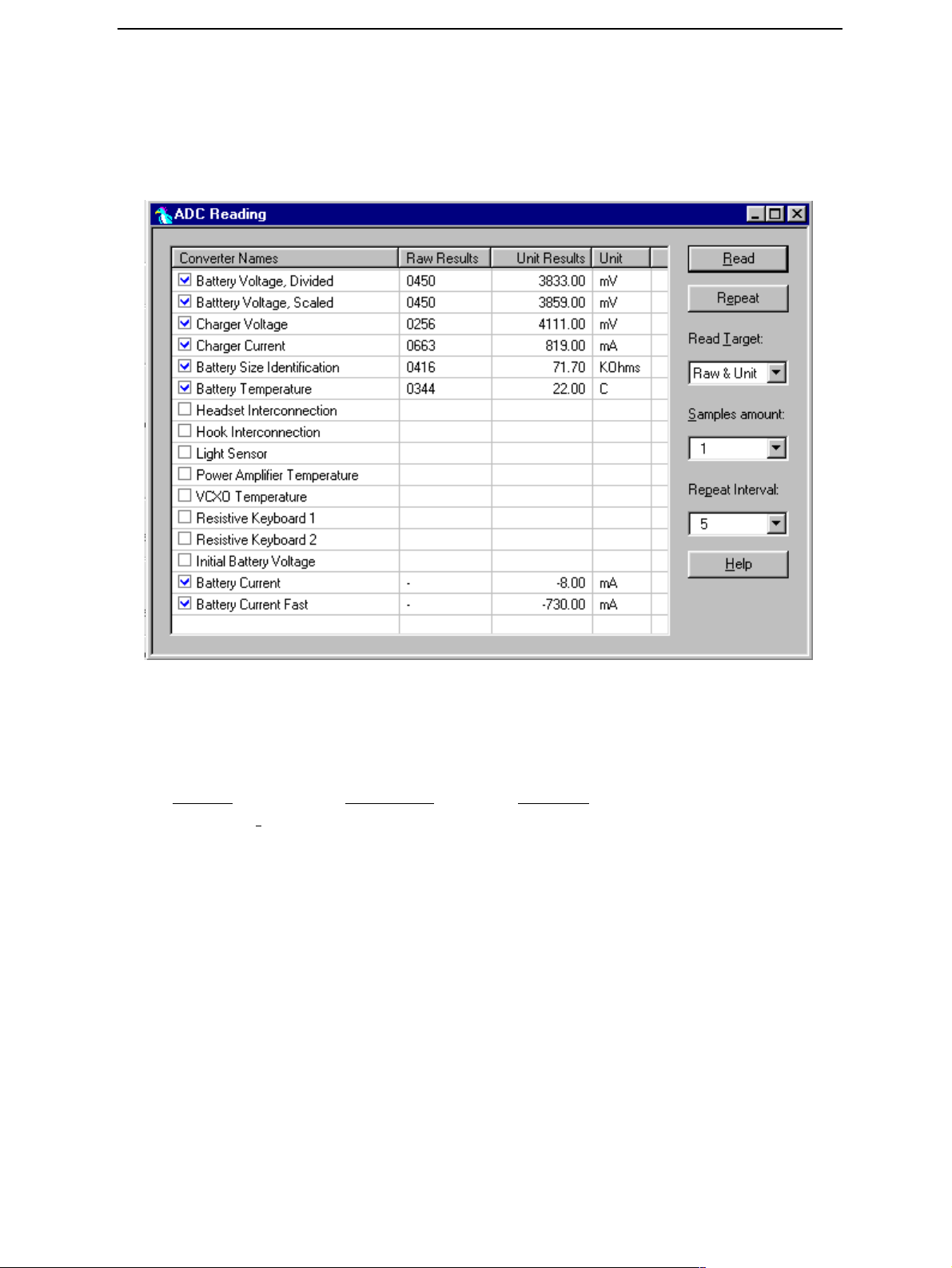
ADC-reading
Divided and scaled battery voltage, Charger voltage, Charger current, BSI and Btemp values can be read by this tool. Read values few times before you can be sure that results
are accurate.
Figure 4: ADC-readings view
Note:: If Vbatt Scaled and Divided unit results are different default calibration values
are used. In this case perform EM-calibration to get full performance of phone.
Maximum tolerances are:
Reading
Vbatt SCAL 4.2V ± 25mV
Vchar 8.4V ± 40mV
Ichar 500mA ± 20mA
BSI 68k(BLB-2) ± 1.3kohm
Btemp 273K(47k) ± 5K
Backup battery
Symptom of backup battery fault is:
Real Time Clock loses the correct time during short main battery removal.
The same syptom can also be seen when the backup battery is empty. About 5 hours is
needed to fully charge the backup battery in the device. NOTE: Backup battery is charged
only the same time with main battery charging. Or when the device is LOCAL or TEST
mode.
Check point Tolerance
Issue 2 11/02 ¤Nokia Corporation Page 23
Page 26
CCS Technical Documentation
Always check that the backup battery visually for any leakage or any other visual defect.
Check that the backup battery is correctly mounted in the device before closing the
cover.
1 Check with Phoenix is backup battery OK
2 Measure the voltage of backup battery
• Normal operation when the voltage is > 2.0V
• Fully charged when the voltage is about 3.2V (because of large internal imped
ance voltage won’t stay above 3.0V a long time after charging is disabled)
3 Enable backup battery charging (start to charge main battery or boot device to
LOCAL or TEST mode)
4 Measure voltage of backup battery during charging, It should arise if it is not
3.2V, yet.
5 When the voltage is over 2.0V for sure, check backup battery with Phoenix.
-> If not OK then D190 is faulty.
6 Ensure that the RTC is running.
IR interface
0. IR test
1. IR test
s
e
y
2. IR ok
Re-flash,ifnot
working its
beyond
economical
repair
no 3. IR selftest
4. Remove Acover (refer to
disassebly
instructions)
5. Repeat IR
no
6. Replace IR
module, repeat
s
e
y
test
noyes
test
2. IR ok
o
n
e
y
s
4. Remove Acover
Replace A-
cover
5. Repeat IR
test
yes
soldering of
GND (pins 5
soldering of
serial resistors
and capacitors,
o
n
8. Check
Vcc and
and 8)
yes
10. Check
the rest of
the pins.
s
e
y
7. Replace
repeat test
7. Replace
serial resistors
and capacitors,
repeat test
no
Beyond
economical
repair
no
no
no
yes
9. Check
capacitors
C360-363
o
n
Fix and repeat
test
6. Replace IR
module and
test again
no
If test fails after
re-flash, phone
is beyond
economical
repair
2. IR ok
yes
PWB fail
s
e
y
no
Page 24 ¤Nokia Corporation Issue 2 11/02
Page 27

CCS Technical Documentation
0. At this point it is supposed that problem is in HW
1. Send something to another phone or laptop
2. Everything is ok
3. Activate phones IrDA selftest
4. Take off phones A-cover
5. Start test again from the beginning, there might be more than one fault...
6. Solder a new IrDA module to phone, start test again.
7. Replace resistors R360 – R363 and capacitors C360-C363
8. Vcc in pin 5 should be connected to VMEMA
9. Check capacitors C360-363 for shorts and open contacts
10. Pin 1 (Anode) should be at battery voltage, pin 2 (Cathode) should be floating, pin 3
(Tx), pin 4 (Rx), pin 7 (mode) should be grounded.
Issue 2 11/02 ¤Nokia Corporation Page 25
Page 28

Sensors troubleshooting
This part of document is written to help troubleshooting for proximity sensor and ambient light sensor in NHL-2NA. Both of them are calibrated in production, in FINUI tester.
AMS has possibility to calibrate proximity sensor at service points, ambient light sensor
is repaired in Bochum.
This document is ment to be used only in troubleshooting and does not provide information on basic functionality of the systems. Basic operating principle can be found in
chapter “System Module LG4 and Grip Module LS4”, calibration instructions can be
found in chapter “Service Software Instructions”.
CCS Technical Documentation
Page 26 ¤Nokia Corporation Issue 2 11/02
Page 29

CCS Technical Documentation
Proximity Detector
General notes
In the production proximity detector problems are best located from calibration results.
Before starting troubleshooting with the help of this section, user should familiarize to
the calibration instructions.
When the user brings the phone to the service point complaining that handsfree won’t
turn on, the problem can be either in the handsfree speaker circuitry, or in the proximity
detector. This chapter gives instructions how to repair the problem in the proximity
detector.
A good indicator that the proximity detector has caused disabling of the loudspeaker is,
that the phone has switched the audio back to the earpiece. If the audio is not switched
to the earpiece but also loudspeaker is not on, the problem is most likely in the handsfree
circuitry.
When the problem is located on the proximity detector, always replace lens module
before proceeding to detailed troubleshooting.
If the problem is not this simple, the best way to look for the problem is to use PD calibration results.
Remember that Proximity Detector has to be calibrated always when optocomponents or
optics are replaced! Calibration also has to be done, if AEM ASIC is replaced or if calibration settings are lost from PMM.
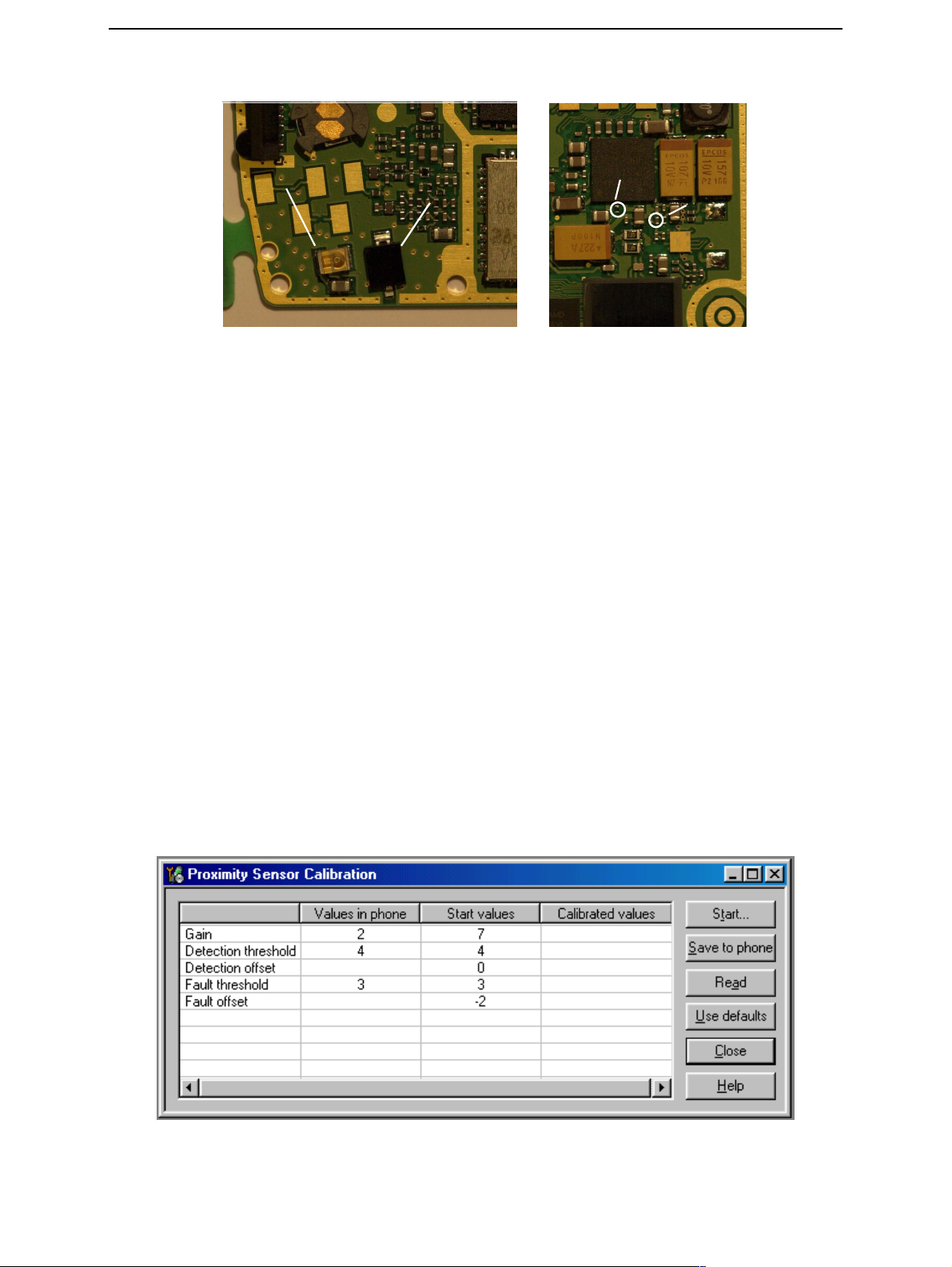
Proximity Detector components
From now on Proximity Detector will be referred to as PD.
Main components of PD are lenses, emitter (IRED CL-200-IR, V334, 4860009), RSENSE
4R3 (R347), receiver (photodiode BPW34FS, V335, 4864911) and a control block, which is
located on AEM ASIC (N226). Three external capacitors are part of the control block:
100n (C275) and 220p (C273 and C274).
Issue 2 11/02 ¤Nokia Corporation Page 27
Page 30
CCS Technical Documentation
Figure 5: Most important receiver and transmitter components
V334 V335
Handsfree shuts down automaticallly in sunshine
It is normal, if this behaviour occurs only in high ambient light conditions, e.g. direct
sunlight, and no repair actions are needed. If this problem occurs also in low ambient
light conditions (outdoors when the phone is not facing the sun), check that capacitors
C273, C274 and C275 are placed correctly. Replace the lens module and recalibrate the
system.
PD calibration
Proximity Sensor Calibration tool is shown in the Figure 4 Proximity Sensor Calibration
tool. Parameters that are calibrated and saved to PMM are gain, detection threshold and
fault detection threshold. When you start the calibration tool, the values in the PMM are
shown in the left column. Second column shows start values used in calibration, they
are defined by R&D. Calibration consists of two phases. First gain and detection threshold are calibrated. If this calibration is finished successfully, software starts fault threshold calibration; fault threshold cannot be calibrated alone. Offset value(s) are used to
adjust the thresholds to compensate possible wearing of the PD. To help troubleshooting
phone SW response is one of the 13 messages that are explained in the next chapter.
Successful gain and detect threshold calibration tells that optoelectrical components are
OK. Note! Values in this picture might change.
R347
C275
Figure 6: Proximity Sensor Calibration tool
Page 28 ¤Nokia Corporation Issue 2 11/02
Page 31

CCS Technical Documentation
Troubleshooting with PD Calibration results
CALIB OK (0x00)
This is the response, when calibration is done successfully. Save calibration results to the
phone.
START ILLEGAL PARAMETER (0x01)
Calibration starts with rough check for start values. Detection threshold, gain and fault
detection threshold must be between 0 and 7; offset for both of them is from -7 to 7.
Default start parameters never fail to meet these limits. Check that correct limits are
used in the calibration SW (PC or Phoenix) and try calibration again.
PXM GAIN INT FAIL (0x02)
This should be impossible. If, however, you manage to get this error, try calibration again.
DET TR FAIL (0x03)
An error has occurred during calibration. Try calibration again. If no result is obtained in
three calibrations, replace proximity optics.
Another option is, that detection offset is too big for calibrated detection threshold. This
isn’t possible, if start values are correct. Use default start values.
OFFSET FAIL (0x05)
Selected offset could not be used with this calibration result. Check, that you have used
correct default offset. Then replace the optics.
DET NOT DONE (0x06)
Fault calibration can be done only directly after detect calibration. If, for example, the
phone was restarted between fault –and detect calibration, this error occurs. Repeat
whole calibration.
COMBINATION FAIL (0x07) / W OFF FAIL (0x08)
Calibrated detection threshold, fault detection threshold and detection offset form a
combination that is not allowed. Use default start values in calibration and check that
proximity rubber is OK. If this does not help, replace optics.
FAULT INT FAIL (0x09)
This error occurs, if self-monitoring signal is too small to exceed any fault threshold
(when offset is added). This error occurs also if there is a detection during fault threshold
calibration.
Issue 2 11/02 ¤Nokia Corporation Page 29
Page 32

CCS Technical Documentation
Is proximity optics and proximity rubber OK (visual check)? If not, replace optics. Check
calibration conditions and repeat calibration.
FAULT OVER LIMIT FAIL (0x10)
This error occurs in fault detection threshold calibration, if self-monitoring signal is
higher than each fault detection threshold. There are two reasons, that could cause this
failure:
Detection calibration is done without the calibration target or the target was too far
from the phone.
Fault calibration was done with the calibration target.
Check calibration conditions and repeat calibration.
GAIN MAX LIMIT FAIL (0x0B)
Gain value has reached its maximum limit, and there are no detections. This means, that
path from tx to rx is broken. Most probable is, that the failure is on the LG4. Figure 5
GAIN MAX LIMIT FAIL troubleshooting presents troubleshooting diagram for this failure.
Page 30 ¤Nokia Corporation Issue 2 11/02
Page 33

CCS Technical Documentation
S
G
Figure 7: GAIN MAX LIMIT FAIL troubleshooting
GAIN MAX
LIMIT FAIL
Was
reflectance
target
properly
placed?
YES
Disassemble the
phone to MJS-9Q
Check TX and RX
path, replace needed
components, fix solder
problems (1)
Try calibration in the
MJS-9Q
GAIN MAX
LIMIT
FAIL?
NO
NO
YES
Fix thetarget and
repeat calibration
Replace AEM
calibration
ave calibrated values
to the phone
Try calibration in the
MJS-9Q
Is
OK?
YES
NO
Follow respective
error message
AIN MAX
LIMIT
FAIL?
NO
YES
Beyond economical
repair
Reassemble the phone,
replace optics.
Is
calibration
OK?
YES
Save calibrated values
to the phone
1 PD TX line: RSENSE R347 is connected to GND and IRED V334 to Vbatt
RX line: photodiode V335 is connected to GND. See figure 5.
2 If there is no obvious fault, replace first V335, then V334. Try calibration in the
MJS-9Q in between.
Follow respective error
message
Issue 2 11/02 ¤Nokia Corporation Page 31
Page 34

CCS Technical Documentation
S
S
GAIN MIN LIMIT FAIL (0x0C)
There is a detection at each gain. IRED, RSENSE and photodiode are OK. Possible reasons
are shortcut in RSENSE, missing optical insulator or wrong start values in calibration.
Figure 8: GAIN MIN LIMIT FAIL troubleshooting
GAIN MIN
LIMIT FAIL
Is the
calibration
done
correctly?
YES
Disasseble the phone
to MJS-9Q
Proximity
rubber OK?
Screws
were tight?
YES
Is RSENSE
4R3 and
soldering
OK?
YES
NO Check correct start
values from Sensor
Calibration Instructions
and repeat calibration.
NO
NO
Replace
RSENSE
Is
calibration
OK?
YES
ave calibrated values
to the phone
NO
Follow respective
error message
Replace AEM
Try calibration in MJS9Q
GAIN MIN
LIMITFAIL?
YES
If you have checked
mechanics, RSENSE
and AEM the phone
is beond economical
repair
NO
Reassemble the phone,
replace proximity rubber
and optcs if needed
Is
calibration
OK?
YES
avecalibratedvalues
to the phone
NO
Follow respective
error message
Page 32 ¤Nokia Corporation Issue 2 11/02
Page 35

CCS Technical Documentation
Ambient Light Detector
General Notes
Ambient light sensor problems can be found during the calibration process or as problems with the display backlight and grip LEDs. The problem can also be in the NTC-resistor, which is used for temperature compensation of the ambient light detector. Before
starting troubleshooting according to these instructions, it must be ensured that the
problem really is in the ambient light detector. Other possibility is e.g. UI-module or
backlight powering itself. This can be checked easily, because light sensor can be turned
off.
Calibration of the Ambient Light Detector is needed always, when the phototransistor is
replaced.
Calibration system is described in chapter “Service Software Instructions”.
Figure 9: Ambient light detector calibration tool
Issue 2 11/02 ¤Nokia Corporation Page 33
Page 36

Ambient Light Detector
R
R
From now on the Ambient Light Detector will be referred to as ALD.
Main components of the ALD are phototransistor SFH3410 (V130, 4864901), pull-up
resistor 22kΩ (R131) and UEM (D190) ADC. There is also an NTC-resistor 47kΩ (R132,
1820037), which is used for temperature compensation. Temperature compensation is
done by SW.
CCS Technical Documentation
Figure 10: Ambient Light Sensor components
V130
(collector)
132
V130
(emitter)
131
Page 34 ¤Nokia Corporation Issue 2 11/02
Page 37

CCS Technical Documentation
r
p
Problems from the user point of view
“The sensor doesn’t control backlights of the phone”
Figure 11: ALD troubleshooting 1
“The light sensor never
controls backlights of
the phone.” “Backlight
alwayson.”
Is light
sensor set
on?
Yes
Are
backlights
off in bright
light? (1)
Yes
ALD circuitry is working
No
No
Set the sensor to
“Maximum”.
Use Phoenix to see
ADC-readings and
VCXOTEMP. Read the
sensor in bright light.
Does sensor
reading
change with
illumination?
(2)
Is
VCXOtemp
readind
around the
ight value?
Are ADCreadings
OK?
Yes
Yes
No
No
No
Disassemble the
phone to MJS-9Q
Disassemble the
phone to MJS-9Q
Replace UEM
Check pull-up resistor
and phototransistor (3)
Check pull-up resistor
and NTC resistor (4)
If this does not help, the
problem is beond economical
repair.
Yes
Reassemblethe
hone
Is ALD
mechanics
OK?
(5)
No
Replace A-cover
Yes
Calibratethe light
sensor
Issue 2 11/02 ¤Nokia Corporation Page 35
Page 38

CCS Technical Documentation
1 Set light sensor sensitivity to minimum. Illuminate sensor from close range with
very bright light.
2 Sensor ADC-reading should be <500 in bright light and in total darkness >900.
3 Check that resistance between sensor collector and VFLASH1 is 22kΩ (R131).
Check that resistance between collector and emitter of the ambient light sensor
changes, when illumination on the sensor (from ~5kΩ in high illuminance to
~500kΩ in total darkness) (V130). If phototransistor has to be replaced, the
detector has to be calibrated. Calibration can be done only with TDS-11 light
source.
4 NTC ( R132) resistance at room temperature is ~47kΩ.
5 Check following points: is opening on the black paint in the A-cover covered; is
light guide (integrated in the A-cover) broken?
Page 36 ¤Nokia Corporation Issue 2 11/02
Page 39

CCS Technical Documentation
V
r
“Backlights are never ON”
Figure 12: ALD troubleshooting 2
“Ba cklight is
never ON.”
IsBa c k lig h t
ON, when
Light Sensor
settingis
OFF?
Yes
Are
backlights
ON in
darkness?
Yes
AL Dcircu itryiswork in g
Ca libratethelight
sensor.
No
Go to Backlight
Troubleshooting
No No
UsePhoenix to see
ADC-readings and
VCXOTEMP
Does sensor
reading
change with
illum ination?
(2)
Yes
Is
CXOtemp
readind
around the
ight value?
No
Yes
Disasseblethe
phonetoMJS-9Q
Disassemblethe
phone to MJS-9Q
Check VFLASH1, pull-up
resistor and ambient light
)
sensor (3
Check pull-up resistor
andNTCresistor (4)
Calibratethelight
sensor.
Isthe
fun ctionality
OK?
No
Problem isbeyond
economical repair
Yes
Select default setting
for thelight sensor.
Issue 2 11/02 ¤Nokia Corporation Page 37
Page 40

CCS Technical Documentation
1 Set light sensor sensitivity to “minimum”. Cover ALD window for example with a
hand.
2 Sensor ADC-reading should be <500 in bright light and in total darkness >900.
3 Vflash1, measured at pull-up resistor pin, should be 2.78V. Check that resistor
R131 is placed, and it’s resistance is 22kΩ. Check that resistance between collector and emitter of the ambient light sensor changes, when illumination on the
sensor (from ~5kΩ in high illuminance to ~500kΩ in total darkness). If phototransistor has to be replaced, the detector has to be calibrated. Calibration can
be done only with TDS-11 light source.
4 NTC ( R132) resistance at room temperature is ~47kΩ.
Page 38 ¤Nokia Corporation Issue 2 11/02
Page 41

CCS Technical Documentation
SIM card
The whole SIM interface locates in two chips UPP_WD2 and UEM. UEM contains the SIM
interface logic level shifting. UPP provides SIMClk through UEM to the SIM. SIM interface supports both 3 V and 1.8 V SIMs. There is an EMI component on lg4 between the
sim card and UEM which isn't shown in the below picture. One pullup resistor is also on
board at simdata line, which isn't shown in the picture.
Figure 13: UPP WD2 & UEM SIM connections
GND
UPP
SIM
C5 C6 C7
C1C2C3
BSI line from battery
SIMCLK
SIMRST
BSI
SIMDATA
VSIM
GND
UEM
SIMIF
register
SIMIO
SIMClk
Data
UEM
digital
logic
SIMIO
SIMClk
Data
UIF Block
UEMInt
CBusDa
CBusEnX
CBusClk
The SIM-power up/down sequence is generated in the UEM. This means that the UEM
generates the RST signal to the SIM. Also the SIMCardDet signal is connected to UEM.
First the SW attempts to power up the SIM with 1.8 V. If this does not succeed power up
is repeated with VSIM switched to 3 V.
The data communication between the card and the phone is asynchronous half duplex.
The clock supplied to the card is in GSM system 1.083 MHz or 3.25 MHz. The data
baudrate is SIM card clock frequency divided by 372 (by default), 64, 32 or 16.
Issue 2 11/02 ¤Nokia Corporation Page 39
Page 42

Figure 14: SIM Power Up.
CCS Technical Documentation
Ch1 Vsim
Ch2 Reset
Ch3 Clock
Ch4 I/O
Measured with
3Vsim
Figure 15:
SIM answer to reset
-Ch1 Vsim
-Ch2 sim_data
–Ch3 sim_clk
–Ch4 sim_reset
Page 40 ¤Nokia Corporation Issue 2 11/02
Page 43

CCS Technical Documentation
Figure 16: SIM Clk 3.25MHz
Issue 2 11/02 ¤Nokia Corporation Page 41
Page 44

CCS Technical Documentation
"Insert SIM Card" in device display allthough card is inserted
Sim card
faults
Check sim BB
self tests. Are
they ok?
Yes
Check SIM
connector
Is it ok?
Yes
Measure VSIM
voltage from jig
is it 1.8/3.0V at
powerup?
No
No
No
Either UPP_WD2 or UEM is
faulty. Change UEM first
and if still fails the tests
change UPP_WD2
Clean pwb pads and
connector / change
connector
Check Vsim resistance to
gnd (no power) if low ->
measure C470 -> if ok
change R470 -> still not
ok -> change UEM
Yes
No
Check SIM
power up
sequence
Is it ok?
Check Vsim resistance to
gnd (no power) if low ->
measure C470 -> if ok
change R470 -> still not
ok -> change UEM
Page 42 ¤Nokia Corporation Issue 2 11/02
Page 45

CCS Technical Documentation
Audio
Microphone
Issue 2 11/02 ¤Nokia Corporation Page 43
Page 46

Earpiece
CCS Technical Documentation
Check that holes are not covered.
Page 44 ¤Nokia Corporation Issue 2 11/02
Page 47

CCS Technical Documentation
IHF
In the case of IHF fault the reason can be found from integrated hands free itself or
proximity sensor. Proximity sensor disables IHF if phone is too near some object. It is possible if the proximity sensor is faulty IHF can not be enabled even if it is working fine.
Issue 2 11/02 ¤Nokia Corporation Page 45
Page 48

Accessory detection troubleshooting
CCS Technical Documentation
Page 46 ¤Nokia Corporation Issue 2 11/02
Page 49

CCS Technical Documentation
Memory troubleshooting
Most memory related errors are found through flashing the device, flashing the device is
therefore recommended before any of the steps described in this chapter. Check flashing
troubleshooting section first.
There are however a few memory related errors that cannot be found through flashing.
• SDRAM partially damaged
This can mean that the sdram component itself is partially damaged and all the
memory locations cannot be successfully accessed or there is a soldering problem
somewhere either under UPP or sdram.
Sdram fault
suspected
Yes
Run sdram BB selftest
If fail -> change sdram ->
retest -> if still fails ->
change UPP WD2
Change
sdram
No
Does the phone
boot to local
mode?
• flash1 (D310) is partially/totally damaged
During flashing the manufacturer, device and revision id's are read, but flashing
is done based on id's of the flash0 (D311). This means that one cannot see any
error messages displayed on Phoenix window during flashing if flash1 is failing.
Id's are however displayed on the Phoenix window and successful read of flash1
id's can be checked from there. One good way to test flash1 functionality is to
format it(from Phoenix).
Issue 2 11/02 ¤Nokia Corporation Page 47
Page 50

Baseband serial interface troubleshooting
CBUS
CBUS is a three wire serial interface between main baseband components. The bus consists of data, clock and bus_enable signals. In NHL-2NA the bus is connected from UPP
WD2 to AEM, UEM and the BT module. UPP_WD2 takes care of controlling the traffic on
the bus.
If the interface is faulty from the UPP WD2's end the phone will not boot properly as
powering configurations do not work. Traffic on the bus can be monitored from three
pins on the BT module. Pins are shown below.
Figure 17: CBUS measuring points
CCS Technical Documentation
CBusClk
CBusDa
CBusEnx
Page 48 ¤Nokia Corporation Issue 2 11/02
Page 51

CCS Technical Documentation
In the pictures below CBUS traffic at bootup is shown. CbusEnx is connected to Ch1,
Cbus Da to Ch2 and CbusClk to Ch3. The lower is just a more detailed picture of a write
command (to AEM).
However, if you are able to get the phone to boot up and can reach Phoenix BB self tests
it is possible to test the functionality of each component attached to Cbus. Use:
• ST_AEM_CBUS_IF_TEST to test AEM Cbus interface
• ST_UEM_CBUS_IF_TEST to test UEM Cbus interface
• ST_LPRF_IF_TEST to test Bluetooth Cbus interface
If an error is found testing any of the abowe components you should replace or re-solder
the failing component.
Issue 2 11/02 ¤Nokia Corporation Page 49
Page 52

FBUS
MBUS
CCS Technical Documentation
FBUS is a two wire RX and TX interface between UPP and flash/test interface. The bus
goes through UEM which adjusts the voltage levels to suit UPP_WD2. The interface voltage level on the phone flash/test pad pattern is 2.78V and on the UPP WD2 end it is 1.8V.
The functionality of this interface should not affect the device boot into NORMAL, LOCAL
nor TEST modes. Phoenix tests can be performed through MBUS interface in the case of a
failure in FBUS interface. Flashing is not possible if there is a problem in FBUS interface.
MBUS is a two wire RX and TX interface between UPP and UEM. From UEM the interface
continues to flash/test interface as a one wire interface. UEM adjusts the voltage levels.
The interface voltage level on the phone flash/test pad pattern is 2.78V and on the UPP
WD2 end it is 1.8V. MBUS traffic between UPP WD2 and UEM can be tested with PHOENIX (ST_MBUS_RX_TX_LOOP_TEST). Flashing is not possible if there is a problem in
MBUS.
Page 50 ¤Nokia Corporation Issue 2 11/02
Page 53

CCS Technical Documentation
Hall sensor troubleshooting
There might be two kind of malfunction concerning Hall sensor; The out put of the Hall
sensor keeps to high or low regardless the position of the magnet.
Hall sensor
malfunction
Phone thinks grip is
open all the time
Check that magnet is
in its place and it's as
effective as specified
Measure that N380 is
properly soldered and it
has ~2.78V in pin 1. Pin
3 should be down when
magnet is not above the
component. ~1.8V
when magnet is above
it.
no
Phone thinks grip is
closed all the time
yes
Change the N380 to a
new one and retest.
Hall sensor works
Issue 2 11/02 ¤Nokia Corporation Page 51
Page 54

Display backlights troubleshooting
CCS Technical Documentation
Page 52 ¤Nokia Corporation Issue 2 11/02
Page 55

CCS Technical Documentation
Bluetooth troubleshooting
BT Failure
Part I
(Flashing problems)
Attempt to re-flash
the phone
Do you have
any FPS-8
errors?
Yes
No
Does the
phone's main
SW flash
correctly?
Yes
Does the BT
SW flash
correctly?
Yes
BT Flashing OK!
No
No
Go to Calypso's
'Flashing'
Troubleshooting
Section
1) Replace
BT MCM
2) Attempt to
Flash Phone
Issue 2 11/02 ¤Nokia Corporation Page 53
Page 56

BT Failure
Part II
(BER Failure)
Test Pogo-Pin
connection to BT
antenna
with multimeter
Are the Pogo-
Pins electrically
connected to
BT antenna
(i.e. short
circuit)?
Yes
Visually check BT
antenna
CCS Technical Documentation
Replace
No
BT antenna
(i.e.new chassis)
Go to
BT Failure
Part III
No
Is BT antenna
attached
properly to
chassis?
Yes
Check soldering of
BT MCM with
microscope
Is BT MCM
propely
soldered to the
PWB?
No
Is BER < =
0.1%?
Yes
BT OK!
Yes
Yes
Is soldering so
bad that you
No Yes
must remove
BT MCM?
No
Re-solder
BT MCM
Production Only
Replace BT MCM
Re-Flash phone
using option
BT ONLY
Can you make
a connection to
BT Box?
No
Go to
BT Failure
Part III
Page 54 ¤Nokia Corporation Issue 2 11/02
Page 57

CCS Technical Documentation
BT Failure
Part III
(BER Failure)
Check VCC
(Pins 52, 53, 54)
with O-scope
Does VCC =
2.95 - 5.2
VDC?
No
Yes
Does Ripple
Voltage
< = 400mVpp?
Yes
Check VREG
(Pin 6)
with O-scope
Does VREG =
2.7-3.3VDC?
Yes
Does Ripple
Voltage
< = 30mVpp?
No
No
Check
VBAT / L430 /
C431
No
Check
VFLASH1 / L431
Check SYSCLCK
(Pin 50 )
with O-scope
Does Vin =
300-900mVpp?
Yes
Does Freq. =
26MHz?
No
Check
VCTCXO
No
Buffer Section
Yes
Yes
1) Replace
Can you make
a connection to
BT Box?
No
1) Replace
BT MCM
2) Flash Phone
using 'BT ONLY'
Yes No
Is BER < =
0.1%?
Yes
BT OK!
BT MCM
2) Flash Phone
using 'BT ONLY'
Issue 2 11/02 ¤Nokia Corporation Page 55
Page 58

Needed actions if ASIC is changed
UEM changed
If UEM is changed baseband calibrations should be made. IMEI has to be rebuilt to the
phone.
AEM changed
If AEM is changed proximity and ambient light sensor calibrations should be achieved.
UPP_WD2 changed
Device has to be reflashed.
Flash0 changed
IMEI has to be reprogrammed. Has to be flashed (naturally). IMEI has to be rebuilt to the
phone.
CCS Technical Documentation
RF component changed
If any RF component changed, RF calibration(tuning) has to be done.
Page 56 ¤Nokia Corporation Issue 2 11/02
Page 59

CCS Technical Documentation
Test points and pin orders
Test points in BaseBand area (LG4_06_02)
J100 RFclk
J101 Sleepclk
J102 SleepX
J103 PURX
J116 Txid
J117 Txqd
J118 Auxda
J119 Rxid
J120 Rxqd
J104 UEMint
J105 AEMSleep
J110 DSPVcc
J106 SDRda0
J107 SDRad0
J108 SDRclk
J109 FLDa0
J 111 F LXS 1x
J113 FLCS0x
J114 FLOEX
J115 FLClk
J121 I_FBUS_TX
J381 Vbatt
J270 GenVbattIO
J262 Refen
Issue 2 11/02 ¤Nokia Corporation Page 57
Page 60

CCS Technical Documentation
Page 58 ¤Nokia Corporation Issue 2 11/02
Page 61

CCS Technical Documentation
Connectors pin order
UI-connector
Pin
no.
1 VDD IN 2.78 V Voltage supply
2 GND 0 V System ground
3 D4 IN
4 D0 IN
5 A0 IN V H: data
6 GND 0 V System ground
7 VDDI IN 1.8 V Logic voltage supply
8 D1 IN
9 D2 IN
Signal name Type Typical Unit Description
V Data to write
OUT
OUT
OUT
OUT
V Data to read
V Data to write
V Data to read
L: command
V Data to write
V Data to read
V Data to write
V Data to read
10 D3 IN
OUT
11 Rocker3 200 mOhm
12 Rocker2 200 mOhm
13 GND 0 V System ground
14 Rocker5 200 mOhm
15 Rocker4 200 mOhm
16 Rocker1 200 mOhm
17 V
18 V
19 Row1 IN/
20 Row0 IN/
+ IN/
LED
- IN/
LED
4.5 V LED, positive terminal
OUT
0 V LED, negative terminal
OUT
OUT
OUT
V Data to write
V Data to read
Ohm Tracking resistance
mA Drive current
Ohm Tracking resistance
mA Drive current
mA Drive current
Issue 2 11/02 ¤Nokia Corporation Page 59
Page 62

CCS Technical Documentation
21 Col1 IN/
OUT
22 Col0 IN/
OUT
23 GND 0 V System ground
24 RESX IN V Reset
25 D5 IN
OUT
26 D6 IN
OUT
27 D7 IN
OUT
28 GND 0 System ground
29 RDX IN L: read
Ohm Tracking resistance
mA Drive current
Ohm Tracking resistance
mA Drive current
(active low)
V Data to write
V Data to read
V Data to write
V Data to read
V Data to write
V Data to read
(active low)
30 WRX IN L: Write
(active low)
Page 60 ¤Nokia Corporation Issue 2 11/02
Page 63

CCS Technical Documentation
Board to board connector
See System Module LG4 and Grip Module LS4”.
Pin order of spring connectors
Issue 2 11/02 ¤Nokia Corporation Page 61
Page 64

CCS Technical Documentation
Page 62 ¤Nokia Corporation Issue 2 11/02
Page 65

CCS Technical Documentation
RF Troubleshooting
Introduction
Measurements should be done using Spectrum Analyzer with high-frequency 1kW (20:1)
passive probe (LO-/reference frequencies and RF-power levels) and Oscilloscope with a
10:1 probe (DC-voltages and low frequency signals).
Please note that the grounding of the PA-module is directly below PA-module so it is difficult to check or change. Most RF semiconductors are static discharge sensitive! So
ESD protection must be taken during repair (ground straps and ESD soldering irons). The
Hagar IC is moisture sensitive so parts must be pre-baked prior to soldering.
Apart from key-components described in this document here are a lot of discrete components (resistors, inductors and capacitors) which troubleshooting is done by checking if
soldering of the component is done properly, for factory repairs (checking if it is missing
from PCB). Capacitors can be checked for shortening and resistors for value by means of
an ohmmeter, but be aware in-circuit measurements should be evaluated carefully.
Please be aware that all measured voltages or RF levels in this document are rough
figures. Especially RF levels varies due to different measuring equipment or different
grounding of the used probe.
All tuning must be done with Phoenix Service Software, version 02.90.001, or later.
Issue 2 11/02 ¤Nokia Corporation Page 63
Page 66

RF Key component placement
CCS Technical Documentation
Page 64 ¤Nokia Corporation Issue 2 11/02
Page 67

CCS Technical Documentation
9
T
TXQTXIR
R
R
Fault finding test point locations
900 LNAB_G
900 ASM RX
900 LNAi/p
1800 ASM RX
1800 LNAi/p
900 PAo/p
1800 PAo/p
900 LNAo/p
900 PABIAS
900 LNA_G
900 SAWi/p
1800 SAWi/p
1800 SAWo/p
1800 LNA_P
1800 PACONTROL
900 TXBALUN i /p
1800 LNAB_P
1800 PABIAS
00 SAWo/p
1800 TXFILTi/p
VR6
VCO BALUN o/p
900 PACONTROL
VR2
1800 PAi/p
900 PAi/p
XC
RX_I
VrefRF02
eset
VCO VCC
4G VCO o/p
VCO CONT ROL
VrefRF01
FBusClk
FBusEna1
VCT CXO o/p
RFBusDa ta
Issue 2 11/02 ¤Nokia Corporation Page 65
Page 68

Receiver
General description
CCS Technical Documentation
The receiver is a direct-conversion, dual-band linear receiver. RF signal energy gathered
by the antenna is fed via the antenna switch module to the 1
st
RX bandpass SAW filters
and MMIC LNAs. The RF antenna switch module provides for upper- and lower-band
operation. The signal having been amplified by the LNA is then fed to 2nd RX bandpass
SAW filters. Both of these 2nd RX bandpass SAW filters have UNBAL/BAL configuration to
achieve the balanced feed for HAGAR. The discrete LNAs have three gain levels. The first
one is maximum gain, the second one is about -30dB ( GSM1800 ) and –25dB ( EGSM900 ) below maximum gain and the last one is off state. The LNA gain selection is
controlled directly by HAGAR.
The performance of the RX bandpass SAW filters are mainly responsible for defining the
receiver's blocking characteristics against spurious signals outside passband and the protection against spurious responses.
The differential RX signal is amplified and mixed directly down to BB frequency in
HAGAR. The LO signal is generated with external VCO. This VCO signal is divided by 2 (
GSM1800 ) or by 4 ( E-GSM900 ). The PLL and dividers are internal to the HAGAR IC.
From the mixer output to ADC input RX signal is divided into I- and Q-signals. Accurate
phasing is generated in LO dividers. After the mixer DTOS amplifiers convert the differential signals to single ended.
The DTOS has two gain stages. The first one has constant gain of 12dB and 85kHz cut off
frequency. The gain of second stage is controlled with control signal g10. If g10 is high
(1) the gain is 6dB and if g10 is low (0) the gain of the stage is -4dB. The active channel
filters in HAGAR provide selectivity for channels (-3dB @ ± 91 kHz typ.). The integrated
Page 66 ¤Nokia Corporation Issue 2 11/02
Page 69

CCS Technical Documentation
baseband filter inside HAGAR is an active-RC-filter with two off-chip capacitors. Large
RC-time constants are needed in the channel select filter of the direct-conversion
receiver and are achieved with large off-chip capacitors because the impedance levels
could not be increased due to the noise specifications.
The baseband filter consists of two stages, DTOS and BIQUAD. DTOS is differential to single-ended converter having 8dB or 18dB gain. BIQUAD is modified Sallen-Key Biquad.
Integrated resistors and capacitors are tunable. These are controlled with a digital control word. The correct control words that compensate for the process variations of integrated resistors and capacitors and of tolerance of off chip capacitors are found with the
calibration circuit.
The next stage in the receiver chain is AGC-amplifier, also integrated into HAGAR. AGC
has digital gain control via serial mode bms. AGC-stage provides gain control range (40
dB, 10 dB steps) for the receiver and also the necessary DC compensation. Additional 10
dB AGC step is implemented in DTOS stages.
DC compensation is made during DCN1 and DCN2 operations ( controlled via serial bus ).
DCN1 is carried out by charging the large external capacitors in AGC stages to a voltage
which effect a zero dc-offset. DCN2 set the signal offset to constant value ( V
1.35 V ). The V
RF_02 signal is used as a zero level to RX ADCs.
ref
RF_02
ref
Single ended filtered I/Q-signal is then fed to ADCs in BB. Input level for ADC is 1.45 V
max.
Rf-temp port is intended to be used for compensation of RX SAW filters thermal behavior. This phenomena will have impact to RSSI reporting accuracy. The current information
is -35ppm/C for center frequency drift for all bands. This temperature information is a
voltage over two diodes and diodes are fed with constant current.
E-GSM900
E-GSM900 RX Troubleshooting Setup steps
1 Place the phone in the test jig
2
3
4
5
6
File → Choose Product → Calypso
From 'Toolbar' set operating mode to Local
Maintenance → Testing → RF Controls
Select band 'GSM900'
Set Active unit to 'Rx'
pp
7
8
9
Set Operation mode to 'Continuous'
Set AGC to '8:FEG ON +46 dB'
Set Rx/Tx channel to 37
Issue 2 11/02 ¤Nokia Corporation Page 67
Page 70

CCS Technical Documentation
Page 68 ¤Nokia Corporation Issue 2 11/02
Page 71

CCS Technical Documentation
S
S
C
Troubleshooting diagram for GSM900 receiver:
Apply –90dBm
942.46771MHz
signal from generator
to antenna connector
Yes
Oscilloscope at RX_I
Signal 700mVpp
DC offset 1.35V
Frequency 67.7kHz
No
Change
generator
level to
–50dBm
Yes No
Spectrumanalyzer
900 SAW i/p
-61 dBm
pectrumanalyzer
900 ASM RX
-80 dBm
No
Check
Antenna
switch
Z672
EGSM RX chain
functional
Yes
Yes
Yes
Oscilloscope
LNA_G2.6V
LNAB_G 2.7V
Yes
pectrumanalyzer
900 LNA o/p
–57 dBm
No
Oscilloscope
900LNAo/p2.6V
900LNAi/p0.8V
Yes
Check V610,
C597, L566, L567
No
Yes
No
Oscilloscope
VR4 2.7V
Check Hagar
serial interface
Check R612
Yes
Check Hagar
N505
Check C610
heck V610,
L610, R616
No
Check
Baseband
Spectrumanalyzer
900 SAW o/p
-66 dBm
Yes
Oscilloscope
VR4 2.7V
Check Hagar
serial interface
(burst mode)
Yes
Spectrumanalyzer
VCO o/p
3769.6MHz
∼-37 dBm (*
Yes
Check Hagar
N505
No
Check Z600,
C599, C601, L600
No
Check Baseband
No
Synthesizer
troubleshooting
All spectrumanalyzer
reading values are
measured with 1 kohm
passive probe (use
tweezers to connect the
probe ground to the
nearest PWB ground).
Reading value is
represented without +26
dB compensation.
* Spectrumanalyzer
reading with1 kohm
passive probe (right
valueadd+26dB)
Issue 2 11/02 ¤Nokia Corporation Page 69
Page 72

GSM1800
GSM1800 RX Troubleshooting Setup steps:
CCS Technical Documentation
1 Place the phone in the test jig
2
3
4
5
6
7
8
9
File → Choose Product → Calypso
From 'Toolbar' set operating mode to Local
Maintenance → Testing → RF Controls
Select band 'PCN'
Set Active unit to 'Rx'
Set Operation mode to 'Continuous'
Set AGC to '8:FEG ON +46 dB'
Set Rx/Tx channel to 700
Page 70 ¤Nokia Corporation Issue 2 11/02
Page 73

CCS Technical Documentation
S
S
1
C
R
Troubleshooting diagram for GSM1800 receiver
Apply –90dBm
1842.86771MHz
signal from generator
to antenna connector
Yes
Oscilloscope at RX_I
Signal 700mVpp
DC offset 1.35V
Frequency 67.7kHz
Yes
GSM1800 RX chain
functional
No
Change
generator
level to
–50dBm
Yes No
Spectrumanalyzer
1800 SAW i/p
-66 dBm
Yes
pectrumanalyzer
1800 ASM RX
-82 dBm
Yes
No
Check
Antenna
switch
Z672
Spectrumanalyzer
1800 SAW o/p
-71 dBm
No
Oscilloscope
LNA_P0V
LNAB_P 2.6V
Yes
pectrumanalyzer
800 LNA o/p
–58 dBm
No
Oscilloscope
1800 LNA o/p 2.6V
1800 LNA i/p 0.8 V
Yes
Check V640,
C632
Check Z802,
C630, C631, L630
No
Yes
No
Oscilloscope
VR4 2.7V
Check Hagar
serialinterface
(burst mode)
Check Hagar
N505
Check C640
heck V640,
642, L640,
R646
Yes
No
Check
Baseband
Yes
No
Oscilloscope
VR4 2.7V
Check Hagar
serial interface
(burst mode)
Yes
Spectrumanalyzer
VCO o/p
3685.6MHz
∼-33dBm(*
Yes
Check Hagar
N505
No
Check Baseband
Synthesizer
troubleshooting
All spectrumanalyzer
reading values are
measured with 1 kohm
passive probe (use
tweezers to connect the
probe ground to the
nearest PWB ground).
Reading value is
represented without +26
dB compensation.
* Spectrumanalyzer
reading with 1 kohm
passiveprobe(right
value add +26dB)
Issue 2 11/02 ¤Nokia Corporation Page 71
Page 74

Picture of RX signal
CCS Technical Documentation
Figure 1: Example of RX_I (or RX_Q) signal at –90dBm signal level
Page 72 ¤Nokia Corporation Issue 2 11/02
Page 75

CCS Technical Documentation
Transmitter
General description
The transmitter chain consists of two final frequency I/Q-modulators, one for E-GSM900
and the other for the GSM1800 band, a dual power amplifier and a power control loop.
The I- and Q-signals are generated by baseband. After post filtering ( RC network) they
go into IQ-modulator in HAGAR. The LO signal for the modulator is generated by the
external VCO and is divided by 2 or by 4 depending on the system mode. There are separate outputs one for E-GSM900 and one for GSM1800.
In the E-GSM900 branch, a SAW filter is placed before PA to attenuate unwanted signals
and wide-band noise from the HAGAR IC.
The final amplification is realized with dual band power amplifier. It has two separate
power chains one for E-GSM900 and one for GSM1800. The PA is capable of producing
in excess of 2 W ( 0 dBm input level ) in the E-GSM900 band and over 1 W ( 0 dBm input
level ) in the GSM1800 band assuming a 50 W output. The gain control range is over 45
dB to achieve the desired power levels and power ramp/decay performance.
Harmonics generated by the nonlinear PA are filtered out with filtering inside the
antenna switch -module.
Issue 2 11/02 ¤Nokia Corporation Page 73
Page 76

Power control circuitry consists of discrete power detector ( common to E-GSM900 and
GSM1800 bands ) and error amplifier internal to HAGAR. There is a directional coupler
connected between PA output and antenna switch. It is a dual-band type and has input
and outputs for both systems. Dir. coupler takes a sample from the forward going power
with certain ratio. This signal is rectified using a Schottky-diode and produces a DC-signal after filtering.
E-GSM900
CCS Technical Documentation
Figure 2: E-GSM900 TX Troubleshooting Setup steps
1 Place the phone in the test jig
2
3
4
5
6
7
8
9
10
11
File → Choose Product → Calypso
From 'Toolbar' set operating mode to Local
Maintenance → Testing → RF Controls
Select band 'GSM900'
SetActiveunitto'Tx'
SetOperationmodeto'Burst'
Set TX data type to 'Random'
Set Rx/Tx channel to 37
Set Tx PA mode to 'Free'
Set power level to 5
Page 74 ¤Nokia Corporation Issue 2 11/02
Page 77

CCS Technical Documentation
GSM1800
Figure 3: GSM 1800 TX Troubleshooting Setup steps
1 Place the phone in the test jig
10
11
2
3
4
5
6
7
8
9
File → Choose Product → Calypso
From 'Toolbar' set operating mode to Local
Maintenance → Testing → RF Controls
Select band 'PCN'
SetActiveunitto'Tx'
SetOperationmodeto'Burst'
Set TX data type to 'Random'
Set Rx/Tx channel to 700
Set Tx PA mode to 'Free'
Set power level to 0
Issue 2 11/02 ¤Nokia Corporation Page 75
Page 78

Fault finding tree
CCS Technical Documentation
Tx troubleshooting
Check output signal level
from antenna connector
+32dBm@897.4MHz (GSM900)
+29dBm@1747.8MHz (PCN1800)
OK?
NO
Tx signal found?
YES
Check with RF probe signallevel
on PA input
-6 dBm on 900 PA i/p
-23 dBm on 1800 PA i/p
OK?
YES
StartTX power level
tuning and check
tuned DAC values:
Highestlevel
Highestlevel
Lowestlevel
~
~
600(PCN1800)
Base level
700(GSM900)
~
170
~
150
NO
NO
Tx OK
YES
Check all
YES
NO
powerlevels
OK?
Check output signal
on 500MHz span
Signal found on
incorrect frequency?
Check GSM tx filter/
PCNtx balun input level
-9 dBm on 900 FILT i/p
-24 dBm on 1800 BALUN i/p
OK?
YES
Replace faulty
components
YES
NO
Tune TX DAC
values
YES
Tune TX power
levels OK?
YES
NO
Synthesizer
troubleshooting
Hagar
troubleshooting
Majordifferences?
NO
Check with oscilloscope
900&1800PACONTROL
>2.4V peak
OK?
YES
PA&ant.switch
troubleshooting
NO
Check powercontrol
loop components
OK?
NO
Replace faulty
components
YES
Replace HAGAR
Page 76 ¤Nokia Corporation Issue 2 11/02
Page 79

CCS Technical Documentation
Example of TX signals
Figure 4: Example of TXI signal
Figure 5: Example of TXQ signal
Figure 6: Example of VC2 signal
Issue 2 11/02 ¤Nokia Corporation Page 77
Page 80

CCS Technical Documentation
Figure 7: Example of 900/1800 PA BIAS signal
Figure 8: Example of 900/1800 PA CONTROL signal
Figure 9: Example of 900 TX burst from antenna connector
*
RBW 100 kHz
*
*
Ref 40 dBm
Offset 13 dB
40
30
1AP
CLRWR
20
10
0
-10
-20
-30
-40
-50
-60
Center 897.4 MH z Span 2 MHz200 kHz/
Date: 17.JUN.2002 09:58:28
Att 35 dB
VBW 100 kHz
*
SWT 2 s
A
LVL
PRN
Page 78 ¤Nokia Corporation Issue 2 11/02
Page 81

CCS Technical Documentation
Common
Antenna switch control logic (reference Z672)
VC1 VC2
900 TX LOW HIGH
1800 TX HIGH LOW
RX LOW LOW
VCTCXO (reference G591)
Figure 10: Example of VCTCXO o/p signal
Issue 2 11/02 ¤Nokia Corporation Page 79
Page 82

Frequency synthesizer
Synthesizer
troubleshooting
Set with Rf controls:
Active unit = RX
Operation mode = continuous
Check with Rf probe 4G VCO o/p
signal
3769.6MHz(GSM900)
3685.6MHz (PCN1800)
Level > -37dBm
OK?
NO
4G VCO o/p
signal level
< -37dBm ?
YES
YES
synthesizer
OK
Check balun
T580 output levels
and solder joints.
OK?
CCS Technical Documentation
NO
Replace faulty
components
NO
Check output signal on
1GHzspan
Signal found on
incorrect frequency?
YES
Check with
oscilloscope VCO
CONTROL
OV ?
NO
Check with
oscilloscope VCO
CONTROL
>4V ?
NO
YES
YES
Check with
oscilloscope VCO
Vcc=2.7V
OK?
NO
Baseband
troupleshooting
Checkbalun
T580 output levels
and solder joints.
OK?
YES
Check VCO control loop
components
C581,C582,C583,R580
and R581
OK?
YES
YES
NO
NO
Replace VCO
Replace faulty
components
Replace VCO
Page 80 ¤Nokia Corporation Issue 2 11/02
Page 83

CCS Technical Documentation
Example of synthesizer signal
Figure 11: Example of 4G VCO o/p signal
Marker 1 [T1]
-37.22 dBm
3.685600000 GHz
A
PRN
Ref -10 dBm
-10
-20
1AP
CLRWR
-30
-40
-50
-60
-70
-80
-90
-100
-110
Center 3.6856 G Hz Span 2 MHz200 kHz/
Date: 17.JUN.2002 13:44:41
*
Att 10 dB
*
RBW 10 kHz
*
VBW 100 kHz
*
SWT 50 ms
1
Figure 12: Example of 4G VCO CONTROL signal, 900 RX, channel 124, continuous mode
Issue 2 11/02 ¤Nokia Corporation Page 81
Page 84

CCS Technical Documentation
Figure 13: Example of 4G VCO CONTROL signal, 1800 TX, channel 512, continuous mode
Page 82 ¤Nokia Corporation Issue 2 11/02
Page 85

CCS Technical Documentation
HAGAR
HAGAR
troubleshooting
Check withoscilloscope:
-TXi/TXq signals
-VR2,VR4,VR6 =2.7V
-Vref01,Vref02 =1.35V
-Hagar serial interface
-TXP &TXC signals
OK?
YES
CheckwithRF probe
4G VCO o/p signal
3589.6MHz (GSM900)
3495.6MHZ(GSM1800)
Level > -37dBm
NO
NO
Baseband
troubleshooting
Synthesizer
troubleshooting
OK?
YES
Check modulatoroutput
components
OK?
NO
Replace faulty
components
YES
Replace HAGAR
Issue 2 11/02 ¤Nokia Corporation Page 83
Page 86

PA and Antenna switch
PA&ant switch
troubleshooting
Check with RF probe PA
output signal level
+7dBm on 900 PA o/p
0 dBm on 1800 PA o/p
OK ?
NO
YES
Check with oscilloscope
Ant. switch Z672 Tx
controls.
OK?
NO
CCS Technical Documentation
YES
Replace ant. switch
Check with oscilloscope:
- PA Vcc, Vcc1, Vcc2, Vcc3 =2.7V
- 900 & 1800 PAbias =2.7V pulsed
- VTxLo_GSM = 0 V (GSM900)
OK ?
NO
Check components
surroudingPA.
OK?
NO
Replace faulty
components
Check ant switch Z672
Tx control line
components.
YES
Replace PA
YES
OK?
NO
YES
Replace HAGAR
Replace faulty
components
Page 84 ¤Nokia Corporation Issue 2 11/02
Page 87

CCS Technical Documentation
Receiver tunings
RX Channel Select Filter Calibration
• Extra equipment / external RF signal not needed
• Must be done before other RX calibrations
• This function is used to calibrate RX channel select filter in GSM Phones.
• Rx Channel select filter is tuned only in one band = Single calibration for both
bands
• Select Maintenance => Tuning => Rx Channel select filter calibration
• Select “Yes” to start tuning with values already saved to the phone
• Press "AutoTune" to start the tuning
Issue 2 11/02 ¤Nokia Corporation Page 85
Page 88

• Tuning values should be 0…31
• Select “Stop”
CCS Technical Documentation
• If values shown are within limits, choose “Yes” to save values to the phone.
• Close the “RX Channel Select Filter Calibration “– dialog to end tuning
Page 86 ¤Nokia Corporation Issue 2 11/02
Page 89

CCS Technical Documentation
RX Calibration
• RF generator needed
• This tuning performs RX Calibration
• Must be done separately on both bands
• Start RX Calibration at EGSM (GSM900), then do RX Calibration at GSM1800
band.
• AFC tuning is done while EGSM (GSM900) band RX Calibration is performed.
• Remember to take jig and cable attenuations into account!
• Select Maintenance => Tuning => Rx calibration
!
• When RX Calibration has been started, you can choose the correct band from the
dropdown menu. Begin tuning from EGSM 900 band.
• Press "Start"
Issue 2 11/02 ¤Nokia Corporation Page 87
Page 90

CCS Technical Documentation
• Select “Default” to start tuning from factory default values => OK
• Set the Calibration mode to “Automatic”
• Press "Calibrate"
• Set RF generator to required frequency => OK
Page 88 ¤Nokia Corporation Issue 2 11/02
Page 91

CCS Technical Documentation
Tuning values and ADC readings will be shown
Typical values and limits in (GSM900) RX Calibration:
EGSM (GSM900) Typical value Limits
AFC value -176 -350…+350
AFC slope 269 150…350
RSSI0 74 67…77
RSSI1 84 77…87
RSSI2 94 87…97
RSSI3 99.5 94…104
RSSI4 109.5 104…114
RSSI5 119.5 114…124
RSSI6 129.5 124…134
RSSI7 139.5 134…144
RSSI8 149.5 144…152
• Choose “Stop” to end tuning
• If values shown are within limits, choose “Yes” to save values to the phone
• Continue tuning from GSM1800. Choose the correct band from the dropdown
menu.
• Press "Start" to continue just like in the EGSM900 Band above.
Issue 2 11/02 ¤Nokia Corporation Page 89
Page 92

CCS Technical Documentation
When asked, set RF generator to required frequency => OK
Typical values and limits in (GSM1800) RX Calibration:
GSM1800 Typical value Limits
RSSI0 66.5 63…73
RSSI1 76.5 73…83
RSSI2 86.5 83…93
RSSI3 99.5 94…104
RSSI4 109.5 104…114
RSSI5 119.5 114…124
RSSI6 129.5 124…134
RSSI7 139.5 134…144
RSSI8 149.5 144…152.5
• Choose “Stop” to end tuning
• If values shown are within limits, choose “Yes” to save values to the phone
Page 90 ¤Nokia Corporation Issue 2 11/02
Page 93

CCS Technical Documentation
• Close the “RX – Calibration – dialog to end tuning
Issue 2 11/02 ¤Nokia Corporation Page 91
Page 94

RX Band Filter Response Compensation
• RF generator needed
CCS Technical Documentation
• Must be done separately on both bands
• Start RX Band Filter Response Compensation at EGSM (GSM900), then do RX
Band Filter Response Compensation at GSM1800 band.
• Note: Remember to do RX calibration before doing Rx Band Filter Response Compensation!
• Remember to take jig and cable attenuations into account!
• Select Maintenance => Tuning => Rx band filter response compensation
!
• Select “Yes” to start tuning with values already saved to the phone
• Select "Manual tuning"
Page 92 ¤Nokia Corporation Issue 2 11/02
Page 95

CCS Technical Documentation
• You will be asked to supply 9 different RF frequencies to the phone
• Set first required frequency and level => OK
• Set 2nd required frequency and level => OK
• Set 3rd required frequency and level => OK
Issue 2 11/02 ¤Nokia Corporation Page 93
Page 96

• Set 4th required frequency and level => OK
CCS Technical Documentation
• Set 5th required frequency and level => OK
• Set 6th required frequency and level => OK
Set 7th required frequency and level => OK
Page 94 ¤Nokia Corporation Issue 2 11/02
Page 97

CCS Technical Documentation
Set 8th required frequency and level => OK
Set 9th required frequency and level => OK
Typical values and limits in Rx Band Filter Response Compensation EGSM900:
Channel Input frequency (MHz) Measured level difference (dB) Limits (dB)
965 923.26771 -0.118 -10…+5
975 925.26771 0.511 -5…+5
987 927.66771 0.857 -5…+5
1009 932.06771 1.174 -5…+5
37 942.46771 0.569 -5…+5
90 953.06771 1.928 -5…+5
114 957.86771 0.964 5…+5
124 959.86771 0.545 -5…+5
136 962.26771 -0.040 -10…+5
• Choose "Stop, write to PM area"
Issue 2 11/02 ¤Nokia Corporation Page 95
Page 98

CCS Technical Documentation
• If values shown are within limits, choose “Yes” to save values to the phone
Continue tuning from GSM1800. Choose the correct band from the dropdown menu.
• Repeat the same steps as for the EGSM900 band above
Typical values and limits in Rx Band Filter Response Compensation GSM1800:
Channel Input frequency (MHz) Measured level difference (dB) Limits (dB)
497 1802.26771 0.214 -10…+5
512 1805.26771 1.739 -5…+5
535 1809.86771 2.056 -5…+5
606 1824.06771 1.632 -5…+5
700 1842.86771 0.583 -5…+5
791 1861.06771 0.734 -5…+5
870 1876.86771 0.616 -5…+5
885 1879.86771 0.185 -5…+5
908 1884.46771 -1.132 -10…+5
• If values shown are within limits, save values to the phone
• Close the “RX Band Filter Response Compensation” – dialog to end tuning
Page 96 ¤Nokia Corporation Issue 2 11/02
Page 99

CCS Technical Documentation
RX AM Suppression
• RF generator needed (AM modulation)
• Must be done separately on both bands!
• Start RX AM Suppression at EGSM (GSM900), then do RX AM Suppression at
GSM1800 band.
• This dialog performs RX AM Suppression.
• Remember to take jig and cable attenuations into account!
• Select Maintenance => Tuning => Rx Am suppression
• Start => Default settings => OK,
Issue 2 11/02 ¤Nokia Corporation Page 97
Page 100

CCS Technical Documentation
• Set RF generator to state described below the window.
• Set the Tuning mode to “Automatic”
• Press the “Tune” button to perform actual tuning.
• The new tuning values and Rssi dBm value are updated.
• One "I" and "Q" line values should be 0, other values 0..31
• RSSI level should be around -107 dBm
Page 98 ¤Nokia Corporation Issue 2 11/02
 Loading...