

Page 1

Customer Care Solutions
NMM-3 Series Transceivers
6-Troubleshooting
Issue 1 (11/2003) Copyright 2003 Nokia Corporation Page 6-1
Company Confidential
Page 2

NMM-3 Company Confidential
6-Troubleshooting CCS Technical Documentation
Table of Contents
Page
No
Introduction to NMM-3 troubleshooting .............................................................................. 3
General guidelines for NMM-3 troubleshooting ................................................................. 3
Tools needed for troubleshooting .............................................................................. 3
General guidelines .......................................................................................................... 3
Nominal current consumption ................................................................................. 4
Diagnostics .................................................................................................................................... 5
Phone is Dead ..................................................................................................................5
Flash Programming Fault .............................................................................................. 6
SIM Card Fault .................................................................................................................7
Keypad Fault ..................................................................................................................... 8
Display Fault .................................................................................................................... 10
Illumination Fault ........................................................................................................... 11
Charge Fault ..................................................................................................................... 12
Accessory Fault ................................................................................................................13
Audio Fault ....................................................................................................................... 14
Camera Fault .................................................................................................................... 15
USB Fault .......................................................................................................................... 16
GSM900/1800 Tx Troubleshooting ............................................................................ 17
Helgo Troubleshooting .................................................................................................. 18
PA & Antenna Switch Troubleshooting .................................................................... 19
GSM Rx Troubleshooting .............................................................................................. 20
GSM1800 Rx Troubleshooting .................................................................................... 21
GSM900/1800 Synthesizer Troubleshooting .......................................................... 22
WCDMA Tx Troubleshooting ........................................................................................ 23
PA & DC-DC Converter Troubleshooting .................................................................. 24
WCDMA Rx Troubleshooting ....................................................................................... 25
WCDMA Rx Synthesizer Troubleshooting ................................................................ 26
WCDMA Tx Synthesizer Troubleshooting ................................................................. 27
GSM/WCDMA Antenna Troubleshooting ................................................................. 28
Test Points ...................................................................................................................................... 28
Calibration required when components changed ............................................................... 31
Tables
1 Baseband Components .................................................................................................. 31
2 WCDMA tuning alignments to be run when RF components are changed .... 31
3 GSM tuning alignments to be run when RF components are changed ........... 31
Page 6-2 Copyright 2003 Nokia Corporation Issue 1 (11/2003)
Company Confidential
Page 3

Company Confidential NMM-3
CCS Technical Documentation 6-Troubleshooting
Introduction to NMM-3 Troubleshooting
This document is intend to be a guide for localizing and repairing electrical faults in the
NMM-3 device. First there is a brief guide for fault localizing. Then fault repairing is
divided into troubleshooting paths.
Before any service operation you must be familiar with the NMM-3 product and module
level architecture. You should also be familiar with the NMM-3 specified service tools
such as the Phoenix service software, flashing tools and software.
General guidelines for NMM-3 trouble shooting
Tools needed for troubleshooting
• Service tools (as listed at service tools chapter in service manual)
• Laboratory power supply with current indicator
• Oscilloscope
• Digital multimeter …
General guidelines
If the device cannot be turned on by any means, see “dead device” trouble shooting
Current consumption (missing consumption) gives an idea whether the device is able to
start up.
Dropping supply voltage or very large current consumption indicates a short circuit
Check whether the connection with Phoenix works and what can be discovered with
Phoenix (ADC-readings, baseband selftest, bb-calibrations etc.)
Check baseband selftests with Phoenix if “CONTACT SERVICE” is shown on the display.
Check visually display and rocker faults
Force phone to LOCAL mode and make keyboard test by phoenix
Check that board-to-board connector is OK, and connectors make good contacts.
If liquid damage, stop repairing!
Flash phone before disassembling it if fault is not obvious and Phoenix connection is OK.
Disassemble phone:
Try to locate failed module, is it Engine, UI or camera module.
Check failed module visually:
Issue 1 (11/2003) Copyright 2003 Nokia Corporation Page 6-3
Company Confidential
Page 4
NMM-3 Company Confidential
6-Troubleshooting CCS Technical Documentation
Mechanical damages?
Solder joints OK?
Continue with specific trouble shooting procedure for the module:
If there is an obvious fault, repair it before reflashing the device
Flash first if a fault is not obvious
If flashing is not working go to flashing trouble shooting
Due to CSP packages short circuits or broken solder joints are not easily seen. If the
examined signal seems to be continuously in low or high level, then measure for possible
short circuit to ground (signal low) or to supply voltage (signal high) Note that if a problem is not found from any visible contact/component it can be under CSPs where the signal is connected.
Care must be taken when assembling and disassembling the transceiver. Failure to do
this may result in unnecessary damage to device.
Nominal current consumption
NOTE: Service tools need some amount of current to work.
The following current consumption values are measured from a complete NMM-3.
Vbatt = 3.6V
Measured nominal currents are drawn from the main battery.
Measurements have been made with a current probe connected to an oscilloscope.
Operating mode Current consumption
Idle 90 mA
2w audio call (backlights off) 350 mA
Viewfinder 260 mA
Page 6-4 Copyright 2003 Nokia Corporation Issue 1 (11/2003)
Company Confidential
Page 5
Company Confidential NMM-3
Y
Y
Y
Y
V
Y
Y
Y
Y
CCS Technical Documentation 6-Troubleshooting
Diagnostics
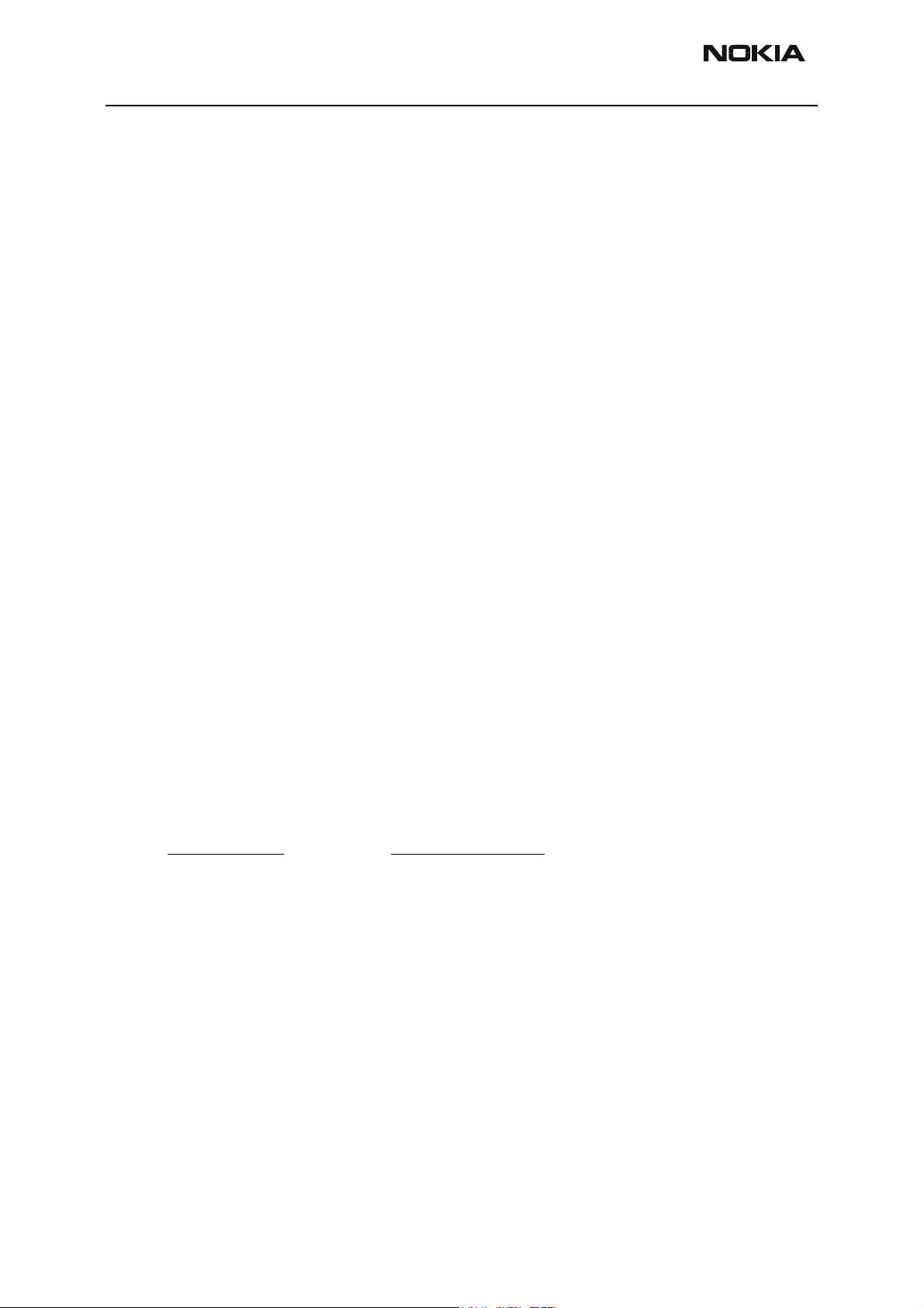
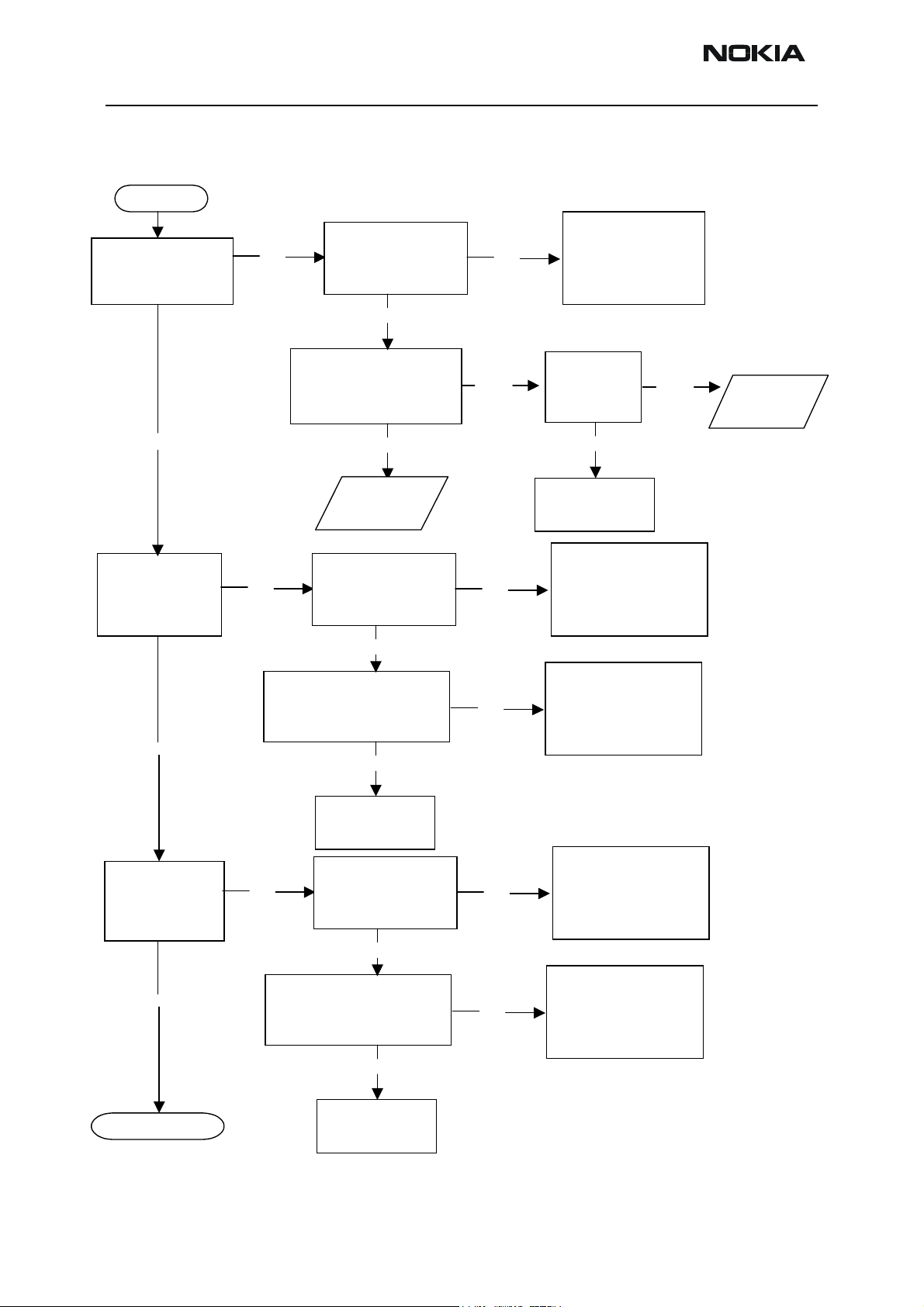
Phone is Dead
Start
Is phone
current 0 mA?
No
Replace
R204
Will the phone
es
power-up in
Test or Local
mode?
Check BSI
No
circuit R204
OK?
With the phone in
LOCAL mode, using
Phoenix check battery
voltage, recalibrate if
necessary.
Is flash
programming
working?
No
es
es
es
Check X200
No
(contact and
solder joints).
OK?
Are VFLASH1 and
IO enabled
momentarily at
power up?
es
Check RF-CLK
at both sides
of C300. Is it
19.2MHz?
es
Possible
problem with
TIKU, UEME, or
Memories.
No
es
No
X200
Replace
UEME
D200
Check R822,
No
C300, C861,
Replace
C870 and
L899.
OK?
es
Replace
G820
No
Replace
defective
part.
Flash fault
End
Issue 1 (11/2003) Copyright 2003 Nokia Corporation Page 6-5
Company Confidential
Page 6
NMM-3 Company Confidential
p
Y
Y
Y
Y
Y
Y
6-Troubleshooting CCS Technical Documentation
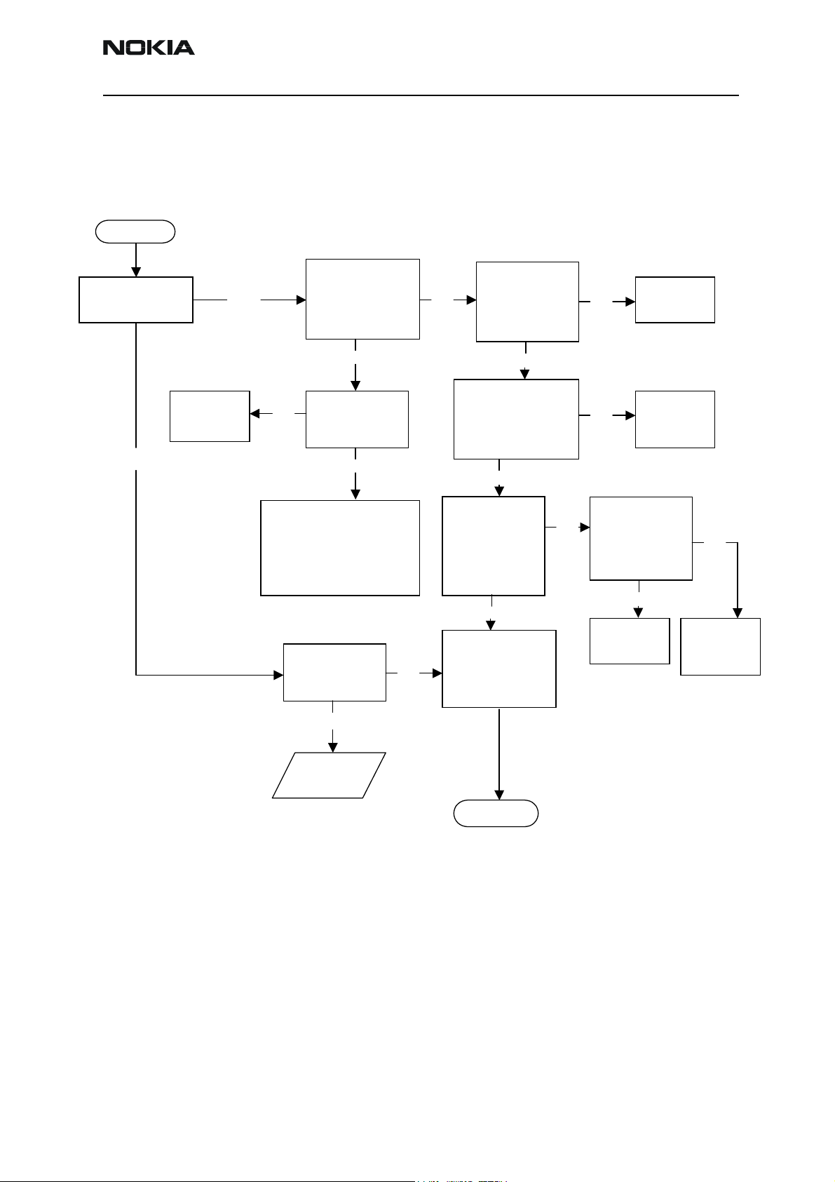
Flash Programming Fault
Start
Is the FBUS TXline HIGH after
startu
?
es
Is FBUS TX-line set
LOW after it has
been HIGH?
No
Measure BSIpulse during
flash operation.
OK?
Measure FBUS
TX-line during
flashing. Is it
~1.8V?
No
es
es
Check BSI circuit
No
including X200,
R204, R209, R214
and C226. OK?
No
Replace TIKU
D300
Check R403, if
OK replace
UEME D200.
es
Wrong
manufacture ID
and device ID
No
Possible short
circuit under TIKU
or program flash.
Replace or reflow
devices, Retest. OK?
es
End (reset)
es
No
Replace
Program
Flash D451
Phone is
dead
Page 6-6 Copyright 2003 Nokia Corporation Issue 1 (11/2003)
Company Confidential
Page 7
Company Confidential NMM-3
Y
V
Y
Y
Y
CCS Technical Documentation 6-Troubleshooting
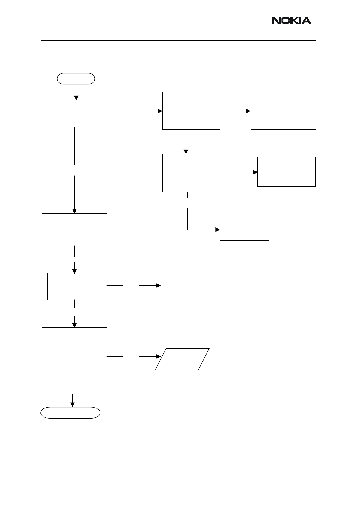
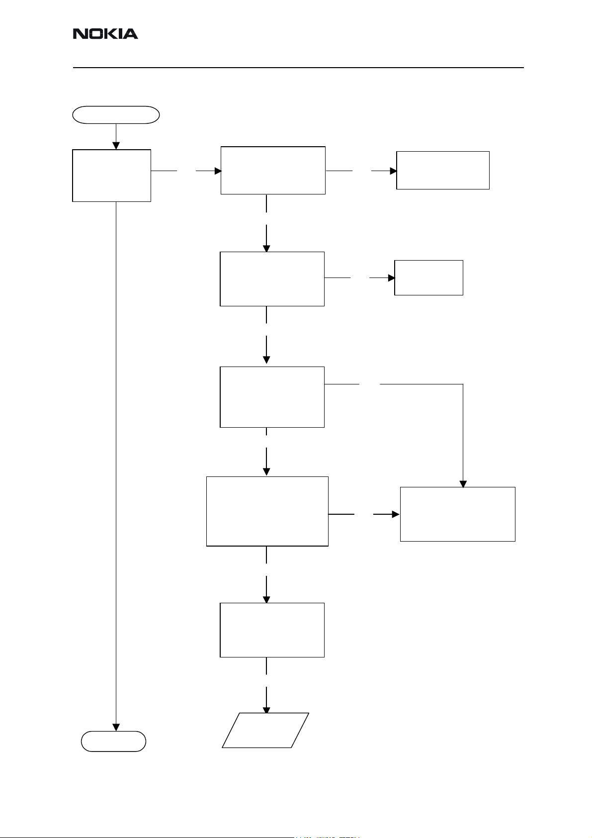
SIM Card Fault (Insert SIM / Card Rejected)
Start
Check SIM connector
makes good contact
to SIM X405. OK?
es
Set phone to
LOCAL mode. Is
it OK?
es
Measure VSIM
oltage on C405.
Is it ~3.0V?
No
No
No
Replace SIM
connector X405
Check BSI circuit
including X200, R204,
R209, R214 and C226.
If OK replace UEME
Measure FBUS
TX-line during
flashing. Is it
~1.8V?
es
Check SIM
power-up
sequence. Is it OK
es
Replace TIKU
D300
End
No
Check SIM lines, if
OK replace UEME
D200.
Issue 1 (11/2003) Copyright 2003 Nokia Corporation Page 6-7
Company Confidential
Page 8
NMM-3 Company Confidential
p
g
Y
Y
Y
Y
µ
Y
Y
µ
Y
Y
Y
Y
6-Troubleshooting CCS Technical Documentation
Keypad Fault
Start
Is the power key
working?
es
Is the volume
up key
working?
No
Measure voltage
No
on S400 is it
hi
h?
Measure Voltage on
S400 when pressed.
Is it high?
Phone is
dead
Measure ROW5
line from S402.
Is it ~1.8V?
No
es
es
No
No
Check R432, R40
and R439 and
line, if OK,
lace UEME.
re
Check
S400 is
OK?
No
Replace S400
Check S402, R400
and R438, if it still
fails replace TIKU
D300.
es
Phone is
dead
es
Is the volume
down key
working?
es
es
Measure COL1 from
S402, when pressed, is
there a 50
s pulse?
es
Replace TIKU
D300
Measure ROW5
No
line from S403.
Is it ~1.8V?
es
Measure COL0 from
S402, when pressed, is
there a 50
s pulse?
es
No
No
No
Check S402, R400
and R436, if it still
fails replace TIKU
D300.
Check S403, R400
and R438, if it still
fails replace TIKU
D300.
Check S403, R400
and R437, if it still
fails replace TIKU
D300.
Continue
Replace TIKU
D300
Page 6-8 Copyright 2003 Nokia Corporation Issue 1 (11/2003)
Company Confidential
Page 9
Company Confidential NMM-3
g
Y
Y
Y
j
Y
CCS Technical Documentation 6-Troubleshooting
Continue
Are the UImodule keys
working?
No
Replace the UImodule. Are keys
workin
now?
No
Check X400 solder
oints and spring
contacts. OK?
es
Measure ROW0 –
ROW5 lines from
X400. Are voltage
levels ~1.8V?
es
No
es
Retest the faulty
UI-module.
Replace
X400
No
End
Measure SLEEPX signal
on testpoint J301
when a key is pressed.
Is voltage level ~1.8V?
es
When a key is
pressed, do the
LED’s illuminate?
No
Illumination
Fault
No
Check ROW0 – ROW5
lines from X400. If OK
replace TIKU.
Issue 1 (11/2003) Copyright 2003 Nokia Corporation Page 6-9
Company Confidential
Page 10
NMM-3 Company Confidential
j
V
V
g
Y
Y
Y
Y
6-Troubleshooting CCS Technical Documentation
Display Fault
Start
Replace display
module. Does the
display now work?
No
Check X400 and UI
connector X3
contacts and solder
oints. OK?
es
Measure VIO (1.8V)
and VFLASH1 (2.7V) at
X3. are they OK?
No
es
No
Replace display
module.
Replace
defective part.
Check
continuity of
IO and
FLASH1, and
es
Check for activity on
data, address, and WRX
lines and the RESX line
on power up. OK?
es
Are Display
LEDs
illuminatin
End
No
No
Replace TIKU
D300.
Illumination
Fault
Page 6-10 Copyright 2003 Nokia Corporation Issue 1 (11/2003)
Company Confidential
Page 11

Company Confidential NMM-3
V
Y
Y
X
Y
Y
Y
X
Y
Y
V
Y
Y
CCS Technical Documentation 6-Troubleshooting
Illumination Fault
Start
Are the display
LED’s working?
es
Are the keypad
LED’s working?
No
No
Replace display module.
Do lights work?
No
Measure voltage on
400 Cathode.
~
Check V400 and
L400. Are they OK?
es
Replace UI-module. Do
lights work?
es
Replace Display
Check X400 and
3 contacts and
~
solder joints.
OK?
No
Replace
defective part.
es
Replace
N400
Replace
No
defective part.
Replace
N400
es
Replace
Keypad
LEDs
End
No
Measure voltage on
R426. Is it ~2.2V?
es
Retest
Replace
N400
Check X400 and
No
es
solder joints.
OK?
Measure voltage on
400 Cathode. Is
~10.5V?
Check V400 and L400.
Are they OK?
3 contacts and
es
it
No
No
No
es
Replace
defective part.
Replace
N402
Replace
defective part.
Issue 1 (11/2003) Copyright 2003 Nokia Corporation Page 6-11
Company Confidential
Page 12

NMM-3 Company Confidential
Y
Y
Y
Y
6-Troubleshooting CCS Technical Documentation
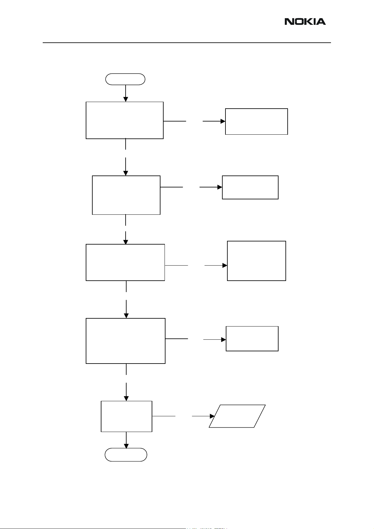
Charger Fault
Start
Is charger rejected
when connected.
es
Use Phoenix to
read BTEMP.
~Ambient?
es
Using Phoenix with
the JBV-1 recalibrate
battery voltage and
charger current and
voltage.
No
No
Check X402,
F400, L402, V403,
C410, R200 and
C411. OK?
Check BTEMP
circuit including
X210, R211 and
C227. OK?
es
No
No
Replace
defective part.
Replace UEME
D200.
es
Replace
defective part.
End
Page 6-12 Copyright 2003 Nokia Corporation Issue 1 (11/2003)
Company Confidential
Page 13

Company Confidential NMM-3
j
y
Y
Y
Y
Y
Y
Y
Y
CCS Technical Documentation 6-Troubleshooting
Accessory Fault
Measure ACI line
(pin 3). Is it ~0V?
es
Measure VOUT
(pin4) Is it ~2.8V?
Non ACI-Accessory
No No
No
Start
Check system
connector X401
contacts and solder
oints. OK?
es
Check ACI line,
L4??, R429, R409.
If faulty, replace
defective part
and retest.
Check L4??
and R409.
OK?
No
ACI-Accessor
No
Replace
defective part.
Repair or replace
system connector.
Look for activiy on
the ACI line on
initial accessory
connection.
es
Check L405-L407,
C416-C419 and
R421. OK?
es
Replace UEME
Replace
UEME D200.
In a call, check
In a call, check
operation of
operation of XEAR
and XMIC.
No
Replace
defective part.
es
No
es
No XMICNo XEAR
Check L404, L403,
R415, C412 and
C413. OK?
es
Replace UEME
End
Issue 1 (11/2003) Copyright 2003 Nokia Corporation Page 6-13
Company Confidential
Page 14

NMM-3 Company Confidential
Y
Y
Y
6-Troubleshooting CCS Technical Documentation
Audio Fault
Does hands free
work?
es
Check contacts and
solder joints of UI
connector X400 and
earpiece connector,
replace earpiece if
necessary. OK?
es
No
No
Start
Is the problem with the
Uplink or Downlink?
TIKU or UEME
Fault
Replace
defective
part
No
UplinkDownlink
Measure MIC
Bias voltage
across R104, is it
~2.1V?
es
Check Microphone and
contacts, R103, R104, R105,
C103, C104 and L102
replace defective part.
Is the DC bias
voltage at R405
and R406 ~1.35V?
No
Replace
UEME
End
Page 6-14 Copyright 2003 Nokia Corporation Issue 1 (11/2003)
Company Confidential
Page 15

Company Confidential NMM-3
Y
Y
Y
Y
CCS Technical Documentation 6-Troubleshooting
Camera Fault
Start
Is ‘Operation Failed’
message returned
when the camera is
selected?
es
Check camera
module is fitted
correctly and
contacts are OK?
es
In view finder
mode, check VOUT
on N102 is ~1.8V
No
No
No
Replace camera
module.
Replace or refit
camera module.
Replace
regulator N102
es
In view finder
mode, check for
activity on signal
and clock lines.
es
Replace camera
module.
End
No
Replace TIKU
D300
Issue 1 (11/2003) Copyright 2003 Nokia Corporation Page 6-15
Company Confidential
Page 16

NMM-3 Company Confidential
Y
Y
Y
Y
Y
6-Troubleshooting CCS Technical Documentation
USB Fault
Start
Connect a USB device
to phone and check
N401 Vpu goes to 3.3V.
es
Is there any
activity on
D+ and D-?
No
Check R423, R424,
R410, R413 and
X410. OK?
es
es
No
Check VCC
for ~5V
es
No
Check R442, L411,
C414 and X401.
Replace if defective.
No
Replace
defective part.
Replace N401.
OK?
es
End
No
Replace
TIKU
Page 6-16 Copyright 2003 Nokia Corporation Issue 1 (11/2003)
Company Confidential
Page 17

Company Confidential NMM-3
CCS Technical Documentation 6-Troubleshooting
GSM900/1800 TX Troubleshooting
Phoenix Settings:
Band = GSM900/GSM1800
Active Unit = Tx
Op Mode = Burst
Tx Chan = 37 GSM900
Pwr Lvl = 5
Tx Chan = 700 GSM1800
Pwr Lvl = 0
PA Mode = Free
Tx Data Type = Random
Tx OK
Yes
Yes
Check output signal level
from antenna conncetor
+32.5dBm @ 897.4MHz (GSM900)
+29.5dBm @ 1747.8MHz (GSM1800)
OK ?
No
Tx signal found ?
Yes
Check with RF probe signal
level on PA input
+0dBm on 900 PA i/p
-1dBm on 1800 PA i/p
OK ?
Yes
Start Tx power level tuning
and check tuned DAC values:
Highest level ~700 (GSM900)
Highest level ~600 (GSM1800)
Lowest level ~170
Base level ~150
Major differences ?
No
Yes
No
Check all
power levels
OK ?
Check output signal
on 500MHZ span
Signal found on
correct frequency ?
Check Tx filter/
Tx balun input level
-4dBm on 900 FILT i/p
-4dBm on 1800 BALUN i/p
Replace faulty
component
Yes
Yes
OK ?
Yes
Tune TX DAC
No
values
Tune Tx
power levels
OK ?
No
Yes
No
No
Synthesizer
troubleshooting
HELGO
troubleshooting
No
Check with oscilloscope
900 & 1800 PA CONTROL
VPCTRL >1.5V max
C564/C565
OK ?
Yes
PA & ant. switch
troubleshooting
No
Check power control
loop components
OK ?
No
Replace faulty
component
Yes
Replace HELGO
Issue 1 (11/2003) Copyright 2003 Nokia Corporation Page 6-17
Company Confidential
Page 18

NMM-3 Company Confidential
Y
Y
V
Y
V
V
V
Y
6-Troubleshooting CCS Technical Documentation
HELGO Troubleshooting
Phoenix Settings:
Band=GSM900
Active Unit=Tx
Op Mode=Burst
Tx Chan=37
PA Mode=Free
Pwr Lvl=19
es
Check with scope/multimeter
TXI/TXQ Signals
R2,VR3,VR4,VR5,=2.8V
R1A=4.8V
REF01=1.35V
HELGO
HELGA serial interface
TXP & TXC signals
OK?
No
Baseband
Troubleshooting
es
Check with RF FET Probe:
CO Output signal
3589.6Mhz CH37 (GSM900)
3495.6MHZ CH700 (GSM1800)
Level>-10dBm
OK?
es
Check modulator output
components
OK?
No
Replace faulty
components
No
Synthesizer
Troubleshooting
es
Replace Helgo
Page 6-18 Copyright 2003 Nokia Corporation Issue 1 (11/2003)
Company Confidential
Page 19

Company Confidential NMM-3
CCS Technical Documentation 6-Troubleshooting
PA and Antenna Switch Troubleshooting
Check with RF probe
+4dBm 900MHz
-4dBm 1800MHz
OK ?
Yes
Check with oscilloscope:
VBatt = 3.8V
VCC1 = VCC2 = VCC3 = 3.8V
VTXLO-G= 2.8V pulse (0V GSM1800)
VTXB-G= 2.8V pulsed (0V GSM1800)
VTXB-D= 2.8V pulsed (0V GSM900)
OK ?
Yes
No
Replace PA
Yes
Check with oscilloscope:
Check Ant Switch
GSM VANT-2 = 2.6V pulse
GSM VANT-1 = 2.6V pulse
OK ?
No
Check VANT line components
L638/L639/C551/352
OK ?
Yes
Yes
Replace ant.
switch
No
Replace faulty
component
Check components
around PA
OK ?
No
Replace faulty
component
Yes
Replace HELGO
Issue 1 (11/2003) Copyright 2003 Nokia Corporation Page 6-19
Company Confidential
Page 20

NMM-3 Company Confidential
Y
Y
V
V
Y
Y
YesY
Y
V
YesY
6-Troubleshooting CCS Technical Documentation
GSM900 RX Troubleshooting
Phoenix Settings:
Band:GSM900
Active unit:RX
Op Mode:Continuous
Rx/Tx Chan:37
AGC:maximum (default)
Apply a –85dBm
942.46771MHz signal
from generator to RF
connector
Check C575 &
RF connector
Scope at
GRXI/GRXQ
Signal 1.3Vpp
DC Offset=1.2V
Freq=67.7KHz
900MHz chain
functional
es
es
No
Spectrum
analyser
CO output
3769.6MHz
-20dBm
No
Synthesizer
troubleshooting
es
Change
generator
level to
–50dBm
es
Is spectrum analyser
Ant Switch output
-53dBm?
Spectrum analyser
Helgo Inputs
-54dBm
Check
Helgo
No
Spectrum analyser
ant switch Input
-51dBm
No
No
No
Scope
ant_1 =0V
In Rx mode
Check
ant switch
Check
L633,L634
es
es
Check
R2,VR3,VR4,VR5=2.8V
Helgo serial interface
No
Baseband
Troubleshooting
es
HELGO
Troubleshooting
Page 6-20 Copyright 2003 Nokia Corporation Issue 1 (11/2003)
Company Confidential
Page 21

Company Confidential NMM-3
Y
Y
Y
V
V
Y
Y
YesY
Y
V
YesY
CCS Technical Documentation 6-Troubleshooting
GSM1800 RX Troubleshooting
Phoenix Settings:
Band:GSM1800
Active unit:RX
Op Mode:Continuous
Rx/Tx Chan:700
AGC:maximum (default)
es
Apply a –85dBm
1842.86771MHz signal
from generator to RF
connector
es
Scope at
GRXI/GRXQ
Signal 1.3Vpp
DC Offset=1.2V
Freq=67.7KHz
es
1800MHz
Chain
Functional
No
Spectrum
analyser
CO Output
3685.6MHz
-20dBm
No
Synthesizer
troubleshooting
es
Change
generator
level to
–50dBm
es
Is spectrum analyser
ant switch output
-54dBm?
Check
Helgo
Check C575 &
RF connector
No
Spectrum analyser
ant switch input
-51dBm
Scope
No
ant_1 =0V
In Rx mode
es
es
Spectrum analyser
Helgo inputs
-55dBm
Check
R2,VR3,VR4,VR5=2.8V
Helgo serial interface
es
HELGO
Troubleshooting
No
No
Check
Ant Switch
Check
L635,L636
Baseband
Troubleshooting
Issue 1 (11/2003) Copyright 2003 Nokia Corporation Page 6-21
Company Confidential
Page 22

NMM-3 Company Confidential
V
V
V
V
g
V
V
Y
Y
YesY
Y
Y
V
V
Y
Y
Y
Y
6-Troubleshooting CCS Technical Documentation
GSM900/1800 Synthesizer Troubleshooting
Pheonix Settings:
Band:GSM900/1800
Active unit:RX
Op Mode:Continuous
Rx Chan:37/700
AGC:maximum (default)
es
Probe VCO o/p
3769.6MHz GSM900
3685.6MHz GSM1800
Span 1MHz
RF Level=-10dBm
No
CO output signal
<-10dBm?
No
Check output signal on
1GHz Span. Signal found
on correct frequency?
No
es
Check Balun output
es
& VCO solder joints
OK?
es
Synth
OK
es
Replace
CO
Check VCO
cc=2.8v
No
Baseband
Troubleshootin
No
Replace faulty
components
Replace
CO
Check with meter VCO
control voltage
c=0V?
No
CO control
voltage>4V
es
Check VCO loop
filter components
OK?
No
Replace faulty
components
es
Check synth serial
Interface on Helgo
es
Replace
CO
No
Helgo
Troubleshooting
es
Replace
CO
Page 6-22 Copyright 2003 Nokia Corporation Issue 1 (11/2003)
Company Confidential
Page 23

Company Confidential NMM-3
Y
Y
YesY
Y
Y
V
V
V
p
YesY
Y
CCS Technical Documentation 6-Troubleshooting
WCDMA Tx Troubleshooting
Phoenix Settings:
Tx Contol (WCDMA)
Algorithm mode
Start Level =21dBm
Channel=9750 (1950MHz)
Click SEND
es
Check o/p signal level
From RF connector
21dBm @ 1950MHz
No
TX Signal Found?
es
Check with RF probe
level at PA Input
(C984)
-3dBm
es
Tx
OK
No
Check output signal on
500MHz Span signal
found on incorrect
frequency?
No
Check WCDMA Tx
balanced filter input
(L959)
-4dBm
WCDMA Measurement settings:
RBW=30khz VBW=300khz, detector:sample,
CSP=5MHz,CBW=3.84MHz
RFProbe with 10:1 attenuator
Synthesizer
Troubleshooting
Check WCDMA Hex
es
balanced filter input
(R955 pads)
=-17dBm
es
Tx
OK
PA and DC-DC
Converter
Troubleshooting
es
No
Replace
Filter
No
Check TXA2 Volt drop
across R906.
DAC=800
≈ 80mV
No
Baseband
Troubleshooting
es
Check DC conditions
On Hex.
CCTC=VPLUS=
CCOUT =VCCBIAS
=2.8v
Check components
No
around Hex
OK?
No
Replace
faulty
com
onents
Replace
HEX
Issue 1 (11/2003) Copyright 2003 Nokia Corporation Page 6-23
Company Confidential
Page 24

NMM-3 Company Confidential
Y
Y
YesY
Y
p
Y
Y
Y
V
V
6-Troubleshooting CCS Technical Documentation
PA and DC-DC Converter Troubleshooting
Check with RF probe
Signal level at PA input
-3dBm?
es
Check Ireg voltage
(C980)1.3v?
es
Check VREG=2.8v
Check detector
voltage (C960)
0.6v<V<1.5v
es
es
No
Check R965 & R967
OK?
es
Check coupler,
es
isolator & duplexer
OK?
Check DC-DC Converter
enable
bat=3.6v (C387)
CC1 & VCC2 ≥1.5v
No
No
Check components
around DC-DC
converter OK?
Replace
Faulty
component
Change
PA
Replace faulty
com
onents
No
es
Replace DC-DC
converter
No
Check components
around detector
circuit OK
No
Replace
faulty
component
No
Replace
faulty
component
Page 6-24 Copyright 2003 Nokia Corporation Issue 1 (11/2003)
Company Confidential
Page 25

Company Confidential NMM-3
Y
Y
Y
Y
Y
Y
Y
Y
CCS Technical Documentation 6-Troubleshooting
WCDMA Rx Troubleshooting
Phoenix Settings:
Phoenix Settings:
Rx Control (WCDMA)
Rx Contol (WCDMA)
AGC mode = Manual
AGC mode =Manual
AFC algorithm = Off
AFC algorithm=Off
Channel = 10700 (2140MHz)
Channel=10700 (2140MHz)
BB AGC = 33dB
Click SEND
Click SEND
es
Apply a –48dBm
2141MHz CW signal
from generator to
WCDMA RF connector
es
Scope probe on RXI/RXQ
lines R844/R845 400mVpp
DC offset 700mV
FET Probe R845/R845
Freq=1MHz
RF Level =-7dBm
es
WCDMA RX
Chain OK
Replace
SAW Filter
No
No
Probe on Rx VCO
output 4280MHz
Level ≈ -17dBm
es
Signal on
balun input
-54dBm
es
Signal on balun
diff output
C890/C892
-57dBm
es
Signal level at output of LNA
C811.
Manual Mode in Phoenix
Low gain=-70dBm
Mid Gain=-55dBm
High gain =-44dBm
es
No
No
No
Troubleshooting
Replace
Duplexer
Replace Balun
No
Synthesizer
Check VR4
2.8v
No
Baseband
Troubleshooting
Check signal level at SAW
Filter output C844
-45dBm
OK?
No
Replace C842 and/
or C844
es
Replace
REX
Issue 1 (11/2003) Copyright 2003 Nokia Corporation Page 6-25
Company Confidential
Page 26

NMM-3 Company Confidential
V
V
V
YesY
YesY
Y
YesY
Y
Y
Y
6-Troubleshooting CCS Technical Documentation
WCDMA Rx Synthesizer Troubleshooting
Phoenix Settings:
Rx Contol (WCDMA)
AGC mode = Manual
AFC algorithm= Off
Channel= 10700 (2140MHz)
Click SEND
es
Probe VCO output
4280MHz
Span 1MHz
RF Level= -17dBm
No
CO o/p signal
<-17dBm?
No
Check output signal on
1GHz Span. Signal found
on correct frequency?
No
es
Synth
OK
Check balun output
& VCO solder joints
OK?
es
Replace
VCO
es
Check VCO
cc= 2.8v
No
Baseband
Troubleshooting
No
Replace faulty
components
Replace
VCO
Check with meter VCO
control voltage R802=
0V?
No
CO control
voltage >4V
es
Check VCO loop
filter components
OK?
No
Replace faulty
components
es
Check synth serial
interface on Rex
Replace
VCO
No
Rex
Troubleshooting
es
Replace
VCO
Page 6-26 Copyright 2003 Nokia Corporation Issue 1 (11/2003)
Company Confidential
Page 27

Company Confidential NMM-3
V
V
YesY
YesY
Y
YesY
Y
Y
CCS Technical Documentation 6-Troubleshooting
WCDMA Tx Synthesizer Troubleshooting
Phoenix Settings:
Tx Contol (WCDMA)
Algorithm mode
Start Level = 0dBm
Channel= 9750 (1950MHz)
Click SEND
Probe VCO o/p
3900Mhz
Span 1MHz
RF Level= -17dBm
No
CO o/p signal
<-17dBm?
No
Check o/p signal on 1GHz
Span. Signal found on
correct frequency?
No
es
Synth
OK
Check balun output
& VCO solder joints
OK?
es
Replace
VCO
es
Check
cc= 2.8v
ExtReg1
No
Baseband
Troubleshooting
No
Replace faulty
components
Replace
VCO
Check with meter VCO
control voltage R914=
0V?
No
VCO control
Voltage >4V
es
Check VCO loop
filter components
OK?
No
Replace faulty
components
es
Check synth serial
interface on Tex
Replace
VCO
No
Tex
Troubleshooting
es
Replace
VCO
Issue 1 (11/2003) Copyright 2003 Nokia Corporation Page 6-27
Company Confidential
Page 28

NMM-3 Company Confidential
N
N
N
6-Troubleshooting CCS Technical Documentation
GSM/WCDMA Antenna Troubleshooting
Replace
WCDMA
antenna
Test Points
Yes
Antenna
spring
contacts
OK?
o
Replace
faulty
contacts
O WCDMA
Ground
antenna
connection
Phone in mechanics
with C (battery) and D
(antenna) covers
With multimeter check GSM &
WCDMA antennas make
ground connection with battery
connector ground
OK?
Yes
GSM & WCDMA
antenna OK
O GSM
ground
antenna
connection
Replace
antenna
module
Signal Ref Test point Function Characteristic Note
PURX 100 N101 Pin 44 External reset 1.8V Active Low From UEME
SLEEPX 101 J101 Sleep mode control signal 1.8V Active mode
0V Sleep mode
SLEEPCLK 102 N101 Pin 26 Sleep Clock 32.768KHz digital clock
1.8V
UEMRSTX 103 N101 Pin 49 UEME Reset Vbat
SYSCLK 104 N101 Pin 50 Bluetooth system Clock 26MHz
CBUSCLK 105 N101 Pin 36 Serial control bus clock 1MHz digital clock signal
1.8V
CBUSDA 106 N101 Pin 35 Serial control bus data bi-
1.8V digital signal bi-directional
directional
CBUSENX 107 N101 Pin 34 CBUS enable signal 1.8V digital signal
MICBI 108 R103 Microphone bias voltage 2.1V
MIC1P 109 C103 Microphone positive ~1.35V dc + signal
MIC!N 110 C104 Microphone negative ~1.35V dc
Internal Mic 111 L12 Microphone out 1V - 2V + signal Depending on microphone
LEDA 112 R106 Anode supply for Infrared Vbat IR Off
~Vbat - 1.6V IR on digital
signal
TXD 113 V100 Pin 3 Infrared Tx data 1.8V digital signal
RXD 114 V100 Pin 4 Infrared Rx data 1.8V digital signal
VOUT 115 C109 Camera supply 2.8V
CAMSWITCH 116 R110 Camera switch 1.8V
FBUSRX 400 J400 Pin 3 Flash programming data
2.78V digital signal From FPS-8 / PC to phone
and phone control
TIKU peripheral control
bus
Page 6-28 Copyright 2003 Nokia Corporation Issue 1 (11/2003)
Company Confidential
Page 29

Company Confidential NMM-3
CCS Technical Documentation 6-Troubleshooting
Signal Ref Test point Function Characteristic Note
FBUSTX 401 J400 Pin 2 Flash programming data
and phone control
MBUS 402 J400 Pin 7 Flash programming clock 2.78V digital signal 6.5
COL2 403 R435 Key pad column 1.8V digital signal
COL1 404 R436 Key pad column 1.8V digital signal
COL0 405 R437 Key pad column 1.8V digital signal
ROW5 406 R438 Key pad row 1.8V digital signal
+VLCDLED 407 V400 Cath-
ode
-VLCLED 408 R408 LCD LED current sense ~0.5V
KLIGHT 409 N402 Pin 2 Key LED control signal Vbat Active low
DLIGHT 410 N400 Pin 8 Display LED control signal Vbat Active high
1KEYLED 411 R426 Key light current sense
SIMDATA 412 X403 Pin 6 SIM data 1.8V / 3V digital signal From UEME to SIM card
SIMCLK 413 X403 Pin 1 SIM Clock 1.8V / 3V digital signal From UEME to SIM card
SIMRST 414 X403 Pin 2 SIM Reset 1.8V / 3V digital signal From UEME to SIM card
HOOKINT 415 J407 Accessory off hook inter-
ACI 416 C425 Accessory detection and
VBUS 417 C422 USB external supply in
Vreg 418 C414 USB IO supply 3.3V
D+ 419 C421 USB data 3.3V digital signal 12MHz
D- 420 C424 USB data 3.3V digital signal 12MHz
XMICN 421 L404 External microphone neg-
XMICP 422 L403 External microphone posi-
XEARN 423 L405 External ear negative left /
XEARP 424 L406 External ear positive left /
XEARNR 425 L407 External ear negative right 1.35V dc - signal
XEARPR 426 L408 External ear positive right 1.35V dc + signal
VCHAR 427 V403 Cath-
ode
CLK 450 J450 SDRAM Clock 1.8V digital signal
FlsCLK 451 J451 Flash Clock 1.8V digital signal
VOUT 452 C451 SDRAM Supply voltage 2.85V
VPP 453 C453 Flash programming volt-
OUT 300 C301 COWIS regulator out 1.8V
RFCKOCK 301 C300 Reference Clock 19.2MHz
Supply for Key and LCD
LEDs
resistor
rupt signal
digital communications
bus
from host
ative
tive
mono
mono
Charger voltage ~4.2V charging
age
2.78V digital signal From phone to FPS-8 / PC
MHz max
~10.5V 18V max open circuit
~1.9V
2.8V no accessory
1.8V accessory connected
1.1V button pressed
2.78V digital sinal Bidirectional data
~5.0V
0V no accessory con-
nected
2.1V no accessory con-
nected
1.35V dc - signal
1.35V dc + signal
~8.0V charge switch open
1.8V Internal
12V External
Value with accessory connected varies with accessory type.
Value with accessory connected varies with accessory type.
When:
Ibat = 500mA
Vbat = 3.8V
FPS-8 external VPP source
Issue 1 (11/2003) Copyright 2003 Nokia Corporation Page 6-29
Company Confidential
Page 30

NMM-3 Company Confidential
6-Troubleshooting CCS Technical Documentation
Signal Ref Test point Function Characteristic Note
FBUSRXI 302 J313 Flash programming data
and phone control
FBUSTXI 303 J314 Flash programming data
and phone control
MBUSRX 304 J315 Flash programming clock 1.8V digital signal From UEME to TIKU
MBUSTX 305 J316 ACI data bus between
UEME and TIKU
OSCIN 200 C211 Real Time Clock crystal in 32.768KHz
OSCOUT 201 C210 Real Time Clock crystal
out
VBAT 202 J202 Battery voltage 3.2V - 4.2V
BSI 203 J203 Battery size indicator
Local mode indicator SIM
removal Indicator Flash
programming start signal
BTEMP 204 R211 Battery temperature indi-
cator
VTIKU 205 C203 TIKU core supply voltage 1.5V
VANA 206 C208 UEME internal analog
supply
VFLASH1 207 C208 LDO regulator 2.78V
VAUX2 208 C207 Accessory supply 2.78V
VCORE 209 C207 Camera digital supply 1.8V
VIO 210 C206 I/O supply 1.8V
VSIM 211 C206 Programmable SIM card
supply
PAOUTP 212 R227 Handsfree speaker posi-
tive
PAOUTN 213 R228 Handsfree speaker nega-
tive
VIBRA 214 X207 Pulsed vibra drive voltage Vbat Off
VR1A 215 C241 GSM / WCDMA RF supply 4.75V
VR1B 216 C236 WCDMA Tx supply 4.75V
VR2 217 C234 GSM / WCDMA Tx supply 2.78V
VR3 218 C235 TCXO supply 2.78V
VR4 219 C233 GSM / WCDMA Rx supply 2.78V
VR5 220 C235 GSM / WCDMA Rx supply 2.78V
VR6 221 C234 WCDMA Rx VCO supply 2.78V
VR7 222 C233 GSM VCO supply 2.78V
SMPSCLK 223 J201 VTIKU regulator mode
select
1.8V digital signal From UEME to TIKU
1.8V digital signal From TYIKU to UEME
1.8V digital signal Bi-directional
32.768KHz
1.2V in normal mode
0.09V in local mode
If BSI line rises >2.1V,
2.78V BSI pulse
~0.9V at 25ºC
2.78V
1.8V or 3.0V Voltage determind by SIM
Vbat/2 + signal When active
Vbat/2 - signal When active
~Vbat - 1.5V On
2.8V active mode
0V sleep mode
To UEME A/D converter
type
Page 6-30 Copyright 2003 Nokia Corporation Issue 1 (11/2003)
Company Confidential
Page 31

Company Confidential NMM-3
CCS Technical Documentation 6-Troubleshooting
Calibration required when components changed
Table 1: Baseband Components
Component ID NMP Code Description Calibration required
D200 4370945 UEME V2.0 Energy management calibration, GSM calibration
R200 1414605 CHIPRES 0R22 Charge calibration
R209 1430187 CHIPRES 100K 1% BSI calibration
D451 4341497 8Mx16 FLASH Energy management calibration
WCDMA/GSM calibration
435C067 Bluetooth Reflash BT-NO CAL
Table 2: WCDMA Component Alignment
WCDMA
TUNINGS
REX (N810) NO YES YES YES NO NO NO NO
RX SAW
(Z800)
RX VCO
(G800)
TEX (N900) NO YES NO NO YES YES NO YES
HEX (N902) NO NO NO NO YES YES NO NO
PA (N960) YES NO NO NO YES YES YES NO
TX VCO
(G900)
Isolator
(Z962)
TX SAW
(Z900)
Duplexer
(Z960)
Power
Detector
Cal
NO NO NO YES NO NO NO NO
NO NO NO NO NO NO NO ON
NO NO NO NO NO NO NO ON
YES NO NO NO YES YES NO NO
NO NO NO NO YES YES NO NO
YES NO YES YES YES YES NO NO
RF Channel
Filter Cal
Rx AGC
Alignment
Table 3: GSM Component Alignments
Rx Band
Response
Cal
Tx AGC
Alignment
Tx Band
Response
Cal
Tx PA Bias
Tuning
Temperatu
re Sensor
Cal
GSM TUNINGS Rx Channel
Select
Filter Cal
HELG0 (N600) YES YES YES YES YES YES
PA (N550) NO NO NO NO YES YES
ANT SW (Z500) NO YES YES YES YES YES
VCO (G650) NO NO NO NO YES NO
TX SAW (Z650) NO NO NO NO NO NO
Rx Cal
Rx Band
Filter
Response Cal
Rx DtoS
Balance Cal
Tx IQ Tuning
Tx Power
Level Tuning
Issue 1 (11/2003) Copyright 2003 Nokia Corporation Page 6-31
Company Confidential
Page 32

NMM-3 Company Confidential
6-Troubleshooting CCS Technical Documentation
This page has been deliberately left blank
Page 6-32 Copyright 2003 Nokia Corporation Issue 1 (11/2003)
Company Confidential
 Loading...