

Page 1

Customer Care Solutions
NMM-3 Series Transceivers
7 - System Module & UI
Issue 1 (11/2003) Copyright 2003 Nokia Corporation Page 7-1
Company Confidential
Page 2

NMM-3 Company Confidential
7 - System Module & UI CCS Technical Documentation
Table of Contents
Page No
Introduction ............................................................................................................................................. 5
System Module Baseband .................................................................................................................... 5
Power Distribution Diagram ..............................................................................................................7
Environmental operating conditions ...............................................................................................8
Temperature Conditions................................................................................................................... 8
Humidity and Water Resistance.................................................................................................... 8
Baseband Functional Description ...................................................................................................... 8
Modes of Operation ............................................................................................................................. 8
Battery .....................................................................................................................................................9
Backup Battery ....................................................................................................................................10
Power Up and Reset ...........................................................................................................................10
UEME Reset Sequence and Timings ..............................................................................................11
A/D Channels .......................................................................................................................................11
ZOCUS ....................................................................................................................................................12
Bluetooth ..............................................................................................................................................13
Camera ..................................................................................................................................................15
UI Module .............................................................................................................................................16
Display ................................................................................................................................................. 16
Backlighting .................................................................................................................................... 16
IR Module .............................................................................................................................................18
SIM Interface .......................................................................................................................................19
External Accessory Interface ...........................................................................................................20
Pop-Port System Connector ........................................................................................................ 20
Charger interface............................................................................................................................ 21
ACI ..................................................................................................................................................... 21
USB interface................................................................................................................................... 21
External Audio ................................................................................................................................... 22
External Microphone Connection ............................................................................................. 22
External Earphone Connections ................................................................................................ 23
Internal Audio .................................................................................................................................... 23
IHF Speaker ..................................................................................................................................... 23
Internal Microphone ..................................................................................................................... 24
Internal Speaker.............................................................................................................................. 24
Memory Block ......................................................................................................................................25
PDRAM ...................................................................................................................................................25
External Flash Memory ................................................................................................................ 25
External SDRAM ............................................................................................................................. 25
NMM-3 Test interfaces ................................................................................................................... 26
Baseband General Specification ..................................................................................................... 26
Absolute Maximum Ratings .......................................................................................................... 26
DC Characteristics ............................................................................................................................ 26
RF Module Description ....................................................................................................................... 27
Introduction ....................................................................................................................................... 27
DC Characteristics ............................................................................................................................ 27
Regulators ........................................................................................................................................ 27
RF-BB Interface .............................................................................................................................. 29
RF block diagram .............................................................................................................................. 30
Page 7-2 Copyright 2003 Nokia Corporation Issue 1 (11/2003)
Company Confidential
Page 3

Company Confidential NMM-3
CCS Technical Documentation 7 - System Module & UI
General ............................................................................................................................................. 30
Description of the RF Related Converters .............................................................................. 31
GSM RF ..................................................................................................................................................33
GSM RF Characteristics ............................................................................................................... 33
GSM functional descriptions ......................................................................................................... 34
RF block diagram ........................................................................................................................... 34
GSM frequency synthesizer ........................................................................................................ 35
GSM transmitter ............................................................................................................................ 35
Power control ................................................................................................................................. 36
GSM receiver ................................................................................................................................... 37
AGC strategy ................................................................................................................................... 38
AFC function ................................................................................................................................... 39
WCDMA RF ...........................................................................................................................................40
WCDMA RF Characteristics ........................................................................................................ 40
WCDMA Functional Description ................................................................................................... 41
WCDMA synthesizers ................................................................................................................... 41
WCDMA transmitter ..................................................................................................................... 42
TX power control ............................................................................................................................ 43
WCDMA receiver ............................................................................................................................ 44
AGC strategy ................................................................................................................................... 45
Tables
1. Voltage supplies and references ........................................................................................... 27
2. Binary signals ............................................................................................................................. 29
3. Analog signals ............................................................................................................................ 29
4. GSM900 / GSM1800 System Characteristics .................................................................... 33
5. Transmitter Characteristics .................................................................................................... 33
6. Receiver Characteristics .......................................................................................................... 33
7. WCDMA System Characteristics ........................................................................................... 40
8. TX Main Characteristics ........................................................................................................... 40
9. RX Main Characteristics .......................................................................................................... 40
Figures
1. Voltage supplies for RF ............................................................................................................ 28
2. RF related converters ............................................................................................................... 32
3. GSM RF Block Diagram ............................................................................................................ 34
4. Phase locked loop, PLL ............................................................................................................. 35
5. GSM Power Control Loop ........................................................................................................ 37
6. RX Gain Control in GSM .......................................................................................................... 39
7. WCDMA TX Block Diagram ..................................................................................................... 42
8. WCDMA RX Block Diagram .................................................................................................... 44
9. RX Gain Control in WCDMA ................................................................................................... 45
Issue 1 (11/2003) Copyright 2003 Nokia Corporation Page 7-3
Company Confidential
Page 4

NMM-3 Company Confidential
7 - System Module & UI CCS Technical Documentation
This page has been delibrately left blank
Page 7-4 Copyright 2003 Nokia Corporation Issue 1 (11/2003)
Company Confidential
Page 5
Company Confidential NMM-3
CCS Technical Documentation 7 - System Module & UI
Introduction
The NMM-3 System module (or Engine) consists of Baseband and RF sub-modules, a
summary of the function and operation of the Baseband sub-modules are described here.
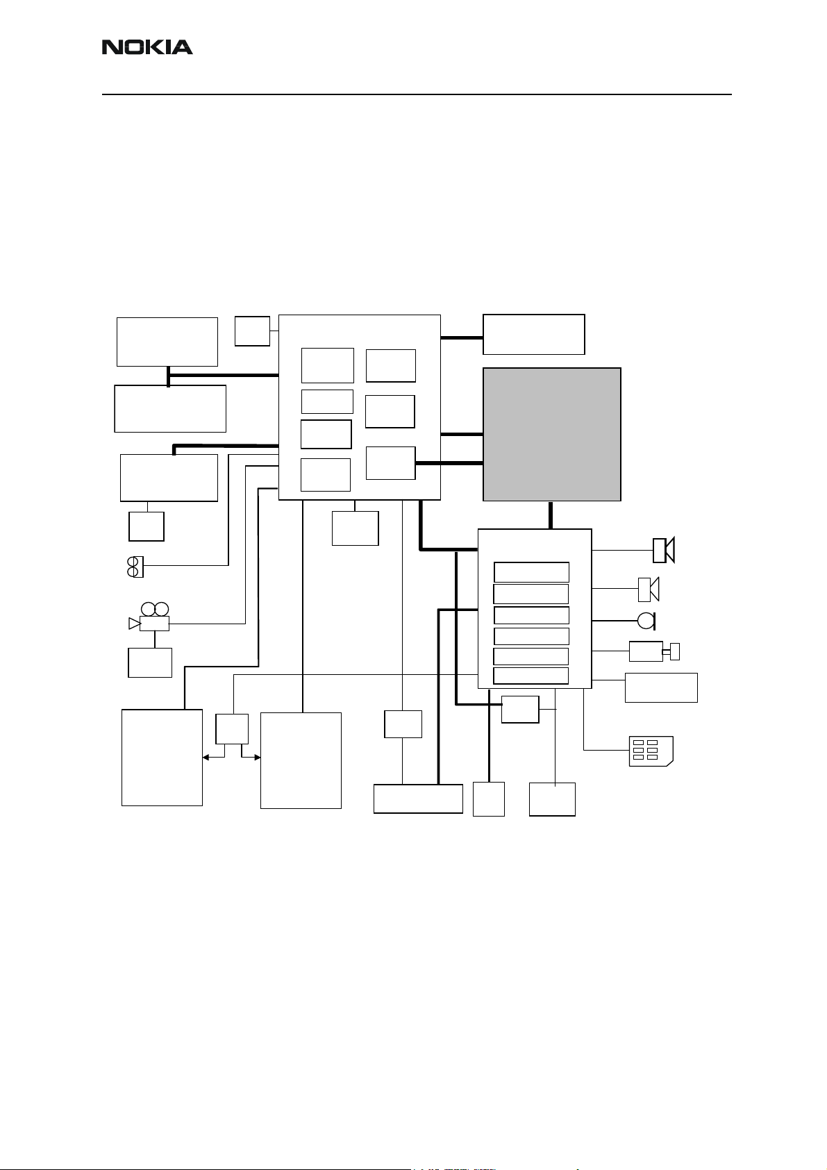
System Module: Baseband
Main functionality of the baseband is implemented into two ASICs: TIKU and UEME.
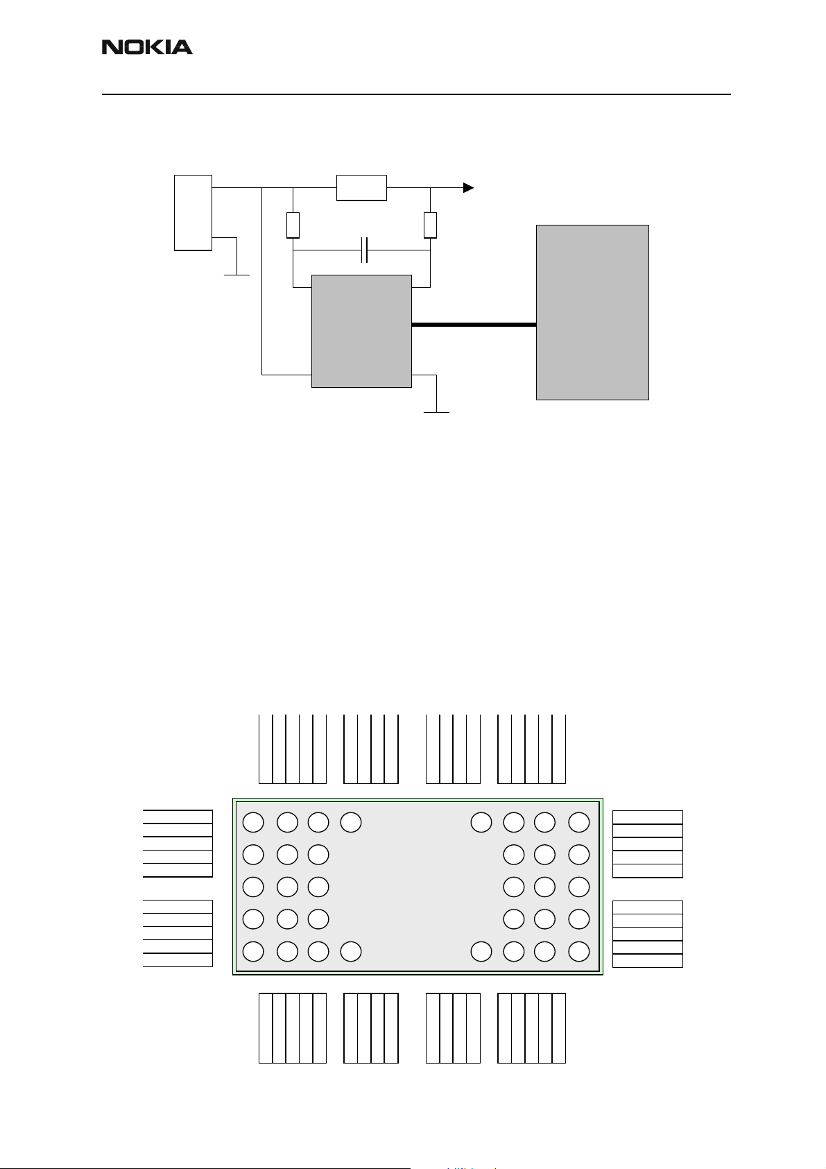
Baseband block diagram:
User data FLASH
256Mbit NAND
FLASH
Program
128Mbit NOR
SDRAM
64Mbit
Core
supply
IR
Camera
supply
Display
Camera
LED
drivers
Core
supply
TIKU
ARM925
PDRAM
CDSP
lead 3
ADSP
lead 3
Keypad
MCU
COWIS
Supply
3G
Logic
2G
Logic
COWIS
NUT
BLUETOOTH
RF Block
UEME
Regulation
Charge control
Audio
FBUS/MBUS
SIM I/F
RTC
Zocus
speaker
Earpiece
MIC
Vibra
Production test
interface
IHF
USIM
Pop-port system
connector
DC
jack
Battery
UEME is the Universal Energy Management Enhanced IC for digital hand portable
phones. In addition to energy management, functionality UEME performs all the baseband mixed–signal functions.
TIKU is the main digital baseband ASIC.
UEME is essentially the same as UEM, but with the following additions:
• An internal IHF amplifier saving the need for an external amplifier and the many
associated passives.
Issue 1 (11/2003) Copyright 2003 Nokia Corporation Page 7-5
Company Confidential
Page 6

NMM-3 Company Confidential
7 - System Module & UI CCS Technical Documentation
• An extra regulator for Tomahawk so saving small area and cost needed for an
external regulator.
• Stereo audio support for stereo tomahawk accessories, which is necessary for the
Music Player.
• Wider audio bandwidth that can be used to improve audio quality of MP3/AAC
and ring tones.
Baseband power is supplied from a 2.8V analogue voltage and 1.8V I/O voltage. UEME
includes 8 linear LDO (Low Drop-Out) regulators for Baseband and 7 regulators for RF. It
also contains 4 current sources for biasing purposes, two for internal use. UEME also
includes a SIM interface, which supports 1.8V and 3V SIM cards. Note: 5V SIM cards are
no longer supported by DCT-4 generation Baseband.
A real time clock function is integrated into UEME, which utilizes the same 32KHz clock
supply as the sleep clock. A backup power supply is provided for the RTC-battery, which
keeps the real time clock running when the main battery is removed. A 10µAh capacitor
provides RTC backup for 3 hours minimum.
The TIKU Brain consists of 5 sections: - the ARM925 Mega-Module, (consisting of the
ARM9 MCU, Cache memory, Parallel LCD Controller, and Traffic Controller), C-DSP Lead 3
Mega-Module, D-DSP Lead 3 Mega-Module, PDRAM, and PDA Peripherals.
The ARM-Mega-Module has a Traffic controller, which provides the interface between
the MCU, external memories, LCD controller, and internal busses. It also processes the
data packages for burst mode memory access.
The PDA Peripherals consists of Camera Compact Port (CCP) interface, IR, USB, and Display interfaces.
The DPLL frequencies are currently:
• MCU: 124.8MHz
• DSPs: 148.0MHz
• PDA: 48MHz
NMM-3 will use TIKU version 1.23
NMM-3 uses a discrete LM2608-1.3 SMPS 1.5V/1.3V regulator for TIKU core supply.
The UEME ASIC handles part of the interface between the baseband and the RF section.
The GSM RX path goes via ADCs in UEME intended for the purpose, but the GSM TX path
uses the dual purpose DACs on board the Tiku baseband ASIC. Tiku DACs are used for
both GSM and WCDMA TX paths. The WCDMA RX path is via Tiku ADCs. UEME also provides the RF section with a DAC for AFC control, a simple "Is RF present?" level detector
TXPWRDET, a DAC for TXC WCDMA power control, two reference voltages VREF01 and
VREF02, and a 4-bit controlled current output IPA1 used for WCDMA PA bias control.
IPA2 is not used. UEME is controlled by Tiku using two serial buses CBUS and DBUS.
CBUS mostly carries commands from the MCU and DBUS mostly carries commands from
the DSP. UEME also contains the analogue parts of the audio codecs which are capable
Page 7-6 Copyright 2003 Nokia Corporation Issue 1 (11/2003)
Company Confidential
Page 7
Company Confidential NMM-3
d
d
N
L
N
Vovp
N
g
CCS Technical Documentation 7 - System Module & UI
of working in various modes from ordinary telephone voice quality to near CD quality. An
8ohm output loudspeaker driver is available for integrated handsfree use. UEME has twin
stereo codecs for stereo headsets. The audio signals are passed from Tiku in the form of
LEFT and RIGHT PDM signals plus and audio clock. The clock and PDM speed changes
according to the quality mode. UEME digital i/o voltages are 1.8V though some of the
internal logic is 2.78V. 2.78V is used for the analogue parts and VBAT is also used for
some of the driver circuits like the vibra, IHF PA, and LED driver.
The Baseband supports both internal and external microphone inputs and speaker outputs. Input and output source selection and gain control is performed by UEME according to control messages from TIKU. Keypad tones, DTMF, and other AUDIO tones are
generated and encoded by TIKU and transmitted to UEME for decoding. An external vibra
alert control signal is generated by UEME with separate PWM outputs.
NMM-3 has two external serial control interfaces: FBUS and USB. FBUS can be accessed
via the test pads, and USB via the system connector.
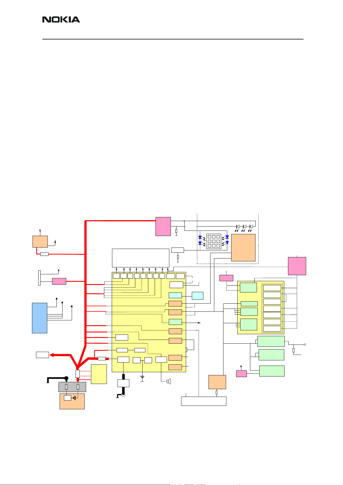
Power Distribution Diagram
The NMM-3 power distribution block diagram is shown below
VIO
Vlogic
IR
Camera
Connector
RF PAs
VFLASH1
Vcc
4R7
UEME VCORE
1.8V
2.8V
LP3985-2.8
2.8 V
VFLASH1
VBAT
20mR
Prot cct
VIO
3.3mR
Battery
contacts
BL-5C
0.22R
ZOCUS
Sense-
Sense+
Vcc
20mR
VREG
VCC
VCC
VCC
VAPP
GND
Vanode
Bluetooth
MANGO GSM/WCDM A RF
BLOCK
VR5
VR4
VR3
VR2
VR1B
VR1A
4.75
4.75
VBATVR1
VBATVR2
VBATVR3
VBATVR4
VBATVR5
VBATVR6
VBATVR7
VBATBB2
VBATBB4
VBATBB5
VBATBB3
VBATBB1
Vibra driver
VBATREGS
V refs Charcon
Charger
Switch
UEME Vchar
protection
Charger
GND
2.8
Jack
2.8
2.8
UEME
VRTC VBU
Back Up
2.8
battery
VR6
2.8
Vin
TK1185
VR7
Audio PA
Vana
Camera
digital supply
UI MODULE
LP2985-1.8
VIO
NUT
(USB IF)
Vcc
33R
VBUS VOUT
Colour LCD
Vcc
Vi/o
Vbat
Vbat
LP3987
2.85V
COWIS
TX/RX
converters
TIK
Clock slicer
I/O
Memory
interface
i/o
VddDi
Core
DPLLs
Periferals
2GBody
ARM9
LEAD3
LEAD3
Voodoo
128Mb NOR Flash
Vcc
Vccq
256Mb NAND
Vcc
Flash
Vccq
64Mb SDRAM
Vccq
Vcc
1.8V
RX
TX
Vbat
LM2608-1.3
DC-DC buck
Vref
1.5V, active
1.3V deep sleep
VTiku
Vpp
12V VPP
gen i/o
+VLCDLED
vfb
VREF01
2.8
-VLCDLED
+VKEYLED
-VKEYLED
KEY LED
Current sink
VREF02
1.35
1.35
GSM RF
converters
VSIM
3.0/1.8V
VFLASH1
2.78V
VIO
1.8V
Vcore
1.8V
VAUX2
2.78V
VANA
2.78V
VAUX1
2.78V
VAUX3
2.78V
IHF
bias
Vdd28
Vdd18
RxAVd
TxAVd
/C
/C
/C
VCHAR
TOMAHAWK (“POP PORT”)
Vcc
SIM
Issue 1 (11/2003) Copyright 2003 Nokia Corporation Page 7-7
Company Confidential
Page 8

NMM-3 Company Confidential
7 - System Module & UI CCS Technical Documentation
Environmental operating conditions
Temperature Conditions:
NMM-3 should operate with full functionality within an ambient temperature range of -
10°C to +60°C, and with reduced functionality between -25°C to -10°C and +55°C to
+75°C.
Humidity and Water Resistance:
Full functionality within humidity range of 5% to 95%.
Condensed or dripping water may cause intermittent malfunctions. Protection against
dripping water has been implemented.
Baseband Functional Description
Modes of Operation
TB4 baseband engine has six different operating modes:
• No supply
• Backup
•Acting Dead
•Active
• Sleep
• Charging
No supply
In NO_SUPPLY mode the phone has no supply voltage. This mode is due to disconnection
of main battery and backup battery or low battery voltage level in both of the batteries.
The phone exits from NO_SUPPLY mode when sufficient battery voltage level is detected.
Battery voltage can rise either by connecting a new battery with VBAT > V
by connecting charger and charging the battery above V
Backup
In BACKUP mode the backup battery has sufficient charge but the main battery can be
disconnected or empty (VBAT < V
and VBACK > 2.0V).
MSTR
MSTR+
.
MSTR+
(2.1V) or
Real Time Clock (VRTC) regulator is disabled in BACKUP mode. VRTC output is supplied
without regulation from backup battery (VBACK). All the other regulators are disabled.
Acting Dead
If the phone is off when the charger is connected, the phone is powered on but enters a
state called ”Acting Dead”. To the user the phone acts as if it was switched off. A battery
charging alert is given and/or a battery charging indication on the display is shown to
acknowledge the user that the battery is being charged.
Page 7-8 Copyright 2003 Nokia Corporation Issue 1 (11/2003)
Company Confidential
Page 9

Company Confidential NMM-3
CCS Technical Documentation 7 - System Module & UI
Active
In the active mode the phone is in normal operation, scanning for channels, listening to
a base station, transmitting and processing information. There are several sub–states in
the active mode depending on if the phone is in burst reception, burst transmission, if
DSP is working etc.
One of the sub–state of the active mode is Bluetooth on state, enabled by UEME. Blutooth circuitry is controlled by the MCU and 26MHz reference clock is generated by the
Module TCXO.
In active mode the RF regulators are controlled by SW writing into UEMEs register settings: VR1A can be enabled or disabled. VR2 can be enabled or disabled and VR4 –VR7
can be enabled or disabled or forced into low quiescent current mode. VR3 is always
enabled in active mode.
Sleep mode
Sleep mode is entered when the MCU and both DSPs are in stand–by mode. Sleep is controlled by the processor. When SLEEPX low signal is detected UEME enters SLEEP mode.
VCORE, VIO and VFLASH1 regulators are put into low quiescent current mode. All RF regulators are disabled in SLEEP. When SLEEPX=1 goes high, UEME enters ACTIVE mode and
all functions are activated.
Battery
The sleep mode is exited either by the expiration of a sleep clock counter in the UEME or
by some external interrupt, generated by a charger connection, key press, headset connection etc.
In sleep mode the 19.2MHz ref clock (VCTCXO) is shut down and 32 kHz sleep clock
oscillator is used as reference clock for the baseband.
Charging
The battery voltage, temperature, size and current are measured by UEME controlled by
the charging software running in TIKU.
The charging control circuitry (CHACON) inside the UEME controls the charging current
delivered from the charger to the battery. The battery voltage rise is limited by turning
the UEME switch off when the battery voltage has reached 4.2 V. Charging current is
monitored by measuring the voltage drop across a 220 mOhm resistor R200.
850 mAh Li-ion battery pack BL-5C is used in NMM-3.
Nominal discharge cut–off voltage 3.35V
Nominal battery voltage 3.7V
Nominal charging voltage 4.2V
Issue 1 (11/2003) Copyright 2003 Nokia Corporation Page 7-9
Company Confidential
Page 10
NMM-3 Company Confidential
7 - System Module & UI CCS Technical Documentation
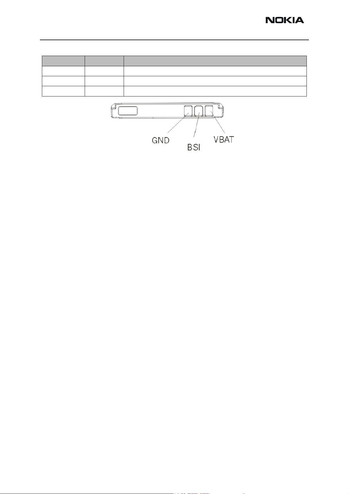
Signal Name Pin Number Function
VBAT 1 Positive battery terminal
BSI 2 Battery capacity measurement (fixed resistor inside the battery pack)
GND 3 Negative/common battery terminal
Battery temperature measurement
In Lynx batteries there are neither BTEMP pin nor NTC resistor. Battery’s temperature is
estimated by the measurement of a discrete NTC resistor in the phone located close to
the battery.
Backup Battery
To preserve the Real Time Clock (RTC), when the main battery is removed, a RTC back-up
capacitor B253 is installed in the phone. This 10uAh solution will give about 3hrs backup time in worst case.
The backup battery (capacitor) is connected between UEME VBACK and GND. In UEME
backup battery charging high limit is set to 3.2V. The cut–off limit voltage (VBUCoff–) for
backup battery is 2.0V. Backup battery
Charging is controlled by MCU by writing to UEME registers.
Power Up and Reset
Power up and reset is controlled by the UEME ASIC. NMM-3 baseband can be powered
up in following ways:
• Press power button which means grounding the PWRONX pin of the UEME
• Connect the charger to the charger input
• Supply battery voltage to the battery pin
• RTC Alarm, the RTC has been programmed to give an alarm
After receiving one of the above signals, the UEME counts a 20ms delay and then enters
it’s reset mode. The watchdog starts up, and if the battery voltage is greater than V
(2.1V) a 200ms delay is started to allow references etc. to settle. After this delay elapses
the VFLASH1 regulator is enabled. 500us later VR3, VANA, VIO and VCORE are enabled.
Finally the PURX (Power Up Reset) line is held low for 20 ms. this reset, PURX, is fed to
the baseband ASIC TIKU, resets are generated for the MCU and DSPs. During this reset
phase the UEME forces the VCTCXO regulator on regardless of the status of the sleep
control input signal to the UEME.
coff+
Page 7-10 Copyright 2003 Nokia Corporation Issue 1 (11/2003)
Company Confidential
Page 11
Company Confidential NMM-3
U
CCS Technical Documentation 7 - System Module & UI
All baseband regulators are switched on at the UEME power on except SIM and VAUX1,
2, 3 regulators that are controlled by the MCU (VFLASH2 is not used on NMM-3). The
UEME internal watchdogs are running during the UEME reset state, with the longest
watchdog time selected. If the watchdog expires the UEME returns to power off state.
The UEME watchdogs are internally acknowledged at the rising edge of the PURX signal
in order to always give the same watchdog response time to the MCU.
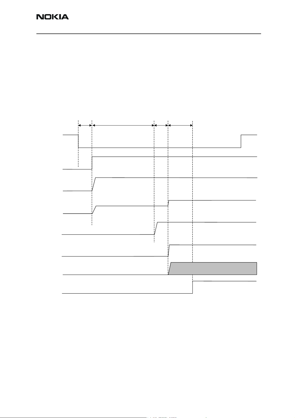
UEME Reset Sequence and Timings
The diagram below shows the timing of the reset sequence on the NMM-3.
POWERONX
EMRSTX
VRAM (SDRAM core)
VTIKU (Tiku core)
VFLASH1
VIO, VR3, VANA,
SMPSCLK
Delay1
20ms
Delay2
200ms
1.3V
Delay3
0.5ms
Delay4
20ms
1.5V
RFCLK
(19.2MHz)
PURX, SLEEPX
A/D Channels
The UEME contains the following A/D converter channels that are used for several measurement purpose. The general slow A/D converter is a 10-bit converter using the UEME
interface clock for the conversion. An interrupt will be given at the end of the measurement.
The UEME’s 13–channel analog to digital converter is used to monitor charging functions, battery functions, voltage levels in external accessory detection inputs, user interface and RF functions.
Issue 1 (11/2003) Copyright 2003 Nokia Corporation Page 7-11
Company Confidential
Page 12

NMM-3 Company Confidential
7 - System Module & UI CCS Technical Documentation
The monitored battery functions are:
• Battery voltage (VBATADC),
• Battery type (BSI)
• Battery temperature (BTEMP).
The battery type is recognized through a resistive voltage divider. In phone there is a
100kOhm pull up resistor to VFLASH1 in the BSI line and the battery has a pull down
resistor in the same line. Depending on the battery type the pull down resistor value is
changed. The battery temperature is measured equivalently except that the NTC pull
down resistor used for temperature sensing is on the phone.
The monitored charger functions are:
• Charger Voltage (VCHAR)
• Charger current (ICHAR)
The voltage measured across a 0R22 resistor (R200) in circuit with charger voltage out
from UEME is used to determine ICHAR.
ZOCUS
The HEADINT and HOOKINT are external accessory detection inputs used for monitoring
voltage levels in these inputs. They are routed internally from the miscellaneous.
The monitored RF functions are:
• Power amplifier temperature (GRFTEMP)
• VCXO Temperature (WTx_TEMP)
PATEMP input is used to measure temperature of the TEX and HLGA.
A/D values can be monitored through the ‘ADC Reading’ window in Phoenix.
The ZOCUS device N201 (National LM3819) is a calibrated current sensor, used by energy
management software to determine the current consumption in the mobile phone.
Current is sensed across a “zero-ohm” PWB track resistor (actual trace resistance is
~3.3mΩ) using a high gain and extremely low offset comparator. The measured current
is converted to a pulse width modulation (PWM) signal with the duty cycle representing
both the magnitude and direction of current. The PWM signal is converted to digital data
that can be read by the phone via the CBUS interface.
ZOCUS reads the average current over a period of approximately 1 second.
Page 7-12 Copyright 2003 Nokia Corporation Issue 1 (11/2003)
Company Confidential
Page 13
Company Confidential NMM-3
CCS Technical Documentation 7 - System Module & UI
To determine the functionality of ZOCUS, use Phoenix ADC Reading option to read the
phones Battery average current, the value returned is calculated from values measured
by ZOCUS. Also self-test will prove CBUS connectivity to ZOCUS.
Bluetooth
VBAT
BSI
GND
Current Sense
track resistor
VBAT
UEME
Sense In
ZOCUS
N201
VDD GND
CBUS
D200
The Bluetooth circuit consists of the Bluetooth module (N101), A TCXO (G100) operating
at 26MHz.
The BT202 Bluetooth transceiver module for NMM-3, consists of a RF ASIC, Baseband
ASIC and 4Mbits Flash Memory. It contains UART and PCM user interface. The supply
voltage is VBAT, VFLASH1 and VIO. External reference clock is 26 MHz.
The Bluetooth module is not a repairable part, and so should be replaced if found to be
defective..
56:XTALGND
55:XTAL
54:VCC
53:VCC
52:VCC
51:GND
50:SYSCLK
49:VBB EN
1:GND
2:GND
3:GND
4:GND
5:GND
6:VRE G
7:GND
8:GND
9:GND
10:GND
48:SLEEP X
xxxxxxx
xxxxxxxxxxxxx
47:GND
46:VCC XTAL
45:VDD
44:RESETX
43:GPP2
42:WRX
41:GPP3.
40:GPP4
39:GND
38:GPP0
37:GPP1
36:GPP10
35:GPP11
34:CENX
33:GND
32:VAPPL
31:OSCON
30:GPP9
29:GND
11:G ND
12:ANT
13:GND
14:GND
15:GND
16:REFCLK
17:GND
18:EN26MH Z
19:GND
20:TRST
21:TMS
22:TDO
23:TDI
24:GPP5
25:TCK
26:SPLCLK
27:GPP7
28:GPP6
Issue 1 (11/2003) Copyright 2003 Nokia Corporation Page 7-13
Company Confidential
Page 14
NMM-3 Company Confidential
7 - System Module & UI CCS Technical Documentation
Pin Description:
No.
44 RESETX PURX BB reset input from UEME
50 SYSCLK1 SYSCLK system clock_input / 26MHz from TCXO G100
55 XTAL - internal 13MHz oscillator / Not connected
56 XTALGND GND Select oscillator / Ground
18 EN26MHZ VIO Defines system clock / connected to VIO for 26MHz
16 REFCLK GND Reference clock input / connected to Ground
26 SLPCLK SLEEPCLK Sleep clock input from UEME
49 VBBEN UEMRSTX Internal RF regulators enabled by UEME ResetX
48 SLEEPX SLEEPX Switch to active mode
31 OSCON OSCON Force active mode(=ResetX for Flash)
1-5, 7-11, 13-
15, 17,19,
29,33,
39,47,51
52-54 VCC VBAT_BT Main power supply voltage input from Battery
6 VREG VFLASH1 Regulated power supply voltage input 2.78V from
46 VCCXTAL VCCXTAL Regulated 2.4V supply output for external TCXO G100
Bluetooth
Name
GND GND Ground reference
NMM-3 Name Function / Destination
VFLASH1, used for RF and BB parts.
45 VDD GPP3 Regulated 1.8V supply for internal BB and Memory
Blocks
32 VAPPL VIO 1.8V supply for application interfacing
12 ANT ANT Antenna pin
38 GPP0 LPRFSYNC General purpose port / Data Bus
37 GPP1 LPRFINT Interrupt to TIKU to initilise BT operation.
43 GPP2 GND General purpose port connected to Ground
41 GPP3 VDD General purpose port supply for internal BB and Mem-
ory Blocks
40 GPP4 - General purpose port / No Connection
24 GPP5 GND General purpose port connected to Ground
28 GPP6 LPRFRX General purpose port / Data Bus
27 GPP7 LPRFTX General purpose port / Data Bus
30 GPP9 - General purpose port / No Connection
36 GPP10 CBUSCLK General purpose port used for control and flash pro-
gramming
35 GPP11 CBUSDA General purpose port used for control and flash pro-
gramming
34 CENX CBUSENX CBUS enable / No Connection
20 TRST - JTAG test reset / No Connection
21 TMS - JTAG test mode / No Connection
Page 7-14 Copyright 2003 Nokia Corporation Issue 1 (11/2003)
Company Confidential
Page 15

Company Confidential NMM-3
CCS Technical Documentation 7 - System Module & UI
Camera
No.
22 TDO - JTAG test output / No Connection
23 TDI - JTAG data input / No Connection
25 TCK - JTAG clock / No Connection
42 WRX - Write enable / No Connection
Bluetooth
Name
NMM-3 Name Function / Destination
A 14-way connector connects the camera and shield housing attached is on B-side of
the engine. This uses the differential camera interface on TIKU.
1.8V Supply: UEME VCORE programmed to 1.8V at start-up.
Camera 2.7V supply:
LP3985-2.8 discrete regulator N102 controlled by GPIO7 is used for analogue supply.
Output 1 = ON.
Both camera supplies are enabled /disabled as the camera activity is required.
The camera switch is a discrete button connected to TIKU GPIO6.
The Camera / TIKU interface comprises of two synchronous serial Buses:
• IIC Bus for control
• Fast differential Camera Interface for image data out
Camera
No.
Name
1 GND1 GND GPIO7 TIKU Ground line corresponding to VDDI
2 SDA CAMSDA GENIO26 TIKU Serial data line of IIC bus
3 D+ CIFDAP CIFDaP TIKU Fast serial data out
4 SCL CAMSCI GENIO25 TIKU Serial clock line of IIC bus
5 D- CIFDAN CIFDaN TIKU Fast serial data out of which phase is inverted to D+
6 Extclk CAMCLK GENIO24 TIKU System clock from engine to the camera
7 VDDI VCORE VCORE UEME 1.8V Supply voltage to a camera module (for digital)
8 GND3 GND GND Ground line corresponding to Extclk.
9 CLK + CIFCLKP CIFClkP TIKU Fast serial clock
NMM-3
Name
NMM-3 Destination Function
module.
10 Vctrl CAMVCTRLGENIO27 TIKU This signal is used for activating the camera
module When Vctrl is turned “High”, the
camera module enters the operation mode.
When Vctrl is turned “Low”, the camera
module enters the power off mode.
Issue 1 (11/2003) Copyright 2003 Nokia Corporation Page 7-15
Company Confidential
Page 16

NMM-3 Company Confidential
7 - System Module & UI CCS Technical Documentation
Camera
No.
Name
11 CLK - CIFCLKN CIFClkN TIKU Fast serial data out which is inverted to Clk+
12 VDD VCAM VOUT N102 Reg 2.8V Analog supply Voltage
13,14 GND2 GND GND Ground line corresponding to VDD
NMM-3
Name
NMM-3 Destination Function
UI Module
The UI Module comprises of:
•LCD Display
• Display and Keypad Backlight LED’s
• Light Guide
•Key Domes
• Engine Shielding
Display
NMM-3 uses a Sharp active matrix LCD (Liquid Crystal Display) module. The module is
comprised of a glass panel, driving IC’s, a backlight system with three white LED’s (LightEmitting Diode’s), and a metal frame. The display panel performs RGB with 132 × 162
dot resolution.
For details on signal connections, see ‘UI Module Pin Description’ table below.
Backlighting
NMM-3 UI module has 2 sets of LEDs:
To enable flexibility in driver solution, the engine/UI interface has been arranged with
the power supplies separate. i.e. paired supplies +VLCDLED,-VLCDLED, and +KEYLED, KEYLED
Power is supplied by a Toko LED driver.
In block form the LED driver arrangement is shown below.
The TOKO boost supply switches at 600kHz 18V max. LCDLED current set by 22R resistor
across the TOKO 0.5V reference voltage
The constant current sink used for the KeyLEDs is used for tight current control but
allowing the widest possible VF (Forward Voltage) tolerance for the KEYLEDs.
• 3off LCD LEDS: Nichia NSCW215T WHITE. Wired in series. Required current = 22mA.
• 4off KEY LEDS: Citizen CL270B blue Wired in two series chains of 2. Current ~ 8.5mA.
Page 7-16 Copyright 2003 Nokia Corporation Issue 1 (11/2003)
Company Confidential
Page 17

Company Confidential NMM-3
CCS Technical Documentation 7 - System Module & UI
DLIGHTPWM
VFLASH1
VBAT
TOKO 350mA pk
boost circuit.
Switching
freq=600kHz
10.5V nom
0.5V
33R
22R
+KEYLED
+LCDLED
-LCDLED
10mA max
15mA
22mA
White
LCD
LEDS
Blue
KEY
LEDS
KLIGHTPWM
constant current sink
(8.5mA)
1.9V
220R
3.5V
-KEYLED
ENGINE
MODULE
UI
MODULE
LED brightness is controlled by a PLUM to DLIGHT and KLIGHT enable. In order to improve
the LED’s lifetime, the brightness is reduced at high levels of ambient temperature.
UI Module Pin Description:
UI Connector LCD Connector Function
PIN Name PIN Name
1 VFLASH1 10 VFLASH1 Power supply for analog display circuits (2.8V)
2 - 9 PSD Not Connected
3 -VLCDLED 1 VLED- LCD LED power supply (cathode)
4 +VLCDLED 2 VLED+ LCD LED power supply (anode)
5 VIO 3 VDDI Power supply for digital display circuits (1.8V)
6 DIFD7 4 D7 Display Bi-directional Bus (MSB)
7 COL0 Keypad Column
8 ROW5 Keypad Row
9 GND Ground
10 GND Ground
11 COL1 Keypad Column
12 DIFD6 5 D6 Display Bi-directional Bus
13 DIFD5 6 D5 Display Bi-directional Bus
14 DIFD4 7 D4 Display Bi-directional Bus
15 DIFD3 8 D3 Display Bi-directional Bus
16 +VLCDLED Key Backlighting +Ve
17 EARN Earpiece -Ve
18 EARP Earpiece +Ve
19 -VLCDLED Key Backlighting –Ve
20 DIFD2 13 D2 Display Bi-directional Bus
21 DIFD1 14 D1 Display Bi-directional Bus
22 DIFD0 15 D0 Display Bi-directional Bus (LSB)
23 DIFA0 16 A0 Command (A0 = low) or parameter (A0 = high)
Issue 1 (11/2003) Copyright 2003 Nokia Corporation Page 7-17
Company Confidential
Page 18

NMM-3 Company Confidential
7 - System Module & UI CCS Technical Documentation
UI Connector LCD Connector Function
PIN Name PIN Name
24 COL2 Keypad Column
25 ROW4 Keypad Row
26 ROW3 Keypad Row
27 GND 11 GND Ground
28 GND 12 GND Ground
29 ROW2 Keypad Row
30 ROW1 Keypad Row
31 ROW0 Keypad Row
32 COL3 Keypad Column
33 DIFRDX 17 RDX Memory read enable (active low)
34 DIFWRX 18 WRX Memory write enable (active low)
35 LCDRSTX 20 RESX Reset (active low)
36 GND 19 GND Ground
IR Module
As there are no level shifters in UEME, a 1.8V logic interface 1M IR. compliant module
from Citizen: CIM-93M5 is used. It is a shielded package to reduced EMC susceptibility
to GSM/WCDMA emissions.
The IR link supports speeds from 9600 bit/s to 1.152 MBit/s up to distance of 1m. Transmission over the IR is half–duplex.
The length of the transmitted IR pulse depends on the speed of the transmission.
At speeds of 115.2 kbit/s or less (SIR), pulse lengths are kept close to the minimum of
1.41us specified by IrDA in order to keep current consumption to a minimum. If transmission speed is set to 1.152Mbit/s (MIR) the pulse length is approximately150ns. Signal
rates of 0.576Mbits/s and greater than 1.152 MBit/s are not supported by NMM-3.
IR Module Pin Description:
PIN Name Function Active
1 LEDA LED Anode -
2 LEDC LED Cathode: No connection -
3 TXD Transmitter Data Input High
4 RXD Received Data Output Low
5 SD Shut Down High
6 Vcc Supply Voltage (VFLASH1) -
7 Vlogic Digital Supply Defining I/O Voltage (VIO) -
8 GND Ground -
Shield EMI Shield (Ground)
Page 7-18 Copyright 2003 Nokia Corporation Issue 1 (11/2003)
Company Confidential
Page 19

Company Confidential NMM-3
CCS Technical Documentation 7 - System Module & UI
SIM Interface
NMM-3’s SIM interface uses the standard DCT4 interface, provided by TIKU and UEME.
This complies with international standard specifications.
The SIM interface signals are protected by SIM EMC/ESD ASIP (R407).
UEME contains the SIM interface logic level shifting. SIM interface can be programmed
to support 3V and 1.8V SIMs. SIM supply voltage is selected by a register in the UEME. It
is only allowed to change the SIM supply voltage when the SIM IF is powered down. The
SIM power up/down sequence is generated in the UEME. This means that the UEME generates the RST signal to the SIM. Also the SIMCardDet signal is connected to UEME. The
card detection is taken from the BSI signal, which detects the removal of the battery. The
monitoring of the BSI signal is done by a comparator within UEME. The comparator offset is such that the comparator output does not alter state as long as the battery is connected. The threshold voltage is calculated from the battery size
specification. The SIM interface is powered up when the SIMCardDet signal indicates
‘card in’. This signal is derived from the BSI signal.
Parameter Min Typ Max Unit
SIMCARDET, BSI comparator threshold 1.94 2.1 2.26 V
SIMCARDET, BSI comparator hysteresis 50 75 100 mV
The whole SIM interface locates in TIKU and UEME. The SIM interface in the UEME contains power up/down, port gating, card detect, data receiving, ATR–counter, registers and
level shifting buffers logic. The SIM interface is the electrical interface between the Subscriber Identity Module Card (SIM Card) and mobile phone (via UEME device).
Issue 1 (11/2003) Copyright 2003 Nokia Corporation Page 7-19
Company Confidential
Page 20

NMM-3 Company Confidential
7 - System Module & UI CCS Technical Documentation
External Accessory Interface
Pop-Port System Connector
Because of NMM-3’s shape, there is one deviation from the Tomahawk (pop-Port)
mechanical interface that affects an in-car holder solution: The charger jack will be
mounted remotely from the system connector.
The charger pin on the Pop-Port interface is not connected. This prevents a possible connection between charging accessories, and chargers connected into a separate DC charging jack. Pop-Port chargers are not supported.
Pin No / Signal
Name
1. Charge V Charge DC 0-9V / 0.85A Not connected on NMM-3
2. GND Charge GND - 0.85A
3. ACI ACI 1 kbit/s Digital 0 / 2.5V – 2.78V Accessory insertion and
4. Vout DC out DC 2.78V 70mA
5. USB Vbus DC in DC 4.375V – 5.25V
6. USB D+ / FBUS Rx USB 12M USB 0V – 3.3V FBUS not connected on Mango
7. USB D- / FBUS Tx USB 12M USB 0V – 3.3V FBUS not connected on Mango
8. USB data GND Data GND -
9. XMIC N Audio in 300 – 8k 1 Vpp & 2.5V – 2.78V DC
10. XMIC P Audio in 300 – 8k 1 Vpp & 2.5V – 2.78V DC
11. HSEAR N Audio out 20 – 20k 1 Vpp
12. HSEAR P Audio out 20 – 20k 1 Vpp
13 HSEAR R N Audio out 20 – 20k 1 Vpp
14. HSEAR R P Audio out 20 – 20k 1 Vpp
Signal
Description
Spectral
Range
Voltage / Current Levels Notes
removal detect
70mA
2.50V 90mA
Page 7-20 Copyright 2003 Nokia Corporation Issue 1 (11/2003)
Company Confidential
Page 21

Company Confidential NMM-3
CCS Technical Documentation 7 - System Module & UI
A B
Charger connector
Pin No / Signal
Name
Signal
Description
Spectral
Range
Voltage /
Current Levels
A. GND Charge GND - 0.85A
B. Charge V Charge DC 0-9V / 0.85A Inner pin
Charger interface.
NMM-3 conforms to the global Nokia Charger Interface
ACI
The ACI (Accessory Control Interface) is a point-to-point, bi-directional serial bus. It has
two main features:
• The insertion and removal detection of an accessory device.
• Acting as a data bus between phone and accessory, Intended for control purposes.
A third function of ACI is to identify and authenticate the accessory.
Accessory power is supplied by VAUX2, a linear low dropout regulator in UEME providing
2.78V at 70mA maximum when active (0.5mA in sleep).
Notes
ACI data passes to and from UEME via the HEADINT line. UEME level shifts the data and
connects HEADINT to MBUS for TIKU to access.
USB interface
ARM92
TIKU
D300
W2FC
core
USBSEMODE
USBPUEN
USBSUSPEND
USBVP/FRX
USBVM
USBRCV
USBV0
USBFSE0
USBOEX
VIO
NUT
N401
VBUS
VPU
D-
D+
33R
USB ASIP
R409
33R
33R
1k5
Tomahawk
Connector
VBUS
D-
D+
Issue 1 (11/2003) Copyright 2003 Nokia Corporation Page 7-21
Company Confidential
Page 22

NMM-3 Company Confidential
7 - System Module & UI CCS Technical Documentation
The Nokia USB device solution is supported using the Wireless 2 Function Controller
(W2FC) core block in the TIKU ASIC. The core completes several USB functions automatically and is controlled by the ARM9 MCU.
NUT (D300)provides the interface between the ASIC's 1.8 V bus and the 3.3 V USB data
bus.
Nokia USB Transceiver (NUT) is fully compliant with the Universal Serial Bus Specification Rev. 1.1.
NUT is able to transmit and receive serial data at both full-speed. In NMM-3, its lowspeed (1.5 Mbit/s) capability is only used in SE (single ended) mode in production loopback test. FBUS is not supported on NMM-3
External Audio
The NMM-3 is designed to support fully differential external accessories connecting via
the Pop-Port system connector. Features supported are:
• 4-Wire fully differential stereo audio output.
• 2-Wire differential mic input.
• ACI for detection and data interface.
External Microphone Connection
The external microphone input is fully differential lines are connected to UEME microphone inputs MIC2N and MIC2P. The UEME (MICB2) provides the bias voltage. Microphone input lines are ESD protected.
A short circuit between the headset microphone signals generates a HOOKINT signal.
When the accessory is not connected, a pull-up resistor internal to UEME holds the
HOOKINT line to VFLASH1 (2.8V). When the accessory is connected the voltage on
HOOKINT drops to 1.8V due to the bias current flowing through the 1KΩ ASIP resistors
R415. When the button is pressed the microphone signals are connected together, and
the HOOKINT input will get half of the mic bias DC value 1.1V. This change in the DC
level will cause the HOOKINT comparator to change state, in this case from 0 to 1. The
button can be used for answering in coming calls, but not to initiate outgoing calls.
Page 7-22 Copyright 2003 Nokia Corporation Issue 1 (11/2003)
Company Confidential
Page 23

Company Confidential NMM-3
R
CCS Technical Documentation 7 - System Module & UI
External Microphone connection:
HOOKINT
MICB2
UEME
D200
MIC2P
MIC2N
R415
EMC / ESD
Components
XMICP
XMICN
System
Connector
Pop-Port
External Earphone Connections
The external earphone output has stereo fully differential lines are connected to UEME
HF outputs HF, HFCM, HFR and HFCMR.
The external audio is processed by the Audio Receive Path in UEME, and controlled by
TIKU. UEME performs the following functions:
• Digital to analog conversion of EAR DATA, and low pass filtering (common to all
Rx audio)
• Programmable attenuating stage
• Stereo HF and HFCM drivers
External Earphone connections:
HFCM
HF
UEME
D200
HFCMR
HFR
EMC / ESD
Components
XEARN
XEARP
XEARN
XEARP
System Connector
Pop-Port
Internal Audio
IHF Speaker
The Integrated Hands Free Speaker is used to generate speech audio, alerting and warning tones. The speaker capsule is mounted in the C-cover. Spring contacts are used to
connect the IHF speaker to the Engine PWB. The IHF speaker is driven directly from UEME
that incorporates the audio power amplifier and a programmable attenuation stage.
Issue 1 (11/2003) Copyright 2003 Nokia Corporation Page 7-23
Company Confidential
Page 24

NMM-3 Company Confidential
N
7 - System Module & UI CCS Technical Documentation
IHF speaker connections:
UEME
Internal Microphone
The internal microphone capsule is mounted in the C-cover. The microphone is omni
directional and is connected to UEME microphone inputs MIC1P and MIC1N. The microphone input is asymmetric and the UEME (MICB1) provides a bias voltage. The audio
transmit path functional blocks included in UEME are:
• Microphone input stage
• Programmable gain stage
• Anti-aliasing lowpass filter
D200
PAOUTP
PAOUTN
• Analog to digital converter
Spring contacts are used to connect the microphone to the engine PWB.
Internal Microphone connection:
MICB1
UEME
D200
MIC1P
MIC1
Internal Speaker
The internal earpiece is a dynamic earpiece with an impedance of 32Ω. The earpiece is
fitted to the UI module. The earpiece is driven directly by UEME. UEME includes the same
functional blocks as the external earphone, but with a separate earpiece driver. The earpiece output from UEME is ESD protected.
Page 7-24 Copyright 2003 Nokia Corporation Issue 1 (11/2003)
Company Confidential
Page 25

Company Confidential NMM-3
N
CCS Technical Documentation 7 - System Module & UI
UEME
Memory Block
PDRAM
The PDRAM block is the internal memory system for TIKU. It contains the following subblocks:
• Boot ROM, containing MCU program code. The boot ROM size is 4k bytes (1k x
32).
• 256 Kbytes of x32 RAM (organized as 4 banks of 16k x 32) for the Cellular DSP
code.
UI Module
D200
EARP
EAR
• 256 Kbytes of x32 RAM (organized as 3 banks of 16k x 32 and 2 banks of 8k x 32)
for Application DSP code and data, all performance critical code is located here.
• One 4Kbytes (organized as 2k x 16) dual-port RAM, accessible by both Application DSP and Cellular DSP.
External Flash Memory
NMM-3 uses conventional 128Mb “NOR” Flash for the program data and storage of
PMM calibration data, and a 256Mb “NAND” flash for the user data storage (pictures,
music, voice clips, etc).
Program Flash:
4341433 Samsung 128Mb Flash D451
User Flash
434xxxx Samsung 256Mb NAND Flash D450
External SDRAM
4341341 Samsung 64Mb SDRAM is used in NMM-3.
The SDRAM core supply is provided by regulator N450 and is the LP3987-2.85.
SDRAM core control in NMM-3 is as follows:
Issue 1 (11/2003) Copyright 2003 Nokia Corporation Page 7-25
Company Confidential
Page 26

NMM-3 Company Confidential
7 - System Module & UI CCS Technical Documentation
Pin Control System control
enable 1=On UEMRSTX enabled at UEME delay0
0=0ff
mode 1=ON SLEEPX Rises when PURX=1, then under deep sleep control.
NMM-3 Test interfaces
The following interfaces available:
• 9 way test access pads including Fbus, flashing, DAI if needed (Mbus pin) and STI.
• 3-way battery interface repeated under the battery used for production test.
• Service software will use Phoenix SW via USB on Pop-Port connector or FBUS via
the FLA-45 service battery or JBV-1 docking station.
Baseband General Specification
Absolute Maximum Ratings
Signal Limit
Battery Voltage (Idle) -0.3 - +5.5V
Battery Voltage (Call) 4.8V MAX
Charger Input Voltage -0.3V - +16V
DC Characteristics
Regulators and Supply Voltage Ranges
Battery Voltage Range
Signal Min Nom Max
VBAT 3.1V 3.7V 4.2V (Charging high limit target voltage)
BB Regulators
Signal Min Nom Max Output Current
VANA 2.70V 2.78V 2.86V I
VFLASH1 2.70V 2.78V 2.86V I
VAUX2 2.70V 2.78V 2.86V I
VSIM 1.745V
2.91V
VIO 1.72V 1.8V 1.88V I
VCORE 1.71V 1.8V 1.89V I
1.8V
3.0V
1.855V
3.09V
max
max
I
sleep
max
I
sleep
I
max
I
sleep
max
I
sleep
max
= 80mA
= 70mA
= 1.5mA
= 70mA
= 0.5mA
= 25mA
= 0.5mA
= 150mA
= 0.5mA
= 200mA
Page 7-26 Copyright 2003 Nokia Corporation Issue 1 (11/2003)
Company Confidential
Page 27

Company Confidential NMM-3
CCS Technical Documentation 7 - System Module & UI
RF Regulators
Signal Min Nom Max Output Current
VR1A / VR1B 4.60V 4.75V 4.90V I
VR2 2.70V
2.61V
VR3 2.70V 2.78V 2.86V I
VR4 2.70V 2.78V 2.86V I
VR5 2.70V 2.78V 2.86V I
VR6 2.70V 2.78V 2.86V I
VR7 2.70V 2.78V 2.86V I
2.78V
2.78V
2.86V
2.95V
max
I
max
max
max
I
sleep
max
I
sleep
max
I
sleep
max
= 10mA
= 100mA
= 20Ma
= 50mA
= 0.1mA
= 50mA
= 0.1mA
= 50mA
= 0.1mA
= 45mA
Current Sources
Signal Min Nom Max Note
IPA1 and IPA2 0 – 5mA Programmable, +/-6% V
V
= 0V – 2.7V
IPA2
IPA3 and IPA4 95µA 100µA 105µA V
IPA3
/ V
= 0V – 2.7V
IPA4
IPA1
/
RF Module Description
Introduction
This document describes the RF module of the dual system WCDMA, GSM (EGSM900,
GSM1800) engine for N-MM3. Electrical specifications, functional descriptions and block
diagrams are included. The WCDMA RF is supporting 3GPP rel 99 and GSM RF is supporting GPRS and HSCSD classes 1 to 6.
DC characteristics
Regulators
The RF regulators are found in UEME in the baseband section of the phone. There are six
2.78 V regulators VR2-VR7 and two 4.8V regulators VR1A and VR1B. There is also a
1.35V regulator VrefRF01 which is used as the reference voltage for the RF ICs. Regulators EXT.Reg1 and EXT.Reg2 are external to UEME and are used in the WCDMA Tx section.
Table 1: Voltage supplies and references
Signal name From To Function
VBAT Battery GSM/WCDMA PA SMPS
& UEME
VR1A UEME REX & HELGO VCO control charge pump.
VR1B UEME TEX VCO control charge pump.
Battery supplies.
Issue 1 (11/2003) Copyright 2003 Nokia Corporation Page 7-27
Company Confidential
Page 28

NMM-3 Company Confidential
7 - System Module & UI CCS Technical Documentation
Table 1: Voltage supplies and references
Signal name From To Function
VR2 UEME TEX, HELGO WCDMA: TEX supply voltage
GSM: VRF_TX.
VR3 UEME VCTCXO, HELGO VCTCXO.
GSM: VDIG. RFCLK buffer
VR4 UEME REX, HELGO WCDMA: REX LNA, demod, biasing, local buffer.
GSM: VRF_RX, VF_RX, VBB
VR5 UEME REX, HELGO WCDMA: REX BB gain, filter, AGC, VLO, synthe-
sizer.
GSM: VLO, VPRE
VR6 UEME RX VCO WCDMA: RX VCO
VR7 UEME GSM VCO GSM: VCO
VrefRF01 UEME REX, HELGO, TEX, HEX Voltage Reference for RF ICs 1.15% accuracy.
EXT. Reg 1
EXT. Reg 2
1st discrete
2nd discrete
TX VCO WCDMA: TX VCO
WCDMA TX WCDMA: Supply voltage for HEX, PA Vreg, power
detector
VCTCXO
WCDMA
RX VCO
GSM VCO
UEME
TEX
HEX
REX
VR1A
VR1B
VR2
VR3
VR4
VR5
VR6
EXT REG 2
HEX
WCDMA p wr
det
VBAT
EXT REG 1
WCDMA TX
VCO
GSM PA
PA
SMPS
WCDMA PA
HELGO
VR7
VrefRF
01
WCDMA PA
Figure 1: Voltage supplies for RF
Page 7-28 Copyright 2003 Nokia Corporation Issue 1 (11/2003)
Company Confidential
Page 29

Company Confidential NMM-3
CCS Technical Documentation 7 - System Module & UI
RF-BB Interface
Table 2: Binary signals
Signal name From To Function
RFBusEn1X TIKU RF (REX, TEX, HELGO) Data enable for RF-IC
RFBusDa TIKU RF (REX, TEX, HELGO) Data for PLL and RX AGC
RFBusClk TIKU RF (REX, TEX, HELGO) Clock
RXA1/GenIO 9 TIKU REX WCDMA RX AGC one step tuning
RXA2/GenIO 10 TIKU REX WCDMA RX AGC one step tuning
TXP/GenIO 2 TIKU HELGO GSM transmitter power amplifier enable
REXRstX/GenIO 7 TIKU REX REX reset
TEXRstX/GenIO 1 TIKU TEX TEX reset
HelgoRstX/GenIO 5 TIKU HELGO HELGO reset
TXVCOpwr/GenIO 0 TIKU ExtReg1 WCDMA TX VCO enable
HEXPD/GenIO 8 TIKU HEX HEX power down
TXpwr/GenIO 13 TIKU ExtReg2 WCDMA TX pwr enable
PApwr/GenIO 15 TIKU WCDMA RF PA SMPS WCDMA PA SMPS enable
Table 3: Analog signals
Signal name From To Function
RFCLK HELGO TIKU Reference clock to Baseband
AFC UEME VCTCXO Frequency control signal to VCTCXO
WRXIP/M REX TIKU Differential RX base band signals for main receiver I branch.
WRXQP/M REX TIKU Differential RX base band signals for main receiver Q branch.
TXIP/M TIKU TEX TX I/Q signals to the modulator
TXQP/M TIKU TEX TX I/Q signals to the modulator
GRXI/GRXQ HELGO UEME RX base band signal
TxPwrDet WCDMA_RF UEME TX power envelope detector
TXA1 TIKU TEX TEX AGC control
TXA2 TIKU HEX PA driver AGC control
IPA1 UEM WCDMA_PA PA bias control
Iref1 TEX TIKU Reference current for AD converters
Iref2 TEX TIKU "
CALOUT REX TIKU WCDMA BB filter calibration
VREFCAL TEX TIKU WCDMA BB filter calibration (ref. Voltage)
WTxTemp TEX UEME TEX temp.
VREFL REX TIKU Reference voltage for AD converters
VREFM REX TIKU "
VREFH REX TIKU "
GRFTemp HELGO UEM GSM temp.
Issue 1 (11/2003) Copyright 2003 Nokia Corporation Page 7-29
Company Confidential
Page 30

NMM-3 Company Confidential
7 - System Module & UI CCS Technical Documentation
Table 3: Analog signals
Signal name From To Function
TXC UEME HELGO,
WCDMA PA
SMPS
RF block diagram
General
The GSM and WCDMA RF engines are based on direct conversion architecture.
GSM TX/RX design is based around the HELGO RF ASIC.
The WCDMA RX design is based around the REX ASIC. The WCDMA TX design uses TEX
ASIC as the modulator and the 1st AGC stage with HEX ASIC as the driver amplifier
nd
including the 2
AGC stage.
REX
GSM transmitter power control,
WCDMA PA SMPS converter control
DEMOD
RXIQ
Synthesizer
RFBus
VBAT
SMPS
TEX
HEX
Synthesizer
Antenna.
switch
module
LNA input s
VCO
MOD
VCO
HELGO
MUX
MUX
Demod
Synthesizer
Modulator
GTXIQ
VCTCXO
VCO
TxPwrDet
IPA1
TXIQ
AFC
RFClk
GRXIQ
Page 7-30 Copyright 2003 Nokia Corporation Issue 1 (11/2003)
Company Confidential
Page 31

Company Confidential NMM-3
CCS Technical Documentation 7 - System Module & UI
Description of the RF Related Converters
UEME:
• The single ended GSM RXIQ signals from HELGO are routed to the 12 bit AD converters in UEME Figure 2. VREFRF02 is a reference voltage for the converters.
• GRF_temp is using channel 6 and WTX_temp channel 4 of the 11 channel AD
converter. GRF_temp is used for GSM temperature compensation and WTX_temp
for WCDMA TX gain temp. compensation (TX power control algorithm) and RX
AGC gain temp. compensation (RX AGC algorithm).
• 10 bit AuxDAC is used for GSM power control (TXC) and controlling the WCDMA
PA SMPS.
• AFC voltage is coming from an 11bit DAC.
• IPA1 (4 bit DAC) is sourcing the bias current (tuned in production) of the WCDMA
PA.
• VREFRF01 is the reference voltage for the RF ASICs.
TIKU:
• The differential current mode TXIQ signals are coming from TIKU. The resolution
of the DACs are in GSM mode 8 bits and in WCDMA 10 bits. GSM TXIQ signals are
routed from TEX to HELGO. The reference current (32 uA) of the converters is
Iref1 from TEX.
• 10 bits AuxDAC1 and AuxDAC2 are controlling the AGC stages in TEX and HEX.
The tuning ranges are 0…1024uA. Iref1 is the reference current for AuxDAC1 and
Iref2 for AuxDAC2. TEX is sourcing both reference currents Iref1 and Iref2. Iref1 is
based on TEX internal resistor and Iref2 external resistor.
• 6 bit AD converters are used for differential WCDMA RXIQ signals. The reference
current for the converters is Iref2. The reference voltages (VrefL/M/H) come from
REX.
Issue 1 (11/2003) Copyright 2003 Nokia Corporation Page 7-31
Company Confidential
Page 32

NMM-3 Company Confidential
A
A
A
A
A
A
A
A
7 - System Module & UI CCS Technical Documentation
UEME
11 bit
DAC
IPA1
4 bit
DAC
HELGO
IQ modulator
BB AGC
WCDMA PA SMPS
RXIQ
TXC
GRF_temp
WTX_Temp
VREFRF02
11 channel
DC
12 bit
DC
12 bit
DC
10 bit
DAC
VREFRF01
HEX
IQ modulator
VCTCXO
FC WCDMA PA bias
TEX
TIKU
10/8 bit
DAC
10/8 bit
DAC
10 bit
uxDAC1
10 bit
uxDAC2
MUX
Iref1
REX
32 uA
I/U
TXIQ
I/U
Iref2
32 uA
6 bit
DC
RXIQ
LNA
IQ
BB filter BB AGC
Vref
VrefL
VrefM
VrefH
6 bit
DC
Figure 2: RF related converters
Page 7-32 Copyright 2003 Nokia Corporation Issue 1 (11/2003)
Company Confidential
Page 33

Company Confidential NMM-3
CCS Technical Documentation 7 - System Module & UI
GSM RF
GSM RF Characteristics
Table 4: GSM900 / GSM1800 System Characteristics
Item Value (GSM900 / GSM1800)
Receive frequency range 925…960 MHz / 1805…1880 MHz
Transmit frequency range 880…915 MHz / 1710…1785 MHz
Duplex spacing 45 MHz / 95 MHz
Channel spacing 200 kHz
Number of RF channels 174 / 374
Power class 4 (2 W) / 1 (1 W)
Number of power levels 15 / 16
Table 5: Transmitter Characteristics
Item Value (GSM900 / GSM1800)
Type Direct conversion, nonlinear, FDMA/TDMA
VCO frequency range 3520…3660 MHz / 3420…3570 MHz
Output power 2 W / 1 W peak
Gain control range Min. 30 dB
Maximum phase error (RMS/peak) Max 5 deg. / 20 deg. peak
Table 6: Receiver characteristics
Item Value (GSM900 / GSM1800)
Type Direct conversion, linear, FDMA/TDMA
VCO frequency range 3700…3840 MHz / 3610…3760 MHz
Typical 3 dB bandwidth +/- 101 kHz
Sensitivity Min. –102 dBm (GSM1800 norm. cond. Only)
Total typical receiver voltage gain (from
antenna to RX ADC)
Receiver output level (RF level –95 dBm) 230 mVpp, single-ended I/Q signals to RX ADCs
86 dB
Typical AGC dynamic range 84 dB
Typical AGC step in LNA 30 dB
Usable input dynamic range -102…-10 dBm
Compensated gain variation in receiving band +/- 1.0 dB
Issue 1 (11/2003) Copyright 2003 Nokia Corporation Page 7-33
Company Confidential
Page 34

NMM-3 Company Confidential
7 - System Module & UI CCS Technical Documentation
GSM functional descriptions
RF block diagram
The figure below shows the block diagram of the dual band GSM900/1800 section of the
transceiver. It is based around the HELGO RFIC which is a direct conversion modulator/
demodulator. The main off chip ICs shown are power amplifier module, antenna switch,
TX /RX VCO-module TX SAW filter and VCTCXO.
HELGO
Figure 3: GSM RF block diagram
Page 7-34 Copyright 2003 Nokia Corporation Issue 1 (11/2003)
Company Confidential
Page 35

Company Confidential NMM-3
CCS Technical Documentation 7 - System Module & UI
GSM Frequency Synthesizer
The PLL is located in HELGO and is controlled via serial RFBus. There is a 64/65 (P/P+1)
prescaler, N- and A-divider, reference divider, phase detector and charge pump for the
external loop filter. The LO signal, generated by the VCO is fed through a 180deg balanced phase shifter to the prescaler. The prescaler is a dual modulus divider. Its output
is fed to N- and A-divider, which produce the input to the phase detector. The phase
detector compares this signal to reference signal f_ref=400kHz. The output of the phase
detector is fed into the charge pump, which charges or discharges the integrator capacitor in the loop filter depending on the phase difference between the measured frequency
f_out/M and reference frequency f_ref.
The loop filter filters out comparison pulses from the phase detector and generates a DC
control voltage for the VCO. The loop filter defines the step response of the PLL (settling
time) and controls its stability . The loop filter includes a resistor for phase compensation
and components for sideband rejection. The dividers are controlled via the RF serial bus.
RFBusDa is for data, RFBusClk is the serial clock and RFBusEn1X is a latch enable, which
stores new data into the dividers.
The LO signal generated by the VCO module is twice the GSM1800 RF frequency and four
times the GSM900 frequency . The LO signal is divided by two or four in HELGO depending on frequency band.
R
f_ref
f_out/M
PHASE
DET.
CHARGE
PUMP
Kd LP K
19.2 MHz frequency reference
AFC-controlled VCTCXO
f_out
VCO
VCO
M
M=A(P+1) + (N-A)P
= NP+A
Figure 4: Phase locked loop, PLL
GSM transmitter
The transmitter chain consists of two final frequency IQ-modulators for upper and lower
GSM bands, dual-band power amplifier, ASM (Antenna Switch module) and a power control loop.
I- and Q-signals are generated by the baseband part of the engine module in Tiku. These
signals first go to TEX where the post filtering is done. After this filtering the signals go
Issue 1 (11/2003) Copyright 2003 Nokia Corporation Page 7-35
Company Confidential
Page 36

NMM-3 Company Confidential
7 - System Module & UI CCS Technical Documentation
into IQ-modulator in HELGO. The LO-signal for the modulator is generated by a VCO
which is divided by 4 for the GSM900 band and 2 for the GSM1800 band.
In the GSM900 branch there is a SAW filter before the PA to attenuate unwanted signals
and wide-band noise from the HELGO IC. The GSM1800 band uses a balun to convert the
differential modulator signal output to single ended.
The final amplification is realized with a dual band power amplifier. It has two different
power chains one for each band. The PA is able to produce over 2 W (0 dBm input level)
in EGSM band and over 1 W (0 dBm input level) in upper-band band into a 50 ohm output . The gain control range is over 55 dB to get the desired power levels and meet the
ramping profile.
Harmonics generated by the nonlinear PA are filtered out internally within the antenna
switch module.
The power control circuitry consists of discrete power detector (common for lower and
upper-band) and error amplifier in HELGO. There is also a directional coupler connected
between PA output and antenna switch. It is a dual-band type and has input and outputs for both systems. The directional coupler takes a sample from the forward going
power on the coupled port. The signal is then rectified in a schottky-diode and a DC-signal produced after filtering.
The possibility to improve efficiency at low power levels has been specified in the power
amplifier module. The improved efficiency will take place on power level 7 and lower in
the GSM900 band only. For this option there is control input line to the PA module.
Power control
The detected voltage is compared in a error-amplifier in HELGO to the TXC- voltage,
which is generated in baseband by UEME. TXC is a rising cosine pulse shaped burst
which gives the wanted shape to the TX signal. Its level is dependant on the required
output power. Because the dynamic range of the detector is not wide enough to control
the power (actually RF output voltage) there is a control named TXP to work under
detected levels. When TXP is enabled the burst is set to rise until the output level is high
enough so the feedback loop works. The output from the error amplifier controls the gain
of the PA so the desired power level can be set. An RC network is used to prevent the
feedback loop becoming unstable . The pole decreases gain at the higher frequencies and
filters noise coming from TXC line. The TXP signal also enables the antenna switch module to TX mode.
Page 7-36 Copyright 2003 Nokia Corporation Issue 1 (11/2003)
Company Confidential
Page 37

Company Confidential NMM-3
CCS Technical Documentation 7 - System Module & UI
TX_OUT
TX_OUT
TXP
DIR COUPLER
DETECTOR
K
det
3k3
K
cp
R2 Ctemp
4k7
K = -R1/R2
2n
EGSM900 PA
GSM1800 PA
1p8
R1
22K
-
K
GSM_PA
K
DOMINANT
DCS_PA
POLE
TX_IN
TX_IN
68N 68N
33R
33R
TXP
10pF
GSM receiver
The GSM receiver is a direct conversion, dualband linear receiver. From the antenna the
received RF-signal is first fed to the ASM. Inside the module there is a diplexer which
divides the signal into two separate paths. The lower path is for GSM900 and the upper
for GSM1800. In each of the paths a pin-diode switch is used to select either receive or
transmit mode. The selections are controlled by HELGO, which obtains the mode/band
and timing information through RFBus. After the switch the received signal goes
through a bandpass filter also included in the ASM. The signal is then fed to the integrated LNAs within HELGO.
3k3
+
10pF
ERROR
AMPLIFIER
-
+
Figure 5: GSM power control loop
TXC
The LNAs have three gain levels. The first level is for maximum gain, the second is about
30dB below the maximum, and the third is the off state about 50dB below maximum.
The gain selection is controlled via RFBus.
Issue 1 (11/2003) Copyright 2003 Nokia Corporation Page 7-37
Company Confidential
Page 38

NMM-3 Company Confidential
7 - System Module & UI CCS Technical Documentation
After the pregain stages there are demodulator mixers at each signal path to convert the
RF signal directly down to baseband I- and Q-signals. Local oscillator signals for the
mixers are generated by an external VCO the frequency of which is divided by two in
GSM1800 and by four in GSM900. The frequency dividers are integrated in HELGO and
in addition to division they also provide accurate phase shifting by 90 degrees which is
needed for the demodulator mixers.
DtoS (differential to single ended) amplifiers are then used to combine the signals from
the three demodulators to a single common path so that from the output of the demodulators to the baseband interface there are only two signal paths (I and Q) to both frequency bands. The DtoS amplifiers also performs the first part of the channel filtering
and AGC (automatic gain control). They have two gain stages, the first one with a constant gain of 12 dB and 85 kHz -3 dB bandwidth and the second one with a switchable
gain of 6 dB and -4 dB. The filters in the DtoS blocks are active RC filters. The rest of the
analog channel filtering is provided by blocks called BIQUAD, which include modified
Sallen-Key biquad filters.
The channel filters need large off-chip capacitors. They are needed because the direct
conversion receiver requires long RC time constants in the channel filters to be able to
operate properly.
Integrated resistors and capacitors of the channel filters are adjustable by a digital control word. The correct control words that compensate for the process variations of integrated resistors and capacitors and for the tolerance of the off- chip capacitors is found
by a calibration circuit inside HELGO which is tuned in production.
After the DtoS and BIQUAD blocks there is another AGC-amplifier, which provides a gain
control range of 42 dB in 6 dB steps. The correlation between the gain steps and the
absolute received power levels is found by a calibration routine in production.
In addition to the AGC steps, the last AGC stage also performs the real time DC offset
compensation, which is needed in a direct conversion receiver to cancel out the effect of
the demodulators local oscillator leakage. DC offset compensation is performed during
an operation called DCN. DCN is carried out by charging integrated capacitors in the last
AGC stages to a voltage which cause a zero DC offset
After the last AGC and DC offset compensation stages the single ended and filtered Iand Q-signals are finally fed to the RX ADCs. The maximum peak-to-peak voltage swing
for the ADCs is 1.45 V.
AGC strategy
The AGC-amplifier is used to maintain the voltage swing at the RF-BB interface at the
wanted level. The nominal voltage level is 240mVpp.
The AGC has to be set before each received burst. In idle mode this is done by an operation called pre-monitoring. The receiver is switched on roughly 240 us before the own
reception begins, the DSP measures the received signal level and then adjusts the AGC
stages by sending gain information through the RFBus. In call mode there is no pre-
Page 7-38 Copyright 2003 Nokia Corporation Issue 1 (11/2003)
Company Confidential
Page 39

Company Confidential NMM-3
CCS Technical Documentation 7 - System Module & UI
monitoring, long term average value is used instead.
There is 54 dB gain control in 6 dB steps and one larger step of about 30 dB in the LNA.
According to the system specification the received signal level must be measured accurately in the range of -48...-110 dBm. Above -48 dBm the phone can report a constant
reading to the base station.
Production calibration is done with one RF-level.
mVpp
1350
240
120
AFC function
The AFC is used to lock the VCTCXO frequency to the frequency of the base station. The
AFC-voltage is generated in baseband by UEME using an 11 bit DA-converter. An RC-filter on the AFC control line reduces the noise from the converter. The settling time
requirement for the RC-network comes from the start up time allowed. When the transceiver is in sleep mode and ”wakes” up to receive mode, there is only about 5 ms for the
AFC-voltage to settle. In burst reception mode the system clock has to be settled into +/
- 0.1 ppm frequency accuracy.
lna on lna off
6 dB
+42 +36 +30 +24 +18 +12 +6 0 +12 +6 0 +6 00+6
BB-amplifier
Dtos on Dtos off Dtos on Dtos off
-110 -100 -90 -80 -70 -60 -50 -40 -30 -20 -10
-40 dBm
Figure 6: RX Gain control in GSM
dB LSB
60
50
40
30
20
10
Pin/dBm
66
15 dB margin
51
45
Issue 1 (11/2003) Copyright 2003 Nokia Corporation Page 7-39
Company Confidential
Page 40

NMM-3 Company Confidential
7 - System Module & UI CCS Technical Documentation
WCDMA RF
WCDMA RF Characteristics
Table 7: WCDMA System Characteristics
Item Value (WCDMA)
Receive frequency range 2110…2170MHz
Transmit frequency range 1950…1980 MHz
Duplex spacing 190MHz
Channel spacing 5MHz
Number of RF channels 277
Power class 4 (21dBm)
Table 8: TX Main Characteristics
Item Value
Transmitter frequency range 1920…1980 MHz
TX VCO freq. range 3840 … 3960 MHz
Output power 21 dBm (max); 3GPP uplink signal
-50 dBm (min); 3GPP uplink signal
Whole TX AGC range 100 dB (typ.)
IQ level (differential) WCDMA: 1.2 mApp
GSM IQ output (nominal) 1.0 V (diff.)
Gain variation over temp. (temp. compen-
± 7 dB (max)
sated)
Gain step accuracy ± 0.5 dB (max)/ 1 dB step
± 5 dB (max)/ 7 equal 3 dB step
ACLR (Adjacent Channel Leakage power
Ratio)
ACP1 (± 5 MHz) 33 dBc (max)
ACP2 (± 10 MHz) 43 dBc (max)
EVM 17.5 % (max)
Current consumption
(mobile)
21 dBm 430mA (typ.)
10 dBm 290mA
0 dBm 280mA
Table 9: RX main characteristics
Item Value
Receive frequency range 2110 … 2170 MHz
Rx VCO range 4220 … 4340 MHz
Total gain (IQ level: 400 mV
) 100 dB (min)
rmspp
RSSI range -99 … -25 dBm
IIP3 (max gain) -20 dBm (min)
IIP2 (max gain) 20 dBm (min)
Page 7-40 Copyright 2003 Nokia Corporation Issue 1 (11/2003)
Company Confidential
Page 41

Company Confidential NMM-3
CCS Technical Documentation 7 - System Module & UI
Table 9: RX main characteristics
Item Value
NF (max gain) 9.0 dB (max)
IQ level (differential) 400 mV
ppms
(nominal)
BB 3 dB bandwidth 10 kHz … 2 MHz (tunable)
WCDMA FUNCTIONAL DESCRIPTION
WCDMA synthesizers
TEX and REX have there own synthesizers. The PLL designs are basically the same and are
copied from HELGO. The loop filters are optimized separately so that the RX synthesizer is
faster than the TX.
The 19.2MHz VCTCXO frequency is used as the reference signal for both synthesizers.
The buffer inside of HELGO is used between baseband and the VCTCXO.
Issue 1 (11/2003) Copyright 2003 Nokia Corporation Page 7-41
Company Confidential
Page 42

NMM-3 Company Confidential
7 - System Module & UI CCS Technical Documentation
WCDMA transmitter
isolator
Duplexer (TX)
VBATREG1
VBAT
Ext reg 2
GenIO13
TXpwr
TXA2
PA
HEX
U/I
power
detector
I/Q modulator
PApwr
GenIO15
PA
SMPS
TXC
TEX
TxPwrDet
IPA1
GSM TX I/Q
I/UMUX
VBAT
VBATT_RF
TXI_P
TXI_N
TXQ_P
TXQ_N
TXA1
VBAT
VBATREG1
MUX
Ext reg 1
GenIO 14
TXVCOpwr
I/U
2
PLL
Balun
TXVCO
Figure 7: WCDMA TX block diagram
Page 7-42 Copyright 2003 Nokia Corporation Issue 1 (11/2003)
Company Confidential
Page 43

Company Confidential NMM-3
CCS Technical Documentation 7 - System Module & UI
The differential IQ signals from TIKU to TEX are in current mode. Before any processing
can be done they are converted to voltage mode by a current to voltage (I/V) converter .
Analog BB filtering (WCDMA and GSM) is then applied in TEX. The MUX (multiplexer)
switches the IQ signals to either WCDMA or GSM signal paths depending on which mode
is selected. After modulation the WCDMA signal is amplified by the AGC stage in TEX.
From TEX the differential signal is routed to the AGC driver amplifier HEX. The AGC
topology of HEX is very similar to TEX only the output signal level is higher. The gain of
HEX and TEX is controlled by TXA1 and TXA2 signals coming from 10bit Dacs in TIKU.
Both AGCs have about 50 dBs of dynamic range.
Before the PA the signal is filtered in a TX SAW filter. After filtering the signal is fed to
the two stage class AB PA. The PA bias current is coming partly from UEME (IPA1 4 bits
DAC) and partly from the TX feedback loop (PAbias). The value of IPA1 (fixed) is calibrated on production alignment. The feedback loop current PAbias varies depending on
the output power level set. The feedback loop current is generated by measuring the
voltage level at the output of the detector. This voltage is then converted to a current in
TEX and then added to the IPA1 control current.
The supply voltage to the PA varies depending on the output power level set. This is done
to minimize the current consumption of the PA at lower power levels. The TXC signal
from UEME is used to control output voltage of the PA SMPS (Switch Mode Power Supply). The supply voltage varies from 3.5V at 21dBm down to 1.5V at an ouput power
≤10dBm.
The isolator between PA and duplexer ensures that the output load of the PA does not
vary much thus restricting ACLR (Adjacent Channel Leakage power Ratio) variations
under mismatch conditions.
The power detector is needed
• to detect the suitable PA bias current
• to detect the max TX power (limit the max TX power)
• to detect the highest 10 dB power levels
TX power control
Open loop power control is used when creating a call (sending RACH signals). The transmitted signal level is estimated from the received signal level. The accuracy demand cov-
ering RX and TX is ± 12 dB in extreme conditions.
In call mode the base station is adjusting the output power of the mobile upwards or
downwards (inner loop power control). The nominal power control steps sizes are ± 1…
±3 dB.
The defined TX dynamic range is 71 dB (21… -50 dBm). Taking into account the gain variations of the hardware in extreme conditions the TX dynamic range is actually 100 dB.
The whole dynamic range is divided fifty-fifty between the AGC stages in TEX and HEX.
The gain curves of both AGC stages are calibrated (modeled) in production alignment.
The TX power control algorithm calculates using two separate gain curves one common
Issue 1 (11/2003) Copyright 2003 Nokia Corporation Page 7-43
Company Confidential
Page 44

NMM-3 Company Confidential
N
7 - System Module & UI CCS Technical Documentation
gain curve for both AGCs covering the entire dynamic range. This ensures that when the
TX power level is changed both AGCs are adjusted simultaneously.
WCDMA receiver
TX signal
ANT signal
Duplexer
IQ demodulator
Balun
REX
2
PLL
Balun
RXVCO
Figure 8: WCDMA RX block diagram
The receiver is based on direct conversion architecture.
The received RF-signal is fed from the WCDMA antenna to the duplexer. In a WCDMA
system both the receiver and transmitter are on at the same time. The main function of
the duplexer is to filter the signal and noise of its own transmitter from the received signal. The typical attenuation for TX noise in the RX band is 45 dB and to the TX signal is
50 dB.
WRXI_P
WRXI_N
WRXQ_P
WRXQ_
After filtering the signal is converted from single-ended to differential using a balun. The
differential signal is then fed to the integrated LNA in REX. The LNA has three gain steps.
The maximum gain step is 18dB, the middle is 6 dB and the lowest is –9dB. The LNA gain
is controlled via RFBus. The current consumption of the LNA can be dropped to half its
nominal value depending on the defined received signal strength level. The drawback of
this is that it affects the LNA gain. This effect is calibrated for in production alignment.
After amplifying the signal is routed out from REX to the SAW filter. The main function of
the RX band filter is to filter out more of the TX signal and to improve the out of band
attenuation performance. The attenuation of the duplexer to frequency ranges outside of
its own band can be very low. The RX SAW filter improves the out of band attenuation to
guarantee the required attenuation for out of band blocking signals.
Page 7-44 Copyright 2003 Nokia Corporation Issue 1 (11/2003)
Company Confidential
Page 45

Company Confidential NMM-3
CCS Technical Documentation 7 - System Module & UI
After the SAW filter the signal is fed back to REX to the demodulator. After the preamplifier stage there are demodulator mixers which convert the RF signal to analog baseband
I- and Q-signals. The LO signal for the mixers is generated by the external RX VCO at
twice the RF frequency. The frequency division and 90 deg phase shift is made in REX.
I- and Q-signals are then amplified and filtered by the BB stage. The 3dB bandwidth of
the BB stage is from 10kHz…2MHz. The low pass 2MHz cut off frequency is tuned on the
production line. The tunable channel filter is an active 4th order RC filter. The large
ceramic capacitors (33nF) of the filter are external to REX. The high pass pole at 10kHz
can be controlled by the value of capacitor used. The BB AGC is a bipolar AGC with maximum gain of 54 dB with a step size of 3 dB. The AGC is made up of three 18dB gain
stages cascaded in series. The gain is controlled by RFBus.
The differential analog I-/Q-signals are then fed to the AD converters in TIKU.
AGC strategy
The AGC-amplifier is used to maintain the voltage swing at the RF-BB interface at the
wanted level. The nominal differential signal level is 400 mV
. The total gain of REX
pprms
is 100 dB (min) with a typical dynamic range of 80 dB. The BB gain is divided into steps
of 3 dBs with the LNA having 3 gain steps. The RX AGC is controlled via RFBus.
The Rx AGC system has to be aligned from -99dBm to -25dBm (74dB).
The production calibration is done with one RF-level. The calibrated parameters are
receiver gain offset, LNA gain steps, LNA gain with 2nd bias current value and BB AGC-
stage slope error.
Figure 9: Rx Gain control in WCDMA
Issue 1 (11/2003) Copyright 2003 Nokia Corporation Page 7-45
Company Confidential
Page 46

NMM-3 Company Confidential
7 - System Module & UI CCS Technical Documentation
This page has been delibrately left blank
Page 7-46 Copyright 2003 Nokia Corporation Issue 1 (11/2003)
Company Confidential
 Loading...