

Page 1

Nokia Customer Care
7 - System Module
ISSUE 1 11/04 Copyright © 2004 Nokia. All Rights Reserved
Page 2

RM-14
Nokia Customer Care 7 - System Module
[This page left intentionally blank]
2 COMPANY CONFIDENTIAL ISSUE 1 11/04
Copyright © 2004 Nokia. All Rights Reserved.
Page 3

RM-14
7 - System Module Nokia Customer Care
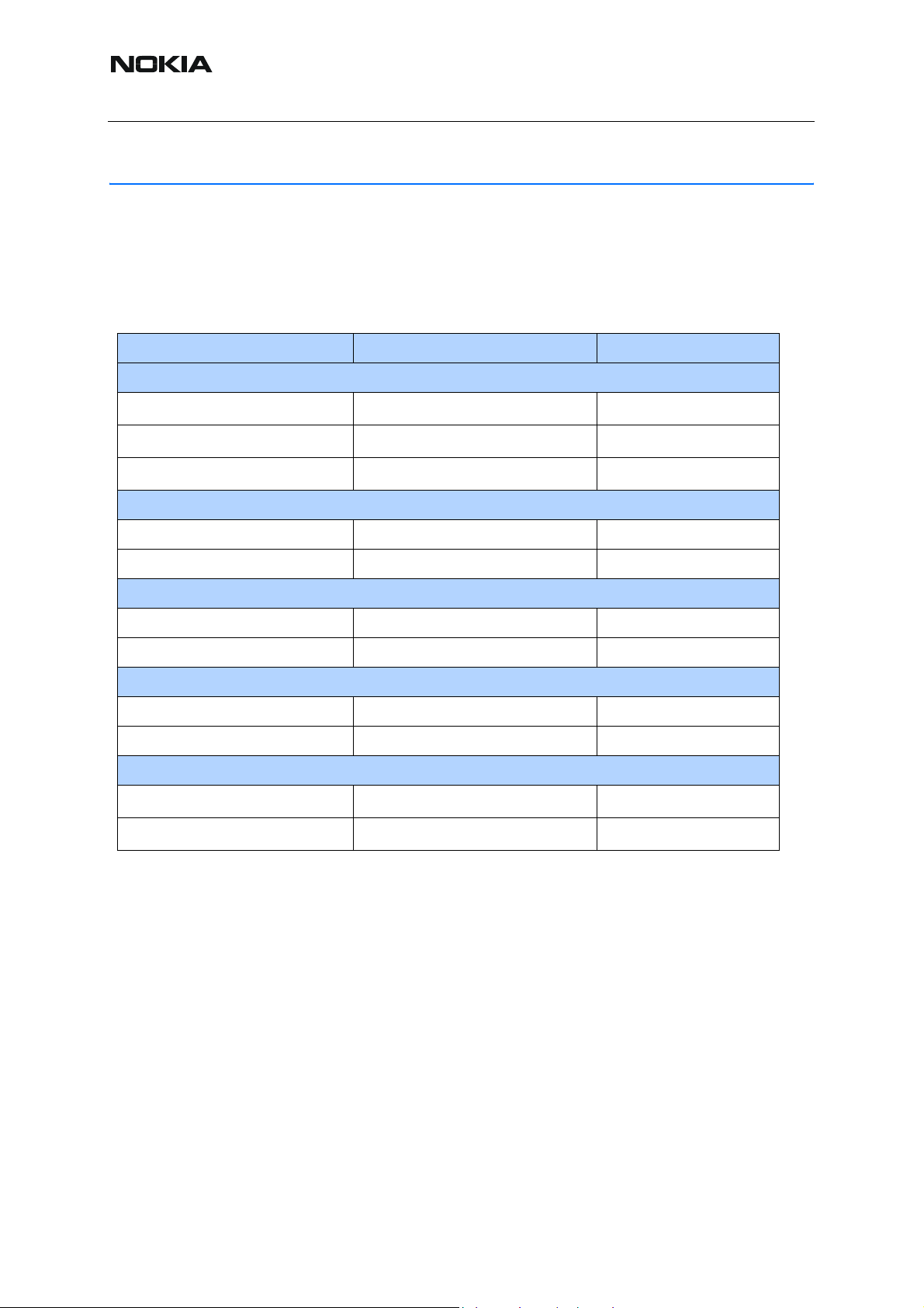
Table of Contents
Page No
Abbreviations ......................................................................................................6
General Description............................................................................................9
Feature list ......................................................................................................... 9
HW specific features: ....................................................................................... 9
UI features .......................................................................................................9
Technical Specifications .................................................................................. 10
Normal and extreme voltages.......................................................................... 10
Temperature conditions................................................................................... 10
Humidity........................................................................................................... 11
Vibration........................................................................................................... 11
ESD strength.................................................................................................... 11
HW Architecture Description ...........................................................................12
GSM Cellular Engine .....................................................................................12
RTC Circuitry .................................................................................................12
Zocus .............................................................................................................13
Power Management .......................................................................................... 14
HW reset switch............................................................................................... 14
Safety protected battery mode .......................................................................14
UEMEK............................................................................................................ 15
Internal regulator.............................................................................................. 16
External regulators........................................................................................... 17
VCORE SMPS ............................................................................................... 17
Bluetooth regulator .........................................................................................18
White Led Driver ............................................................................................ 18
Filter Components ..........................................................................................18
Power distribution ............................................................................................ 19
Battery connector............................................................................................. 20
Battery.............................................................................................................. 20
Charger interface............................................................................................. 21
System Connector ............................................................................................ 22
Interfaces ...........................................................................................................23
Camera............................................................................................................ 23
SIM interface.................................................................................................... 23
Flash Pads Pattern ........................................................................................23
Connectivity....................................................................................................... 25
IrDA.................................................................................................................. 25
IrDA Tiku EDGE Interface .............................................................................. 25
ISSUE 1 11/04 COMPANY CONFIDENTIAL 3
Copyright © 2004 Nokia. All Rights Reserved.
Page 4

RM-14
Nokia Customer Care 7 - System Module
Audio..................................................................................................................26
Display unit ...................................................................................................... 26
Mounting ........................................................................................................26
Engine Interface .............................................................................................26
Keyboard/UI..................................................................................................... 26
UI module .......................................................................................................26
Rotator ...........................................................................................................27
Function during use .......................................................................................27
Slide switch...................................................................................................... 29
LED driver........................................................................................................ 29
Generel circuit description .............................................................................30
Driving display and UI backlight ..................................................................... 30
Driving RGB LED ........................................................................................... 30
RF Module Introduction.................................................................................... 31
RF Frequency Plan............................................................................................ 32
Regulators ......................................................................................................... 33
Power Distribution ............................................................................................35
RF Characteristics ............................................................................................ 36
RF Block Diagram . ............................................................................................ 38
Frequency Synthesizers................................................................................... 39
Receiver........................................................................................................... 39
Transmittter...................................................................................................... 39
Front end.......................................................................................................... 39
Power amplifier................................................................................................ 40
RF ASIC Helgo ................................................................................................ 41
AFC function.................................................................................................... 41
List of Figures
Page No
Fig 1 RTC supply circuit.......................................................................................11
Fig 2 Zocus Circuit ...............................................................................................12
Fig 3 HW Reset circuit .......................................................................................... 14
Fig 4 Power Supply Overview..............................................................................15
Fig 5 SIM Filtering.................................................................................................17
Fig 6 Power Distribution.......................................................................................18
Fig 7 The connector............................................................................................. 19
Fig 8 BL-8N Battery.............................................................................................. 19
Fig 9 Charger Circuit............................................................................................20
Fig 10 TIKU/UEMEK SIM Interface Connections................................................. 22
Fig 11 FINUI and LABEL I/F ................................................................................ 23
Fig 12 Schematic for UI module............................................................................ 25
4 COMPANY CONFIDENTIAL ISSUE 1 11/04
Copyright © 2004 Nokia. All Rights Reserved.
Page 5

RM-14
7 - System Module Nokia Customer Care
Fig 13 Function during use.................................................................................... 26
Fig 14 The switch................................................................................................. 28
Fig 15 LED driver................................................................................................. 29
Fig 16 Figure 13 RF Frequency Plan....................................................................31
Fig 17 Power distribution diagram......................................................................... 34
Fig 18 RF Block Diagram.....................................................................................37
Fig 19 Front end................................................................................................... 40
Fig 20 Power Amplifier.........................................................................................40
ISSUE 1 11/04 COMPANY CONFIDENTIAL 5
Copyright © 2004 Nokia. All Rights Reserved.
Page 6
RM-14
Nokia Customer Care 7 - System Module
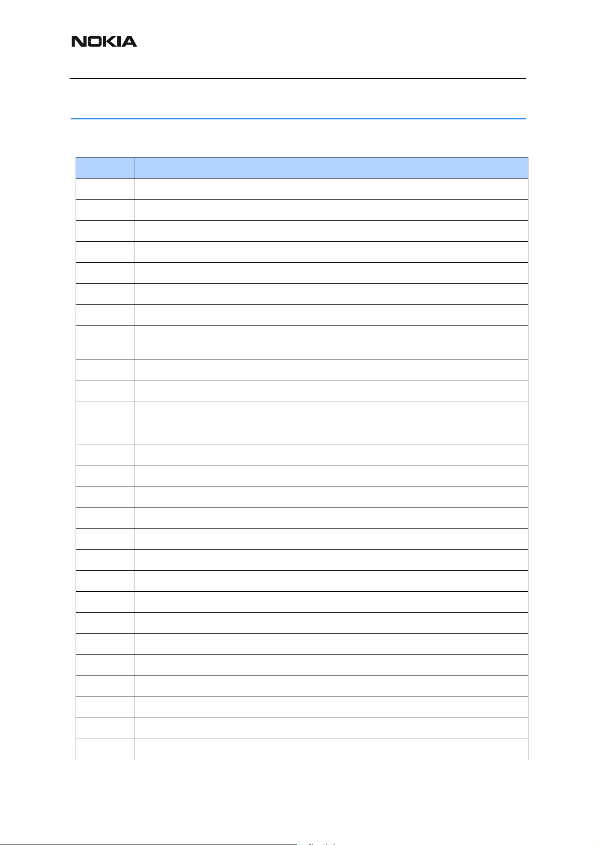
Abbreviations
Abbr. Description
ACI Accessory Control Interface
ADC Analog to digital converter
ASIC Application Specific Integrated Circuit
ASIP Application Specific Integrated Passive
ADSP Application DSP (expected to run high level tasks)
ARM Advanced RISC Machines
ARM915 ARM9TDMI Core, Caches, MMU’s
ARM925 ARM915 + WinCE Compatible MMU (WinCE is a hardwareprogrammed option
which will not be enabled for Tiku.)
BB Baseband
BB4.5 Common BaseBand 4.5 program
BC02 Bluetooth module by CSR
BL-8N Battery type.
BlueBird Bluetooth interface program to CSR.
CCP Compact Camera Port
CDSP Cellular DSP (expected to run low level tasks)
CIF Common Intermediate Format (352x288 pixels)
COF Chip on foil
COG Chip On Glass
CP Co-processor
CSR Cambridge Silicon Radio
CSTN Color Super Twisted Nematic
CTSI Clock Timing Sleep and Interrupt block of Tiku
DCT4.5 Digital Core Technology, generation 4.5
DSP Digital Signal Processor
DUT Device under test
EMC Electro Magnetic Compatibility
ESD Electro Static Discharge
6 COMPANY CONFIDENTIAL ISSUE 1 11/04
Copyright © 2004 Nokia. All Rights Reserved.
Page 7
RM-14
7 - System Module Nokia Customer Care
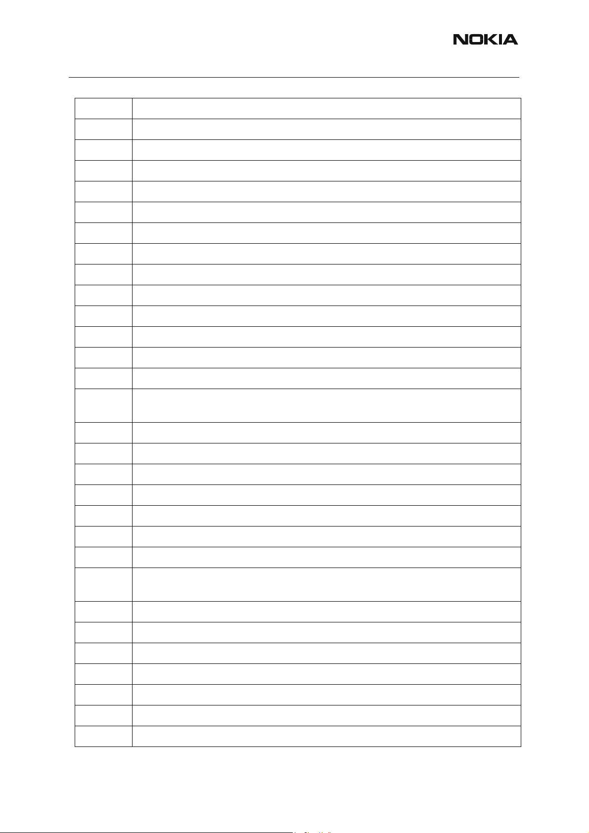
FR Full Rate
FSTN Film compensated Super Twisted Nematic
GSM Global System Mobile
HW Hardware
IF Interface
IHF Integrated Hands Free
IMEI International Mobile Equipment Identity
IR Infrared
IrDa Infrared Data Association
LCD Liquid Crystal Display
LDO Low Drop Out
LED Light Emitting Diode
LPRF Low Power Radio Frequency
MCU Microprocessor Control Unit
NTC Negative temperature Coefficient, temperature sensitive resistor used as an
temperature sensor.
PA Power Amplifier (RF)
PDA Personal Digital Assistant
PDRAM Program/Data RAM (on chip in Tiku)
Phoenix SW tool of DCT4.x
PUP General Purpose IO (PIO), USARTS and Pulse Width Modulators
PWB Printed Wired Board
RHEA TI bus from Lead3
RTC Real Time Clock, small circuitry that keeps track of updating the clock counter
and the calendar.
SARAM Single Access RAM
SIM Subscriber Identification Module
SW Software
SWIM Subscriber / Wallet Identification Module
TCXO Temperature Controlled Chrystal Oscillator
Tiku UPP (Universal Phone Processor), Official Tiku3G
TI Texas Instruments, American company
ISSUE 1 11/04 COMPANY CONFIDENTIAL 7
Copyright © 2004 Nokia. All Rights Reserved.
Page 8
RM-14
Nokia Customer Care 7 - System Module
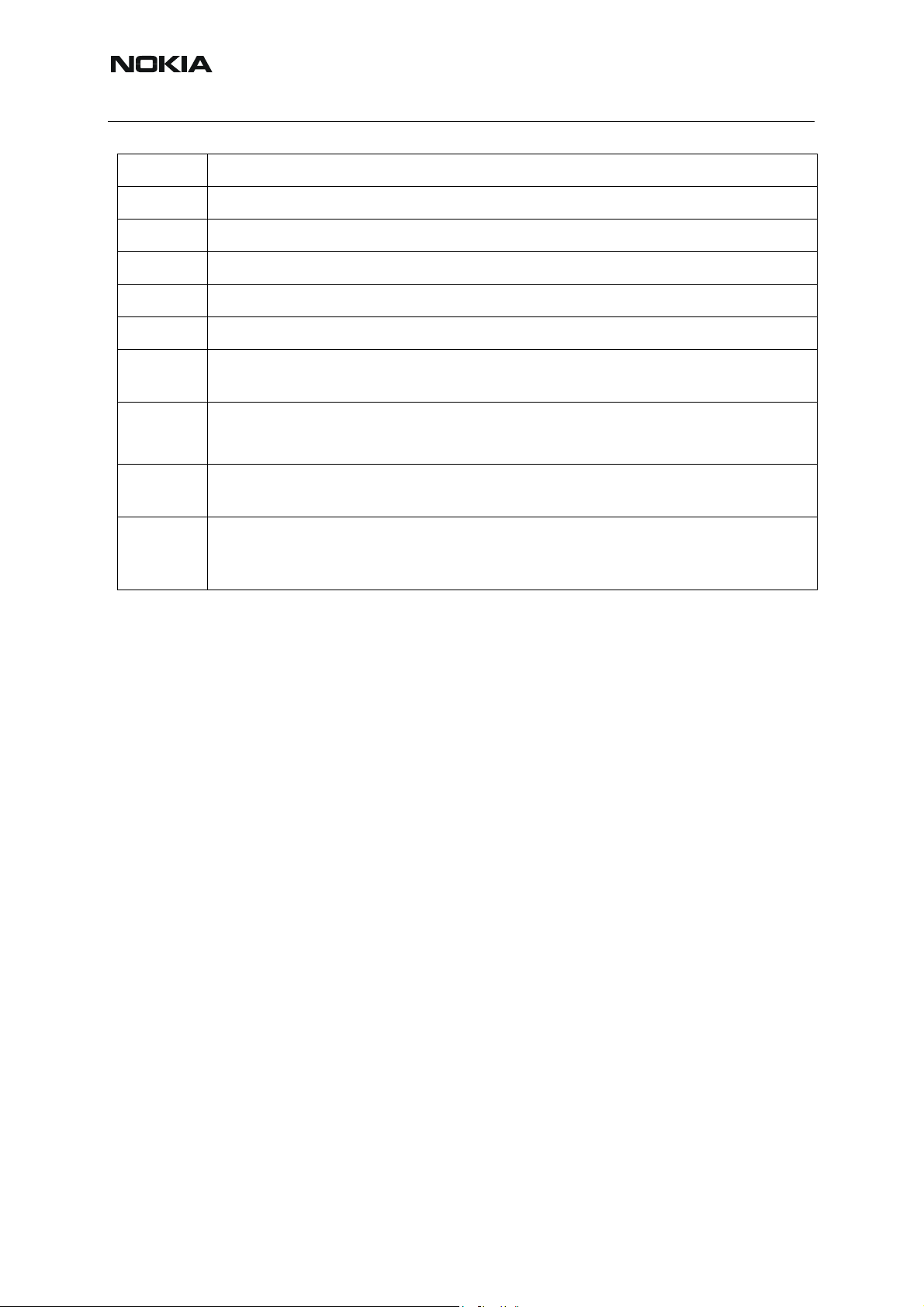
UEME Universal Energy Management Enhanced
UI User Interface
USB Universal Serial Bus
USWIM UMTS Subscriber / Wallet Identification Module
USIM UMTS Subscriber Identification Module
UPP Universal Phone Processor
UPP_WD2Communicator version of DCT4 system ASIC
VIA Versatile Interface Architecture (on chip bus structure)
Copper plated, drilled connection between layers in a PWB
WCDMA Wide Band Code Division Multiple Access, Third Generation (3G) of Mobile Tel-
ephones
Zocus Zero Ohm Current Sensor, Current measuring device. It measures the current
from and to the battery . It is used by the EM SW for calculating the left over pow-
er in the battery.
8 COMPANY CONFIDENTIAL ISSUE 1 11/04
Copyright © 2004 Nokia. All Rights Reserved.
Page 9

RM-14
7 - System Module Nokia Customer Care
General Description
■ Feature list
HW specific features:
- Monoblock phone
- Tripleband Engine (900, 1800, 1900)
- GPRS/EGPRS MSC 10 (4+1, 3+2)
- FR, EFR, AMR codecs
- Integrated VGA Camera
- Display: 208x104 pixels, transmissive and mirror (on film) effect
- MMS (Multi Media Messaging), Java MIDP2.0, SyncML1.1.1 and X-HTML
- Intergrated MP3 file support
- Bluetooth
- IR
- FM Radio
- IHF
- Rotator with limited UI input keys: Upper Soft Key, Lower Soft Key, SEND/END keys
- Mono (Plug'n'play) Accessory support
- Slide for receiving call
- Fixed battery
UI features
Bearers supported:
− EDGE
−CSD, HSCSD
−GPRS
−Bluetooth
ISSUE 1 11/04 COMPANY CONFIDENTIAL 9
Copyright © 2004 Nokia. All Rights Reserved.
Page 10
RM-14
Nokia Customer Care 7 - System Module
Technical Specifications
These figures are a summary of the SPR-requirements.
■ Normal and extreme voltages
Following voltages are assumed as normal and extreme voltages for used battery:
Table 1: Normal and extreme voltages
Voltage Voltage [V] Condition
General Conditions
Nominal voltage 3.90
a
Lower extreme voltage 3.3
Higher extreme voltage 4.30
HW Shutdown Voltages
Vmstr+ 2.1 ± 0,1 Off to on
Vmstr- 1.9 ± 0,1 On to off
SW Shutdown Voltages
Sw shutdown 3.1 In call
Sw shutdown 3.2 In idle
Min Operating Voltage
Vcoff+ 3.1 ± 0,1 Off to on
Vcoff- 2.8 ± 0,1 On to off
HW-Reset Demands
Min 1.0V
Max --
a. The nominal voltage is defined as being 15% higher than lower extreme voltage. TA will test with this nominal voltage
at an 85% range (0.85 x 3.9V ª 3.3V)
b. This limit is set to be above SW shutdown limit in TA.
b
c
d
c. During fast charging of an empty battery, this voltage might exceed this value. Voltages between 4.20 and 4.60 might
appear for a short while
d. The minimum Battery cell voltage required for the reset circuitry to turn on. This is not confirmed by measures at pt..
■ Temperature conditions
(1) Operational temperature range (all specifications met within this range)
–10°C +55°C
(2) Functional temperature range (Reduced performance)
–30°C +70°C
(3) Storage temperature range:
–30°C +85°C
10 COMPANY CONFIDENTIAL ISSUE 1 11/04
1
Copyright © 2004 Nokia. All Rights Reserved.
Page 11

RM-14
7 - System Module Nokia Customer Care
Temperatures at –10°C, +25°C and +55°C are used for cpk analysis.
The baseband module complies with the SPR4 Operating Conditions.
■ Humidity
Relative humidity range is 5...95%.
The BB module is not protected against water . Condensed or spla shed water might cause mal-
function. Any submerge of the phone will cause permanent damage. Long-term high humidity,
with condensation, will cause permanent damage because of corrosion.
The baseband module complies with the SPR4 Operating Conditions.
■ Vibration
The baseband module complies with the SPR4 Operating Conditions.
■ ESD strength
The baseband module complies with the SPR4 Operating Conditions.
ISSUE 1 11/04 COMPANY CONFIDENTIAL 11
Copyright © 2004 Nokia. All Rights Reserved.
Page 12
RM-14
Nokia Customer Care 7 - System Module
HW Architecture Description
GSM Cellular Engine
The BaseBand Engine consists of the TEMS (TikuEdge Memory Stacked Package) concept
and UEMEK. The TEMS concept combines all memory components in one package, which is
stacked on top of the TikuEdge. The memory combines 128Mbit NOR Flash, 512Mbit NAND
Flash and 128Mbit SDRAM in one package. The TikuEdge is also implemented in a stacked
package in which all pin connections are available on bottom pinout, and memory interface on
top pin out (POP I/F).
The energy manegement related part of the microBB4.5 engine is the UEMEK.
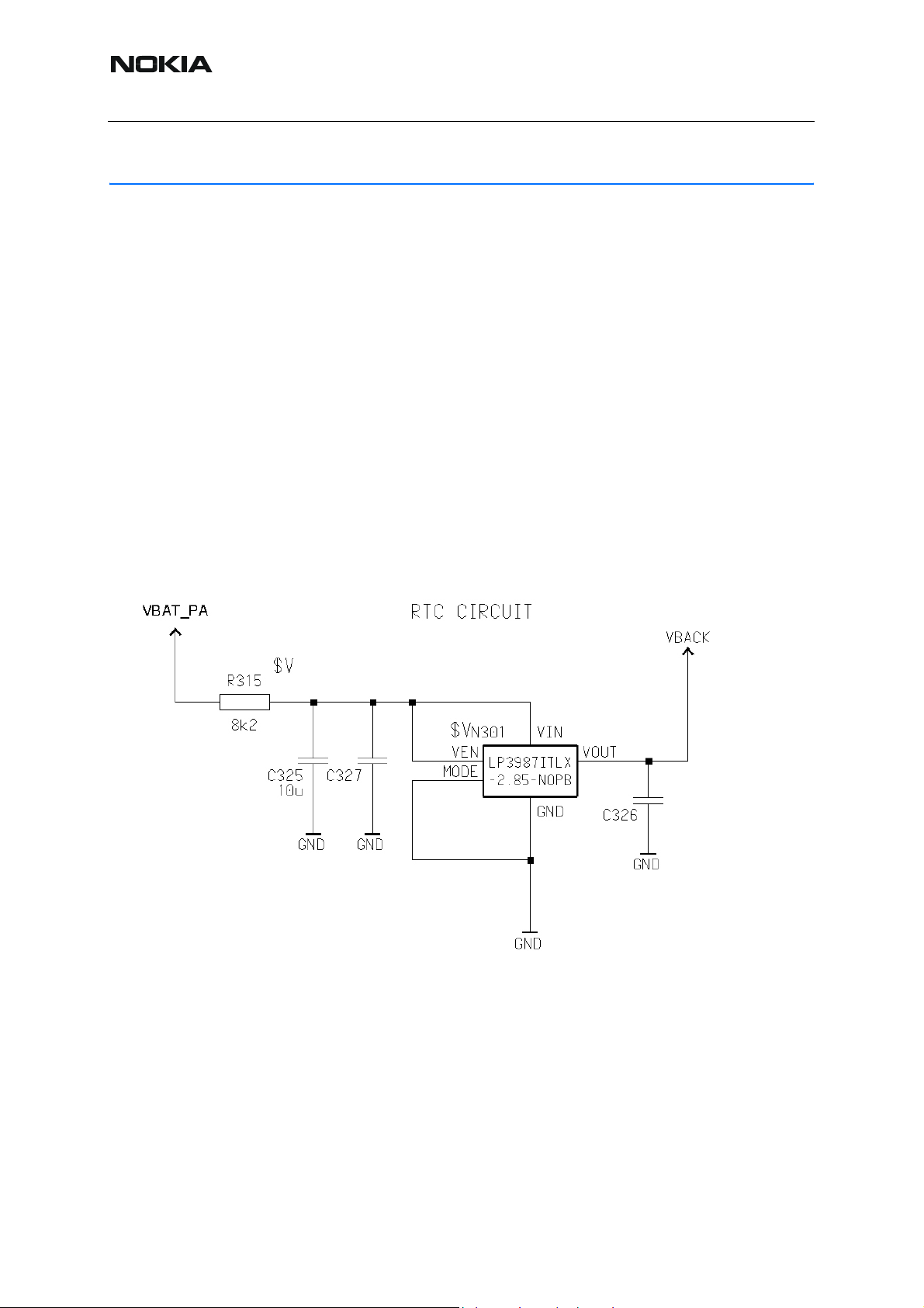
RTC Circuitry
Therefore a voltage regulator is used to supply the RTC circu it via the battery . The circu it looks
as follows:
Figure 1: RTC supply circuit
This is used in sleep mode where it is able to source 3mA. The supply VBAT_PA is byp assing
the HW switch, and therefore will have contact to the battery also whe n the SIM drawer is pulled
out.
The circuit will give a long back up time. Capacity on the battery when it has been discharged
to engine cut off (3,1V) is still 2.2mAh before battery voltage reaches 2,9V. This gives a back
up time of approx:
71 hours.
12 COMPANY CONFIDENTIAL ISSUE 1 11/04
Copyright © 2004 Nokia. All Rights Reserved.
Page 13
RM-14
7 - System Module Nokia Customer Care
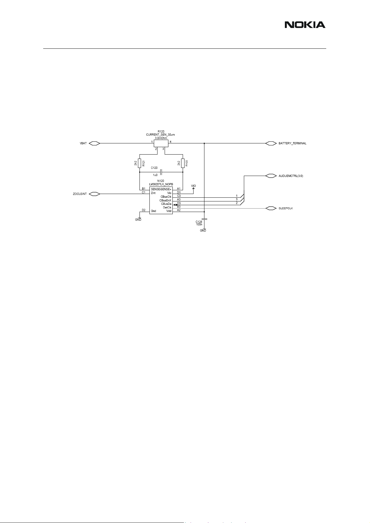
Zocus
The Zocus device (LM3820) is a precision current sensor, used by energy management software to determine the current consumption in the mobile phone.
Figure 2: Zocus Circuit
ISSUE 1 11/04 COMPANY CONFIDENTIAL 13
Copyright © 2004 Nokia. All Rights Reserved.
Page 14

RM-14
Nokia Customer Care 7 - System Module
Power Management
■ HW reset switch
Since the RM-14 project is equipped with a “fixed battery”, a need of a specific HW reset solution is required, since this is no longer possible by removing the battery. This request is meet
by the implementation of a power cut-of f switch that disconnects the battery power from the rest
of the phone. This switch is implemented by 2 P-Channel MOSFET’s inserted in the battery
power line.
RTC backup:
A minimum of 10 minutes power supplied to the RTC circuit is required.
Dead battery charge:
A battery safety circuit is protected by battery cell, which must be re-enabled.
Description:
The circuit depicted in HW Reset circuit-figure is connected to battery at “VBAT” and to the
phone at VBA T_OUT. The switch referred to as “SW” illustrates the switch, which enables power, supplied to the phone. This is implemented as a normally open switch in the SIM can. Its
function is to open when SIM-card is inserted and close whenever it’s extracted.
Beside of the PA-Module implementation, the rest of the phone will be powered from the
VBAT_OUT.
Safety protected battery mode
This mode implies a battery that has its cell disconnected from battery terminals by the batt eries own protection circuit .
When the protection circuit is disabled, the battery cell voltage is visible at the ba ttery terminals.
This means that the voltage of VBA T_OUT equals the battery cells whereas this must be higher
than the Gate-Source threshold voltage of Q1-2.
14 COMPANY CONFIDENTIAL ISSUE 1 11/04
Copyright © 2004 Nokia. All Rights Reserved.
Page 15

RM-14
7 - System Module Nokia Customer Care
Figure 3:HW Reset circuit
■ UEMEK
The UEMEK is providing the power for the phone. It consist of the following regulators:
− BB 8 voltage regulators
− RF 7 voltage regulators, 2 current regulators
The BB regulators in the UEMEK are controlled by MCUSW except VANA, VFLASH1, VIO,
which are controlled by the UEMEK itself. The RF regulators are controlled by DSPSW except
VR3, which is controlled by the UEMEK.
An external regulator (SMPS) provides the core voltage for the phone processor (T ikuEDGE).
ISSUE 1 11/04 COMPANY CONFIDENTIAL 15
Copyright © 2004 Nokia. All Rights Reserved.
Page 16

RM-14
Nokia Customer Care 7 - System Module
The inputs of the UEMEK regulators are filtered by a coil / capacitor filter. Some of the inputs
are joined together..
Figure below shows the connections in the different filters.
VIO regulator is overloaded in sleep mode (this issue is inherited from Nokia 6230). Due to
peak currents on display and SDRAM the maximum output current for VIO regulator (2mA) is
exceeded.
Figure 4: Power Supply Overview
Charger
Section
Charger
Connector
Charger
Filter
Fuse 1.5A
BATT
VBAT
Zocus
Battery
■ Internal regulator
LM2708
Regulator
LP3987
Regulator
HW Reset
VBAT_PA
Switch
VCORE
2,8V REG
VBAT
TO RF
Bluetooth
BC02
Tiku
PA-Module
VBATBB
LM2795,
White Led
Driver
Current
Regulator
Audio
PA
Legend:
UEMEK
EMC Section
Ext. components
Display
BLight
KBoard
BLight
RGB Led
Buzzer
Tiku PLL
Filter 1
Filter 2
Filter 3
Filter 4
Filter 5
Filter 6
Filter 7
VAUX1
Regulator
VAUX2
Regulator
VAUX3
Regulator
VFLASH1
Regulator
VCORE
Regulator
VANA
Regulator
VIO
Regulator
VSIM
Regulator
VR1A/B
Regulator
VR3
Regulator
VR2
Regulator
VR4
Regulator
VR5
Regulator
VR6
Regulator
VR7
Regulator
VAUX1
VAUX2
VAUX3
VFLASH1
VCORE_LIN
VANA
VIO
VSIM
VR1A/B
VR3
VR2
VR4
VR5
VR6
VR7
Not used
Not used
Not used
LCD, IrDA, FM radio,
Camera analog
Camera Dig
UEME audio, RF
{
RX/TX conv.
Flash, SDRAM, LCD i/
o, NUT i/o, TIKU i/o,
{
BT i/o, Zocus i/o
SIM
RF Section
RF Section
Enable for BT clock
RF Section
RF Section
RF Section
RF Section
RF Section
The following list shows the internal regulators:
Table 2: Internal Regulators
Name Voltage (V) Current (mA) Fil-
Comment
ter
Min Nom Max Max Sleep
Max
VANA 2.70 2.78 2.86 80 2 5uA minimum for stability.
Controlled by the UEMEK.
Disabled in Sleep mode.
VFLASH1 2.7
(2.61)
2.78 2.86
(2.95)
70 1.5 1 5uA minimum for stability.
Controlled by the UEMEK.
(Sleep indication)
16 COMPANY CONFIDENTIAL ISSUE 1 11/04
Copyright © 2004 Nokia. All Rights Reserved.
Page 17

RM-14
7 - System Module Nokia Customer Care
Name Voltage (V) Current (mA) Fil-
ter
Min Nom Max Max Sleep
Max
VIO 1.72 1.80 1.88 150 2 3 5uA minimum for stability.
VCORE
Camera
on
VAUX1 1.745
VAUX2 2.70 2.78 2.86 70 0.5 1 5uA minimum for stability.
VAUX3 2.70 2.78 2.86 20 0.5 1 5uA minimum for stability.
VSIM 1.745
VR1A/B 4.60 4.75 4.90 10 - 4 Disabled in Sleep mode. The
1.71 1.8 1.89 200 0.2 1 5uA minimum for stability.
2.91
2.91
1.80
3.0
1.80
3.00
1.855
3.09
1.855
3.09
50 0.5 1 Voltage level is set by
25 0.5 - 5uA minimum for stability.
Comment
Controlled by the UEMEK.
MCUSW is setting the voltage.
MCUSW.
maximum current is for 1 regulator active. If both are used,
maximum 5mA each.
VR2 2.70
(2.61)
VR3 2.70 2.78 2.86 20 - 4 100uA minimum for stability.
VR4 2.70 2.78 2.86 50 0.1 6 100uA minimum for stability.
VR5 2.70 2.78 2.86 50 0.1 7 100uA minimum for stability.
VR6 2.70 2.78 2.86 50 0.1 7 100uA minimum for stability.
VR7 2.70 2.78 2.86 45 - 7 100uA minimum for stability.
2.78
(2.78)
2.86
(2.95)
100 - 5 100uA minimum for stability.
Active during (Sleepmode).
Controlled by the UEMEK.
■ External regulators
VCORE SMPS
The VCORE regulator is based on the LM2708 step-down DC-DC converter . The regulator can
provide 350mA and can switch between 1.35 – 1.57V output voltag e. It can switch between low
power mode (Sleep) (linear mode) and full power mode (switched).
- Input voltage 2.7 – 5.5V
- Output voltage 1.35V – 1.57V
- External Sync input (PWM frequency between 500kHz and 750khz)
- Output current 517mA
ISSUE 1 11/04 COMPANY CONFIDENTIAL 17
Copyright © 2004 Nokia. All Rights Reserved.
Page 18

RM-14
Nokia Customer Care 7 - System Module
- Overload and thermal protection
Bluetooth regulator
An external regulator powers the BC02 module. The used regulator is a LP3987ITL by National
Semiconductor. The output voltage is 2.8V and the output current is 150mA continuously.
White Led Driver
A white led driver is implemented for display backlight and key_UI le’s. RGB Led Regulator
This regulator supplies the RGB led.
Filter Components
All connectors going to the “outside world” have filter components, ESD protection and EMC
reduction.
The Digital/Data lines on SIM have special d edicated filter ASIP . The belo w figure show the SIM
filtering.
Figure 5:SIM Filtering
The Audio circuit: Earpiece, IHF, internal microphone and external speaker are filtered with discrete components (common mode reduction coils, Varistors, caps and resistors), where as the
external microphone uses differential mode mic. ASIP.
The 16 UEMEK BB & RF regulators are specified to have a decoupling cap of 1 uF ±20%.
18 COMPANY CONFIDENTIAL ISSUE 1 11/04
Copyright © 2004 Nokia. All Rights Reserved.
Page 19

RM-14
7 - System Module Nokia Customer Care
■ Power distribution
The connection of various power connection can be seen in the following overview.
Figure 6: Power Distribution
HF
Speaker
Vibra
"On Key"
CHARGER
PAOUTN
ESD
PAOUTP
ESD
BuzzO
PwrOnX
ESD
VR1A 4.75V
VR1B 4.75V
VR2
2.78V
VR3
2.78V / 3.6V
VR4
2.78V / 3.6V
VR5
2.78V / 3.6V
VR6
2.78V / 3.6V
VR7
2.78V / 3.6V
RF Regulators BB Regulators
VRefRF02
VRefRF01
VBack
VCharOut
BTEMP
RF CODECS
AUDIO CODEC
DIGITAL
BLOCKS
DIGITAL
BLOCKS
VBack
BSI
LS
PURX
SleepClk
SleepX
VCharIn
UEMEK
2.78V VAUX2
2.78V
VAUX3
VANA2.78V
VFLASH1
2.78V
1.8/3.0V
VSIM
VAUX11.8/3.0V
VCORE1.0-1.8V
1.8V
1,8V VIO
KLight
DLight
CALLED
UEMRstX
Vibra
ESD
RGB Led
Display
illumination
LCD Driver
LED
driver
RGB
Reg
IR
Module
SIM
CCP
Camera
Parallel
Display
Keyb Light
Rotator
FM Radio
Battery
BL-8N
BATT
VBAT
VXO
ZOCUS-C
HW Reset
Sw
HELGO
RF
PA_Module
TIKU
EDGE Memory
Stacked
(TEMS)
RFClock
BC02
2.8V
LP3987
1.5V
VCORE
LM2708
NewVision Jinx
Power Distribution Diagram
Ver. 0.1
18.02.2004
CONFIDENTIAL
Copyright © 2002 Nokia Mobile Phones
ISSUE 1 11/04 COMPANY CONFIDENTIAL 19
Copyright © 2004 Nokia. All Rights Reserved.
Page 20

RM-14
Nokia Customer Care 7 - System Module
■ Battery connector
The battery connector has two pogo pins one for VBA T (Pin A) and one f or GND (Pin B). There
are no connections for either BTEMP or BSI. Hence the temperature is measured with a NTC
on PWB opposite side of battery.
The connector has a dynamic movement area of 0.6 - 2.1mm with a force of 2.3 – 0.3N respectivly.
Figure 7: The connector
■ Battery
Type:BL-8N
Technology:Li-Ion. 4.2V charging. 3.1V cut-off
Capacity:700 mAh
The battery pack is designed for RM-14 .
The BSI resistor is placed on the main PWB as RM-14 supports only one battery capacity. Fur-
ther a BSI connection is added to the Flash interface.
The battery temperature is measured by a NTC resistor placed on the main PWB, opposite to
the Battery.
Battery pack has an impedance of 130 - 150mΩ (0 – 45
Figure 8: BL-8N Battery
o
C).
20 COMPANY CONFIDENTIAL ISSUE 1 11/04
Copyright © 2004 Nokia. All Rights Reserved.
Page 21

RM-14
7 - System Module Nokia Customer Care
Inside the battery, an over-temperature and an over-voltage protection circuit are present. Op-
o
erational temperatures of battery are –20 – 70
C in discharge mode.
Care should be taken with the temperature. If the battery is charged above 60 degrees Celsius,
overheating might occur.
■ Charger interface
RM-14 conforms to the global NMP Charger Interface.
Charging is controlled by the UEMEK. The charger connection is through the system connector
interface. The RM-14 baseband is designed to support both 2- and 3-wire type chargers.
Figure 9: Charger Circuit
ISSUE 1 11/04 COMPANY CONFIDENTIAL 21
Copyright © 2004 Nokia. All Rights Reserved.
Page 22

RM-14
Nokia Customer Care 7 - System Module
System Connector
The system connector in RM-14 is a plug and play connector.
The Plug & Play system connector supports the fully differential DCT4, 4-wire audio/co ntrol interface which includes:
Audio
- 2 -wire fully differential mono audio
- 2-wire differential mic input
Detection/controlling
- Headint passive brake switch
Not supported is:
- Pins for 2 -wire charging in cradles
Table 3: DC Plug pinlist
PinNo Pin Name Description Voltage levels, Current Comment
2 CHARGE Charger input 0-16,9V, 0,85A Max Voltage Peak from
AC-7 used.
1 GND Ground 0,85A
22 COMPANY CONFIDENTIAL ISSUE 1 11/04
Copyright © 2004 Nokia. All Rights Reserved.
Page 23

RM-14
7 - System Module Nokia Customer Care
Interfaces
■ Camera
The module has only one operating mode: Bayer mode (raw pixel data output). Thus viewfinder, video streaming, colour correction, white balance etc. must be handled in software.
■ SIM interface
The engine first tries to contact SIM card with 1.8V. If no response is given, 3.0V supply is tried
instead.
The whole SIM interface locates in two asics; TIKU and UEMEK.
Figure 10: TIKU/UEMEK SIM Interface Connections
SIM
C5C6C7
C1C2C3
UEMEK
SIMIF Block
C8
C4
SIMData
SIMClk
SIMRst
VSIM
BSI
GND GND
Data
SIMClk
SIMIO
UEMEK
Dig. Logic
Tiku
Data
SIMClk
SIMIO
UIF Block
UEMInt
CBusDa
CBusEnX
CBusClk
The internal clock frequency from the CTSI Block is 13 MHz in GSM.
Flash Pads Pattern
These are accessed through the SIM Can by removing the SIM draw’. There is no access to
the battery connector and hereby the battery, through this interface connection. The battery
cannot be charged when the POS adapter is inserted.
The power is supplied to the Engine for purposes of power supply during flashing only. Also,
this interface is used for flashing when battery is inserted, and hereby the I/F ensures that there
is no connection to battery.
ISSUE 1 11/04 COMPANY CONFIDENTIAL 23
Copyright © 2004 Nokia. All Rights Reserved.
Page 24

RM-14
Nokia Customer Care 7 - System Module
Figure 11: FINUI and LABEL I/F
24 COMPANY CONFIDENTIAL ISSUE 1 11/04
Copyright © 2004 Nokia. All Rights Reserved.
Page 25

RM-14
7 - System Module Nokia Customer Care
Connectivity
■ IrDA
RM-14 suppports data connectivity via the Infra Red lin k. The IR interface is integrated into the
TIKU and the main external component is the IR module. The datarate supported will be
1.152Mbit. The circuit around the module is the same as in Nokia 6230. However, since the IR
window due to design reasons is lifted in relations to the PWB an lig htguide has to connect the
IR light and the IR window . Thus the u p firing module TFDU5307 from Vishay has been selected, instead of the one used in Nokia 6230.
IrDA Tiku EDGE Interface
This interface receives data from, and transmits data to peripheral equipment. It transforms serial data to parallel data, for the MCU or DSP, and vice versa.
ISSUE 1 11/04 COMPANY CONFIDENTIAL 25
Copyright © 2004 Nokia. All Rights Reserved.
Page 26
RM-14
Nokia Customer Care 7 - System Module
Audio
The audio and vibrator functions are specified UI
■ Display unit
Mounting
The Display Unit interface is a parallel interface.
Engine Interface
A 24-pin connector provides the interface between the Display Unit and the Engine PWB.
■ Keyboard/UI
UI module
RM-14 is instead of a traditional alphanumerical keyboard equipped with a rotator. The user
interface is thus the rotator + 5 keys (upper soft key, lower soft key, send, end/power, select).
All this combined with backlight is called UI module.
The schematic of the complete UI-module can be seen below.
Figure 12: Schematic for UI module
ASIC
PWB
LED driver
circuit
10 line EMI filter
1kOhm
16 pin UIconnector
16 line
flexpiece
LED1+
Upper Soft Key
Lower Soft Key____________________________
TIKU P(00) row0
TIKU P(01) row1
TIKU P(02) row2
Send
LED2+
Rotator module
LED1-
GND
Sel
220 Ohm
(0402 comp)
1nF
(0402 comp)
PWRONX
LED2-
GND
68 Ohm
(0402 comp)
CL-510S-WD-D-T
SOFT LEFT SOFT RIGHT
SEND END
68 Ohm
(0402 comp)
Citizen
SwitchA
Select
SwitchC
CL-510S-WD-D-T
Citizen
SwitchB
5V6/15V/0J05
5V6/15V/0J05
(1825127)
Varistor
AVX TVS
(1825127)
Varistor
AVX TVS
In the middle of the rotator there is a select key. On top of this 4 keys are present, these are:
- Send
- End/power-key
26 COMPANY CONFIDENTIAL ISSUE 1 11/04
Copyright © 2004 Nokia. All Rights Reserved.
Page 27

RM-14
7 - System Module Nokia Customer Care
- Upper soft key
− Lower soft key
These are implemented so that they can be pressed (and detected) simultaneously.
The powerkey is implemented in the END key. Therefore this will be connected to the
PWRONX pin on the UEME.
Rotator
The connections from the rotator module (including keys) to the engine are:
Function Connecting IC Pin Level pressed/
unpressed
Upper soft key TIKU GPIO2 (col0) 0/Open
Lower soft key TIKU GPIO3 (col1) 0/Open
Select TIKU GPIO13 0/Open
Switch A TIKU GPIO10 -Switch B TIKU GPIO9 -Switch C TIKU GPIO8 -Send TIKU GPIO4 0/Open
End/Power UEME PWRONX 0/Open
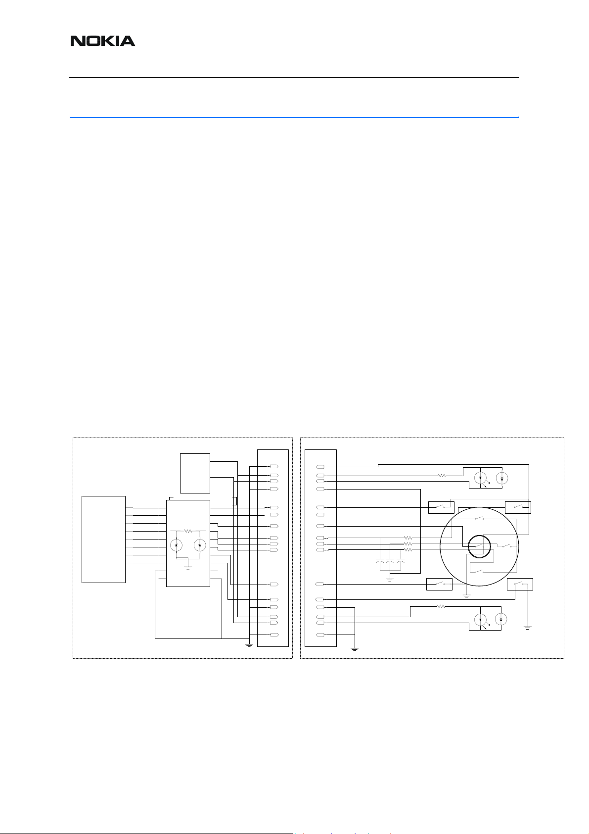
Function during use
This consists of 3 switches which during rotation open and close in the following pattern:
Figure 13:Function during use
ISSUE 1 11/04 COMPANY CONFIDENTIAL 27
Copyright © 2004 Nokia. All Rights Reserved.
Page 28

RM-14
Nokia Customer Care 7 - System Module
In the following:
-contacts in rotator are CAPITAL LETTERS
-pins on TIKU are corresponding lowercase letters (Thus switch A corresponds to pin A on
TIKU).
If the system has been initalized following routine is present (starting at point 1):
System has enabled pin c (driven low), a and b are disabled (pulled high).
Pos. 1: Contact A and B are closed, C is open (pin a = hi, b = hi, c = lo).
Between 1 & 2: Rotating the wheel CW causes:
Contact A to open => Now only B is closed, (pin a = hi, b = hi, c = lo).
Pos. 2: Rotating further CW causes:
C to close => now B and C is closed, This causes a low interrupt on pin b (pin a = hi, b = lo, c
= lo).
New state in SW is set: (pin a = lo, b = hi, c = hi). Now ready for next step.
Between 2 & 3: Rotating further CW causes:
B to open => now only C is closed, (pin a = lo, b = hi, c = hi).
Pos. 3: Rotating further CW causes:
A to close => Now A and C are closed. This causes a low interrupt on pin c (pin a = lo, b = hi,
c = lo).
New state in SW is set: (pin a = hi, b = lo, c = hi). Now ready for next step.
Between 3 & 1: Rotating further CW causes:
contact C to open => Now only A is closed.
Pos.1: This is similar to the first position 1. The pattern is repeated.
This pattern will go on as long as the rotator is turned CW, and the switches open and close
regulairy.
This means:
-In between steps only one switch is closed. This switch stays closed while the 2 other are
changing state.
-Every time a switch closes a low interrupt is generated.
-When going CCW the same pattern will happen, but in opposite order.
-Every time an interrupt is generated a new state has to be set.
-If a false state occurs, initalization routine has to be run until a correct state is reached.
28 COMPANY CONFIDENTIAL ISSUE 1 11/04
Copyright © 2004 Nokia. All Rights Reserved.
Page 29

RM-14
7 - System Module Nokia Customer Care
Whether the rotator movement is CW (down) or CCW (up) can thus b e decoded by comparing
the interrupt pin with the stage of the last interrupt.
■ Slide switch
A switch is needed to detect the position of the slide.
Connection to the engine:
Connecting
pin
AuxDet UEME Output from Hall IC tells if slide is open or
This switch is implemented with a hall IC and a magnet. The hall IC is SH248CSP from Samsung.
Connecting ICFunction Open/
Closed
1/0
closed
Figure 14: The switch
The signal from the Hall IC is connected to the analog keyboard input (AuxDet) in the UEME,
as this also is an interrupt input. This allows the phone to wake up, by opening the phone.
Analog keyboard input is used due to interrupt possibilities and because the Hall IC requires a
minimum supply voltage of 2.7V.
The Hall solution requires a magnet, which is placed on top of Ha ll-IC, and is moved away from
the sensor with the moving mechanics, thus making a change of the magnetic field. The magnet has the dimensions 5x3x1 mm and is mounted in the top of the phone in the sliding part.
ISSUE 1 11/04 COMPANY CONFIDENTIAL 29
Copyright © 2004 Nokia. All Rights Reserved.
Page 30

RM-14
Nokia Customer Care 7 - System Module
■ LED driver
The general LED driver circuit looks as follows:
Figure 15: LED driver
Generel circuit description
The circuit is build around LM2795(NMP code: 4341425. This is a switched capacitor type step
up converter. It has 5 outputs. 4 of them are mirrored current sources (D1-D4), and the 5
the output from the chargepump(Pout).
th
is
Driving display and UI backlight
The mirrored current sources are used to drive the display backlight (D1-D3), and the backlight(D4) to the UI-module (rotator).
Driving RGB LED
The Pout output (from the chargepump) is fed to the RGB LED’s.
30 COMPANY CONFIDENTIAL ISSUE 1 11/04
Copyright © 2004 Nokia. All Rights Reserved.
Page 31

RM-14
7 - System Module Nokia Customer Care
RF Module Introduction
The RF module performs the necessary high frequency operations of the EGSM900/
GSM1800/GSM1900 tripleband (EDGE) engine in the RM-14 product.
Both the transmitter and receiver have been implemented by using direct conversion architecture, which means that the modulator and demodulator operate at the channel frequency.
The core of the RF is an application-specific integrated circuit, Helgo. Another core component
is a power amplifier module, which includes two amplifier chains, one for EGSM900 and the
other for GSM1800/GSM1900.
Other key components include:
• 26 MHz VCTCXO for frequency reference
• 3296-3980 MHz SHF VCO (super high frequency voltage controlled oscillator)
• front end module comprising a RX/TX switch and two RF bandpass SAW filters
• three additional SAW filters
The control information for the RF is coming from the baseband section of the engine through
a serial bus, referred later on as RFBus. This serial bus is used to pass the information about
the frequency band, mode of operation, and synthesizer channel for the RF.
In addition, exact timing information and receiver gain settings are transferred through the RFBus. Physically, the bus is located between the baseband ASIC called TIKU and Helgo.
The RF circuitry is located on both sides of the 8 layer PWB.
EMC leakage is prevented by using metal cans. The RF circuits are separated to four blocks:
− FM radio.
−PA, front end module and VCTCXO.
− Helgo RF IC, baluns and balanced filters.
− VCO
The baseband circuitry is located on both side of the board, which is shielded with a meallized
frame and ground plane of the UI-board.
ISSUE 1 11/04 COMPANY CONFIDENTIAL 31
Copyright © 2004 Nokia. All Rights Reserved.
Page 32

RM-14
Nokia Customer Care 7 - System Module
RF Frequency Plan
RF frequency plan is shown below. The VCO operates at the channe l frequen cy multiplie d b y
two or four depending on the frequency band of operation.
Figure 16: RF Frequency Plan
32 COMPANY CONFIDENTIAL ISSUE 1 11/04
Copyright © 2004 Nokia. All Rights Reserved.
Page 33

RM-14
7 - System Module Nokia Customer Care
Regulators
The transceiver baseband section has a multi function analog ASIC, UEM, which contains
among other functions six pieces of 2.78 V linear regulators and a 4.8 V switching regulator.
The seven regulators are named VR1 to VR7. VrefRF01 and VrefRF02 are used as the reference voltages for the Helgo, VrefRF01 (1.35V) for the bias reference and VrefRF02 (1.35V) for
the RX ADC (analog-to-digital converter) reference.
The regulators (except for VR7) are connected to the Helgo.
List of the needed supply voltages
Volt. Source Load
VR1 PLL charge pump (4.8 V)
VR2 TX modulators, VPECTRL3s (ALC), driver
VR3 VCTCXO, synthesizer digital parts
VR4 Helgo pre-amps, mixers, DtoS
VR5 dividers, LO-buffers, prescaler
VR6 LNAs, Helgo baseband (Vdd_bb)
VR7 VCO
VrefRF01 ref. Voltage for Helgo
VrefRF02 ref. Voltage for Helgo
Vbatt PA
Typical Current Consumption
The table below shows the typical current consumption in different operation modes.
Operation mode Current consumption Notes
Power OFF < 10 uA
RX, EGSM900 75 mA, peak
RX, GSM1800/
GSM1900
ISSUE 1 11/04 COMPANY CONFIDENTIAL 33
70 mA, peak
Copyright © 2004 Nokia. All Rights Reserved.
Page 34

RM-14
Nokia Customer Care 7 - System Module
TX, power level 5,
EGSM900
TX, power level 0,
GSM1800/GSM1900
1700 mA, peak
1000 mA, peak
34 COMPANY CONFIDENTIAL ISSUE 1 11/04
Copyright © 2004 Nokia. All Rights Reserved.
Page 35

RM-14
7 - System Module Nokia Customer Care
Power Distribution
Power Distribution Diagram
Figure 17:Power distribution diagram
ISSUE 1 11/04 COMPANY CONFIDENTIAL 35
Copyright © 2004 Nokia. All Rights Reserved.
Page 36

RM-14
Nokia Customer Care 7 - System Module
RF Characteristics
Main RF Characteristics
Parameter Unit and value
Cellular system EGSM900/GSM1800/GSM1900
RX Frequency range EGSM900: 925 ... 960 MHz
GSM1800: 1805...1880 MHz
GSM1900: 1930...1990 MHz
TX Frequency range EGSM900: 880 ... 915 MHz
GSM1800: 1710 ...1785 MHz
GSM1900: 1850 …1910 MHz
Duplex spacing EGSM900: 45 MHz
GSM1800: 95 MHz
GSM1900: 80 MHz
Channel spacing 200 kHz
Number of RF channels EGSM900: 174
GSM1800: 374
GSM1900: 300
Output Power EGSM900: GSMK 5…33 dBm
EGSM900: 8-PSK 5…27 dBm
GSM1800: GSMK 0…30 dBm
GSM1800: 8-PSK 0…26 dBm
GSM1900: GSMK 0…30 dBm
GSM1900: 8-PSK 0…26 dBm
Number of power levels GMSK EGSM900: 15
GSM1800: 16
GSM1900: 16
Number of power levels 8-PSK EGSM900: 12
GSM1800: 14
GSM1900: 14
Transmitter Characteristics
Item Values (EGSM900/1800/1900)
Type Direct conversion, nonlinear, FDMA/TDMA
LO frequency range EGSM900: 3520...3660 MHz (4 x TX freq)
GSM1800: 3420...3570 MHz (2 x TX freq)
GSM1900: 3700...3820 MHz (2 x TX freq)
36 COMPANY CONFIDENTIAL ISSUE 1 11/04
Copyright © 2004 Nokia. All Rights Reserved.
Page 37
RM-14
7 - System Module Nokia Customer Care
Output power
(EGSM900/GSM1800/GSM1900)
Receiver Characteristics
Item Values, EGSM900/1800/1900
Type Direct conversion, Linear, FDMA/TDMA
LO frequencies EGSM900: 3700...3840 MHz (4 x RX freq)
Typical 3 dB bandwidth +/- 91 kHz
Sensitivity min. - 102 dBm (normal condition)
Receiver output level (RF level -95 dBm) 230 mVpp, single-ended I/Q signals to RX
GMSK 33/30/30 dBm
8-PSK 27/26/26 dBm
GSM1800: 3610...3760 MHz (2 x RX freq)
GSM1900: 3860...3980 MHz (2 x RX freq)
ADCs
ISSUE 1 11/04 COMPANY CONFIDENTIAL 37
Copyright © 2004 Nokia. All Rights Reserved.
Page 38

RM-14
Nokia Customer Care 7 - System Module
RF Block Diagram
The block diagram of the RF module can be seen in Figure 15. The detailed funct ional description is given in the following sections.
Figure 18: RF Block Diagram
Helgo
38 COMPANY CONFIDENTIAL ISSUE 1 11/04
Copyright © 2004 Nokia. All Rights Reserved.
Page 39

RM-14
7 - System Module Nokia Customer Care
Frequency Synthesizers
The VCO frequency is locked by a PLL (phase locked loop) into a stable frequency source given by a VCTCXO, which is running at 26 MHz.
The frequency synthesizer is integrated in Helgo except for the VCTCXO, VCO, and the loop
filter.
■ Receiver
Each receiver path is a direct conversion linear receiver. From the antenna the received RFsignal is fed to a front-end module where a diplexer first divides the signal to two separate p aths
according to the band of operation: either lower, EGSM900 or upper, GSM1800/GSM1900
path.
Most of the receiver circuitry is included in Helgo.
■ Transmittter
The transmitter consists of two final frequency IQ-modulators and power amplifiers, for the lower and upper bands separately, and a power control loop. The IQ-modulators are integrated in
Helgo, as well as the operational amplifiers of the power control loop. The two power amp lifiers
are located in a single module with power detector.
■ Front end
The front end features include:
- Antenna 50 ohm input
- RX EGSM900 balanced output
- RX GSM1800 balanced output
- RX GSM1900 single ended output
- TX GSM900 single ended 50 ohm input
- TX GSM1800/GSM1900 single ended 50 ohm input
- 3 control lines from the Helgo
ISSUE 1 11/04 COMPANY CONFIDENTIAL 39
Copyright © 2004 Nokia. All Rights Reserved.
Page 40

RM-14
Nokia Customer Care 7 - System Module
Figure 19: Front end
■ Power amplifier
The power amplifier features include:
50 ohm input and output, EGSM900 and GSM1800/GSM1900
Internal power detector
GMSK and EDGE mode
Figure 20: Power Amplifier
40 COMPANY CONFIDENTIAL ISSUE 1 11/04
Copyright © 2004 Nokia. All Rights Reserved.
Page 41

RM-14
7 - System Module Nokia Customer Care
■ RF ASIC Helgo
The RF ASIC features include
Balanced I/Q demodulator and balanced I/Q modulator
Power control operational amplifier, acts as an error amplifier
The signal from VCO is balanced, frequencies 3296 to 3980 MHz
Low noise amplifiers (LNAs) for EGSM900 and GSM1800 are integrated.
The Helgo can be tested by test points only.
■ AFC function
AFC is used to lock the transceiver’s clock to the frequency of the base station.
ISSUE 1 11/04 COMPANY CONFIDENTIAL 41
Copyright © 2004 Nokia. All Rights Reserved.
Page 42

RM-14
Nokia Customer Care 7 - System Module
[This page left intentionally blank]
42 COMPANY CONFIDENTIAL ISSUE 1 11/04
Copyright © 2004 Nokia. All Rights Reserved.
 Loading...