

Page 1

Nokia Customer Care
SERVICE
MANUAL
[NMP Part No. 9236149]
RM-17
Nokia 7260
Mobile Terminal
COMPANY CONFIDENTIAL
ISSUE 1 09/2004
Copyright © 2004 Nokia. All Rights Reserved.
Page 2
Nokia Customer Care
Amendment Record Sheet
Amendment No Date Inserted By Comments
Issue 1 Sept 2004 M. Hautaniemi
ISSUE 1 09/2004 COMPANY CONFIDENTIAL 2
Copyright © 2004 Nokia. All Rights Reserved.
Page 3

Nokia Customer Care
Copyright © 2004 Nokia. All rights reserved.
Reproduction, transfer, distribution or storage of part or all of the contents in
this document in any form without the prior written permission of Nokia is prohibited.
Nokia, Nokia Connecting People and RM-17 are trademarks or registered
trademarks of Nokia Corporation. Other product and company names mentioned herein may be trademarks or tradenames of their respective owners.
Nokia operates a policy of continuous development. Nokia reserves the right
to make changes and improvements to any of the products described in this
document without prior notice.
Under no circumstances shall Nokia be responsible for any loss of data or income or any special, incidental, consequential or indirect damages howsoever caused.
The contents of this document are provided "as is". Except as required by applicable law, no warranties of any kind, either express or implied, including,
but not limited to, the implied warranties of merchantability and fitness for a
particular purpose, are made in relation to the accuracy, reliability or contents
of this document. Nokia reserves the right to revise this document or withdraw it at any time without prior notice.
The availability of particular products may vary by region.
IMPORTANT
This document is intended for use by qualified service personnel
only.
ISSUE 1 09/2004 COMPANY CONFIDENTIAL 3
Copyright © 2004 Nokia. All Rights Reserved.
Page 4

Please refer to the product’s user guide for instructions relating
to operation, care and maintenance including important safety
information. Note also the following:
Warnings:
1. IF THE DEVICE CAN BE INSTALLED IN A VEHICLE, CARE
MUST BE TAKEN ON INSTALLATION IN VEHICLES FITTED
WITH ELECTRONIC ENGINE MANAGEMENT SYSTEMS AND
ANTI-SKID BRAKING SYSTEMS. UNDER CERTAIN FAULT
CONDITIONS, EMITTED RF ENERGY CAN AFFECT THEIR
OPERATION. IF NECESSARY, CONSULT THE VEHICLE
DEALER/MANUFACTURER TO DETERMINE THE IMMUNITY
OF VEHICLE ELECTRONIC SYSTEMS TO RF ENERGY.
Nokia Customer Care
Warnings and Cautions
2. THE product MUST NOT BE OPERATED IN AREAS LIKELY TO
CONTAIN POTENTIALLY EXPLOSIVE ATMOSPHERES EG
PETROL STATIONS (SERVICE STATIONS), BLASTING
AREAS ETC.
3. OPERATION OF ANY RADIO TRANSMITTING EQUIPMENT,
INCLUDING CELLULAR TELEPHONES, MAY INTERFERE
WITH THE FUNCTIONALITY OF INADEQUATELY PROTECTED MEDICAL DEVICES. CONSULT A PHYSICIAN OR
THE MANUFACTURER OF THE MEDICAL DEVICE IF YOU
HAVE ANY QUESTIONS. OTHER ELECTRONIC EQUIPMENT
MAY ALSO BE SUBJECT TO INTERFERENCE.
Cautions:
1. Servicing and alignment must be undertaken by qualified personnel only.
2. Ensure all work is carried out at an anti-static workstation and
that an anti-static wrist strap is worn.
3. Ensure solder, wire, or foreign matter does not enter the telephone as damage may result.
4. Use only approved components as specified in the parts list.
5. Ensure all components, modules screws and insulators are correctly re-fitted after servicing and alignment. Ensure all cables
and wires are repositioned correctly.
ISSUE 1 09/2004 COMPANY CONFIDENTIAL 4
Copyright © 2004 Nokia. All Rights Reserved.
Page 5
Nokia Customer Care
For your safety
QUALIFIED SERVICE
Only qualified personnel may install or repair phone equipment.
ACCESSORIES AND BATTERIES
Use only approved accessories and batteries. Do not connect incompatible
products.
CONNECTING TO OTHER DEVICES
When connecting to any other device, read its user’s guide for detailed safety
instructions. Do not connect incompatible products.
ESD protection
Nokia requires that product service points have sufficient
ESD protection (against static electricity) when servicing
products.
Any product of which the covers are removed must be handled with ESD protection. The SIM card can be replaced
without ESD protection if the product is otherwise ready for
use.
To replace the covers ESD protection must be applied.
All electronic parts of the product are susceptible to ESD.
Resistors, too, can be damaged by static electricity discharge.
All ESD sensitive parts must be packed in metallized protective bags during shipping and handling outside any ESD
Protected Area (EPA).
Every repair action involving opening the product or handling the product components must be done under ESD
protection.
ESD protected spare part packages MUST NOT be
opened/closed out of an ESD Protected Area.
For more information and local requirements about ESD
protection and ESD Protected Area, contact your local
Nokia After Market Services representative.
ISSUE 1 09/2004 COMPANY CONFIDENTIAL 5
Copyright © 2004 Nokia. All Rights Reserved.
Page 6

Nokia Customer Care
Battery information
Note that a new battery's full performance is achieved only after two or three
complete charge and discharge cycles!
The battery can be charged and discharged hundreds of times but it will
eventually wear out. When the operating time (talk-time and standby time) is
noticeably shorter than normal, it is time to buy a new battery.
Use only batteries approved by the phone manufacturer and recharge the
battery only with the chargers approved by the manufacturer. Unplug the
charger when not in use. Do not leave the battery connected to a charger for
longer than a week, since overcharging may shorten its lifetime. If left unused
a fully charged battery will discharge itself over time.
Temperature extremes can affect the ability of your battery to charge.
For good operation times with Ni-Cd/NiMh batteries, discharge the battery
from time to time by leaving the product switched on until it turns itself off (or
by using the battery discharge facility of any approved accessory available
for the product). Do not attempt to discharge the battery by any other means.
Use the battery only for its intended purpose.
Never use any charger or battery which is damaged.
Do not short-circuit the battery. Accidental short-circuiting can occur when a
metallic object (coin, clip or pen) causes direct connection of the + and - terminals of the battery (metal strips on the battery) for example when you carry
a spare battery in your pocket or purse. Short- circuiting the terminals may
damage the battery or the connecting object.
Leaving the battery in hot or cold places, such as in a closed car in summer
or winter conditions, will reduce the capacity and lifetime of the battery. Always try to keep the battery between 15°C and 25°C (59°F and 77°F). A
phone with a hot or cold battery may temporarily not work, even when the battery is fully charged. Batteries' performance is particularly limited in temperatures well below freezing.
Do not dispose of batteries in a fire!
Dispose of batteries according to local regulations (e.g. recycling). Do not dispose as household waste.
ISSUE 1 09/2004 COMPANY CONFIDENTIAL 6
Copyright © 2004 Nokia. All Rights Reserved.
Page 7

Nokia Customer Care
Care and maintenance
The product is a product of superior design and craftsmanship and should be
treated with care. The suggestions below will help you to fulfil any warranty
obligations and to enjoy this product for many years.
Keep the phone and all its parts and accessories out of the reach of small
children.
Keep the phone dry. Precipitation, humidity and all types of liquids or moisture can contain minerals that will corrode electronic circuits.
Do not use or store the phone in dusty, dirty areas. Its moving parts can be
damaged.
Do not store the phone in hot areas. High temperatures can shorten the life
of electronic devices, damage batteries, and warp or melt certain plastics.
Do not store the phone in cold areas. When it warms up (to its normal temperature), moisture can form inside, which may damage electronic circuit
boards.
Do not drop, knock or shake the phone. Rough handling can break internal
circuit boards.
Do not use harsh chemicals, cleaning solvents, or strong detergents to clean
the phone.
Do not paint the phone. Paint can clog the moving parts and prevent proper
operation.
Use only the supplied or an approved replacement antenna. Unauthorised
antennas, modifications or attachments could damage the phone and may violate regulations governing radio devices.
All of the above suggestions apply equally to the product, battery, charger or
any accessory.
ISSUE 1 09/2004 COMPANY CONFIDENTIAL 7
Copyright © 2004 Nokia. All Rights Reserved.
Page 8

Nokia Customer Care
Company Policy
Our policy is of continuous development; details of all technical modifications
will be included with service bulletins.
While every endeavour has been made to ensure the accuracy of this document, some errors may exist. If any errors are found by the reader, NOKIA
MOBILE PHONES Business Group should be notified in writing.
Please state:
Title of the Document + Issue Number/Date of publication
Latest Amendment Number (if applicable)
Page(s) and/or Figure(s) in error
Please send to:
NOKIA CORPORATION
Nokia Mobile Phones Business Group
Nokia customer care
PO Box 86
FIN-24101 SALO
Finland
ISSUE 1 09/2004 COMPANY CONFIDENTIAL 8
Copyright © 2004 Nokia. All Rights Reserved.
Page 9

Nokia Customer Care
Table of Contents
1. General Information
2. Parts List and Component Layout
3. Service Software and Tuning Instructions
4. Service Tools
5. Disassembly Instructions
6(a). Baseband Troubleshooting Instructions
6(b). RF Troubleshooting Instructions
7. System Module
8. Schematics
ISSUE 1 09/2004 COMPANY CONFIDENTIAL 9
Copyright © 2004 Nokia. All Rights Reserved.
Page 10
Nokia Customer Care
1 - General Information
ISSUE 1 09/2004 COMPANY CONFIDENTIAL
Copyright © 2004 Nokia. All Rights Reserved.
Page 11

RM-17
Nokia Customer Care 1 - General Information
[This page intentionally blank]
2 COMPANY CONFIDENTIAL ISSUE 1 09/2004
Copyright © 2004 Nokia. All Rights Reserved.
Page 12

RM-17
1 - General Information Nokia Customer Care
Table of Contents
Page No
RM-17 Product Selection.................................................................................... 5
RM-17 product and modules.............................................................................. 5
Supported accessories ...................................................................................... 6
Environmental conditions................................................................................... 7
Transceiver features .......................................................................................... 7
ISSUE 1 09/2004 COMPANY CONFIDENTIAL 3
Copyright © 2004 Nokia. All Rights Reserved.
Page 13

RM-17
Nokia Customer Care 1 - General Information
[This page intentionally blank]
4 COMPANY CONFIDENTIAL ISSUE 1 09/2004
Copyright © 2004 Nokia. All Rights Reserved.
Page 14
RM-17
1 - General Information Nokia Customer Care
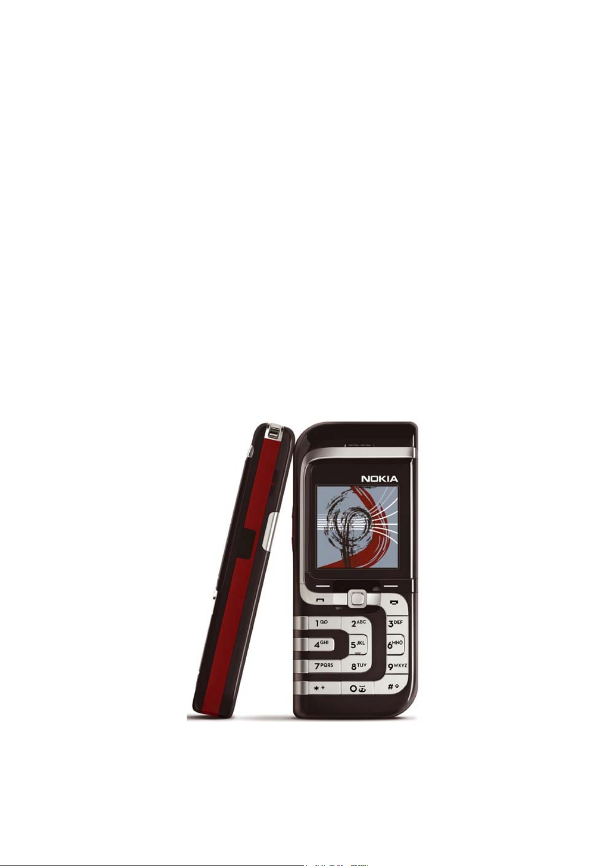
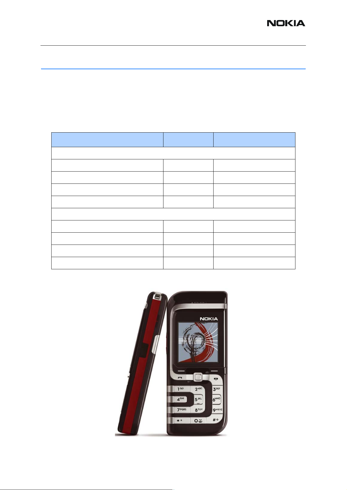
RM-17 Product Selection
The RM-17 is a triple band monoblock transceiver unit, designed for EGSM900, GSM1800 and
GSM1900 EDGE networks. It is a GSM900 phase 2, power class 4 (2W) transceiver and a
GSM1800/1900 power class 1 (1W) transceiver. It is also an EDGE900 power class E2 (0.5W/
27dBm) and an EDGE1800/1900 power class E2 (0.4W/26dBm) transceiver.
■ RM-17 product and modules
Name Type Code Material Code
EMEA transceiver
Basic transceiver RM-17 0513513
Printed Wiring Board (PWB) module 1DX 0202199
Mechanics module 0263526
Software module 8468457
APAC/China transceiver
Basic transceiver RM-17 0520146
Printed Wiring Board (PWB) module 1DX 0202199
Mechanics module 0263767
Software module 8460081
Figure 1: RM-17 transceiver
ISSUE 1 09/2004 COMPANY CONFIDENTIAL 5
Copyright © 2004 Nokia. All Rights Reserved.
Page 15
RM-17
Nokia Customer Care 1 - General Information
■ Supported accessories
Product
Type
Description Comment
AC-1 Retractable charger
ACP-7 E&A, APAC = Standard Charger,
Americas = Standard Travel Charger
ACP-8 E&A = Travel Charger,
APAC = Fast & Light Charger
ACP-12 Travel Charger
AD-5B Wireless Voice Adaptor
BHF-1 Headrest Handsfree
BL-5B Battery Eur/Afr & Apac
Battery France
Battery Americas
Battery China
Battery Brazil
DKU-5 Connectivity Adapter Cable
HDB-4 Boom Headset
English type label
French type label
English type label
Chinese type label
Portuguese type label
HDS-3 Stereo Headset
HS-3 Stereo Headset
HS-3W Wireless Headset
HS-5 Headset
HS-10 Retractable Headset
LCH-9 E&A, APAC = Mobile Charger
LCH-12 E&A, APAC = Mobile Charger
LPS-4 Inductive Loopset
HDA-10
PopPort
TM
to tty adapter
RX-3 Image Viewer
RX-4 Image Viewer
RX-11 Image Viewer
SU-4 Picture Frame
SU-5 TV Image Viewer
SU-7 Image Viewer
6 COMPANY CONFIDENTIAL ISSUE 1 09/2004
Copyright © 2004 Nokia. All Rights Reserved.
Page 16
RM-17
1 - General Information Nokia Customer Care
Product
Type
Description Comment
MD-1 Desk Stand
Carrying Pouch
Nokia Observation Camera
Note: No car kit support.
■ Environmental conditions
Environmental
Condition
Normal operation -10°C…+55°C Specifications fulfilled
Reduced performance +55°C…+70°C Operational only for short periods
No operation or storage <-30°C…>+80°C No storage outside these temperatures.
Charging allowed -5°C…+55°C
Ambient
Temperature
Notes
An operation attempt may cause permanent damage
■ Transceiver features
Transceiver main HW parts/features include:
• GPRS (Class 10) 3+2, 4+1
• EGPRS (Class 6) 3+1, 2+2
• HSCSD/CSD
• Integrated VGA camera
• Colour display (size: 27.5mmx27.5mm. 64K colours, high resolution (128x128)
active matrix.
• Internal triple band antenna (no connection for external antenna)
• 5-way joystick
• Integrated Hands Free (IHF) speaker
• DCT charger plug
• PopPort
• IrDa (infrared interface)
• Volume keys
Note: The RM-17 phone has high gloss paint. The target customer-group is expected to be very
sensitive to the appearance of the phone. Therefore, extra care must be taken when handling
the covers. Use gloves when touching the product.
TM
connector
ISSUE 1 09/2004 COMPANY CONFIDENTIAL 7
Copyright © 2004 Nokia. All Rights Reserved.
Page 17

RM-17
Nokia Customer Care 1 - General Information
[This page intentionally blank]
8 COMPANY CONFIDENTIAL ISSUE 1 09/2004
Copyright © 2004 Nokia. All Rights Reserved.
Page 18

Nokia Customer Care
2 - Parts Lists and
Component Layout
ISSUE 1 09/2004 COMPANY CONFIDENTIAL
Copyright © 2004 Nokia. All Rights Reserved.
Page 19

RM-17
Nokia Customer Care 2 - Parts Lists and Component Layout
[This page intentionally blank]
2 COMPANY CONFIDENTIAL ISSUE 1 09/2004
Copyright © 2004 Nokia. All Rights Reserved.
Page 20

RM-17
2 - Parts Lists and Component Layout Nokia Customer Care
Table of Contents
Page No
Exploded View of RM-17 .................................................................................... 5
Assembly parts .................................................................................................. 6
Variant parts....................................................................................................... 8
1dxa_55a PWB Module Parts List...................................................................... 9
1dxa_55a PWB component locator (top) ......................................................... 25
1dxa_55a PWB component locator (bot) ......................................................... 25
ISSUE 1 09/2004 COMPANY CONFIDENTIAL 3
Copyright © 2004 Nokia. All Rights Reserved.
Page 21

RM-17
Nokia Customer Care 2 - Parts Lists and Component Layout
[This page intentionally blank]
4 COMPANY CONFIDENTIAL ISSUE 1 09/2004
Copyright © 2004 Nokia. All Rights Reserved.
Page 22
RM-17
2 - Parts Lists and Component Layout Nokia Customer Care
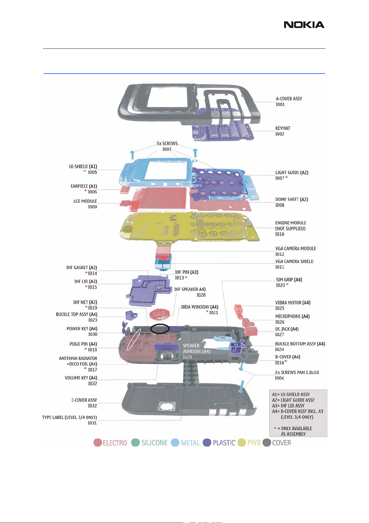
Exploded View of RM-17
ISSUE 1 09/2004 COMPANY CONFIDENTIAL 5
Copyright © 2004 Nokia. All Rights Reserved.
Page 23
RM-17
Nokia Customer Care 2 - Parts Lists and Component Layout
■ Assembly parts
Note: Do not use the following lists for spare part ordering. For ordering the spare parts please
refer to the related and updated Technical Bulletins.
ITEM/
CIRCUIT REF.
QTY PART NO PART NAME
I001 1 XXXXXXX A-COVER ASSY
I002 1 XXXXXXX KEYMAT
I003 5 6380209 SCREW M1.8X6 TORX PLUS
I004 2 6380191 SCREW PAN M1.8x10
1 9498016 UI-SHIELD ASSY
I005 1 - UI-SHIELD
I006 1 - EARPIECE
1 9481269 LIGHT Guide ASSY
I007 1 - LIGHT GUIDE
I008 1 9795310 DOME SHEET
I009 1 4850829 LCD MODULE EMEA
I009 1 4850827 LCD MODULE APAC
I010 1 - ENGINE MODULE
I011 1 9511279 VGA CAMERA SHIELD
I012 1 4858023 VGA CAMERA MODULE
1 9492010 B-COVER ASSY
1 0263525 IHF LID ASSY (I013 - I015)
I013 1 - IHF PIN
I014 1 - IHF GASKET
I015 1 - IHF LID
I016 1 - B-COVER
I017 1 - ANTENNA RADIATOR + DECO FOIL
6 COMPANY CONFIDENTIAL ISSUE 1 09/2004
Copyright © 2004 Nokia. All Rights Reserved.
Page 24
RM-17
2 - Parts Lists and Component Layout Nokia Customer Care
ITEM/
CIRCUIT REF.
I018 1 - POGO PIN
I019 1 - IHF-NET
I020 1 - SIM-GRIP
I021 1 - IRDA WINDOW
I022 1 9791424 VOLUME KEY
I023 1 9492044 BUCKLE TOP ASSY
I024 1 9492043 BUCKLE BOTTOM ASSY
I025 1 6800057 VIBRA MOTOR
I026 1 5140265 MICROPHONE
I027 1 5400243 DC-JACK
I028 1 5149007 IHF SPEAKER
I029 1 9480890 SPEAKER ADHESIVE
I030 1 9791420 POWER-KEY
QTY PART NO PART NAME
I031 1 9381484 TYPE LABEL
I032 1 XXXXXXX C-COVER ASSY
ISSUE 1 09/2004 COMPANY CONFIDENTIAL 7
Copyright © 2004 Nokia. All Rights Reserved.
Page 25
RM-17
Nokia Customer Care 2 - Parts Lists and Component Layout
■ Variant parts
ITEM QTY PART NO PART NAME
I001 1 9492039 A-Cover Assembly, black
I001 1 9492040 A-Cover Assembly, white
I002 1 9791425 Keypad Latin
I002 1 9797159 Keypad Arabic
I002 1 9797160 Keypad Hebrew
I002 1 9797161 Keypad Cyrillic
I002 1 9797162 Keypad Greek
I002 1 9797163 Keypad Stroke
I002 1 9797164 Keypad BoPoMoFo
I002 1 9797165 Keypad Thai
I002 1 9797167 Keypad Hindi
I002 1 9797168 Keypad Farsi
I002 1 9797169 Keypad Urdu
I031 1 9492041 C-Cover Assembly, black
I032 1 9492042 C-Cover Assembly, white
8 COMPANY CONFIDENTIAL ISSUE 1 09/2004
Copyright © 2004 Nokia. All Rights Reserved.
Page 26
RM-17
2 - Parts Lists and Component Layout Nokia Customer Care
1dxa_55a PWB Module Parts List
Note: Do not use the following lists for spare part ordering. For ordering spare parts, please refer
to the related and updated Technical Bulletins.
Item
A1101 9517379 Top N 5 SHIELD_DMC06961 BB-SHIELD ASSY
A1102 9517378 Top D 6 SHIELD_DMC06962 HELGO-SHIELD ASSY
A1103 9517377 Top F 3 SHIELD_DMC06963 PA-SHIELD ASSY
B2200 4510219 Top O 5 CRYSTAL_CX_4V CRYSTAL 32.768KHZ+-
B2402 5140265 Top S 5 MIC_KUB64MEY321 MIC MOD+HOLDER TOM-
C1470 2320778 Top K 6 0402C Chipcap X7R 10% 16V
C1471 2320546 Top K 6 0402C Chipcap 5% NP0 27p 50V normal,-
C1472 2320805 Top K 6 0402C CHIPCAP X5R 100N K
C1473 2320481 Top J 6 0603C CHIPCAP X5R 1U K 6V3
Product
Code
Location
Side X Y
Typ e Description
~~~
DMC06961 HDJ12
~~~
DMC06962 HDJ12
~~~
DMC06963 HDJ12
32.768kHz ~ ~
30PPM 9PF
~~~
AHAWK -42+-3DB
10n 16V normal,-
0402
100n 10V normal,-
10V 0402
1u0 6.3V normal,-
0603
10%,10%
5%,5%
10%,10%
10%,10%
C1474 2320546 Top J 7 0402C Chipcap 5% NP0 27p 50V normal,-
C1475 2320778 Top J 8 0402C Chipcap X7R 10% 16V
0402
C1476 2320778 Top K 6 0402C Chipcap X7R 10% 16V
0402
C1477 2320778 Top K 7 0402C Chipcap X7R 10% 16V
0402
C1478 2320778 Top J 6 0402C Chipcap X7R 10% 16V
0402
C1479 2320805 Top K 8 0402C CHIPCAP X5R 100N K
10V 0402
C1480 2320778 Top K 8 0402C Chipcap X7R 10% 16V
0402
C1481 2320481 Top L 8 0603C CHIPCAP X5R 1U K 6V3
0603
C1482 2320505 Top K 7 0603C CHIPCAP X5R 4U7 K 6V3
0603
C2001 2312243 Top M 5 0805C CHIPCAP X5R 4U7 K 6V3
0805
10n 16V normal,-
10n 16V normal,-
10n 16V normal,-
10n 16V normal,-
100n 10V normal,-
10n 16V normal,-
1u0 6.3V normal,-
4u7 6.3V normal,-
4u7 6V3 normal,-
5%,5%
10%,10%
10%,10%
10%,10%
10%,10%
10%,10%
10%,10%
10%,10%
10%,10%
10%,10%
ISSUE 1 09/2004 COMPANY CONFIDENTIAL 9
Copyright © 2004 Nokia. All Rights Reserved.
Page 27

RM-17
Nokia Customer Care 2 - Parts Lists and Component Layout
Item
C2002 2320552 Top H 2 0402C Chipcap 5% NP0 47p 50V normal,-
C2005 2320546 Top O 6 0402C Chipcap 5% NP0 27p 50V normal,-
C2006 2320744 Bot-
C2007 2320544 Top N 4 0402C Chipcap 5% NP0 22p 50V normal,-
C2008 2320778 Bot-
C2009 2315201 Top Q 2 0405_2_P0.65 CHIP ARRAY NP0 2X27P
C2011 2321013 Top R 2 0402C CHIPCAP NP0 270P J 25V
C2012 2320756 Bot-
C2013 2320756 Bot-
Product
Code
Location
Typ e Description
Side X Y
T 5 0402C Chipcap X7R 10% 50V
tom
T 5 0402C Chipcap X7R 10% 16V
tom
U 4 0402C Chipcap X7R 10% 50V
tom
U 5 0402C Chipcap X7R 10% 50V
tom
0402
0402
K 25V 0405
0402
0402
0402
5%,5%
5%,5%
1n0 50V normal,-
10%,10%
5%,5%
10n 16V normal,-
10%,10%
2x27p 25V normal,-
10%,10%
270p 25V normal,-
5%,5%
3n3 50V normal,-
10%,10%
3n3 50V normal,-
10%,10%
C2014 2320536 Bot-
C2015 2320536 Bot-
C2016 2320536 Bot-
C2017 2320536 Bot-
C2018 2320756 Bot-
C2019 2320756 Bot-
C2020 2320756 Bot-
C2021 2320756 Bot-
C2154 2320544 Top Q 3 0402C Chipcap 5% NP0 22p 50V normal,-
C2157 2315213 Top P 3 0405_2_P0.65 CHIP ARRAY NP0 2X22P
C2159 2315259 Top Q 3 0405_2_P0.65_AVX CHIP ARRAY X5R 2X33N
T 4 0402C Chipcap 5% NP0 10p 50V normal,-
tom
T 4 0402C Chipcap 5% NP0 10p 50V normal,-
tom
T 4 0402C Chipcap 5% NP0 10p 50V normal,-
tom
T 4 0402C Chipcap 5% NP0 10p 50V normal,-
tom
U 4 0402C Chipcap X7R 10% 50V
tom
U 4 0402C Chipcap X7R 10% 50V
tom
U 4 0402C Chipcap X7R 10% 50V
tom
U 4 0402C Chipcap X7R 10% 50V
tom
0402
0402
0402
0402
K 25V 0405
K 10V 0405
3n3 50V normal,-
3n3 50V normal,-
3n3 50V normal,-
3n3 50V normal,-
2x22p 25V normal,-
2x33n 10V normal,-
5%,5%
5%,5%
5%,5%
5%,5%
10%,10%
10%,10%
10%,10%
10%,10%
5%,5%
10%,10%
10%,10%
C2164 2315213 Top P 2 0405_2_P0.65 CHIP ARRAY NP0 2X22P
K 25V 0405
C2170 2315259 Top P 4 0405_2_P0.65_AVX CHIP ARRAY X5R 2X33N
K 10V 0405
2x22p 25V normal,-
2x33n 10V normal,-
10 COMPANY CONFIDENTIAL ISSUE 1 09/2004
Copyright © 2004 Nokia. All Rights Reserved.
10%,10%
10%,10%
Page 28

RM-17
2 - Parts Lists and Component Layout Nokia Customer Care
Item
C2171 2315205 Top P 3 0405_2_P0.65_AVX CHIP ARRAY X5R 2X1N
C2173 2315205 Top P 4 0405_2_P0.65_AVX CHIP ARRAY X5R 2X1N
C2175 2320481 Top R 3 0603C CHIPCAP X5R 1U K 6V3
C2176 2320481 Top R 4 0603C CHIPCAP X5R 1U K 6V3
C2179 2315213 Top P 2 0405_2_P0.65 CHIP ARRAY NP0 2X22P
C2180 2320544 Top G 5 0402C Chipcap 5% NP0 22p 50V normal,-
C2181 2315213 Top P 3 0405_2_P0.65 CHIP ARRAY NP0 2X22P
C2187 2320744 Top Q 4 0402C Chipcap X7R 10% 50V
C2200 2320481 Top N 5 0603C CHIPCAP X5R 1U K 6V3
Product
Code
Location
Side X Y
Typ e Description
2x1n 16V normal,-
M 16V 0405
2x1n 16V normal,-
M 16V 0405
1u0 6.3V normal,-
0603
1u0 6.3V normal,-
0603
2x22p 25V normal,-
K 25V 0405
2x22p 25V normal,-
K 25V 0405
1n0 50V normal,-
0402
1u0 6.3V normal,-
0603
20%,20%
20%,20%
10%,10%
10%,10%
10%,10%
5%,5%
10%,10%
10%,10%
10%,10%
C2201 2320778 Top N 4 0402C Chipcap X7R 10% 16V
0402
C2202 2320778 Top P 3 0402C Chipcap X7R 10% 16V
0402
C2203 2320481 Top P 2 0603C CHIPCAP X5R 1U K 6V3
0603
C2204 2320481 Top O 5 0603C CHIPCAP X5R 1U K 6V3
0603
C2205 2320481 Top N 5 0603C CHIPCAP X5R 1U K 6V3
0603
C2206 2320481 Top N 5 0603C CHIPCAP X5R 1U K 6V3
0603
C2207 2320481 Top M 4 0603C CHIPCAP X5R 1U K 6V3
0603
C2208 2320481 Top P 2 0603C CHIPCAP X5R 1U K 6V3
0603
C2209 2320481 Top P 3 0603C CHIPCAP X5R 1U K 6V3
0603
C2210 2320536 Top O 4 0402C Chipcap 5% NP0 10p 50V normal,-
C2211 2320481 Top O 5 0603C CHIPCAP X5R 1U K 6V3
0603
10n 16V normal,-
10%,10%
10n 16V normal,-
10%,10%
1u0 6.3V normal,-
10%,10%
1u0 6.3V normal,-
10%,10%
1u0 6.3V normal,-
10%,10%
1u0 6.3V normal,-
10%,10%
1u0 6.3V normal,-
10%,10%
1u0 6.3V normal,-
10%,10%
1u0 6.3V normal,-
10%,10%
5%,5%
1u0 6.3V normal,-
10%,10%
C2212 2320481 Top P 2 0603C CHIPCAP X5R 1U K 6V3
0603
C2213 2320481 Top O 5 0603C CHIPCAP X5R 1U K 6V3
0603
1u0 6.3V normal,-
1u0 6.3V normal,-
ISSUE 1 09/2004 COMPANY CONFIDENTIAL 11
Copyright © 2004 Nokia. All Rights Reserved.
10%,10%
10%,10%
Page 29
RM-17
Nokia Customer Care 2 - Parts Lists and Component Layout
Item
C2214 2320481 Top O 5 0603C CHIPCAP X5R 1U K 6V3
C2215 2320481 Top P 4 0603C CHIPCAP X5R 1U K 6V3
C2216 2320805 Top O 2 0402C CHIPCAP X5R 100N K
C2217 2320805 Top N 2 0402C CHIPCAP X5R 100N K
C2218 2320481 Top P 4 0603C CHIPCAP X5R 1U K 6V3
C2219 2320481 Top Q 4 0603C CHIPCAP X5R 1U K 6V3
C2220 2320805 Top M 2 0402C CHIPCAP X5R 100N K
C2221 2320805 Top M 2 0402C CHIPCAP X5R 100N K
C2222 2320481 Top M 3 0603C CHIPCAP X5R 1U K 6V3
Product
Code
Location
Typ e Description
Side X Y
0603
0603
10V 0402
10V 0402
0603
0603
10V 0402
10V 0402
0603
1u0 6.3V normal,-
10%,10%
1u0 6.3V normal,-
10%,10%
100n 10V normal,-
10%,10%
100n 10V normal,-
10%,10%
1u0 6.3V normal,-
10%,10%
1u0 6.3V normal,-
10%,10%
100n 10V normal,-
10%,10%
100n 10V normal,-
10%,10%
1u0 6.3V normal,-
10%,10%
C2223 2320481 Top M 3 0603C CHIPCAP X5R 1U K 6V3
0603
C2224 2320481 Top M 3 0603C CHIPCAP X5R 1U K 6V3
0603
C2225 2320481 Top M 2 0603C CHIPCAP X5R 1U K 6V3
0603
C2226 2320481 Top M 3 0603C CHIPCAP X5R 1U K 6V3
0603
C2227 2320125 Top M 4 0603C CHIPCAP X5R 1U K 16V
0603
C2228 2320805 Top N 4 0402C CHIPCAP X5R 100N K
10V 0402
C2229 2320805 Top N 4 0402C CHIPCAP X5R 100N K
10V 0402
C2230 2320481 Top M 4 0603C CHIPCAP X5R 1U K 6V3
0603
C2231 2320481 Top M 4 0603C CHIPCAP X5R 1U K 6V3
0603
C2232 2320481 Top M 3 0603C CHIPCAP X5R 1U K 6V3
0603
C2233 2320481 Top M 4 0603C CHIPCAP X5R 1U K 6V3
0603
1u0 6.3V normal,-
10%,10%
1u0 6.3V normal,-
10%,10%
1u0 6.3V normal,-
10%,10%
1u0 6.3V normal,-
10%,10%
1u0 16V normal,-
10%,10%
100n 10V normal,-
10%,10%
100n 10V normal,-
10%,10%
1u0 6.3V normal,-
10%,10%
1u0 6.3V normal,-
10%,10%
1u0 6.3V normal,-
10%,10%
1u0 6.3V normal,-
10%,10%
C2234 2320481 Top M 3 0603C CHIPCAP X5R 1U K 6V3
0603
C2235 2320481 Top M 4 0603C CHIPCAP X5R 1U K 6V3
0603
1u0 6.3V normal,-
1u0 6.3V normal,-
12 COMPANY CONFIDENTIAL ISSUE 1 09/2004
Copyright © 2004 Nokia. All Rights Reserved.
10%,10%
10%,10%
Page 30
RM-17
2 - Parts Lists and Component Layout Nokia Customer Care
Item
C2236 2320481 Top M 4 0603C CHIPCAP X5R 1U K 6V3
C2237 2320481 Top M 4 0603C CHIPCAP X5R 1U K 6V3
C2238 2320481 Top M 3 0603C CHIPCAP X5R 1U K 6V3
C2239 2320481 Top M 5 0603C CHIPCAP X5R 1U K 6V3
C2240 2320481 Top P 3 0603C CHIPCAP X5R 1U K 6V3
C2241 2320536 Top O 4 0402C Chipcap 5% NP0 10p 50V normal,-
C2270 2320778 Top O 2 0402C Chipcap X7R 10% 16V
C2271 2320778 Top P 2 0402C Chipcap X7R 10% 16V
C2272 2320744 Top N 2 0402C Chipcap X7R 10% 50V
Product
Code
Location
Side X Y
Typ e Description
1u0 6.3V normal,-
0603
1u0 6.3V normal,-
0603
1u0 6.3V normal,-
0603
1u0 6.3V normal,-
0603
1u0 6.3V normal,-
0603
10n 16V normal,-
0402
10n 16V normal,-
0402
1n0 50V normal,-
0402
10%,10%
10%,10%
10%,10%
10%,10%
10%,10%
5%,5%
10%,10%
10%,10%
10%,10%
C2273 2320744 Top O 4 0402C Chipcap X7R 10% 50V
0402
C2400 2320552 Top P 4 0402C Chipcap 5% NP0 47p 50V normal,-
C2403 2320552 Top Q 3 0402C Chipcap 5% NP0 47p 50V normal,-
C2404 2320778 Top Q 2 0402C Chipcap X7R 10% 16V
0402
C2405 2320536 Top Q 2 0402C Chipcap 5% NP0 10p 50V normal,-
C2406 2320544 Top B 4 0402C Chipcap 5% NP0 22p 50V normal,-
C2407 2320125 Top J 5 0603C CHIPCAP X5R 1U K 16V
0603
C2408 2320481 Top J 4 0603C CHIPCAP X5R 1U K 6V3
0603
C2409 2611753 Top K 4 TANT_TPSW2 CHIPTCAP 33U M 16V
6.0X3.2X1.5
C2410 2320481 Top J 4 0603C CHIPCAP X5R 1U K 6V3
0603
C2600 2312243 Top G 1 0805C CHIPCAP X5R 4U7 K 6V3
0805
1n0 50V normal,-
10%,10%
5%,5%
5%,5%
10n 16V normal,-
10%,10%
5%,5%
5%,5%
1u0 16V normal,-
10%,10%
1u0 6.3V normal,-
10%,10%
33u_16V 16V normal,-
20%,20%
1u0 6.3V normal,-
10%,10%
4u7 6V3 normal,-
10%,10%
C2601 2320544 Top I 2 0402C Chipcap 5% NP0 22p 50V normal,-
5%,5%
C2602 2320805 Top I 2 0402C CHIPCAP X5R 100N K
10V 0402
100n 10V normal,-
10%,10%
ISSUE 1 09/2004 COMPANY CONFIDENTIAL 13
Copyright © 2004 Nokia. All Rights Reserved.
Page 31

RM-17
Nokia Customer Care 2 - Parts Lists and Component Layout
Item
C2603 2320805 Top I 2 0402C CHIPCAP X5R 100N K
C2702 2320552 Top R 5 0402C Chipcap 5% NP0 47p 50V normal,-
C2703 2320805 Top R 6 0402C CHIPCAP X5R 100N K
C2800 2320560 Top O 6 0402C Chipcap 5% NP0 100p 50V normal,-
C2880 2320778 Top N 6 0402C Chipcap X7R 10% 16V
C2881 2320805 Top N 6 0402C CHIPCAP X5R 100N K
C2884 2320778 Top N 6 0402C Chipcap X7R 10% 16V
C2900 2320560 Top N 2 0402C Chipcap 5% NP0 100p 50V normal,-
C2901 2320560 Top M 2 0402C Chipcap 5% NP0 100p 50V normal,-
Product
Code
Location
Side X Y
Typ e Description
100n 10V normal,-
10V 0402
100n 10V normal,-
10V 0402
10n 16V normal,-
0402
100n 10V normal,-
10V 0402
10n 16V normal,-
0402
10%,10%
5%,5%
10%,10%
5%,5%
10%,10%
10%,10%
10%,10%
5%,5%
5%,5%
C2902 2320560 Top N 8 0402C Chipcap 5% NP0 100p 50V normal,-
5%,5%
C3033 2351017 Top O 7 0402C CHIPCAP X5R 100N M
16V 0402
C3180 2320546 Top O 8 0402C Chipcap 5% NP0 27p 50V normal,-
C6156 2320783 Top J 3 0402C CHIPCAP X7R 33N K 10V
0402
C6157 2320778 Top J 3 0402C Chipcap X7R 10% 16V
0402
C6158 2320805 Top J 3 0402C CHIPCAP X5R 100N K
10V 0402
C6159 2320783 Top K 3 0402C CHIPCAP X7R 33N K 10V
0402
C6162 2320783 Top J 3 0402C CHIPCAP X7R 33N K 10V
0402
C6163 2320783 Top L 3 0402C CHIPCAP X7R 33N K 10V
0402
C6165 2320783 Top L 3 0402C CHIPCAP X7R 33N K 10V
0402
C6170 2320778 Top J 2 0402C Chipcap X7R 10% 16V
0402
100n 16V normal,-
20%,20%
5%,5%
33n 10V normal,-
10%,10%
10n 16V normal,-
10%,10%
100n 10V normal,-
10%,10%
33n 10V normal,-
10%,10%
33n 10V normal,-
10%,10%
33n 10V normal,-
10%,10%
33n 10V normal,-
10%,10%
10n 16V normal,-
10%,10%
C6176 2320560 Top K 2 0402C Chipcap 5% NP0 100p 50V normal,-
5%,5%
C6178 2320546 Top K 2 0402C Chipcap 5% NP0 27p 50V normal,-
5%,5%
14 COMPANY CONFIDENTIAL ISSUE 1 09/2004
Copyright © 2004 Nokia. All Rights Reserved.
Page 32

RM-17
2 - Parts Lists and Component Layout Nokia Customer Care
Item
C6179 2320552 Top K 2 0402C Chipcap 5% NP0 47p 50V normal,-
C6180 2320805 Top L 3 0402C CHIPCAP X5R 100N K
C6182 2320805 Top L 3 0402C CHIPCAP X5R 100N K
C6184 2320805 Top P 3 0402C CHIPCAP X5R 100N K
C6185 2320805 Top Q 4 0402C CHIPCAP X5R 100N K
C7177 2320552 Top G 2 0402C Chipcap 5% NP0 47p 50V normal,-
C7500 2320481 Top B 5 0603C CHIPCAP X5R 1U K 6V3
C7501 2320536 Top B 5 0402C Chipcap 5% NP0 10p 50V normal,-
C7502 2320631 Top B 6 0402C CHIPCAP NP0 180P J 25V
Product
Code
Location
Side X Y
Typ e Description
100n 10V normal,-
10V 0402
100n 10V normal,-
10V 0402
100n 10V normal,-
10V 0402
100n 10V normal,-
10V 0402
1u0 6.3V normal,-
0603
180p 25V normal,-
0402
5%,5%
10%,10%
10%,10%
10%,10%
10%,10%
5%,5%
10%,10%
5%,5%
5%,5%
C7503 2318001 Top B 6 0805C_H1.35 CHIPCAP NP0 2N7 J 25V
0805
C7504 2321013 Top B 6 0402C CHIPCAP NP0 270P J 25V
0402
C7506 2320560 Top E 7 0402C Chipcap 5% NP0 100p 50V normal,-
C7508 2322023 Top F 8 0603C CHIPCAP NP0 2N2 J 16V
0603
C7509 2320495 Top E 8 0603C CHIPCAP NP0 1N0 J 50V
0603
C7510 2320554 Top D 8 0402C Chipcap 5% NP0 56p 50V normal,-
C7511 2320514 Top D 7 0402C Chipcap +-0.25pF NP0 1p2 50V normal,-
C7512 2320778 Top D 8 0402C Chipcap X7R 10% 16V
0402
C7513 2320604 Top E 8 0402C Chipcap 5% NP0 18p 50V normal,-
C7516 2320546 Top D 7 0402C Chipcap 5% NP0 27p 50V normal,-
2n7 25V normal,-
5%,5%
270p 25V normal,-
5%,5%
5%,5%
2n2 16V normal,-
5%,5%
1n0 50V normal,-
5%,5%
5%,5%
0.25pF,0.25
pF
10n 16V normal,-
10%,10%
5%,5%
5%,5%
C7517 2320536 Top C 6 0402C Chipcap 5% NP0 10p 50V normal,-
5%,5%
C7518 2320805 Top C 6 0402C CHIPCAP X5R 100N K
10V 0402
100n 10V normal,-
10%,10%
ISSUE 1 09/2004 COMPANY CONFIDENTIAL 15
Copyright © 2004 Nokia. All Rights Reserved.
Page 33

RM-17
Nokia Customer Care 2 - Parts Lists and Component Layout
Item
C7519 2320805 Top C 6 0402C CHIPCAP X5R 100N K
C7520 2320554 Top E 6 0402C Chipcap 5% NP0 56p 50V normal,-
C7521 2320805 Top C 6 0402C CHIPCAP X5R 100N K
C7522 2320778 Top D 7 0402C Chipcap X7R 10% 16V
C7523 2315017 Top D 5 0612_H0.94 CHIP ARRAY NP0 4X470P
C7524 2320805 Top C 5 0402C CHIPCAP X5R 100N K
C7525 2320560 Top C 7 0402C Chipcap 5% NP0 100p 50V normal,-
C7526 2320805 Top C 8 0402C CHIPCAP X5R 100N K
C7527 2320805 Top C 7 0402C CHIPCAP X5R 100N K
Product
Code
Location
Side X Y
Typ e Description
100n 10V normal,-
10V 0402
100n 10V normal,-
10V 0402
10n 16V normal,-
0402
4x470p 16V normal,-
J 16V 0612
100n 10V normal,-
10V 0402
100n 10V normal,-
10V 0402
100n 10V normal,-
10V 0402
10%,10%
5%,5%
10%,10%
10%,10%
10%,10%
10%,10%
5%,5%
10%,10%
10%,10%
C7528 2320558 Top F 6 0402C Chipcap 5% NP0 82p 50V normal,-
5%,5%
C7529 2320552 Top C 7 0402C Chipcap 5% NP0 47p 50V normal,-
5%,5%
C7530 2320552 Top C 7 0402C Chipcap 5% NP0 47p 50V normal,-
5%,5%
C7531 2320604 Top E 6 0402C Chipcap 5% NP0 18p 50V normal,-
C7532 2320546 Top E 6 0402C Chipcap 5% NP0 27p 50V normal,-
C7702 2320744 Top F 2 0402C Chipcap X7R 10% 50V
0402
C7703 2320778 Top F 3 0402C Chipcap X7R 10% 16V
0402
C7704 2320778 Top F 3 0402C Chipcap X7R 10% 16V
0402
C7705 2312243 Top G 3 0805C CHIPCAP X5R 4U7 K 6V3
0805
C7706 2320546 Top G 4 0402C Chipcap 5% NP0 27p 50V normal,-
C7708 2320778 Top G 3 0402C Chipcap X7R 10% 16V
0402
1n0 50V normal,-
10n 16V normal,-
10n 16V normal,-
4u7 6V3 normal,-
10n 16V normal,-
5%,5%
5%,5%
10%,10%
10%,10%
10%,10%
10%,10%
5%,5%
10%,10%
C7710 2320744 Top F 4 0402C Chipcap X7R 10% 50V
0402
C7712 2320778 Top G 2 0402C Chipcap X7R 10% 16V
0402
1n0 50V normal,-
10n 16V normal,-
16 COMPANY CONFIDENTIAL ISSUE 1 09/2004
Copyright © 2004 Nokia. All Rights Reserved.
10%,10%
10%,10%
Page 34

RM-17
2 - Parts Lists and Component Layout Nokia Customer Care
Item
C7713 2320540 Top E 6 0402C Chipcap 5% NP0 15p 50V normal,-
C7714 2320540 Top E 6 0402C Chipcap 5% NP0 15p 50V normal,-
C7716 2320778 Top G 3 0402C Chipcap X7R 10% 16V
C7800 2320560 Top D 4 0402C Chipcap 5% NP0 100p 50V normal,-
C7801 2320520 Top D 3 0402C Chipcap +-0.25pF NP0 2p2 50V normal,-
C7802 2320805 Top D 3 0402C CHIPCAP X5R 100N K
C7803 2320540 Top D 4 0402C Chipcap 5% NP0 15p 50V normal,-
C7804 2320516 Top E 4 0402C Chipcap +-0.25pF NP0 1p5 50V normal,-
C7805 2320540 Top E 6 0402C Chipcap 5% NP0 15p 50V normal,-
Product
Code
Location
Side X Y
Typ e Description
10n 16V normal,-
0402
100n 10V normal,-
10V 0402
5%,5%
5%,5%
10%,10%
5%,5%
0.25pF,0.25
pF
10%,10%
5%,5%
0.25pF,0.25
pF
5%,5%
C7806 2320540 Top E 5 0402C Chipcap 5% NP0 15p 50V normal,-
5%,5%
D1470 4377033 Top K 7 uBGA_56 HW ACCELERATOR
D2200 4376371 Top N 3 TFBGA_244 UEMEK2V0 LF WDENA
D2800 4371105 Top N 7 PBGA_N173 UPP8M V3.5 LF C035
D3000 4347043 Top Q 7 COMBO_128MB_3 COMBO 128M NOR +
F2000 5119029 Bot-
G2400 4700135 Top H 5 XH414H_II02N CELL CAPACITOR
G7500 4350459 Top B 5 VCO_FDK_WB002G VCO 3296-3980MHZ 2.7V
G7501 4510447 Top C 7 VCTCXO_KT20_A VCTCXO 26MHZ+-2PPM
L2000 3203803 Bot-
L2001 3203803 Bot-
T 5 0603_FUSE_FIX SM FUSE F 1.5A 32V
tom
T 5 0405_2_H1.0 CHIP BEAD ARRAY
tom
T 4 0405_2_H1.0 CHIP BEAD ARRAY
tom
STV0900BE TFBGA
TFBGA244
173GPH
16M UTRAM FBGA44
ROHS-FREE 0603
0.01MAH 3V3
20MA EGSM
2.7V GSM
2X1000R 0405
2X1000R 0405
~~~
~~~
~~~
8Mx16/
1Mx16
1.5A ~ ~
3.3V ~ ~
32963980MHz
26MHz ~ ~
2x1000R/
100MHz
2x1000R/
100MHz
~~
~~
~-
~-
L2002 3203803 Bot-
T 4 0405_2_H1.0 CHIP BEAD ARRAY
tom
2X1000R 0405
2x1000R/
100MHz
~-
ISSUE 1 09/2004 COMPANY CONFIDENTIAL 17
Copyright © 2004 Nokia. All Rights Reserved.
Page 35

RM-17
Nokia Customer Care 2 - Parts Lists and Component Layout
Item
L2003 3203743 Bot-
L2004 3203755 Bot-
L2005 3203741 Bot-
L2006 3645011 Top L 2 COIL_LK_1608 CHIP COIL 68NH J Q12/
L2150 3203801 Top B 4 0405_2_MATSU CHIP BEAD ARRAY
L2153 3203755 Top Q 3 FERRITE_0402 FERRITE BEAD 0.6R
L2154 3645373 Top G 5 COIL_0603CS CHIP COIL 33N G Q40/
L2155 3645373 Top G 5 COIL_0603CS CHIP COIL 33N G Q40/
L2200 3203743 Top M 5 0805_BLM21 FERR.BEAD 0R03 42R/
Product
Code
Location
Typ e Description
Side X Y
T 5 0805_BLM21 FERR.BEAD 0R03 42R/
tom
T 5 FERRITE_0402 FERRITE BEAD 0.6R
tom
T 5 0603_BLM FERRITE BEAD 0R5
tom
100MHZ 3A 0805
600R/100MHZ 0402
600R/100MHZ 0603
100MHZ 0603
2X1000R 0405
600R/100MHZ 0402
250MHZ 0603
250MHZ 0603
100MHZ 3A 0805
42R/
100MHz
600R/
100MHz
600R/
100MHz
68nH ~ normal,-
2x1000R/
100MHz
600R/
100MHz
33nH ~ normal,-
33nH ~ normal,-
42R/
100MHz
~~
~~
~~
5%,+5%
~-
~~
2%,2%
2%,2%
~~
L2404 3203769 Top Q 2 0402L FERR.BEAD 240R7100M
0.4A 0R4 0402
L2405 3640161 Top K 5 CHOKE_D3312FB_H
1.4
L2406 3203741 Top J 4 0603_BLM FERRITE BEAD 0R5
L6156 3648917 Top J 3 COIL_0603CS CHIP COIL 47N G Q38/
L6176 3645357 Top J 2 COIL_LQW1608 CHIP COIL 120N J Q32/
L7500 3646059 Top D 7 0402L CHIP COIL 5N6 +-0N3
L7501 3646059 Top D 7 0402L CHIP COIL 5N6 +-0N3
L7502 3646047 Top E 7 0402L CHIP COIL 3N3 +-0N3
L7503 3646047 Top E 7 0402L CHIP COIL 3N3 +-0N3
L7504 3646051 Top E 7 0402L CHIP COIL 3N9 +-0N3
L7700 3203743 Top G 3 0805_BLM21 FERR.BEAD 0R03 42R/
CHOKE 22U M0.33A 1R5
3.3X3.3X1.3
600R/100MHZ 0603
200MHZ 0603
150MHZ 0603
Q28/800M 0402
Q28/800M 0402
Q28/800M 0402
Q28/800M 0402
Q28/800M 0402
100MHZ 3A 0805
240R/
100MHz
22uH ~ normal,-
600R/
100MHz
47nH ~ normal,-
120nH ~ normal,-
5n6H ~ normal,-
5n6H ~ normal,-
3n3H ~ normal,-
3n3H ~ normal,-
3n9H ~ normal,-
42R/
100MHz
~~
20%,20%
~~
2%,2%
5%,5%
0n3,+0n3
0n3,+0n3
0n3,+0n3%
0n3,+0n3%
0n3,+0n3
~~
L7702 3646069 Top E 7 0402L CHIP COIL 33N J Q23/
800M 0402
L7710 3646051 Top G 2 0402L CHIP COIL 3N9 +-0N3
Q28/800M 0402
33nH ~ normal,-
3n9H ~ normal,-
18 COMPANY CONFIDENTIAL ISSUE 1 09/2004
Copyright © 2004 Nokia. All Rights Reserved.
5%,5%
0n3,+0n3
Page 36

RM-17
2 - Parts Lists and Component Layout Nokia Customer Care
Item
L7800 3646053 Top C 3 0402L CHIP COIL 4N7 +-0N3
L7801 3646047 Top E 4 0402L CHIP COIL 3N3 +-0N3
L7802 3646053 Top E 5 0402L CHIP COIL 4N7 +-0N3
L7803 3646053 Top E 5 0402L CHIP COIL 4N7 +-0N3
L7804 3646067 Top D 5 0402L CHIP COIL 18N J Q29/
L7805 3646067 Top D 5 0402L CHIP COIL 18N J Q29/
L7807 3646055 Top E 6 0402L CHIP COIL 8N2 J Q28/
N1470 4349971 Top L 8 USMD5_1.468X1.036 REG+ LP3999ITLX 1.8V
N2400 4342981 Top J 5 USMD8_1.95X1.95 DC/DC CONV LM3500/
Product
Code
Location
Typ e Description
Side X Y
Q28/800M 0402
Q28/800M 0402
Q28/800M 0402
Q28/800M 0402
800M 0402
800M 0402
800MHZ 0402
150MA NOPB
TK65600 USMD8
4n7H ~ normal,-
0n3,+0n3
3n3H ~ normal,-
0n3,+0n3%
4n7H ~ normal,-
0n3,+0n3
4n7H ~ normal,-
0n3,+0n3
18nH ~ normal,-
5%,5%
18nH ~ normal,-
5%,5%
8n2H ~ normal,-
5%,+5%
~1.8V~
~~~
N2600 4860131 Top I 1 IRDA_RPM960 IRDA CIM-51M5-T
1.152MB >2.4V
N6156 4349947 Top K 3 WFBGA34_2_3.54X3.54FM RECEIVER
TEA5761UK V2C CSP
N7500 4371005 Top D 6 TFBGA88 HELGO85 PBFREE
TFBGA88
N7700 4355641 Top F 3 RF_PA_PF79001B_6.
R1470 1430784 Top J 6 0402R Resistor 5% 63mW 15k ~ normal,-
R1471 1430726 Top J 7 0402R Resistor 5% 63mW 100R ~ normal,-
R1472 1430726 Top J 7 0402R Resistor 5% 63mW 100R ~ normal,-
R1473 1430778 Top K 8 0402R Resistor 5% 63mW 10k ~ normal,-
R1474 1430770 Top J 6 0402R Resistor 5% 63mW 4k7 ~ normal,-
R1475 1430770 Top J 6 0402R Resistor 5% 63mW 4k7 ~ normal,-
R2000 4129011 Bot-
T 6 uBGA5 ASIP 4XESD **PB-FREE**
tom
2X5.2A
PW AMP RF9250E4.1
MICRO GSM/EDGE
BGA5
~~~
~~~
~~~
~~~
5%,5%
5%,5%
5%,5%
5%,5%
5%,5%
5%,5%
~~~
R2001 1820039 Top O 6 0402_NTH5 NTC RES 47K J B=4050+-
3% 0402
47k ~ normal,-
ISSUE 1 09/2004 COMPANY CONFIDENTIAL 19
Copyright © 2004 Nokia. All Rights Reserved.
5%,5%
Page 37

RM-17
Nokia Customer Care 2 - Parts Lists and Component Layout
Item
R2002 1620017 Top Q 2 0404_R_SR RES NETWORK 0W06
R2003 1430812 Top Q 2 0402R Resistor 5% 63mW 220k ~ normal,-
R2004 1430726 Top R 3 0402R Resistor 5% 63mW 100R ~ normal,-
R2005 1430804 Top R 2 0402R Resistor 5% 63mW 100k ~ normal,-
R2006 1825133 Bot-
R2007 1825133 Bot-
R2008 1825133 Bot-
R2009 1825133 Bot-
R2010 1825133 Bot-
Product
Code
Location
Typ e Description
Side X Y
T 4 0402_VAR CHIP VARISTOR
tom
T 5 0402_VAR CHIP VARISTOR
tom
T 4 0402_VAR CHIP VARISTOR
tom
T 4 0402_VAR CHIP VARISTOR
tom
T 4 0402_VAR CHIP VARISTOR
tom
2X100R J 0404
VWM14V VC50V 0402
VWM14V VC50V 0402
VWM14V VC50V 0402
VWM14V VC50V 0402
VWM14V VC50V 0402
2x100R ~ normal,-
5%,5%
5%,5%
5%,5%
5%,5%
14V/50V ~ -
14V/50V ~ -
14V/50V ~ -
14V/50V ~ -
14V/50V ~ -
R2011 1825133 Bot-
R2012 1430726 Top H 2 0402R Resistor 5% 63mW 100R ~ normal,-
R2151 1825031 Top B 4 0405_2 VARISTOR ARRAY
R2153 1620105 Top Q 3 MNR02 RES NETWORK 0W06
R2154 1620031 Top P 3 0404_R_SR RES NETWORK 0W06
R2156 1430760 Top Q 3 0402R Resistor 5% 63mW 1k8 ~ normal,-
R2158 1430752 Top Q 4 0402R Resistor 5% 63mW 820R ~ normal,-
R2159 1430754 Top Q 4 0402R Resistor 5% 63mW 1k0 ~ normal,-
R2160 1430734 Top Q 3 0402R Resistor 5% 63mW 220R ~ normal,-
R2162 1620105 Top Q 4 MNR02 RES NETWORK 0W06
R2171 1430754 Top Q 4 0402R Resistor 5% 63mW 1k0 ~ normal,-
T 4 0402_VAR CHIP VARISTOR
tom
VWM14V VC50V 0402
2XVWM16V VC50 0405
2X2k2 J 0404
2X1K0 J 0404
2X2k2 J 0404
14V/50V ~ -
5%,5%
2XVWM16V ~ ~
2x2k2 ~ ~
2x1k0 ~ normal,-
5%,5%
5%,5%
5%,5%
5%,5%
5%,5%
2x2k2 ~ ~
5%,5%
R2173 1430734 Top P 4 0402R Resistor 5% 63mW 220R ~ normal,-
5%,5%
R2174 1620031 Top P 4 0404_R_SR RES NETWORK 0W06
2X1K0 J 0404
2x1k0 ~ normal,-
5%,5%
20 COMPANY CONFIDENTIAL ISSUE 1 09/2004
Copyright © 2004 Nokia. All Rights Reserved.
Page 38

RM-17
2 - Parts Lists and Component Layout Nokia Customer Care
Item
R2175 1620035 Top P 2 MNR02_SR RES NETWORK 0W06
R2176 1620035 Top P 3 MNR02_SR RES NETWORK 0W06
R2200 1414605 Top N 5 0805R_THERM1 CHIPRES 0W25 0R22 J
R2201 1430744 Top P 3 0402R Resistor 5% 63mW 470R ~ normal,-
R2270 1430145 Top O 2 0402R Chipres 0W06 100k F
R2271 1430804 Top N 2 0402R Resistor 5% 63mW 100k ~ normal,-
R2272 1430804 Top N 2 0402R Resistor 5% 63mW 100k ~ normal,-
R2273 1430770 Top O 2 0402R Resistor 5% 63mW 4k7 ~ normal,-
R2274 1430770 Top P 2 0402R Resistor 5% 63mW 4k7 ~ normal,-
Product
Code
Location
Side X Y
Typ e Description
2x10R ~ normal,-
2X10R J 0404
2x10R ~ normal,-
2X10R J 0404
0R22 ~ normal,-
0805
100k ~ normal,-
200ppm 0402
5%,5%
5%,5%
5%,5%
5%,5%
1%,1%
5%,5%
5%,5%
5%,5%
5%,5%
R2400 1430754 Top L 6 0402R Resistor 5% 63mW 1k0 ~ normal,-
5%,5%
R2401 1430734 Top L 5 0402R Resistor 5% 63mW 220R ~ normal,-
5%,5%
R2420 1430734 Top L 7 0402R Resistor 5% 63mW 220R ~ normal,-
5%,5%
R2421 1430734 Top K 7 0402R Resistor 5% 63mW 220R ~ normal,-
R2422 1430734 Top L 7 0402R Resistor 5% 63mW 220R ~ normal,-
R2423 1430790 Top B 4 0402R Resistor 5% 63mW 27k ~ normal,-
R2424 1430778 Top J 5 0402R Resistor 5% 63mW 10k ~ normal,-
R2425 1430714 Top J 5 0402R Resistor 5% 63mW 33R ~ normal,-
R2428 1430734 Top L 6 0402R Resistor 5% 63mW 220R ~ normal,-
R2600 1413850 Top G 1 0805R_THERM1 CHIPRES 0W125 4R7 J
0805
R2700 4129071 Top R 4 uBGA8 ASIP EMIF03-SIM01F2
**PB-FREE**
4R7 ~ normal,-
~~~
5%,5%
5%,5%
5%,5%
5%,5%
5%,5%
5%,5%
5%,5%
R2701 1430778 Top R 4 0402R Resistor 5% 63mW 10k ~ normal,-
5%,5%
R2800 1430726 Top O 6 0402R Resistor 5% 63mW 100R ~ normal,-
5%,5%
ISSUE 1 09/2004 COMPANY CONFIDENTIAL 21
Copyright © 2004 Nokia. All Rights Reserved.
Page 39

RM-17
Nokia Customer Care 2 - Parts Lists and Component Layout
Item
R2900 1430778 Top M 2 0402R Resistor 5% 63mW 10k ~ normal,-
R2901 1430778 Top M 2 0402R Resistor 5% 63mW 10k ~ normal,-
R2902 1430726 Top O 8 0402R Resistor 5% 63mW 100R ~ normal,-
R2903 1430873 Top M 2 0402R CHIPRES 0W06 27K F
R3000 1430770 Top O 7 0402R Resistor 5% 63mW 4k7 ~ normal,-
R3180 1430744 Top O 8 0402R Resistor 5% 63mW 470R ~ normal,-
R6159 1430778 Top J 3 0402R Resistor 5% 63mW 10k ~ normal,-
R6160 1430804 Top J 3 0402R Resistor 5% 63mW 100k ~ normal,-
R6180 1430754 Top L 3 0402R Resistor 5% 63mW 1k0 ~ normal,-
Product
Code
Location
Side X Y
Typ e Description
27k ~ normal,-
0402
5%,5%
5%,5%
5%,5%
1%,1%
5%,5%
5%,5%
5%,5%
5%,5%
5%,5%
R6181 1430754 Top L 3 0402R Resistor 5% 63mW 1k0 ~ normal,-
5%,5%
R6182 1430754 Top P 3 0402R Resistor 5% 63mW 1k0 ~ normal,-
5%,5%
R6183 1430754 Top P 4 0402R Resistor 5% 63mW 1k0 ~ normal,-
5%,5%
R7500 1430693 Top C 5 0402R Chipres 0W06 5R6 J 0402 5R6 ~ normal,-
R7501 1430772 Top B 6 0402R Resistor 5% 63mW 5k6 ~ normal,-
R7502 1430841 Top B 6 0402R Chipres 0W06 6k8 F 0402 6k8 ~ normal,-
R7503 1620505 Top C 6 0404_RAC10 RES NETWORK 0W04
2DB ATT 0404
R7504 1430770 Top E 7 0402R Resistor 5% 63mW 4k7 ~ normal,-
R7505 1430770 Top E 7 0402R Resistor 5% 63mW 4k7 ~ normal,-
R7506 1430788 Top E 7 0402R Resistor 5% 63mW 22k ~ normal,-
R7508 1430778 Top E 7 0402R Resistor 5% 63mW 10k ~ normal,-
436R/11R6/
436R
~~
5%,5%
5%,5%
1%,1%
5%,5%
5%,5%
5%,5%
5%,5%
R7509 1430726 Top F 7 0402R Resistor 5% 63mW 100R ~ normal,-
5%,5%
R7510 1430726 Top E 7 0402R Resistor 5% 63mW 100R ~ normal,-
5%,5%
22 COMPANY CONFIDENTIAL ISSUE 1 09/2004
Copyright © 2004 Nokia. All Rights Reserved.
Page 40

RM-17
2 - Parts Lists and Component Layout Nokia Customer Care
Item
R7511 1430770 Top D 5 0402R Resistor 5% 63mW 4k7 ~ normal,-
R7512 1430865 Top C 6 0402R CHIPRES 0W06 5K6 F
R7513 1430784 Top C 7 0402R Resistor 5% 63mW 15k ~ normal,-
R7514 1430784 Top F 6 0402R Resistor 5% 63mW 15k ~ normal,-
R7515 1620065 Top C 7 MNR04 RES NETWORK 0W06
R7516 1430700 Top D 8 0402R Resistor 5% 63mW 10R ~ normal,-
R7700 1430794 Top N 2 0402R Resistor 5% 63mW 39k ~ normal,-
R7701 1430754 Top F 2 0402R Resistor 5% 63mW 1k0 ~ normal,-
R7702 1430770 Top F 4 0402R Resistor 5% 63mW 4k7 ~ normal,-
Product
Code
Location
Side X Y
Typ e Description
5k6 ~ normal,-
0402
4x5.6k ~ normal,-
4X5K6 J 0804
5%,5%
1%,1%
5%,5%
5%,5%
5%,5%
5%,5%
5%,5%
5%,5%
5%,5%
R7704 1620515 Top G 2 0404_RAC10 RES NETWORK 0W04
1DB ATT 0404
R7705 1620515 Top G 4 0404_RAC10 RES NETWORK 0W04
1DB ATT 0404
R7713 1430714 Top G 3 0402R Resistor 5% 63mW 33R ~ normal,-
R7715 1430714 Top G 3 0402R Resistor 5% 63mW 33R ~ normal,-
R7800 1430764 Top C 4 0402R Resistor 5% 63mW 3k3 ~ normal,-
R7801 1430700 Top E 3 0402R Resistor 5% 63mW 10R ~ normal,-
R7802 1430746 Top E 4 0402R Resistor 5% 63mW 560R ~ normal,-
S2417 5200025 Top G 8 SWITCH_SKRE SM TACT SW SIDE
TRAVEL 0.2MM
S2418 5200025 Top I 8 SWITCH_SKRE SM TACT SW SIDE
TRAVEL 0.2MM
S2419 5200025 Top B 4 SWITCH_SKRE SM TACT SW SIDE
TRAVEL 0.2MM
T7500 4550187 Top C 6 TRANS_LDB213 TRANSF BALUN
3600MHZ+-400MHZ
870R/5R77/
870R
870R/5R77/
870R
~~~
~~~
~~~
~~~
~~
~~
5%,5%
5%,5%
5%,5%
5%,5%
5%,5%
T7700 4550223 Top F 6 TRANS_LDB15 TRANSF BALUN 1800+-
100mhz 2x1.25
T7800 4550165 Top E 5 TRANS_LDB15 TRANSF BALUN
1.9GHZ+-100MHZ 2X1.25
~~~
~~~
ISSUE 1 09/2004 COMPANY CONFIDENTIAL 23
Copyright © 2004 Nokia. All Rights Reserved.
Page 41

RM-17
Nokia Customer Care 2 - Parts Lists and Component Layout
Item
V2000 4113721 Top N 6 CASE_457 TVS DI 1PMT16AT3 16V
V2400 4865377 Bot-
V2401 4865377 Bot-
V2420 4210471 Top L 5 SOT_666 TRX2 EMX1/PEMX1 P
V7800 4210261 Top D 4 SOT_363 TR BGA428 LNA1.8GHZ
X1470 5409259 Top G 7 CLE9014_01E SM CONN 2X7F P1.4
X2000 5409325 Top I 3 LYNX_BATT_CONN_
X2002 5460061 Top T 5 SYSCON_MQ202_N
X2060 5409309 Top C 4 TRACEABILITY_PAD MODULE ID COMPO-
Product
Code
Location
Typ e Description
Side X Y
175W PWRMITE
T 4 LED_21SYGC LED 27-21USRC-S389-
tom
T 6 LED_21SYGC LED 27-21USRC-S389-
tom
H7.4
K_14R3
TR8 RED 630NM 20MA
TR8 RED 630NM 20MA
40V 0A1 SOT666
19.5DB SOT363
CAMERA CIF-J
SM LYNX BATT.CONN
3POL HEIGHT 7.3
SM SYSTEM CONNECTOR 14POL
NENT 2.8X1.8X0.3
~~~
~~~
~~~
~~~
~~~
~~~
~~~
~~~
~~~
X2400 5469959 Bot-
X2700 5409219 Top Q 5 SIM_91485_0001 SM WIM CONNECTOR
Z2400 4129031 Top M 6 uBGA24_2.62X2.62 ASIP EMIF10-1K010F2
Z7700 4511443 Top F 7 FILTER_T2B_H0.78 SAW FILT 897.5+-
Z7800 4550305 Top D 3 ANT_SW_5.6X4.2 DIPL+3SW 824-960/1710-
Z7801 4511459 Top D 3 FILTER_T2UB_H0.78 SAW FILT 1960+-30MHZ
Z7802 4511457 Top E 5 FILTER_T2B_H0.78 SAW 1842.5+-37.5MHZ
Z7803 4511455 Top D 5 FILTER_T2B_H0.78 SAW 942.5+-17.5MHZ
B 6 CON_DF23NC_12DS SM CONN 2X6F P0.5 30V
tom
0.3A PWB/PWB
6POL P2.54
**PB-FREE**
17.5MHZ 2.0X1.6
1990MHZ 5.4X4
2.0X1.6
2.0X1.6
2.0X1.6
~~~
~~~
~~~
897.5MHz ~ ~
824-960/
17101990MHz
1960MHZ ~ ~
1842.5MHz
942.5MHz
~~
24 COMPANY CONFIDENTIAL ISSUE 1 09/2004
Copyright © 2004 Nokia. All Rights Reserved.
Page 42

RM-17
2 - Parts Lists and Component Layout Nokia Customer Care
■ 1dxa_55a PWB component locator (top)
■ 1dxa_55a PWB component locator (bot)
ISSUE 1 09/2004 COMPANY CONFIDENTIAL 25
Copyright © 2004 Nokia. All Rights Reserved.
Page 43

RM-17
Nokia Customer Care 2 - Parts Lists and Component Layout
[This page intentionally blank]
26 COMPANY CONFIDENTIAL ISSUE 1 09/2004
Copyright © 2004 Nokia. All Rights Reserved.
Page 44

Nokia Customer Care
3 - Service Software and
Tuning Instructions
ISSUE 1 09/2004 COMPANY CONFIDENTIAL
Copyright © 2004 Nokia. All Rights Reserved.
Page 45

Nokia Customer Care
Technical type
[This page intentionally blank]
2 COMPANY CONFIDENTIAL ISSUE 1 09/2004
Copyright © 2004 Nokia. All Rights Reserved.
Page 46

RM-17
3 - Service Software and Tuning Instructions Nokia Customer Care
Table of Contents
Page No
Quick Guide for Phoenix Service SW Installation............................................ 5
Phoenix Installation Steps in Brief .................................................................... 6
Phoenix Service SW............................................................................................ 7
Before installation............................................................................................... 7
Installing Phoenix............................................................................................... 8
Updating Phoenix installation........................................................................... 12
Uninstalling Phoenix......................................................................................... 13
Repair............................................................................................................... 15
Data Package for Phoenix (Product Specific) ................................................ 17
Before installation............................................................................................. 17
Installing Phoenix data package (product specific) .......................................... 17
Uninstalling the data package.......................................................................... 21
Configuring Users............................................................................................. 22
Managing Connections..................................................................................... 24
Updating Flash Support Files for FPS-8* and FLS-4* .................................... 27
Before installation ............................................................................................ 27
Installing the flash support files (only separate installation package) .............. 27
Updating FPS-8* flash prommer SW ............................................................... 30
Activating and Deactivating FPS-8.................................................................. 33
Activating FPS-8 .............................................................................................. 33
Deactivating FPS-8 .......................................................................................... 34
JBV-1 Docking Station SW............................................................................... 35
Before installation ............................................................................................ 35
Installing SW needed for the JBV-1 SW update .............................................. 35
Baseband Calibration ....................................................................................... 41
General instructions for tuning ......................................................................... 41
UEMEK calibration........................................................................................... 41
Calibration limits ............................................................................................. 42
Phoenix Tuning ................................................................................................ 43
General instructions for tuning ......................................................................... 43
RF tuning after repairs ..................................................................................... 43
Semi-automatic calibrations and measurements - step by step: RX/TX and GSM
bands ................................................................................................................. 45
RX channel select filter calibration ................................................................. 45
ISSUE 1 09/2004 COMPANY CONFIDENTIAL 3
Copyright © 2004 Nokia. All Rights Reserved.
Page 47

RM-17
Nokia Customer Care 3 - Service Software and Tuning Instructions
RX calibration GSM900, GSM1800 and GSM1900 ....................................... 46
RX band filter response compensation .......................................................... 49
TX power level tuning .................................................................................... 53
TX I/Q tuning .................................................................................................. 59
Fully automatic calibration, tuning & measurement by Phoenix <Auto-Tune> 64
Preparations for Phoenix ............................................................................... 65
Automatic tuning procedure ........................................................................... 67
Phone book downloading ............................................................................... 68
4 COMPANY CONFIDENTIAL ISSUE 1 09/2004
Copyright © 2004 Nokia. All Rights Reserved.
Page 48

RM-17
3 - Service Software and Tuning Instructions Nokia Customer Care
Quick Guide for Phoenix Service SW Installation
ISSUE 1 09/2004 COMPANY CONFIDENTIAL 5
Copyright © 2004 Nokia. All Rights Reserved.
Page 49

RM-17
Nokia Customer Care 3 - Service Software and Tuning Instructions
Phoenix Installation Steps in Brief
DCT-4 generation Test and Service Software is called “Phoenix”.
These are the basic steps to install Phoenix:
• Connect a DK2 dongle or FLS-4S POS flash device.
• Install the Phoenix Service SW.
• Install the data package for Phoenix.
• Configure users.
• Manage connection settings (depends on the tools you are using).
Phoenix is now ready for FLS-4S Point Of Sales Flash Device use.
If you use FPS-8:
• Update FPS-8 SW.
• Activate FPS-8.
• Update JBV-1 docking station SW (only when needed).
Phoenix is now ready to be used also with FPS-8 flash prommer and other tools.
The Phoenix Service Software installation contains:
• service software support for all phone models included in the package
• flash update package files for FPS-8* and FLS-4S programming devices
• all needed drivers for:
- DK2 dongle
- FLS-4S point of sales flash device
- USB devices
Separate installation packages for flash update files and drivers are also available, but it is not
necessary to use them unless updates appear between Phoenix Service SW releases. If separate update packages are used, they should be used after Phoenix and data packages have
been installed.
The phone model specific data package includes all changing product specific data:
• product software Binary files
• files for type label printing
• validation file for the Faultlog repair data reporting system
• all product specific configuration files for Phoenix software components
Please refer to Service Manual and Technical Bulletins for more information concerning phone
model specific service tools and equipment setup.
Phoenix Service SW and phone data packages should only be used as complete installation
packages. Uninstallation should be made from Windows Control Panel.
6 COMPANY CONFIDENTIAL ISSUE 1 09/2004
Copyright © 2004 Nokia. All Rights Reserved.
Page 50

RM-17
3 - Service Software and Tuning Instructions Nokia Customer Care
Phoenix Service SW
■ Before installation
• Check that a dongle is attached to the parallel port of your computer .
• Download the installation package (e.g.
phoenix_service_sw_a12_2003_50_6_35.exe) to your computer (e.g. C:\TEMP).
• Close all other programs.
• Run the application file (e.g. phoenix_service_sw_a12_2003_50_6_35.exe) and
follow instructions on the screen.
Administrator rights may be required to be able to install Phoenix depending on the Operating
System
If uninstalling or rebooting is needed at any point, you will be prompted by the Install Shield program.
If at any point during installation you get this message, the dongle is not found and installation
cannot continue.
Possible reasons may be defective or too old PKD-1Dongle (five digit serial number dongle
when used with FPS-8 Prommer) or that the FLS-4S POS Flash Dongle is defective or power
to it is not supplied by external charger.
First, check the COM /parallel ports used! After correcting the problem, the installation can be
restarted.
ISSUE 1 09/2004 COMPANY CONFIDENTIAL 7
Copyright © 2004 Nokia. All Rights Reserved.
Page 51

RM-17
Nokia Customer Care 3 - Service Software and Tuning Instructions
■ Installing Phoenix
Run the phoenix_service_sw_a12_2003_50_6_35.exe to start the installation. Install Shield
will prepare.
To continue, click "Next" in the Welcome dialog.
Choose the destination folder, it is recommended to use the default folder C:\Program-
Files\Nokia\Phoenix.
8 COMPANY CONFIDENTIAL ISSUE 1 09/2004
Copyright © 2004 Nokia. All Rights Reserved.
Page 52

RM-17
3 - Service Software and Tuning Instructions Nokia Customer Care
Choose “Next” to continue. You may choose another location by selecting “Browse” (not recommended).
Setup copies the components, progress of the setup is shown. Please wait.
Drivers are installed and updated, please wait. The process may take several minutes to complete.
ISSUE 1 09/2004 COMPANY CONFIDENTIAL 9
Copyright © 2004 Nokia. All Rights Reserved.
Page 53

RM-17
Nokia Customer Care 3 - Service Software and Tuning Instructions
If the operating system does not require rebooting (Windows 2000, XP), the PC components are registered straight away.
10 COMPANY CONFIDENTIAL ISSUE 1 09/2004
Copyright © 2004 Nokia. All Rights Reserved.
Page 54

RM-17
3 - Service Software and Tuning Instructions Nokia Customer Care
Click "Finish" to finalize. Phoenix is ready for use.
If the operating system used requires restarting your computer (Windows 98, SE, ME),
the Install Shield Wizard notifies you about it. Select "Yes..." to reboot the PC immediately and
"No..." to reboot the PC manually afterwards.
After the reboot components are registered and Phoenix is ready for use. Note that Phoenix
doesn't work, if components are not registered.
ISSUE 1 09/2004 COMPANY CONFIDENTIAL 11
Copyright © 2004 Nokia. All Rights Reserved.
Page 55

RM-17
Nokia Customer Care 3 - Service Software and Tuning Instructions
Now the installation of Phoenix Service SW is ready and it can be used after:
• installing phone model specific Phone Data Package for Phoenix
• configuring users and connections
FLS-4S can be used right away.
FPS-8* can be used after updating Flash Update Package files to it .
■ Updating Phoenix installation
If you already have the Phoenix Service SW installed on your computer, sooner or later there
will be need to update it when new versions are released.
Always use the latest available versions of both the Phoenix Service SW and the phone specific
data package. Instructions can be found in phone model specific Technical Bulletins and phone
data package readme.txt files (shown during installation).
To update Phoenix, you need to take exactly the same steps as when installing it for the first
time.
• Download the installation package to your computer hard disk.
• Close all other programs.
• Run the application file (e.g. phoenix_service_sw_a12_2003_50_6_35.exe).
A newer version of Phoenix will be installed.
Driver versions will be checked and if need be, updated.
When you update Phoenix from an old to a new version (e.g. a11_2003_41_5_28 to
a12_2003_50_6_35 ), the update will take place automatically without uninstallation.
If you try to update Phoenix with the same version that you already have (e.g.
a12_2003_50_6_35 to a12_2003_50_6_35 ), you are asked if you want to uninstall the version
of Phoenix you have on your PC. In this case, you can choose between total uninstallation and
repair, just like when you choose to uninstall Phoenix service software from the Windows control panel.
If you try to install an older version (e.g. downgrade from a12_2003_50_6_35 to
a11_2003_41_5_28) the installation will be interrupted.
12 COMPANY CONFIDENTIAL ISSUE 1 09/2004
Copyright © 2004 Nokia. All Rights Reserved.
Page 56

RM-17
3 - Service Software and Tuning Instructions Nokia Customer Care
Please always follow the instructions on the screen.
■ Uninstalling Phoenix
Uninstallation can be done manually from Windows Control Panel - Add / Remove Programs.
Choose “Phoenix Service Software” and click "Add/Remove".
Choose “Remove” to uninstall Phoenix.
ISSUE 1 09/2004 COMPANY CONFIDENTIAL 13
Copyright © 2004 Nokia. All Rights Reserved.
Page 57

RM-17
Nokia Customer Care 3 - Service Software and Tuning Instructions
Progress of the uninstallation is shown.
If the operating system does not require rebooting, select “Finish” to complete.
If the operating system requires rebooting, Install Shield Wizard notifies you about it. Select
"Yes..." to reboot the PC immediately and "No..." to reboot the PC manually afterwards.
14 COMPANY CONFIDENTIAL ISSUE 1 09/2004
Copyright © 2004 Nokia. All Rights Reserved.
Page 58

RM-17
3 - Service Software and Tuning Instructions Nokia Customer Care
■ Repair
If you experience any problems with the service software or suspect that files have been lost,
you can use the repair function before completely reinstalling Phoenix. Note that the original
installation package (e.g. phoenix_service_sw_a12_2003_50_6_35.exe) must be found on
your PC when you run the repair setup.
Run Windows Control Panel - Add / Remove Programs, choose “Phoenix Service Software”.
Click "Add/Remove". In the following view, choose “Repair”.
ISSUE 1 09/2004 COMPANY CONFIDENTIAL 15
Copyright © 2004 Nokia. All Rights Reserved.
Page 59

RM-17
Nokia Customer Care 3 - Service Software and Tuning Instructions
Phoenix reinstalls the required components and registers them, the procedure is the same as
in the update installation.
To complete, choose “Finish” .
16 COMPANY CONFIDENTIAL ISSUE 1 09/2004
Copyright © 2004 Nokia. All Rights Reserved.
Page 60

RM-17
3 - Service Software and Tuning Instructions Nokia Customer Care
Data Package for Phoenix (Product Specific)
■ Before installation
Product Data Package contains all product specific data to make the Phoenix Service Software
and tools usable with a certain phone model.
• Check that the dongle is attached to the parallel port of your computer.
• Install Phoenix Service SW.
• Download the installation package (e.g. RM-17_dp_v_0.00_mcuA0.00.0.exe) to
your computer (e.g. C:\TEMP)
• Close all other programs.
• Run the application file (e.g. RM-17_dp_v_0.00_mcuA0.00.0.exe ) and follow the
instructions on the screen.
Please note that very often the Phoenix Service SW and the Phone Specific Data Package for
Phoenix come in pairs, meaning that certain version of Phoenix can only be used with certain
version of the data package. Always use the latest available versions of both. Instructions can
be found in phone model specific Technical Bulletins and readme.txt files of the data packages.
■ Installing Phoenix data package (product specific)
Run the RM-17_dp_v_0.00_mcuA0.00.0.exe to start installation.
Choose “Next”. The files needed for installation will be extracted. Please wait.
ISSUE 1 09/2004 COMPANY CONFIDENTIAL 17
Copyright © 2004 Nokia. All Rights Reserved.
Page 61

RM-17
Nokia Customer Care 3 - Service Software and Tuning Instructions
To continue, choose “Next”.
In this view, you can see the contents of the data package. Read the text carefully. There
should be information about the Phoenix version needed with this data package. Choose
“Next”.
18 COMPANY CONFIDENTIAL ISSUE 1 09/2004
Copyright © 2004 Nokia. All Rights Reserved.
Page 62

RM-17
3 - Service Software and Tuning Instructions Nokia Customer Care
To continue, confirm the location and choose “Next” . Install shield checks where the Phoenix
application is installed and the directory is shown. Choose “Next” to continue.
To start copying the files, choose “Next”.
ISSUE 1 09/2004 COMPANY CONFIDENTIAL 19
Copyright © 2004 Nokia. All Rights Reserved.
Page 63

RM-17
Nokia Customer Care 3 - Service Software and Tuning Instructions
Phone model specific files are installed. Please wait.
To complete installation, choose “Finish”.
You now have all phone model specific files installed in your Phoenix service SW.
Now Phoenix can be used to for example flash phones and print type labels after:
20 COMPANY CONFIDENTIAL ISSUE 1 09/2004
Copyright © 2004 Nokia. All Rights Reserved.
Page 64

RM-17
3 - Service Software and Tuning Instructions Nokia Customer Care
• configuring users
• managing connections
FLS-4S can be used right away.
FPS-8* can be used after updating flash update package files to it .
■ Uninstalling the data package
Uninstallation can also be done manually from Windows Control Panel / Add / Remove Programs/ -> RM-17 Phone Data Package.
If you try to install the same version of Phoenix data package that you already have, you are
asked if you want to uninstall the current version. Answer “OK” to uninstall, “Cancel” if you do
not want to uninstall.
Older versions of data packages don’t need to be uninstalled unless instructions to do so are
given in the readme.txt of the data package and bulletins concerning the release. Please read
all related documents carefully.
Once the previously installed data package is uninstalled, choose “Finish”.
Run the RM-17_dp_v_0.00_mcuA0.00.0.exe again in case you want to continue installation
from the beginning.
ISSUE 1 09/2004 COMPANY CONFIDENTIAL 21
Copyright © 2004 Nokia. All Rights Reserved.
Page 65

RM-17
Nokia Customer Care 3 - Service Software and Tuning Instructions
Configuring Users
Start Phoenix Service SW and Login. To add new user, choose “Edit”. If user ID is already configured, choose your own user ID from the list and choose “OK”.
To continue, choose “Add”.
22 COMPANY CONFIDENTIAL ISSUE 1 09/2004
Copyright © 2004 Nokia. All Rights Reserved.
Page 66

RM-17
3 - Service Software and Tuning Instructions Nokia Customer Care
Type in your name and initials in the fields and choose “OK”.
User has now been created, choose “OK”.
You are now able to login with this username, choose “OK”.
ISSUE 1 09/2004 COMPANY CONFIDENTIAL 23
Copyright © 2004 Nokia. All Rights Reserved.
Page 67

RM-17
Nokia Customer Care 3 - Service Software and Tuning Instructions
Managing Connections
Start Phoenix service SW and login.
Choose “Manage Connections” from the “File” menu.
In this dialog, you can select, edit, delete existing connections and create new ones.
You can create a connection either manually or by using a Connection Wizard.
To add new connection, choose “Add” and select if you want to create it manually or by using
the Wizard.
To continue, choose “Next”.
24 COMPANY CONFIDENTIAL ISSUE 1 09/2004
Copyright © 2004 Nokia. All Rights Reserved.
Page 68

RM-17
3 - Service Software and Tuning Instructions Nokia Customer Care
In the next dialogs, you are asked to select some settings for the connection.
Manual settings
A) For FLS-4S POS Flash Device choose following connection settings
• Media: FBUS
• COM Port: Virtual COM Port used by FLS-4. Please check this always!
(To check please go to Windows / Control Panel / FLS Virtual Port / Configuration)
B) For FPS-8 Flash Prommer choose following connection settings:
• Media: FPS-8
• Port Num: COM Port where FPS-8 is connected
• COMBOX_DEF_MEDIA: FBUS
Choose “Finish” to complete.
If you use the Wizard, connect the tools and a phone to your PC and the wizard will automatically try to configure the correct connection.
ISSUE 1 09/2004 COMPANY CONFIDENTIAL 25
Copyright © 2004 Nokia. All Rights Reserved.
Page 69

RM-17
Nokia Customer Care 3 - Service Software and Tuning Instructions
Activate the connection you want to use by clicking it. Use up/down arrows to move it on top of
the list. Choose “Apply”. The connection is now selected and can be used after closing the
“Manage Connections” window.
The selected connection is shown at the right-hand bottom corner of the screen.
To use the selected connection, connect the phone to Phoenix with correct service tools, make
sure that it is switched on and select “Scan Product”.
When a product is found, Phoenix loads product support and when everything is ready, name
of the loaded product support module and its version are shown at the bottom of the screen.
26 COMPANY CONFIDENTIAL ISSUE 1 09/2004
Copyright © 2004 Nokia. All Rights Reserved.
Page 70

RM-17
3 - Service Software and Tuning Instructions Nokia Customer Care
Updating Flash Support Files for FPS-8* and FLS-4*
■ Before installation
• Install Phoenix Service SW.
• Install phone model Specific Data package for Phoenix.
The flash support files are delivered in the same installation package with Phoenix data packages or newer Phoenix packages beginning from September 2003.
Normally it is enough to install the Phoenix and phone data package only because the Phoenix
installation always includes the latest flash update package files for FLS-4S / FPS-8*.
Separate installation package for flash support files is available, and the files can be updated
according to this instruction if updates appear between Phoenix / data package releases.
■ Installing the flash support files (only separate installation package)
If you are not using a separate installation package, you can skip this section.
Start by double clicking flash_update_03_07_000.exe. The installation begins.
ISSUE 1 09/2004 COMPANY CONFIDENTIAL 27
Copyright © 2004 Nokia. All Rights Reserved.
Page 71

RM-17
Nokia Customer Care 3 - Service Software and Tuning Instructions
If the same version of the flash update package already exists, and you want to reinstall it, the
previous package is first uninstalled. Restart installation after that.
If you try to downgrade the existing version, the setup will be aborted. However, if you want to
downgrade, uninstall newer files manually from the Control Panel and then rerun the installation again.
If an older version exists on your PC and it needs to be updated, choose “Next” to continue
installation.
It is highly recommended to install the files to the default destination folder C:\Program
Files\Nokia\Phoenix.
To continue, choose “Next” .
Note! When installing the flash update files for the first time you may choose another location by
selecting “Browse” (not recommended).
28 COMPANY CONFIDENTIAL ISSUE 1 09/2004
Copyright © 2004 Nokia. All Rights Reserved.
Page 72

RM-17
3 - Service Software and Tuning Instructions Nokia Customer Care
The installation continues.
To complete the procedure, choose “Finish”.
FLS-4 can be used right after the flash update package is installed.
ISSUE 1 09/2004 COMPANY CONFIDENTIAL 29
Copyright © 2004 Nokia. All Rights Reserved.
Page 73

RM-17
Nokia Customer Care 3 - Service Software and Tuning Instructions
FPS-8* flash prommer must be updated by using Phoenix!
■ Updating FPS-8* flash prommer SW
Start Phoenix service software and login.
Manage connection correctly for the FPS-8* flash prommer.
Select ”FPS-8 maintenance” from the ”Flashing” menu.
When a new FPS-8 flash update package is installed to your computer, you are asked to update
the files to your FPS-8 prommer.
30 COMPANY CONFIDENTIAL ISSUE 1 09/2004
Copyright © 2004 Nokia. All Rights Reserved.
Page 74

RM-17
3 - Service Software and Tuning Instructions Nokia Customer Care
Select ”Yes” to update files.
The update procedure takes a couple of minutes, please wait until you are notified that the update has been successful. Choose “OK” and close “FPS8 Maintenance” UI.
View after a successful prommer software update.
ISSUE 1 09/2004 COMPANY CONFIDENTIAL 31
Copyright © 2004 Nokia. All Rights Reserved.
Page 75

RM-17
Nokia Customer Care 3 - Service Software and Tuning Instructions
FPS-8 sw can also be updated by pressing the ”Update” button and selecting the appropriate
fps8upd.ini file under C:\Program Files\Nokia\Phoenix\Flash.
All files can be loaded separately to FPS-8. To do this, just press the right mouse button in the
”Flash box files” window and select the desired file type. More information and help can be
found from the “Help” dialog.
32 COMPANY CONFIDENTIAL ISSUE 1 09/2004
Copyright © 2004 Nokia. All Rights Reserved.
Page 76

RM-17
3 - Service Software and Tuning Instructions Nokia Customer Care
Activating and Deactivating FPS-8
Before the FPS-8 can be successfully used for phone programming, it must be first activated.
If there is a need to send the FPS-8 box to somewhere, e.g. for repair, the box must first be
deactivated.
■ Activating FPS-8
Before FPS-8 can be successfully used for phone programming, it must be activated.
First, fill in the “FPS-8 activation request” sheet in the FPS-8 sales package and follow the instructions in the sheet.
When the activation file is received (e.g. 00000.in), copy it to C:\ProgramFiles\Nokia\Phoe-
nix\BoxActivation directory on your computer. (This directory is created when Phoenix is installed.)
Start Phoenix Service Software.
Select ”FPS-8 maintenance” from ”Flashing” menu.
Select “Activate” from the “FPS8 Maintenance” UI. The box will be activated when you choose
“Activate”.
ISSUE 1 09/2004 COMPANY CONFIDENTIAL 33
Copyright © 2004 Nokia. All Rights Reserved.
Page 77

RM-17
Nokia Customer Care 3 - Service Software and Tuning Instructions
If you save the activation file you to some other directory on your PC, please browse to find it.
The box will be activated when you choose “Open”.
To complete the activation, turn FPS-8 power off and on.
■ Deactivating FPS-8
Start Phoenix Service Software.
Select ”FPS-8 maintenance” from ”Flashing” menu as when activating prommer or updating
sw.
Select “Deactivate” from the “FPS8 Maintenance” UI.
Confirm Deactivation by choosing “Yes”, Box will be deactivated.
To complete deactivation, turn FPS-8 power off and on.
34 COMPANY CONFIDENTIAL ISSUE 1 09/2004
Copyright © 2004 Nokia. All Rights Reserved.
Page 78

RM-17
3 - Service Software and Tuning Instructions Nokia Customer Care
JBV-1 Docking Station SW
The JBV-1 docking station is a common tool for all DCT-4 generation products.
In order to make the JBV-1 usable with different phone models, a phone specific docking station
adapter is used for different service functions.
The JBV-1 docking station contains software (Firmware) which can be updated.
You need the following equipment to be able to update JBV-1 software:
• PC with USB connection
• Operating System supporting USB (Not Win 95 or NT)
• USB Cable (can be purchased from shops or suppliers providing PC hardware
and accessories)
• JBV-1 Docking Station
• External Power Supply 11-16V
■ Before installation
Download the Jbv1_18_update.zip file to your computer (e.g. C:\TEMP) from your download
web site.
Close all other programs.
Follow instructions on the screen.
■ Installing SW needed for the JBV-1 SW update
Note: DO NOT CONNECT THE USB CABLE / JBV-1 TO YOUR COMPUTER YET!
Run Jbv1_18_update.zip file and start SW Installation by double clicking Setup.exe.
Files needed for the JBV-1 Package setup program will be extracted.
The installation begins, please read the information displayed.
ISSUE 1 09/2004 COMPANY CONFIDENTIAL 35
Copyright © 2004 Nokia. All Rights Reserved.
Page 79

RM-17
Nokia Customer Care 3 - Service Software and Tuning Instructions
To continue, choose “Next” .
Use suggested destination folder where JBV-1 SW package is installed and choose “Next” to
continue.
36 COMPANY CONFIDENTIAL ISSUE 1 09/2004
Copyright © 2004 Nokia. All Rights Reserved.
Page 80

RM-17
3 - Service Software and Tuning Instructions Nokia Customer Care
To continue, select “Full” installation and choose “Next” .
The program folder is created. To continue, choose “Next”.
Software files are installed.
ISSUE 1 09/2004 COMPANY CONFIDENTIAL 37
Copyright © 2004 Nokia. All Rights Reserved.
Page 81

RM-17
Nokia Customer Care 3 - Service Software and Tuning Instructions
After a successful installation, choose “Finish” to complete.
YOU CAN NOW CONNECT THE USB CABLE / JBV-1 TO YOUR COMPUTER.
Connect power to JBV-1 (11-16V DC) from an external power supply, then connect the USB
cable between JBV-1 USB connector and PC.
The next step is to install or update the JBV-1 USB drivers which are delivered with the JBV-1
SW installation package. They can be found in folder:
C:\Program Files\Nokia\ JBV-1 Firmware Update\JBV-1USB driver
If there is no previously installed JBV-1 Firmware update package installed on your computer,
Windows will detect the connected USB cable and drivers for new HW. You will be prompted
about this, please follow the instructions and allow Windows to search and install the best drivers available.
If there is a previously installed JBV-1 Firmware update package (v 17 or older) on your computer, please update the JBV-1 USB Driver. Please see the readme.txt file under
C:\Program Files\Nokia\ JBV-1 Firmware Update\JBV-1USB driver folder for instructions on
how to update the JBV-1 USB Driver.
After you have installed or updated the JBV-1 USB driver, the actual JBV-1 SW update can begin.
Go to folder C:\Program Files\Nokia\JBV-1 Firmware Update\JBV-1 Firmware Update and start
JBV-1 Update SW by double clicking fwup.exe.
The JBV-1 Firmware update starts and shows the current status of the JBV-1 connected.
If the firmware version read from your JBV-1 is not the latest one available (v. 17 or older), it
needs to be updated to version 18 by choosing “Update Firmware”.
If you simply want to check the SW version, choose “Refresh Status”.
38 COMPANY CONFIDENTIAL ISSUE 1 09/2004
Copyright © 2004 Nokia. All Rights Reserved.
Page 82

RM-17
3 - Service Software and Tuning Instructions Nokia Customer Care
To update your JBV-1 to new version 18, choose file JBV1v18.CDE and “Open”.
Please wait, it takes a while until you can hear a “click” from the JBV-1.
The older sw file JBV1v17.CDE is visible in this view only if the previous JBV-1 SW package
has been installed on your computer.
After a successful update and after choosing “OK” the current JBV-1 status is displayed.
You have now updated the JBV-1 software and it is ready for use.
ISSUE 1 09/2004 COMPANY CONFIDENTIAL 39
Copyright © 2004 Nokia. All Rights Reserved.
Page 83

RM-17
Nokia Customer Care 3 - Service Software and Tuning Instructions
If you have several docking stations you need to update, disconnect the power & USB cables
from the previous one and connect them to the next docking station.
Choose “Refresh Status” to see the current SW version and then “Update Firmware” to update
the SW.
After you have updated all docking stations, close the “JBV-1 Firmware Update” dialog.
40 COMPANY CONFIDENTIAL ISSUE 1 09/2004
Copyright © 2004 Nokia. All Rights Reserved.
Page 84

RM-17
3 - Service Software and Tuning Instructions Nokia Customer Care
Baseband Calibration
If the UEMEK or the Combo memory has been changed, the baseband has to be calibrated. It
is only the UEMEK that has to be calibrated for baseband.
■ General instructions for tuning
• Connect the phone to a PC, which has Phoenix Service Software and a dongle
installed. A JBV-1 box and an FPS-8 flash box are also needed.
- Connect the JBV-1 to a external power supply and adjust the voltage to
12-15 V and limit the current to 0.5 - 3 A.
- Connect the JBV-1 with the XCS-4 cable to the FPS-8-box and take care that
the JBV-1 box is properly connected to the PC by the serial cable.
- Attach the phone to the JBV-1 properly.
- Connect the phone and the JBV-1 box via the SCB-3 cable.
• Start Phoenix Service Software and open FBUS connection.
• Select <Scan Product> (Ctrl-R or in menu file <Scan Product>).
• Wait until the phone information is shown in the lower right corner of the screen.
• Set the operating mode to <Local>.
■ UEMEK calibration
Select “Tuning” and “Energy Management Calibration” in Phoenix menu.
Figure 1:
Selecting energy management calibration with Phoenix.
ISSUE 1 09/2004 COMPANY CONFIDENTIAL 41
Copyright © 2004 Nokia. All Rights Reserved.
Page 85

RM-17
Nokia Customer Care 3 - Service Software and Tuning Instructions
Select “Calibrate” and save the results by pressing “Save To Phone” when the calibration is finished.
Figure 2: Starting calibration using Phoenix
Check that the values are within the limits given in table below.
Calibration limits
Table 1: BB calibration limits
Parameter Min Max
ADC Offset -50 +50
ADC Gain 26500 28500
BSI Gain 950 1100
Battery Voltage Offset 2300 2900
Battery Voltage Gain 10000 11000
Charger Voltage 55800 64000
Charger Current Offset -150 +150
Charger Current Gain 3750 4650
42 COMPANY CONFIDENTIAL ISSUE 1 09/2004
Copyright © 2004 Nokia. All Rights Reserved.
Page 86

RM-17
3 - Service Software and Tuning Instructions Nokia Customer Care
Phoenix Tuning
■ General instructions for tuning
Connect the phone to a PC, which has Phoenix Service Software and a dongle installed, using
either
• repair jig and DAU-9S (RS232) cable or
• repair jig and XCS-4 cable via FPS-8 flash box or
• DAU-9T cable (RS232).
Connect the phone to a power supply (DC voltage of 3.6V, min. current of 3A) and switch the
phone on.
Start Phoenix Service Software and open FBUS connection.
Select <Scan Product> (Ctrl-R or in menu file <Scan Product>).
Wait until the phone information is shown in the lower right corner of the screen.
Set operating mode to <Local>.
NOTE: PHOENIX automatically selects the product (phone) by scanning when using the CCSdongles, e.g. PKD-1CS or PKD-1. This means all commands
Select Scan Product Ctrl-R
as mentioned in this document are irrelevant!
■ RF tuning after repairs
The screen shots of Phoenix windows displayed in this document showing RH-37, are also valid
for RH-49 and RM-17.
The following tunings have to be performed after repairs:
• Repairs in the TX part will require "TX Power Level Tuning".
• When component replacements around the modulator area (RF path from UEM
via RF ASIC to RF PA) have been done, "TX IQ Tuning" is additionally required.
• In general, repairs in the RX front-end always require "RX Calibration" and “Rx
Band Filter Calibration” for all three bands.
• Repairs in the PLL circuit always require "RX Calibration" of the low band
(GSM900).
• If the RF ASIC was replaced all calibrations mentioned above have to be carried
out.
ISSUE 1 09/2004 COMPANY CONFIDENTIAL 43
Copyright © 2004 Nokia. All Rights Reserved.
Page 87

RM-17
Nokia Customer Care 3 - Service Software and Tuning Instructions
Table 2: List of necessary tunings after replacement of RF key components and
surrounding R/C/Ls
Tunings/ Calibrations
Key Component Reference No.
Component Designation
Tx Power Level Tuning
Tx IQ Tuning
Rx Calibration
Rx Band Filter Resp. Calib.
Rx Channel Select Filter Calib.
Antenna
Z7800
Switch
xxx
Module
Z7802 SAW 1800 Rx x x
Z7801 SAW 1900 Rx x x
N7500
RF ASIC
(Helgo 8.5)
xxxxx
G7501 VCTCXO x
G7500 VCO x
N7700 TX-PA x x
Z7803 SAW900 Rx x x
Z7700 SAW900 Tx x
Note: When required, the tunings should be performed in the following order:
1. Rx Channel Select Filter Calibration
2. Rx Calibration
3. Rx Band Filter Response Calibration
4.Tx Power level Tuning
5. Tx IQ Tuning
44 COMPANY CONFIDENTIAL ISSUE 1 09/2004
Copyright © 2004 Nokia. All Rights Reserved.
Page 88

RM-17
3 - Service Software and Tuning Instructions Nokia Customer Care
■ Semi-automatic calibrations and measurements - step by step: RX/TX and
GSM bands
RX channel select filter calibration
In the following, the calibration of the Rx channel select filter (BB-filter) inside the FR-ASIC is
described. It is performed by internal measuring of a proto-type filter. For this reason, the calibration has to be done only once. No RF signal generator is needed. No GSM band has to be
selected in Phoenix.
Rx channel select filter calibration is always the first tuning in the tuning sequence.
Set the operating mode to local mode.
Select Tuning Alt-U
Rx Channel Select Filter
Calibration Alt-H
The setup should now look like this:
The notch value might not be displayed in later Phoenix versions.
Press Tune and the optimal values are found.
Press Stop, the values are saved to the phone and the calibration has finished.
ISSUE 1 09/2004 COMPANY CONFIDENTIAL 45
Copyright © 2004 Nokia. All Rights Reserved.
Page 89

RM-17
Nokia Customer Care 3 - Service Software and Tuning Instructions
The results must fulfill the following limits:
Calibration value / Test case Typical Low limit High limit
DTOS I Address Rc / check rx baseband
filter DTOS_I [DAC]
DTOS Q Address Rc / check rx baseband
filter DTOS_Q [DAC]
BBF I Address BIQUAD I R / check rx baseband filter BIQUAD_IR [DAC]
BBF I Address BIQUAD I C / check rx baseband filter BIQUAD_IC [DAC]
BBF Q Address BIQUAD Q R / check rx baseband filter BIQUAD_QR [DAC]
BBF Q Address BIQUAD Q C / check rx baseband filter BIQUAD_QC [DAC]
13 -6 +37
13 -6 +37
13 -6 +37
13 -6 +37
21 -6 +37
21 -6 +37
N o t ch / c he c k r x b a s e ba n d f il t e r NO T C H
_ [DAC]
Note: In later Phoenix versions the notch calibration might not be applicable anymore.
24 -6 +37
RX calibration GSM900, GSM1800 and GSM1900
The RX calibration has to be performed to determine gains at different gain settings in the RF
ASIC. The calibration must be done in all three bands:
RX calibration requires an external RF signal generator. Most of the radio communication testers like CMD 55 or CMU 200 can be used also as RF signal generators, generating continuous
RF signals (CW signal) with defined levels and frequencies.
Note: Depending on Firmware version, the CMU 200 can have problems generating a nonpulsed, non-modulated CW signal.
RX calibration in the GSM900 band combines two alignments: AFC and AGC calibrations. The
calibration of GSM 1800 and GSM 1900 bands only determines the AGC values.
The AFC calibration detects an initial AFC value and an AFC slope coefficient. The AFC calibration ensures the proper function of the initial synchronization (base station search, before
location update is done) when the phone has been set to Normal Mode. For an error free initial
synchronization, the 26 MHz frequency of the reference oscillator must be accurate enough.
Therefore, the previously calibrated AFC value is written to the DA converter and the corresponding AFC voltage tunes the VCTCXO to the correct frequency.
The AGC calibration detects the gain values of the RX chain. The RF LNA can be switched
either on or off. The gain difference between on and off state is nominally 30dB and the baseband gain which is controlled by 15 gain steps called in PHOENIX RSSI 0 to RSSI 14 each
having a graduation of 6 dB. The LNA is switched off at the steps RSSI 0 to RSSI 4.
AGC calibration detects the gain at the 3 gain steps RSSI 4, RSSI 5, and RSSI 7. All other steps
are calculated.
46 COMPANY CONFIDENTIAL ISSUE 1 09/2004
Copyright © 2004 Nokia. All Rights Reserved.
Page 90

RM-17
3 - Service Software and Tuning Instructions Nokia Customer Care
A value, RF_TEMP, which represents the RF hardware temperature, is determined during the
RX calibration. This temperature value is used by the DSP for RSSI reporting correction and
Tx temperature compensation in the Normal Mode of the phone. Dependent on the Phoenix
version it might be not displayed while calibrating.
The Rx calibration has to be done in a temperature of 25°C due to the detection and saving of
the RF_TEMP value.
The RX calibration is only valid if the results are within defined limits. For the latest specified
limits, please refer to the production limits of the FLALI and FINUI testers' documents.
If the results are not within these limit ranges, the receiver is faulty.
Open the window <Rx Calibration> in Phoenix Service Software as follows:
Select Tuning Alt-U
Rx calibration Alt-C
Phoenix automatically selects the low band.
Press <Start>
The window <Tuning step 1 of 3 – Rx Calibration with band …> pops up informing on power
level of the signal generator and frequency to be set. Do accordingly, after connecting the signal
generator to the antenna port of the test jig respectively to the phone. Compensate for external
RF cable and test jig losses.
If a radio communication tester (CMD 55, CMU 200, HP 8960, MT 8801) is used, assure that
<continuous mode> is switched on and <modulation> switched off.
Press <ok> and the window will close.
ISSUE 1 09/2004 COMPANY CONFIDENTIAL 47
Copyright © 2004 Nokia. All Rights Reserved.
Page 91

RM-17
Nokia Customer Care 3 - Service Software and Tuning Instructions
The setup should now look like this:
The results must fulfill the following limits:
Calibration value / Test case Typical Low limit High limit
AFC value / check AFC_VALUE [DAC] 53 -350 +350
AFC Slope / check AFC_SLOPE [DAC] 128 90 165
Rssi 4 / Check RX GSM xxx Gain A 5 [dB] 89 (92) 83 (86) 95 (98)
Rssi 5 / Check RX GSM xxx Gain A 6 [dB] 94 (99) 88 (93) 100 (105)
Rssi 6 / Check RX GSM xxx Gain A 7 [dB] 100 (105) 94 (99) 106 (111)
Rssi 7 / Check RX GSM xxx Gain A 8 [dB] 106 (111) 100 (105) 112 (117)
GSM xxx means the selected band: GSM900/GSM1800 or GSM1900 (values in brackets).
If all values are within the low and high limits ranges
Press <Save and Continue>
If one or more of the values are out of the above specified limit ranges, do not save them to the
phone memory. Stop the Rx calibration and repeat troubleshooting.
48 COMPANY CONFIDENTIAL ISSUE 1 09/2004
Copyright © 2004 Nokia. All Rights Reserved.
Page 92

RM-17
3 - Service Software and Tuning Instructions Nokia Customer Care
Otherwise continue Rx calibration according to the tuning steps 2 and 3 for GSM1800 respectively GSM1900 bands. Note the limits of the calibration mentioned in the list above.
Pop up window for Rx calibration of GSM1800 band
Calibration fails and possible reasons:
• If the whole calibration fails, the low band receiver chain (GSM900) or the synthesizer part (including reference oscillator) might be defective.
• If Rssi3 and Rssi6 are within the limits, all other Rssi values are valid, too. If one
of them or both are out of limits, the low band receiver part has to be checked.
• If AFC value or AFC slope fails, but the Rssi values are within the limits, the
VCTCXO G7501 or UEM D200 might be defective.
RX band filter response compensation
This alignment is necessary to compensate the frequency response of the RX band filters
(SAW filters).
Rx band filter response compensation GSM900, GSM1800 and GSM1900
Manual tuning
Open the window <Rx Band Filter Response Compensation> in Phoenix Service Software as
follows:
Select Tuning Alt-U
Rx Band Filter Response
Compensation Alt-C
Phoenix automatically selects the low band.
Select Tuning mode Manual (Radio Button)
Connect an RF signal generator to the antenna port of the test jig respectively the phone.
If a radio communication tester (CMD 55, CMU 200, HP 8960, MT 8801) is used, assure that
<continuous mode> is switched on and <modulation> switched off.
Compensate for external RF cable and test jig losses.
Make sure that the <Input Signal Level (dBm)> field is set to -60 [dBm].
ISSUE 1 09/2004 COMPANY CONFIDENTIAL 49
Copyright © 2004 Nokia. All Rights Reserved.
Page 93

RM-17
Nokia Customer Care 3 - Service Software and Tuning Instructions
Press the <Start> button in the <Rx Band Filter Compensation> window.
The setup should now look like this:
(The example below shows a screen shot in GSM900!)
Set the RF signal generator as indicated in the pop-up window on the screen.
Press OK.
Continue tuning steps 2 to 9 following the instructions for power level and signal frequency input.
Press OK after each step.
Note the limits as specified in the table below.
Press Save & Continue
Tune the band filters and save its compensation values to the phone memory for each GSM
band as described above.
50 COMPANY CONFIDENTIAL ISSUE 1 09/2004
Copyright © 2004 Nokia. All Rights Reserved.
Page 94

RM-17
3 - Service Software and Tuning Instructions Nokia Customer Care
Automatic tuning
A faster and more comfortable method for Band Filter Calibration (BFC) can be performed by
the automatic tuning mode. This requires an RF signal generator that can be internally programmed for sweeping, e.g. Agilent E4421B.
Open the window <Rx Band Filter Response Compensation> in Phoenix Service Software as
follows:
Select Tuning Alt-U
Rx Band Filter Response
Compensation Alt-C
Phoenix selects automatically the low band.
Select automatic in the <Tuning mode> in the <Rx Band Filter Response Compensation> window.
Connect the RF signal generator to the antenna port of the test jig respectively the phone.
Assure that modulation is switched OFF and RF power continuously ON.
Compensate for external RF cable and test jig losses.
Make sure that the <Input Signal Level (dBm)> field in the Rx Band Filter Response Compensation window is set to -60 [dBm].
Press Start -> the current calibration values from the phone memory are displayed in the column <Measured Level Difference (dB)>.
The window <Tuning step 1 of 3 …> pops up. Set the RF signal generator according the instructions.
The setup should now look like this:
ISSUE 1 09/2004 COMPANY CONFIDENTIAL 51
Copyright © 2004 Nokia. All Rights Reserved.
Page 95

RM-17
Nokia Customer Care 3 - Service Software and Tuning Instructions
(The example below shows a screen shot in GSM900!)
Press OK for tuning.
The new tuning values are highlighted in the column <Measured Level Difference (dB)>.
Note the limits as specified in the table below.
Press Save & Continue
Tune the band filters and save its compensation values to the phone memory for each GSM
band as described above.
Limits:
The tuned values <Measured Level Difference (dB)> shall not exceed the low and high limits
as specified in the table below.
The typical value in the middle of each GSM band shall be approx. 0 dB, if <Rx Calibration>
was made correctly in the calibration procedure before.
52 COMPANY CONFIDENTIAL ISSUE 1 09/2004
Copyright © 2004 Nokia. All Rights Reserved.
Page 96

RM-17
3 - Service Software and Tuning Instructions Nokia Customer Care
Channel Number
(as indicated in the < Rx Band Filter Response
Compensation > window)
Meas.
point
GSM900 GSM1800 GSM1900 Low High
(of < Measured Level
Limits
Difference >)
First 965 497 497 -6.0 dB +2.0 dB
N1 975 512 512 -3.0 dB +2.0 dB
N2 987 535 537 -3.0 dB +2.0 dB
N3 1009 606 586 -3.0 dB +2.0 dB
N4 37 700 661 -2.0 dB +2.0 dB
N5 90 791 736 -3.0 dB +2.0 dB
N6 114 870 794 -3.0 dB +2.0 dB
N7 124 885 810 -3.0 dB +2.0 dB
Last 136 908 835 -6.0 dB +2.0 dB
TX power level tuning
RM-17 supports GMSK and EDGE mode for the power amplifier. Therefore, the power level
tuning must be carried out for both modes in each band.
It is strongly recommended to use the Phoenix <Auto-Tune> capability. The functionality of it
is described in chapter “Fully automatic Calibration, Tuning & Measurement by Phoenix
<Auto-Tune>”.
It is strongly recommended to use TXP as external trigger for all TX tunings. External triggering
gives the following advantages:
• trigger for spectrum analyzer (gated sweep)
• trigger for oscilloscope
• trigger for power meter (avoid exchanging of attenuator and getting better accuracy in power measurements)
Nevertheless, manual tuning is described below. It has to be carried out in all three bands and
both modes (EDGE and GMSK).
Note: TX Power Tuning must be done with a peak power meter, e.g. Anritsu model ML2408A
with Anritsu Peak Power Sensor MA2442A and a suitable attenuator.
The use of the built-in power meter of GSM testers is likely to cause larger errors than the use
of a dedicated power meter and might cause miss tuning so that the phone might be not compliant with the GSM specifications.
Set power supply voltage Vcc = 3.6V !
ISSUE 1 09/2004 COMPANY CONFIDENTIAL 53
Copyright © 2004 Nokia. All Rights Reserved.
Page 97

RM-17
Nokia Customer Care 3 - Service Software and Tuning Instructions
Tx power level tuning GSM900 in GMSK mode
Set the operating mode to local mode.
Select Tuning
TX Power Level Tuning
Wait until the TX Power Level Tuning window is popped up.
Connect a calibrated power meter to the RF connector of the phone.
Press <Start>
On the popped up window press ok
The setup should now look like this:
54 COMPANY CONFIDENTIAL ISSUE 1 09/2004
Copyright © 2004 Nokia. All Rights Reserved.
Page 98

RM-17
3 - Service Software and Tuning Instructions Nokia Customer Care
Adjust DAC Values for all power levels according to the target values.
The power levels and target values shown in Phoenix may differ from the screenshot above,
due to different PA suppliers.
Make sure that the output power for Power Level 5 is equal or lower than 1dB below the saturation output power. Determine the saturation power by setting the DAC value to its maximum,
for example, adjust the DAC Value to 32.3dBm for Power Level 5 if the saturation output power
is only 33.3dBm.
Check if all levels match the target values, correct if necessary and then press <Save & Continue>.
Tx power level tuning GSM900 in EDGE mode
On the popped up window press ok.
The setup should now look like this:
Adjust DAC Values for all power levels according to the target values.
Check if all levels match the target values, correct if necessary and then press <Save&Continue>.
Note: For Phones with RFMD power amplifier also the EDGE power level 7 needs to be tuned.
The window (like shown above) will pop up accordingly.
Tx power level tuning GSM1800 & GSM1900 in GMSK mode
On the popped up window, press ok.
Tuning of GSM1800 and GSM1900 work in the same manner, after calibrating the 1800 MHz
band, you start calibrating the 1900 MHz band.
ISSUE 1 09/2004 COMPANY CONFIDENTIAL 55
Copyright © 2004 Nokia. All Rights Reserved.
Page 99

RM-17
Nokia Customer Care 3 - Service Software and Tuning Instructions
The setup should now look like this:
Adjust DAC Values for all power levels according to the target values.
56 COMPANY CONFIDENTIAL ISSUE 1 09/2004
Copyright © 2004 Nokia. All Rights Reserved.
Page 100

RM-17
3 - Service Software and Tuning Instructions Nokia Customer Care
The power levels and target values shown in Phoenix may differ from the screenshot above,
due to different PA suppliers.
Make sure that the output power for power level 0 is equal or lower than 1dB below the saturation output power. Determine the saturation power by setting the DAC value to its maximum,
for example, adjust the DAC Value to 29.7dBm for Power Level 0 if the saturation output power
is only 30.7dBm.
Due to high gain slope, you have to ensure, that especially the lower power levels meet the
target values and correct them if needed.
Check if all levels match the target values, correct if necessary and then press <Save & Continue>.
ISSUE 1 09/2004 COMPANY CONFIDENTIAL 57
Copyright © 2004 Nokia. All Rights Reserved.
 Loading...