

Page 1

Customer Care Solutions
Technical Documentation
SERVICE MANUAL
[NMP Part No. 0275864]
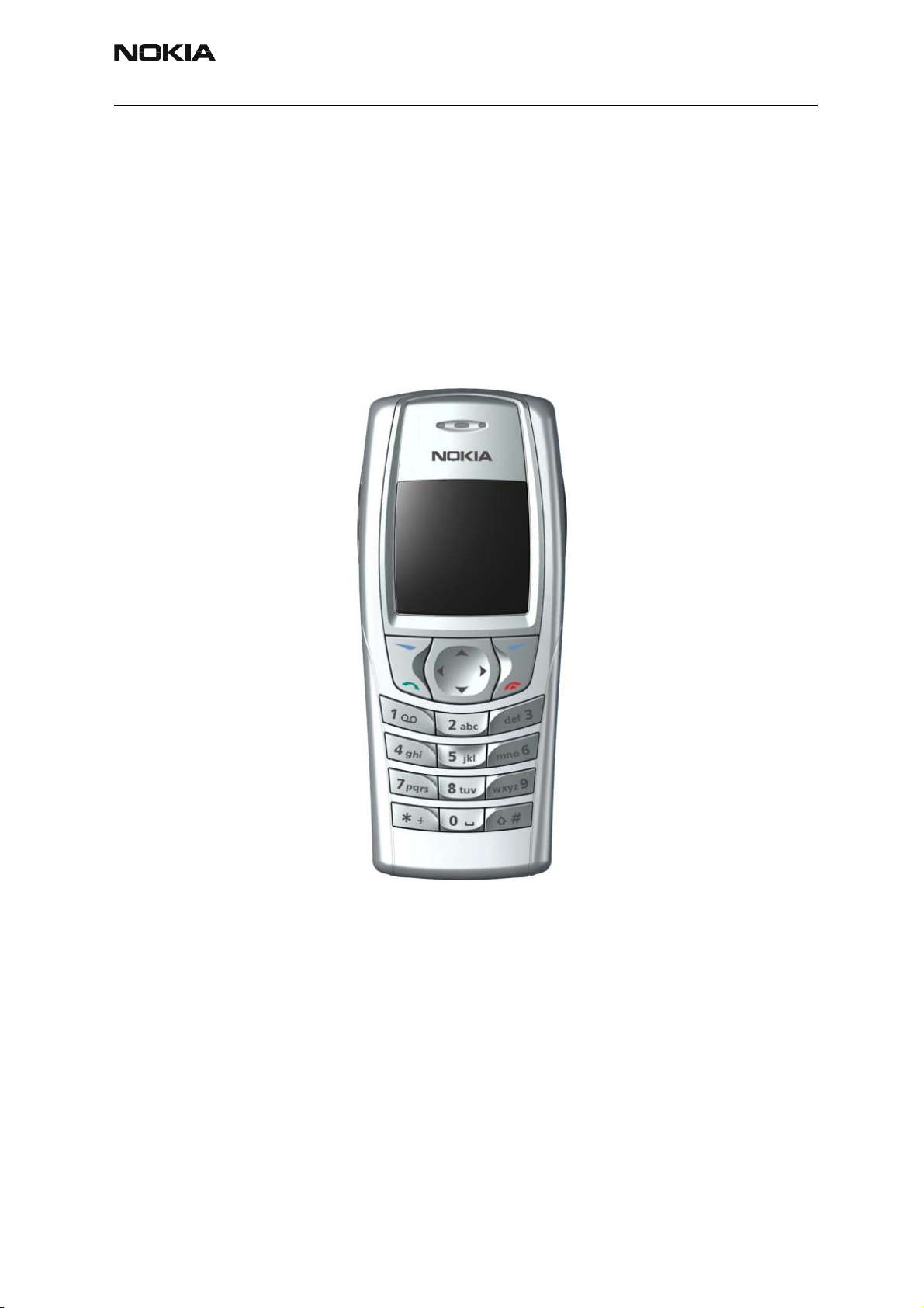
Model 6585
(RH-34 Series) Cellular Phones
Issue 1 Copyright © 2003 Nokia Corporation. All Rights Reserved
Page 2

Customer Care Solutions
Technical Documentation
Amendment Record Sheet
Amendment No Date Inserted By Comments
11/2003 J Fraser Issue 1
Issue 1 Copyright © 2003 Nokia Corporation. All Rights Reserved
Page 3

Customer Care Solutions
Technical Documentation
RH-34 (6585) Cellular Phones
Service Manual – Overall Manual Contents
Service Manual comprising
RH-34 Series Transceiver booklet comprising
Foreword
General
Parts
Service Software Instructions
Service Tools
Disassembly/Assembly
Troubleshooting - Antennas
Troubleshooting - Baseband
Troubleshooting - FM Radio
Troubleshooting - GPS
Troubleshooting - RF (Part 1 and Part 2)
System Module
Schematics
Issue 1 Copyright © 2003 Nokia Corporation. All Rights Reserved
Page 4

This document is intended for use by qualified service personnel only.
Company Policy
Our policy is of continuous development; details of all technical modifications will be
included with service bulletins.
While every endeavour has been made to ensure the accuracy of this document, some
errors may exist. If any errors are found by the reader, NOKIA Corporation should be
notified in writing.
Please state:
Customer Care Solutions
Technical Documentation
IMPORTANT
Title of the Document + Issue Number/Date of publication
Latest Amendment Number (if applicable)
Page(s) and/or Figure(s) in error
Please send to: Nokia Corporation
CCS Technical Documentation
PO Box 86
FIN-24101 SALO
Finland
Issue 1 Copyright © 2003 Nokia Corporation. All Rights Reserved
Page 5

Customer Care Solutions
Technical Documentation
Warnings and Cautions
Please refer to the phone's user guide for instructions relating to operation, care and
maintenance including important safety information. Note also the following:
Warnings:
1. CARE MUST BE TAKEN ON INSTALLATION IN VEHICLES FITTED WITH
ELECTRONIC ENGINE MANAGEMENT SYSTEMS AND ANTI-SKID BRAKING
SYSTEMS. UNDER CERTAIN FAULT CONDITIONS, EMITTED RF ENERGY CAN
AFFECT THEIR OPERATION. IF NECESSARY, CONSULT THE VEHICLE DEALER/
MANUFACTURER TO DETERMINE THE IMMUNITY OF VEHICLE ELECTRONIC
SYSTEMS TO RF ENERGY.
2. THE HANDPORTABLE TELEPHONE MUST NOT BE OPERATED IN AREAS LIKELY
TO CONTAIN POTENTIALLY EXPLOSIVE ATMOSPHERES EG PETROL STATIONS
(SERVICE STATIONS), BLASTING AREAS ETC.
3. OPERATION OF ANY RADIO TRANSMITTING EQUIPMENT, INCLUDING
Cautions:
1. Servicing and alignment must be undertaken by qualified personnel only.
2. Ensure all work is carried out at an anti-static workstation and that an
3. Ensure solder, wire, or foreign matter does not enter the telephone as
4. Use only approved components as specified in the parts list.
5. Ensure all components, modules screws and insulators are correctly
CELLULAR TELEPHONES, MAY INTERFERE WITH THE FUNCTIONALITY OF
INADEQUATELY PROTECTED MEDICAL DEVICES. CONSULT A PHYSICIAN OR
THE MANUFACTURER OF THE MEDICAL DEVICE IF YOU HAVE ANY
QUESTIONS. OTHER ELECTRONIC EQUIPMENT MAY ALSO BE SUBJECT TO
INTERFERENCE.
anti-static wrist strap is worn.
damage may result.
re-fitted after servicing and alignment. Ensure all cables and wires are
repositioned correctly.
Issue 1 Copyright © 2003 Nokia Corporation. All Rights Reserved
Page 6

CCS Technical Documentation
RH-34 Series Transceivers
General Information
Issue 1 11/2003 Confidential ©2003 Nokia Corporation
Page 7

RH-34
General Information CCS Technical Documentation
Contents
Page No
Handportables ................................................................................................................ 3
Sales Package ...............................................................................................................4
Module List ..................................................................................................................4
Technical Specifications ..............................................................................................4
General Specifications of Transceiver RH-34 .......................................................... 4
Supported Accessories .............................................................................................. 5
Page 2 ©2003 Nokia Corporation Confidential Issue 1 11/2003
Page 8
RH-34
CCS Technical Documentation General Information
Handportables
The Nokia 6585 (RH-34) offers a CDMA trimode (1900/800 MHz CDMA plus 800 AMPS
engine supporting 1XRTT. The RH-27 features an integrated FM radio, high-speed data
support, IR support, and RUIM.
RH-34 contains a 128 x 128 color display and has changeable display fonts. There is an
internal antenna, GPS (E-911) support, MIDI ringing tones, and an internal vibra.
Issue 1 11/2003 Confidential ©2003 Nokia Corporation Page 3
Page 9
RH-34
General Information CCS Technical Documentation
Sales Package
Module List
Name
Transceiver RH-34 Customer-
Battery (780 mAh Li-Ion) BLD-3 0670352
Rapid Performance Charger (US plug) ACP-12U 0675303
Type
Code
Material
Code
speciic
RH-34 (Nokia 6585)
A-cover assy 9458989
Keymat 9792498
Screws 6290107
Display 9517289
PWB assy 0202094
C-cover module 9491335
Battery 0670352
Technical Specifications
General Specifications of Transceiver RH-34
Parameter Specifications
Cellular system CDMA/AMPS, IS-19C, IS-98
IS-2000
TX frequency band 824.04 ... 848.97 MHz 1850 ... 1910 MHz
RX frequency band 869.04 ... 893.91 MHz 1930 ... 1990 MHz
Number of RF channels 832 1200
Channel spacing 30 kHz 50 kHz
Power levels -50dBm to +25dBm CDMA,
+8dBm to +26dBm AMPS
PCS J-STD-018, J-STD-008,
IS2000
-50dBm to +23dBm
Page 4 ©2003 Nokia Corporation Confidential Issue 1 11/2003
Page 10
RH-34
CCS Technical Documentation General Information
Parameter Mode Value and unit
Talk time Analog up to 50min.
Talk time Digital up to 2.4 hours
Standby time Analog up to 20 hours
Standby time Digital up to 10 days
Dimensions:
length
width
Weight 86.7 g - 3.1 ounces
105.8 mm - 4.17 inches
44.8 mm - 1.77 inches
Supported Accessories
Type Name Code
BLD-3 Standard 780 mAh Li-ion Battery 0670352
ACP-7U AC Travel Charger (US) 108-132 Vac 0675143
ACP-8U AC Charger 0675196
ACP-12U Rapid Performance Charger (US) 0675303
DDC-1 Spare Battery Charger 0675243
DCV-15 Desk stand with one-button synchronization 0675326
CARK-143 Advanced car kit 0080686
BHF-1 Headrest handsfree 0273278
LPS-4 Loopset 0630443
LCH-12 Cigarette Lighter Charger 0675328
HDB-4 Boom Headset 0694094
HS-5 Earbud Headset 0694121
HDS-3 FM Stereo Headset 0694093
HS-3 Fashion Stereo Headset 0694156
HS-10 Retractable Headset 0694126
DKU-5 USB cable 0273870
Issue 1 11/2003 Confidential ©2003 Nokia Corporation Page 5
Page 11

RH-34
General Information CCS Technical Documentation
Page 6 ©2003 Nokia Corporation Confidential Issue 1 11/2003
Page 12

CCS Technical Documentation
RH-34 Series Transceivers
Parts Lists
Issue 1 Amendment 12/2003 Confidential ©2003 Nokia Corporation
Page 13
RH-34
Parts Lists CCS Technical Documentation
Contents
Page No
Exploded View............................................................................................................... 3
Assembly Parts of Basic Transceiver RH-34 ..............................................................4
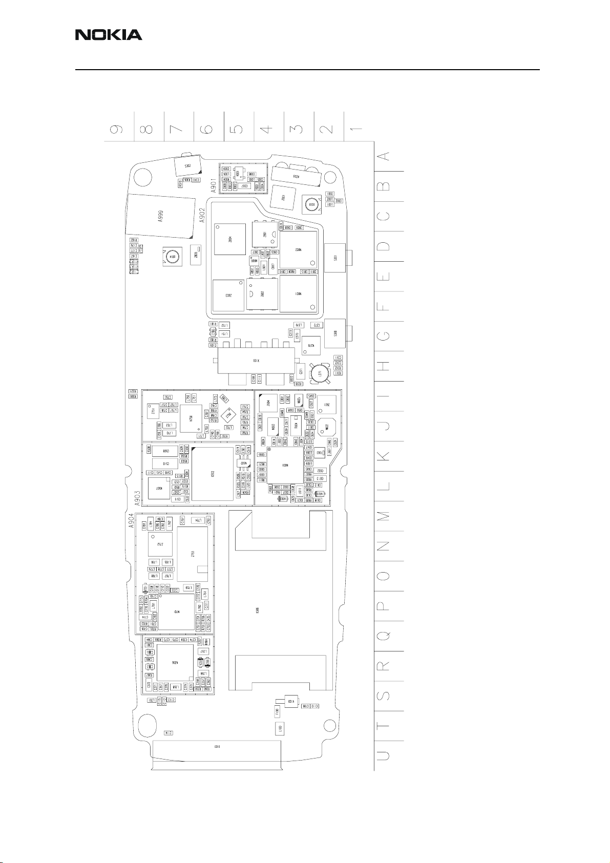
Component Layout — Top ..........................................................................................6
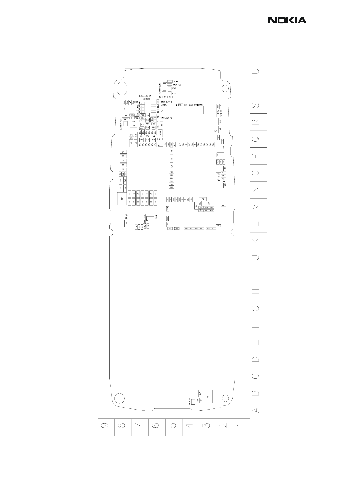
Component Layout — Bottom ....................................................................................7
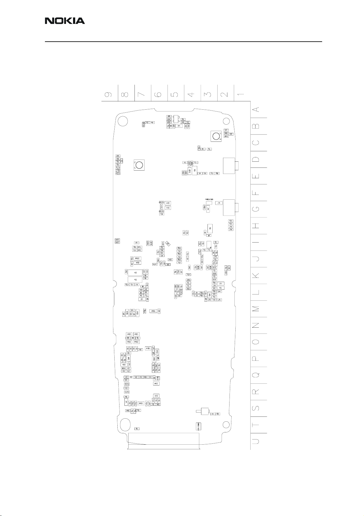
Component Values — Top .........................................................................................8
Component Values — Bottom .....................................................................................9
Parts List ...................................................................................................................... 10
RH-34 (6585) — EDMS Issue 9.4 Code: 0202124 ...................................................10
Page 2 ©2003 Nokia Corporation Confidential Issue 1 Amendment 12/2003
Page 14
RH-34
CCS Technical Documentation Parts Lists
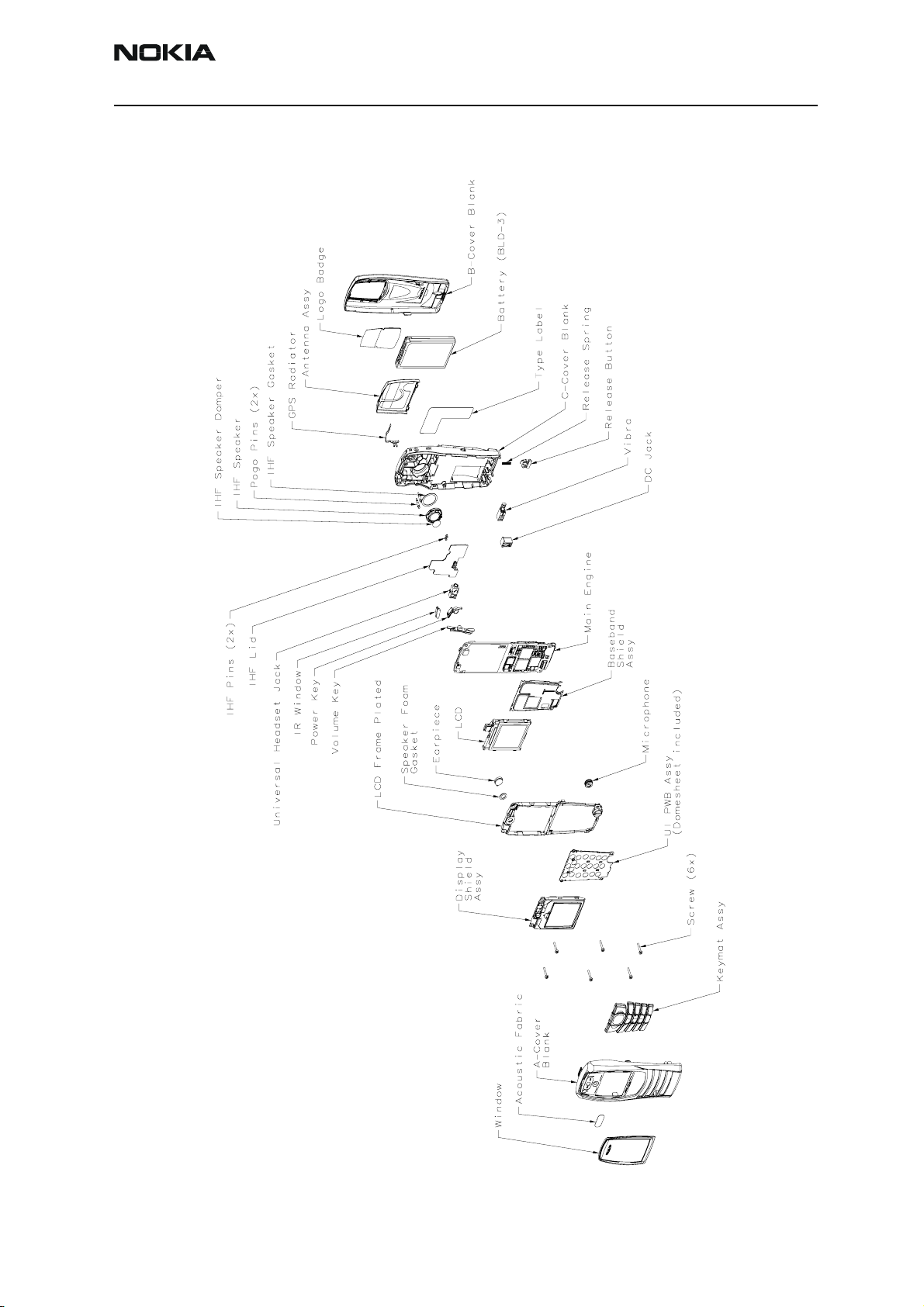
Exploded View
Issue 1 Amendment 12/2003 Confidential ©2003 Nokia Corporation Page 3
Page 15
RH-34
Parts Lists CCS Technical Documentation
Assembly Parts of Basic Transceiver RH-34
Item Qty Code
Window 1 9459246
9459247
9459248
Acoustic Fabric 1 9481098
A-Cover Blank 1 9453332
Keymat Assy 1 9791255
9791244
9791245
Screws 6 6290107
Display Shield Assy 1 9517370
UI PWB Assy (domesheet included) 1 0202222
LCD Frame plated 1 9467121
Speaker foam gasket 1 9481158
Microphone 1 5140263
LCD 1 4850291
Baseband shield assembly 1 9517329
Main engine 1 0202094
Volume key 1 9453377
Power key 1 9453133
IR window 1 9453137
Universal headset jack 1 5469801
IHF lid 1 9460573
IHF pins 2 9560164
DC jack 1 5400243
Vibra 1 6800057
Release button 1 9452502
Release spring 1 9511021
C-Cover blank 1 9453143
IHF speaker damper 1 9480909
IHF speaker 1 5140253
Pogo pins 2 5400319
IHF speaker gasket 1 9481118
GPS radiator 1 9560309
Page 4 ©2003 Nokia Corporation Confidential Issue 1 Amendment 12/2003
Page 16
RH-34
CCS Technical Documentation Parts Lists
Item Qty Code
Antenna Assy 1 0660301
Battery (BLD-3) 1 0670352
Logo badge 1 9430474
B-Cover 1 9453142
Issue 1 Amendment 12/2003 Confidential ©2003 Nokia Corporation Page 5
Page 17
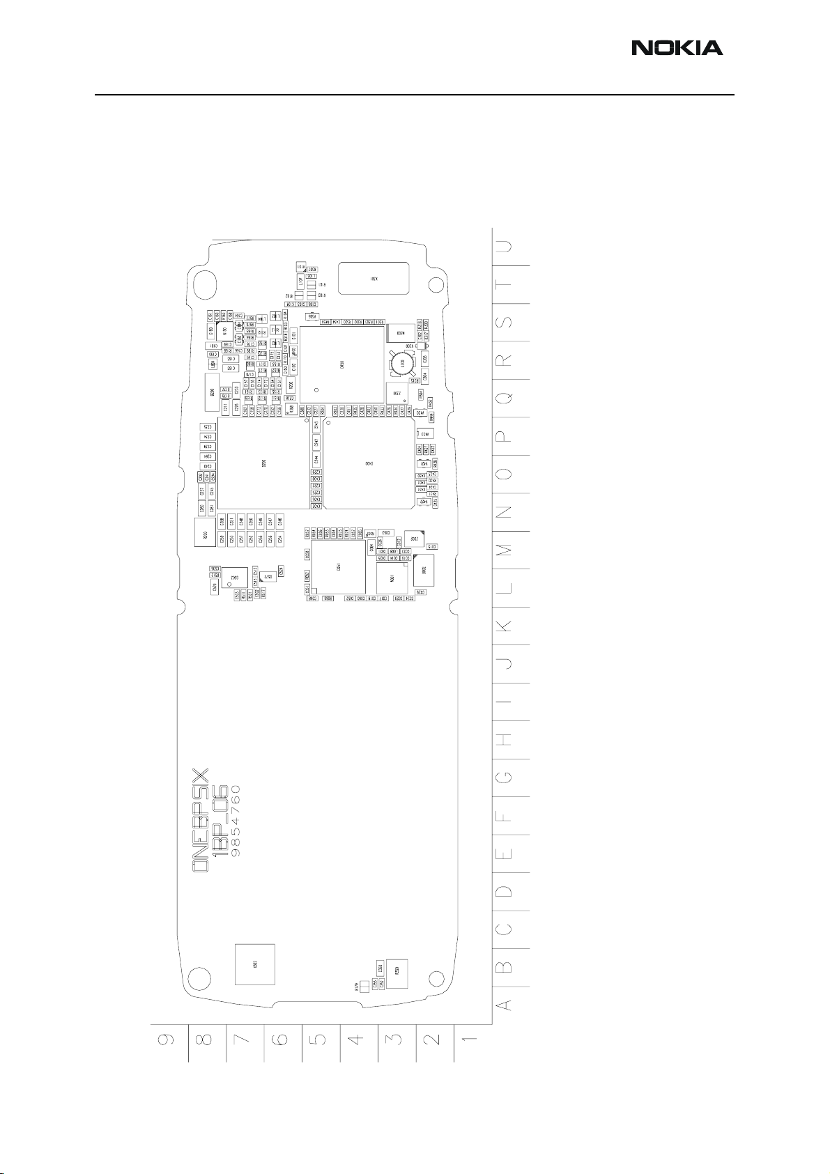
RH-34
Parts Lists CCS Technical Documentation
Component Layout — Top
Page 6 ©2003 Nokia Corporation Confidential Issue 1 Amendment 12/2003
Page 18
RH-34
CCS Technical Documentation Parts Lists
Component Layout — Bottom
Issue 1 Amendment 12/2003 Confidential ©2003 Nokia Corporation Page 7
Page 19
RH-34
Parts Lists CCS Technical Documentation
Component Values — Top
Page 8 ©2003 Nokia Corporation Confidential Issue 1 Amendment 12/2003
Page 20
RH-34
CCS Technical Documentation Parts Lists
Component Values — Bottom
Issue 1 Amendment 12/2003 Confidential ©2003 Nokia Corporation Page 9
Page 21
RH-34
Parts Lists CCS Technical Documentation
Parts List
RH-34 (6585) — EDMS Issue 9.4 Code: 0202124
Item Code Side X Y Description Value Type
R001 1430788 Bottom B 4 chip res 0W06 22K J 0402
R002 1430728 Bottom B 5 chip res 0W06 120R J 0402
R003 1430700 Bottom B 5 chip res 0W06 10R J 0402
R004 1430730 Bottom B 5 chip res 0W06 150R J 0402
R052 1430804 Top L 5 chip res 0W06 100K J 0402
R053 1430690 Top M 5 chip res jumper 0R0 0402
R054 1430690 Top M 5 chip res jumper 0R0 0402
R057 1430690 Top M 5 chip res jumper 0R0 0402
R060 1430690 Top L 5 chip res jumper 0R0 0402
R073 1430690 Top M 5 chip res jumper 0R0 0402
R074 1430690 Top M 4 chip res jumper 0R0 0402
R100 1620027 Top T 5 res network 0W06 2X47R J 0404
R101 1620027 Top T 5 res network 0W06 2X47R J 0404
R102 1620027 Top T 6 res network 0W06 2X47R J 0404
R103 1430804 Top S 6 chip res 0W06 100K J 0402
R104 1430812 Top S 6 chip res 0W06 220K J 0402
R110 1430804 Top R 6 chip res 0W06 100K J 0402
R112 1825031 Top S 7 varistor array 2XVWM16V VC50 0405
R113 1825031 Top S 6 varistor array 2XVWM16V VC50 0405
R150 1620031 Top R 7 res network 0W06 2X1K0 J 0404
R151 1620031 Top Q 6 res network 0W06 2X1K0 J 0404
R152 1620031 Top R 6 res network 0W06 2X1K0 J 0404
R153 1430778 Top R 6 chip res 0W06 10K J 0402
R155 1430796 Top Q 6 chip res 0W06 47K J 0402
R159 1620031 Top Q 7 res network 0W06 2X1K0 J 0404
R160 1620031 Top R 7 res network 0W06 2X1K0 J 0404
R161 1430796 Top Q 7 chip res 0W06 47K J 0402
R162 1430766 Bottom D 9 chip res 0W06 3K9 J 0402
R163 1430764 Top S 8 chip res 0W06 3K3 J 0402
Page 10 ©2003 Nokia Corporation Confidential Issue 1 Amendment 12/2003
Page 22

RH-34
CCS Technical Documentation Parts Lists
Item Code Side X Y Description Value Type
R164 1430700 Top S 7 chip res 0W06 10R J 0402
R165 1430700 Top S 7 chip res 0W06 10R J 0402
R166 1430700 Top R 7 chip res 0W06 10R J 0402
R169 1430762 Top R 7 chip res 0W06 2K2 J 0402
R170 1620031 Top R 7 res network 0W06 2X1K0 J 0404
R171 1620031 Top R 7 res network 0W06 2X1K0 J 0404
R172 1620031 Top Q 7 res network 0W06 2X1K0 J 0404
R173 1430875 Top Q 7 chip res 0W06 47K D 50PPM 0402
R177 1430693 Top Q 8 chip res 0W06 5R6 J 0402
R178 1430693 Top Q 8 chip res 0W06 5R6 J 0402
R179 1825031 Top A 4 varistor array 2XVWM16V VC50 0405
R180 1825033 Bottom G 6 chip varistor VWM14V VC46V 0402
R181 1825033 Bottom G 6 chip varistor VWM14V VC46V 0402
R183 1430770 Bottom E 9 chip res 0W06 4K7 J 0402
R185 1430690 Bottom D 8 chip res jumper 0R0 0402
R200 1419003 Top M 8 chip res 0W5 0R22 J 200PPM 1210
R202 1620043 Top Q 6 res network 0W03 4X100K J 0804
R203 1430770 Top Q 5 chip res 0W06 4K7 J 0402
R204 1430770 Top Q 5 chip res 0W06 4K7 J 0402
R220 1430690 Bottom I 3 chip res jumper 0R0 0402
R222 1430690 Bottom H 3 chip res jumper 0R0 0402
R300 1430788 Top S 2 chip res 0W06 22K J 0402
R301 1430742 Top S 3 chip res 0W06 390R J 0402
R302 1430742 Top S 4 chip res 0W06 390R J 0402
R304 1430690 Top Q 2 chip res jumper 0R0 0402
R306 1430770 Bottom B 7 chip res 0W06 4K7 J 0402
R307 1825033 Top T 5 chip varistor VWM14V VC46V 0402
R309 1430740 Bottom I 9 chip res 0W06 330R J 0402
R310 1825033 Bottom B 7 chip varistor VWM14V VC46V 0402
R311 1430770 Bottom H 2 chip res 0W06 4K7 J 0402
R312 1430770 Bottom H 2 chip res 0W06 4K7 J 0402
R315 1430691 Top Q 3 chip res 0W06 2R2 J 0402
Issue 1 Amendment 12/2003 Confidential ©2003 Nokia Corporation Page 11
Page 23
RH-34
Parts Lists CCS Technical Documentation
Item Code Side X Y Description Value Type
R316 1430816 Top S 2 chip res 0W06 330K J 0402
R317 1430784 Top S 2 chip res 0W06 15K J 0402
R318 1430726 Top S 6 chip res 0W06 100R J 0402
R320 1430742 Top S 4 chip res 0W06 390R J 0402
R321 1430740 Bottom I 9 chip res 0W06 330R J 0402
R350 1419009 Top B 3 chip res 0W5 4R7 J 220PPM 1210
R357 1430792 Bottom Q 6 chip res 0W06 33K J 0402
R359 1430778 Bottom S 6 chip res 0W06 10K J 0402
R360 1430804 Bottom S 6 chip res 0W06 100K J 0402
R361 1620019 Bottom Q 3 res network 0W06 2X10K J 0404
R367 1430786 Bottom R 8 chip res 0W06 18K J 0402
R369 1430792 Bottom Q 8 chip res 0W06 33K J 0402
R388 4120071 Top Q 6 ASIP EMIF03-SIM01
SIM Filter
R427 1430754 Top P 2 chip res 0W06 1K0 J 0402
R428 1430770 Top O 2 chip res 0W06 4k7 J 0402
R430 1430754 Top O 2 chip res 0W06 1K0 J 0402
R431 1430770 Top N 2 chip res 0W06 4K7 J 0402
R432 1430796 Top Q 2 chip res 0W06 47K J 0402
R433 1430754 Top Q 2 chip res 0W06 1K0 J 0402
R434 1430770 Top Q 3 chip res 0W06 4K7 J 0402
R435 1430770 Top Q 4 chip res 0W06 4K7 J 0402
R450 1430770 Top S 5 chip res 0W06 4K7 J 0402
R501 1430700 Bottom L 7 chip res 0W06 10R J 0402
R503 1430778 Bottom K 7 chip res 0W06 10K J 0402
R505 1430700 Bottom L 5 chip res 0W06 10R J 0402
BGA8
R506 1430706 Bottom L 5 chip res 0W06 15R J 0402
R508 1430766 Bottom K 8 chip res 0W06 3K9 J 0402
R509 1430726 Bottom L 5 chip res 0W06 100R J 0402
R511 1430794 Top L 7 chip res 0W06 39K J 0402
R512 1430700 Top L 8 chip res 0W06 10R J 0402
R513 1430700 Bottom L 7 chip res 0W06 10R J 0402
R515 1430700 Bottom L 7 chip res 0W06 10R J 0402
Page 12 ©2003 Nokia Corporation Confidential Issue 1 Amendment 12/2003
Page 24
RH-34
CCS Technical Documentation Parts Lists
Item Code Side X Y Description Value Type
R517 1430784 Top L 7 chip res 0W06 15K J 0402
R519 1430726 Bottom L 5 chip res 0W06 100R J 0402
R521 1430774 Top L 7 chip res 0W06 6K8 J 0402
R550 1430778 Bottom K 7 chip res 0W06 10K J 0402
R601 1430758 Bottom L 4 chip res 0W06 1K5 J 0402
R602 1430790 Bottom L 4 chip res 0W06 27K J 0402
R604 1430772 Bottom K 4 chip res 0W06 5K6 J 0402
R605 1430754 Bottom L 3 chip res 0W06 1K0 J 0402
R606 1430754 Bottom L 3 chip res 0W06 1K0 J 0402
R607 1430770 Bottom L 3 chip res 0W06 4K7 J 0402
R609 1430758 Bottom L 3 chip res 0W06 1K5 J 0402
R611 1430804 Bottom L 4 chip res 0W06 100K J 0402
R621 1430774 Bottom K 4 chip res 0W06 6K8 J 0402
R701 1430762 Bottom Q 6 chip res 0W06 2K2 J 0402
R702 1430754 Bottom P 8 chip res 0W06 1K0 J 0402
R703 1430744 Bottom Q 8 chip res 0W06 470R J 0402
R704 1430770 Bottom P 8 chip res 0W06 4K7 J 0402
R705 1430790 Bottom Q 8 chip res 0W06 27K J 0402
R706 1430776 Bottom P 6 chip res 0W06 8K2 J 0402
R707 1430724 Bottom J 5 chip res 0W06 82R J 0402
R750 1430681 Bottom J 6 chip res 0W06 4R3 J 0402
R764 1430796 Bottom J 5 chip res 0W06 47K J 0402
R765 1430796 Bottom J 5 chip res 0W06 47K J 0402
R768 1430796 Bottom J 5 chip res 0W06 47K J 0402
R769 1430681 Bottom I 6 chip res 0W06 4R3 J 0402
R801 1430734 Bottom E 5 chip res 0W06 220R J 0402
R802 1430746 Bottom D 4 chip res 0W06 560R J 0402
R803 1430734 Bottom E 4 chip res 0W06 220R J 0402
R808 1820039 Bottom E 3 NTC RES 0W1 47K J
B=4050+-3%
R976 1430700 Top S 7 chip res 0W06 10R J 0402
R977 1430700 Top S 7 chip res 0W06 10R J 0402
R999 1430804 Top Q 2 chip res 0W06 100K J 0402
0402
Issue 1 Amendment 12/2003 Confidential ©2003 Nokia Corporation Page 13
Page 25

RH-34
Parts Lists CCS Technical Documentation
Item Code Side X Y Description Value Type
C001 2320518 Bottom B 2 chip cap NP0 1P8 C 50V 0402
C002 2320520 Bottom B 2 chip cap NP0 2P2 C 50V 0402
C004 2320805 Bottom B 4 chip cap X5R 100N K 10V 0402
C005 2320546 Bottom B 4 chip cap NP0 27P J 50V 0402
C006 2320536 Bottom B 5 chip cap NP0 10P J 50V 0402
C007 2320481 Bottom B 5 chip cap X5R 1U K 6V3 0603
C008 2320552 Bottom B 5 chip cap NP0 47P J 50V 0402
C009 2320532 Bottom A 5 chip cap NP0 6P8 C 50V 0402
C012 2320522 Top M 3 chip cap NP0 2P7 C 50V 0402
C014 2320540 Top M 3 chip cap NP0 15P J 50V 0402
C015 2320778 Top M 2 chip cap X7R 10N K 16V 0402
C017 2320544 Top L 3 chip cap NP0 22P J 50V 0402
C018 2320805 Top L 4 chip cap X5R 100N K 10V 0402
C019 2320620 Top M 3 chip cap X7R 10N J 16V 0402
C020 2320620 Top L 3 chip cap X7R 10N J 16V 0402
C021 2320620 Top M 3 chip cap X7R 10N J 16V 0402
C023 2320544 Top M 3 chip cap NP0 22P J 50V 0402
C024 2320544 Top L 3 chip cap NP0 22P J 50V 0402
C025 2320544 Top M 3 chip cap NP0 22P J 50V 0402
C026 2320805 Top M 3 chip cap X5R 100N K 10V 0402
C029 2320536 Top L 2 chip cap NP0 10P J 50V 0402
C051 2320805 Top L 5 chip cap X5R 100N K 10V 0402
C052 2320805 Top L 4 chip cap X5R 100N K 10V 0402
C054 2320805 Top M 5 chip cap X5R 100N K 10V 0402
C056 2320805 Top M 5 chip cap X5R 100N K 10V 0402
C057 2320805 Top M 4 chip cap X5R 100N K 10V 0402
C058 2320805 Top M 5 chip cap X5R 100N K 10V 0402
C060 2320805 Top L 4 chip cap X5R 100N K 10V 0402
C063 2316001 Top M 3 chip cap X5R 2U2 K 6V3 0603
C064 2316001 Top M 4 chip cap X5R 2U2 K 6V3 0603
C065 2320620 Top M 4 chip cap X7R 10N J 16V 0402
C068 2320778 Top L 5 chip cap X7R 10N K 16V 0402
Page 14 ©2003 Nokia Corporation Confidential Issue 1 Amendment 12/2003
Page 26

RH-34
CCS Technical Documentation Parts Lists
Item Code Side X Y Description Value Type
C101 2320481 Top S 6 chip cap X5R 1U K 6V3 0603
C102 2320481 Top R 6 chip cap X5R 1U K 6V3 0603
C103 2320544 Top S 6 chip cap NP0 22P J 50V 0402
C104 2320544 Top S 6 chip cap NP0 22P J 50V 0402
C105 2320544 Top S 5 chip cap NP0 22P J 50V 0402
C106 2320744 Bottom S 3 chip cap X7R 1N0 K 50V 0402
C107 2320778 Top R 6 chip cap X7R 10N K 16V 0402
C108 2320552 Bottom H 5 chip cap NP0 47P J 50V 0402
C109 2320552 Bottom G 6 chip cap NP0 47P J 50V 0402
C110 2320544 Bottom S 2 chip cap NP0 22P J 50V 0402
C111 2320552 Bottom H 4 chip cap NP0 47P J 50V 0402
C112 2320536 Bottom S 7 chip cap NP0 10P J 50V 0402
C113 2320536 Bottom S 7 chip cap NP0 10P J 50V 0402
C114 2320536 Bottom T 7 chip cap NP0 10P J 50V 0402
C115 2320536 Bottom S 8 chip cap NP0 10P J 50V 0402
C150 2320805 Top R 6 chip cap X5R 100N K 10V 0402
C151 2320805 Top Q 6 chip cap X5R 100N K 10V 0402
C152 2320552 Top R 6 chip cap NP0 47P J 50V 0402
C153 2320552 Top R 6 chip cap NP0 47P J 50V 0402
C154 2320805 Top Q 6 chip cap X5R 100N K 10V 0402
C155 2320805 Top Q 7 chip cap X5R 100N K 10V 0402
C156 2320552 Top Q 6 chip cap NP0 47P J 50V 0402
C157 2320805 Top Q 7 chip cap X5R 100N K 10V 0402
C158 2320552 Top Q 7 chip cap NP0 47P J 50V 0402
C159 2320552 Top R 7 chip cap NP0 47P J 50V 0402
C160 2320805 Top S 8 chip cap X5R 100N K 10V 0402
C161 2320805 Top S 8 chip cap X5R 100N K 10V 0402
C162 2320552 Top Q 7 chip cap NP0 47P J 50V 0402
C163 2320505 Top R 7 chip cap X5R 4U7 K 6.3V 0603
C164 2320805 Top S 7 chip cap X5R 100N K 10V 0402
C165 2320505 Top R 7 chip cap X5R 4U7 K 6.3V 0603
C166 2320805 Top R 7 chip cap X5R 100N K 10V 0402
Issue 1 Amendment 12/2003 Confidential ©2003 Nokia Corporation Page 15
Page 27
RH-34
Parts Lists CCS Technical Documentation
Item Code Side X Y Description Value Type
C167 2320552 Bottom D 9 chip cap NP0 47P J 50V 0402
C168 2320805 Top S 7 chip cap X5R 100N K 10V 0402
C169 2320805 Top R 7 chip cap X5R 100N K 10V 0402
C170 2320552 Top Q 6 chip cap NP0 47P J 50V 0402
C171 2320552 Top R 7 chip cap NP0 47P J 50V 0402
C172 2320805 Top Q 6 chip cap X5R 100N K 10V 0402
C173 2320552 Top Q 7 chip cap NP0 47P J 50V 0402
C174 2320805 Top Q 7 chip cap X5R 100N K 10V 0402
C175 2320805 Top R 6 chip cap X5R 100N K 10V 0402
C176 2320805 Top R 7 chip cap X5R 100N K 10V 0402
C177 2320552 Bottom D 9 chip cap NP0 47P J 50V 0402
C179 2320805 Bottom D 9 chip cap X5R 100N K 10V 0402
C180 2320481 Top S 8 chip cap X5R 1U K 6V3 0603
C181 2320481 Top R 8 chip cap X5R 1U K 6V3 0603
C182 2320805 Bottom E 9 chip cap X5R 100N K 10V 0402
C183 2315201 Top S 7 chip array NP0 2X27P K 25V 0405
C184 2315201 Top S 7 chip array NP0 2X27P K 25V 0405
C185 2315205 Bottom G 6 chip array X5R 2X1N M 16V 0405
C190 2320548 Top R 8 chip cap NP0 33P J 50V 0402
C202 2320778 Top O 8 chip cap X7R 10N K 16V 0402
C211 2320481 Top Q 8 chip cap X5R 1U K 6V3 0603
C222 2320805 Top O 5 chip cap X5R 100N K 10V 0402
C224 2320143 Top O 8 chip cap X5R 220N K 6.3V 0402
C225 2320805 Top O 5 chip cap X5R 100N K 10V 0402
C226 2320481 Top Q 7 chip cap X5R 1U K 6V3 0603
C227 2320778 Top Q 5 chip cap X7R 10N K 16V 0402
C229 2320805 Top O 5 chip cap X5R 100N K 10V 0402
C230 2320778 Top Q 4 chip cap X7R 10N K 16V 0402
C232 2320778 Top Q 5 chip cap X7R 10N K 16V 0402
C233 2320481 Top Q 7 chip cap X5R 1U K 6V3 0603
C234 2320481 Top P 8 chip cap X5R 1U K 6V3 0603
C235 2320481 Top P 8 chip cap X5R 1U K 6V3 0603
Page 16 ©2003 Nokia Corporation Confidential Issue 1 Amendment 12/2003
Page 28
RH-34
CCS Technical Documentation Parts Lists
Item Code Side X Y Description Value Type
C237 2320481 Top O 8 chip cap X5R 1U K 6V3 0603
C238 2320805 Top Q 6 chip cap X5R 100N K 10V 0402
C239 2320481 Top P 8 chip cap X5R 1U K 6V3 0603
C240 2320481 Top O 8 chip cap X5R 1U K 6V3 0603
C241 2320805 Top O 8 chip cap X5R 100N K 10V 0402
C242 2320481 Top P 5 chip cap X5R 1U K 6V3 0603
C243 2320481 Top P 5 chip cap X5R 1U K 6V3 0603
C244 2320481 Top O 5 chip cap X5R 1U K 6V3 0603
C245 2320481 Top O 8 chip cap X5R 1U K 6V3 0603
C246 2320481 Top N 6 chip cap X5R 1U K 6V3 0603
C247 2320481 Top N 6 chip cap X5R 1U K 6V3 0603
C248 2320481 Top N 7 chip cap X5R 1U K 6V3 0603
C249 2320481 Top N 7 chip cap X5R 1U K 6V3 0603
C250 2320481 Top N 7 chip cap X5R 1U K 6V3 0603
C251 2320481 Top N 7 chip cap X5R 1U K 6V3 0603
C252 2320481 Top M 7 chip cap X5R 1U K 6V3 0603
C253 2320481 Top M 7 chip cap X5R 1U K 6V3 0603
C254 2320481 Top M 6 chip cap X5R 1U K 6V3 0603
C255 2320481 Top M 7 chip cap X5R 1U K 6V3 0603
C256 2320481 Top M 6 chip cap X5R 1U K 6V3 0603
C257 2320481 Top M 7 chip cap X5R 1U K 6V3 0603
C258 2320481 Top N 8 chip cap X5R 1U K 6V3 0603
C259 2320481 Top M 8 chip cap X5R 1U K 6V3 0603
C260 2320505 Top N 8 chip cap X5R 4U7 K 6.3V 0603
C261 2320505 Top N 8 chip cap X5R 4U7 K 6.3V 0603
C264 2320481 Top O 8 chip cap XR5 1U K 6V3 0603
C270 2320505 Bottom G 3 chip cap X5R 4U7 K 6.3V 0603
C271 2310037 Bottom H 3 chip cap X5R 10U M 6V3 0805
C272 2320505 Bottom G 2 chip cap X5R 4U7 K 6.3V 0603
C273 2320805 Bottom G 3 chip cap X5R 100N K 10V 0402
C302 2320556 Top S 2 chip cap NP0 68P J 50V 0402
C303 2320125 Top R 2 chip cap X5R 1U K 16V 0603
Issue 1 Amendment 12/2003 Confidential ©2003 Nokia Corporation Page 17
Page 29

RH-34
Parts Lists CCS Technical Documentation
Item Code Side X Y Description Value Type
C304 2320125 Top R 2 chip cap X5R 1U K 16V 0603
C310 2320544 Bottom B 6 chip cap NP0 22P J 50V 0402
C311 2320544 Bottom H 2 chip cap NP0 22P J 50V 0402
C312 2320544 Bottom H 2 chip cap NP0 22P J 50V 0402
C350 2320505 Top B 3 chip cap X5R 4U7 K 6.3V 0603
C352 2320805 Top B 3 chip cap X5R 100N K 10V 0402
C353 2320805 Top B 4 chip cap X5R 100N K 10V 0402
C357 2320778 Bottom S 6 chip cap X7R 10N K 16V 0402
C358 2320785 Bottom S 6 chip cap X7R 47N K 10V 0402
C359 2320805 Bottom Q 7 chip cap X5R 100N K 10V 0402
C361 2320744 Bottom Q 8 chip cap X7R 1N0 K 50V 0402
C362 2320778 Bottom S 6 chip cap X7R 10N K 16V 0402
C363 2315261 Bottom R 8 chip array X5R 2X47N K 10V 0405
C364 2321007 Bottom Q 8 chip cap X7R 22N K 16V 0402
C365 2315209 Bottom R 8 chip array X5R 2X33N M 10V 0405
C366 2320785 Bottom R 8 chip cap X7R 47N K 10V 0402
C367 2320560 Bottom S 8 chip cap NP0 100P J 50V 0402
C370 2320760 Bottom S 7 chip cap X7R 4N7 K 25V 0402
C371 2320778 Bottom S 8 chip cap X7R 10N K 16V 0402
C372 2320481 Bottom S 8 chip cap X5R 1U K 6V3 0603
C373 2321007 Bottom Q 7 chip cap X7R 22N K 16V 0402
C374 2320744 Bottom Q 7 chip cap X7R 1N0 K 50V 0402
C375 2320752 Bottom Q 7 chip cap X7R 2N2 K 50V 0402
C378 2320546 Bottom S 7 chip cap NP0 27P J 50V 0402
C379 2320552 Bottom S 7 chip cap NP0 47P J 50V 0402
C388 2320805 Top Q 6 chip cap X5R 100N K 10V 0402
C400 2320805 Top O 5 chip cap X5R 100N K 10V 0402
C401 2320805 Top O 2 chip cap X5R 100N K 10V 0402
C402 2320805 Top N 5 chip cap X5R 100N K 10V 0402
C403 2320805 Top Q 4 chip cap X5R 100N K 10V 0402
C404 2320805 Top P 2 chip cap X5R 100N K 10V 0402
C405 2320805 Top N 5 chip cap X5R 100N K 10V 0402
Page 18 ©2003 Nokia Corporation Confidential Issue 1 Amendment 12/2003
Page 30

RH-34
CCS Technical Documentation Parts Lists
Item Code Side X Y Description Value Type
C422 2320620 Top P 2 chip cap X7R 10N J 16V 0402
C423 2320744 Top O 2 chip cap X7R 1N0 K 50V 0402
C424 2320620 Top O 2 chip cap X7R 10N J 16V 0402
C425 2320744 Top N 2 chip cap X7R 1N0 K 50V 0402
C426 2320620 Top Q 3 chip cap X7R 10N J 16V 0402
C427 2320744 Top Q 3 chip cap X7R 1N0 K 50V 0402
C428 2320778 Top Q 4 chip cap X7R 10N K 16V 0402
C429 2320783 Top Q 3 chip cap X7R 33N K 10V 0402
C430 2320783 Top O 2 chip cap X7R 33N K 10V 0402
C431 2320783 Top O 2 chip cap X7R 33N K 10V 0402
C435 2320778 Bottom P 6 chip cap X7R 10N K 16V 0402
C450 2320778 Top Q 4 chip cap X7R 10N K 16V 0402
C451 2320805 Top Q 4 chip cap X5R 100N K 10V 0402
C454 2320778 Top S 5 chip cap X7R 10N K 16V 0402
C501 2320552 Bottom L 7 chip cap NP0 47P J 50V 0402
C502 2320576 Top L 7 chip cap X7R 470P J 50V 0402
C503 2320783 Top L 7 chip cap X7R 33N K 10V 0402
C504 2320620 Bottom L 7 chip cap X7R 10N J 16V 0402
C505 2320620 Top M 8 chip cap X7R 10N J 16V 0402
C507 2320620 Bottom L 7 chip cap X7R 10N J 16V 0402
C508 2420003 Bottom K 7 chip cap PPS 33N J 16V 1206
C509 2320584 Bottom K 7 chip cap X7R 1N0 J 50 V 0402
C510 2420003 Bottom K 7 chip cap PPS 33N J 16V 1206
C511 2320481 Bottom L 7 chip cap X5R 1U K 6V3 0603
C512 2320576 Top L 7 chip cap X7R 470P J 50V 0402
C513 2320576 Top L 7 chip cap X7R 470P J 50V 0402
C514 2320550 Bottom K 5 chip cap NP0 39P J 50V 0402
C515 2320552 Bottom L 8 chip cap NP0 47P J 50V 0402
C516 2320548 Bottom L 5 chip cap NP0 33P J 50V 0402
C517 2320576 Bottom L 8 chip cap X7R 470P J 50V 0402
C518 2320618 Bottom L 7 chip cap X7R 4N7 J 25V 0402
C519 2320522 Bottom K 5 chip cap NP0 2P7 C 50V 0402
Issue 1 Amendment 12/2003 Confidential ©2003 Nokia Corporation Page 19
Page 31

RH-34
Parts Lists CCS Technical Documentation
Item Code Side X Y Description Value Type
C520 2320481 Top L 8 chip cap X5R 1U K 6V3 0603
C521 2320805 Bottom L 7 chip cap X5R 100N K 10V 0402
C522 2320620 Bottom L 7 chip cap X7R 10N J 16V 0402
C524 2320546 Top L 6 chip cap NP0 27P J 50V 0402
C532 2320532 Bottom L 7 chip cap NP0 6P8 C 50V 0402
C550 2320584 Bottom K 7 chip cap X7R 1N0 J 50V 0402
C553 2320538 Bottom L 5 chip cap NP0 12P J 50V 0402
C602 2320633 Bottom L 3 chip cap NP0 220P J 25V 0402
C603 2320538 Bottom K 4 chip cap NP0 12P J 50V 0402
C605 2320560 Bottom K 3 chip cap NP0 100P J 50V 0402
C606 2320744 Bottom L 4 chip cap X7R 1N0 K 50V 0402
C607 2320620 Bottom L 4 chip cap X7R 10N J 16V 0402
C608 2320538 Bottom I 3 chip cap NP0 12P J 50V 0402
C611 2320538 Bottom J 3 chip cap NP0 12P J 50V 0402
C612 2320584 Bottom L 2 chip cap X7R 1N0 J 50V 0402
C613 2320109 Bottom L 2 chip cap X7R 15N J 25V 0603
C614 2320538 Bottom K 4 chip cap NP0 12P J 50V 0402
C618 2320602 Bottom L 2 chip cap NP0 4P7 C 50V 0402
C619 2320552 Bottom J 4 chip cap NP0 47P J 50V 0402
C621 2320744 Bottom J 4 chip cap X7R 1N0 K 50V 0402
C627 2320538 Bottom I 3 chip cap NP0 12P J 50V 0402
C629 2321011 Bottom L 3 chip cap NP0 8P0+/-0.5P 50V 0402
C630 2320604 Bottom L 3 chip cap NP0 18P J 50V 0402
C631 2320520 Bottom L 3 chip cap NP0 2P2 C 50V 0402
C632 2320560 Bottom L 3 chip cap NP0 100P J 50V 0402
C633 2320552 Bottom J 3 chip cap NP0 47P J 50V 0402
C634 2320596 Bottom K 2 chip cap X7R 3N3 J 50V 0402
C635 2320596 Bottom J 3 chip cap X7R 3N3 J 50V 0402
C637 2320560 Bottom L 3 chip cap NP0 100P J 50V 0402
C638 2320620 Bottom L 3 chip cap X7R 10N J 16V 0402
C639 2320596 Bottom J 3 chip cap X7R 3N3 J 50V 0402
C640 2320524 Bottom K 3 chip cap NP0 3P3 C 50V 0402
Page 20 ©2003 Nokia Corporation Confidential Issue 1 Amendment 12/2003
Page 32

RH-34
CCS Technical Documentation Parts Lists
Item Code Side X Y Description Value Type
C642 2320524 Bottom K 3 chip cap NP0 3P3 C 50V 0402
C645 2320538 Bottom I 3 chip cap NP0 12P J 50V 0402
C646 2320538 Bottom K 3 chip cap NP0 12P J 50V 0402
C647 2320538 Bottom K 3 chip cap NP0 12P J 50V 0402
C648 2320744 Bottom J 3 chip cap X7R 1N0 K 50V 0402
C649 2320522 Bottom J 4 chip cap NP0 47P J 50V 0402
C650 2320538 Bottom I 3 chip cap NP0 12P J 50V 0402
C651 2320538 Bottom J 3 chip cap NP0 12P J 50V 0402
C652 2320481 Bottom K 2 chip cap X5R 1U K 6V3 0603
C660 2320538 Bottom K 2 chip cap NP0 12P J 50V 0402
C666 2320552 Bottom K 4 chip cap NP0 47P J 50V 0402
C677 2320552 Bottom J 3 chip cap NP0 47P J 50V 0402
C701 2320783 Bottom Q 8 chip cap X7R 33N K 10V 0402
C702 2320584 Bottom P 8 chip cap X7R 1N0 J 50V 0402
C703 2320805 Bottom Q 6 chip cap X5R 100N K 10V 0402
C704 2320778 Bottom P 6 chip cap X7R 10N K 16V 0402
C706 2320778 Bottom Q 8 chip cap X7R 10N K 16V 0402
C707 2320778 Bottom Q 6 chip cap X7R 10N K 16V 0402
C708 2320778 Bottom O 8 chip cap X7R 10N K 16V 0402
C710 2320778 Bottom P 8 chip cap X7R 10N K 16V 0402
C712 2320778 Bottom O 8 chip cap X7R 10N K 16V 0402
C714 2360001 Bottom P 8 chip cap X5R 330N K 10V 0603
C715 2320620 Bottom P 8 chip cap X7R 10N J 16V 0402
C716 2320544 Bottom P 8 chip cap NP0 22P J 50V 0402
C718 2320778 Bottom O 8 chip cap X7R 10N K 16V 0402
C722 2320778 Bottom O 7 chip cap X7R 10N K 16V 0402
C723 2320778 Bottom O 7 chip cap X7R 10N K 16V 0402
C740 2320544 Bottom O 7 chip cap NP0 22P J 50V 0402
C750 2320560 Bottom J 5 chip cap NP0 100P J 50V 0402
C753 2320560 Bottom I 5 chip cap NP0 100P J 50V 0402
C755 2320516 Bottom I 7 chip cap NP0 1P5 C 50V 0402
C756 2320560 Bottom J 5 chip cap NP0 100P J 50V 0402
Issue 1 Amendment 12/2003 Confidential ©2003 Nokia Corporation Page 21
Page 33

RH-34
Parts Lists CCS Technical Documentation
Item Code Side X Y Description Value Type
C757 2320554 Bottom I 7 chip cap NP0 56P J 50V 0402
C758 2320785 Bottom I 7 chip cap X7R 47N K 10V 0402
C759 2320602 Bottom J 8 chip cap NP0 4P7 C 50V 0402
C761 2320596 Bottom M 6 chip cap X7R 3N3 J 50V 0402
C763 2320538 Bottom I 6 chip cap NP0 12P J 50V 0402
C766 2320560 Bottom J 8 chip cap NP0 100P J 50V 0402
C767 2320576 Bottom M 7 chip cap X7R 470P J 50V 0402
C769 2320596 Bottom J 6 chip cap X7R 3N3 J 50V 0402
C770 2320514 Bottom O 6 chip cap NP0 1P2 C 50V 0402
C771 2320532 Bottom P 6 chip cap NP0 6P8 C 50V 0402
C772 2320532 Bottom P 6 chip cap NP0 6P8 C 50V 0402
C777 2320536 Bottom O 7 chip cap NP0 10P J 50V 0402
C778 2320532 Bottom O 8 chip cap NP0 6P8 C 50V 0402
C779 2320532 Bottom O 8 chip cap NP0 6P8 C 50V 0402
C781 2320526 Bottom M 8 chip cap NP0 3P9 C 50V 0402
C783 2320602 Bottom M 8 chip cap NP0 4P7 C 50V 0402
C784 2320584 Bottom M 8 chip cap X7R 1N0 J 50V 0402
C785 2320516 Bottom I 5 chip cap NP0 1P5 C 50V 0402
C786 2320805 Bottom M 8 chip cap X5R 100N K 10V 0402
C787 2320538 Bottom J 6 chip cap NP0 12P J 50V 0402
C788 2320805 Bottom J 6 chip cap X5R 100N K 10V 0402
C801 2320552 Bottom I 4 chip cap NP0 47P J 50V 0402
C802 2320538 Bottom I 3 chip cap NP0 12P J 50V 0402
C803 2320538 Bottom D 4 chip cap NP0 12P J 50V 0402
C807 2320778 Bottom D 4 chip cap X7R 10N K 16V 0402
C808 2320584 Bottom C 3 chip cap X7R 1N0 J 50V 0402
C809 2320540 Bottom C 3 chip cap NP0 15P J 50V 0402
C810 2320584 Bottom E 4 chip cap X7R 1N0 J 50V 0402
C811 2320556 Bottom E 3 chip cap NP0 68P J 50V 0402
C813 2320552 Bottom E 3 chip cap NP0 47P J 50V 0402
C814 2320560 Bottom C 4 chip cap NP0 100P J 50V 0402
C817 2310037 Bottom E 4 chip cap X5R 10U M 6V3 0805
Page 22 ©2003 Nokia Corporation Confidential Issue 1 Amendment 12/2003
Page 34

RH-34
CCS Technical Documentation Parts Lists
Item Code Side X Y Description Value Type
L001 3646401 Bottom C 2 chip coil 2N J Q16/250MHz 0402
L002 3646009 Bottom B 2 chip coil 10N J Q30/800MHz 0402
L005 3646061 Bottom B 5 chip coil 15N J Q30/800MHz 0402
L006 3646051 Bottom B 5 chip coil 3N9+-0N3
Q28/800MHz
L008 3646055 Top M 3 chip coil 8N2 J Q28/800MHz 0402
L100 3203743 Bottom T 4 ferrite bead 0R03 42R/100MHz 3A 0805
L102 3203803 Top R 6 chip bead array 2X1000R 0R75 0405
L103 3203803 Top S 6 chip bead array 2X1000R 0R75 0405
L104 3203803 Top S 7 chip bead array 2X1000R 0R75 0405
L106 3203725 Top T 5 ferrite bead 600R/100MHz 0402
L107 3203741 Top T 6 ferrite bead 0R5 600R/100MHz 0603
L151 3645349 Bottom G 5 chip coil 33NH G Q40/250MHz 0603
L152 3645349 Bottom G 5 chip coil 33NH G Q40/250MHz 0603
L270 3203723 Bottom G 3 ferrite bead 0R35 68R/100MHz 0603
L271 3640163 Bottom H 2 choke 10U M 0.4A 0R8 3.3X3.3X1.3
L300 3640161 Top R 3 choke 22U M 0.33A 1R5 3.3X3.3X1.3
L351 3646081 Bottom S 8 chip coil 68N J Q17/300MHz 0402
0402
L356 3645349 Bottom R 6 chip coil 33NH G Q40/250MHz 0603
L357 3645349 Bottom R 6 chip coil 33NH G Q40/250MHz 0603
L358 3645233 Bottom S 7 chip coil 120N G Q32/150MHz 0603
L501 3646007 Bottom K 5 chip coil 27N J Q27/800MHz 0402
L507 3646043 Bottom L 5 chip coil 1N5+-0N3
Q33/800MHz
L520 3646221 Bottom L 5 chip coil 4N7+-0N3
Q7/100MHz
L603 3646225 Bottom K 4 chip coil 6N8 J Q7/100MHz 0402
L604 3646225 Bottom K 3 chip coil 6N8 J Q7/100MHz 0402
L609 3646047 Bottom K 3 chip coil 3N3+-0N3
Q28/800MHz
L610 3646047 Bottom K 3 chip coil 3N3+-0N3
Q28/800MHz
L611 3645219 Bottom L 3 chip coil 10N J Q31/250MHz 0603
L666 3646085 Bottom K 3 chip coil 6N8 K Q29/800MHz 0402
0402
0402
0402
0402
Issue 1 Amendment 12/2003 Confidential ©2003 Nokia Corporation Page 23
Page 35

RH-34
Parts Lists CCS Technical Documentation
Item Code Side X Y Description Value Type
L667 3646043 Bottom K 2 chip coil 1N5+-0N3
Q33/800MHz
L701 3645223 Bottom P 8 chip coil 33N J Q40/250MHz 0603
L702 3646065 Bottom J 5 chip coil 12N J Q31/800MHz 0402
L750 3646415 Bottom I 7 chip coil 19N J Q24/250MHz 0402
L751 3646405 Bottom I 7 chip coil 6N2 J Q20/250MHz 0402
L752 3646061 Bottom I 7 chip coil 15N J Q30/800MHz 0402
L753 3645351 Bottom J 7 chip coil 220N J Q8/50MHz 0603
L754 3645189 Bottom M 6 chip coil 100N J Q12/100MHz 0603
L755 3646067 Bottom J 6 chip coil 18N J Q29/800MHz 0402
L757 3646061 Bottom I 7 chip coil 15N J Q30/800MHz 0402
L759 3645227 Bottom O 7 chip coil 100N J Q34/150MHz 0603
L760 3645229 Bottom P 6 chip coil 120N J Q32/150MHz 0603
L761 3645229 Bottom P 6 chip coil 120N J Q32/150MHz 0603
L762 3645195 Bottom M 7 chip coil 82N J Q12/100MHz 0603
0402
L764 3645301 Bottom M 8 chip coil 180N J Q13/100MHz 0603
L765 3645229 Bottom O 7 chip coil 120N J Q32/150MHz 0603
L766 3645229 Bottom O 8 chip coil 120N J Q32/150MHz 0603
L767 3645319 Bottom O 7 chip coil 220N J Q25/100MHz 0603
L768 3645319 Bottom O 8 chip coil 220N J Q25/100MHz 0603
L770 3645195 Bottom J 7 chip coil 82N J Q12/100MHz 0603
L771 3646099 Bottom J 6 chip coil 2N7+-0N3
Q29/800MHz
L773 3646099 Bottom I 6 chip coil 2N7+-0N3
Q29/800MHz
L801 3645191 Bottom E 4 chip coil 8N2 J Q10/100MHz 0603
L802 3646223 Bottom D 4 chip coil 5N6+-0N3 Q7/100MHz 0402
L804 3203803 Top R 8 chip bead array 2X1000R OR75 0405
V001 4210265 Bottom B 5 TR BFP620 LNA 65GHz NF.7Db SOT343
V100 4113721 Bottom S 3 TVS DI 1PMT16AT3 16V 175W PWRMITE
V101 4120011 Top T 6 ZDIX4 IP4043CX5 CA 14V2 10W CSP5
0402
0402
V300 4110475 Top R 2 SCH DI RB521S
V305 4219921 Top S 5 TR DTC143ZE N RBE4K7/47K 0A1 SC75
V356 4110965 Bottom R 6 CAP DI BB202 CT=2.5 FM 0R8 SOD523
Page 24 ©2003 Nokia Corporation Confidential Issue 1 Amendment 12/2003
Page 36

RH-34
CCS Technical Documentation Parts Lists
Item Code Side X Y Description Value Type
V357 4110965 Bottom R 6 CAP DI BB202 CT=2.5 FM 0R8 SOD523
V420 4219921 Top Q 2 TR DTC143ZE N RBE4K7/47K 0A1 SC75
V421 4219921 Top O 2 TR DTC143ZE N RBE4K7/47K 0A1 SC75
V422 4219921 Top N 2 TR DTC143ZE N RBE4K7/47K 0A1 SC75
V423 4219937 Top P 2 TRX2 UMT1/PUMT1 P40V100MA SOT363
V601 4110921 Bottom L 2 CAP DI BBY57-02W 1/4 16/4P SOD523
V602 4112491 Bottom L 4 PIN DI BA892
V701 4110921 Bottom O 8 CAP DI BBY57-02W 1/4 16/4P SOD523
G502 4350329 Bottom L 6 VCO 986-1034/2040-
2140MHz 2.7V
G503 4510435 Top M 7 VCTCXO 19.2MHz+-2PPM 2.78V
2.2MA
D051 4370947 Top O 5 TWL5001 GPS BB ASIC V1.2
D200 4370825 Top O 7 UEMK W-Dog ENA TO21 TFBGA168
D400 4375019 Top R 4 UPP8M V3.5 F751542I UBGA144 C035
D450 4341501 Top R 4 Combo 128M NOR + 8M SRAM
TBGA48
D572 4341645 Top L 6 ULP Inverter 0.9-3.6V SC-70
N001 4370953 Top L 3 GPS RX TRF5101 PG2.1 PBGA-49
N052 4341421 Top M 4 VREG 2.8V/150MA
(LP3985ITLX)
N100 4341421 Top R 6 VREG 2.8V/150MA
(LP3985ITLX)
N150 4341417 Top S 8 AF Amp 85MW/5V
(LM4855ITLX)
N270 4341609 Bottom G 3 VREG PWM/LDO (NCP1501) MSOP8
N300 4341309 Top S 3 DC/DC Conv 350MA(TK11851) SOP8
N350 4860181 Bottom B 3 IRDA 1.3 1.152MBIT/S >2.4V 8PIN
N356 4341427 Bottom R 7 FM Receiver (TEA5767HN) LQFP40
USMD5
USMD5
USMD18
N502 4341295 Bottom K 5 FR Amp G5.5Db/2.1GHz(ULOBA) SC70-6
N507 4341395 Bottom L 8 1XPLL/SYNTH 2.5GHz(LMX231OU) MLF20
N601 4370857 Bottom K 3 ROBIND
SSBUP-Converter
N602 4370887 Bottom J 2 Hornet RF2357E7 PCS Driver
N603 4370885 Bottom J 4 Tomcat RF2356E4 CDMA 2000 SOT23-8
CDMA TFBGA
Amp
Issue 1 Amendment 12/2003 Confidential ©2003 Nokia Corporation Page 25
Page 37

RH-34
Parts Lists CCS Technical Documentation
Item Code Side X Y Description Value Type
N605 4341311 Bottom I 3 Switch SPDT GAAS (SW-437) SC70-6
N701 4370851 Bottom P 7 BATMAND RFIC RCVR CDMA UFBGA84
N750 4375161 Bottom J 7 LNA/MIXER/
DOWNCNTR
N801 4350343 Bottom F 3 PW Amp RF9209E6.7 CDMA800
N802 4350377 Bottom D 3 PW Amp RF9318 CDMA190 (NIMBUS)
N806 4120091 Bottom D 4 ASIP STPAC01-F1 CDMA
B002 4510415 Top L 2 TCXO 16.368MHz+-1.5PPM
B200 4510303 Top Q 8 Crystal 32.768KHz+-20PPM 12.5PF
T603 4550211 Bottom K 2 TRANSF BALUN 1850-1990MHz SMD
T604 4550209 Bottom J 3 TRANSF BALUN 824-894MHz SMD
Z001 4550253 Bottom B 4 CER Filter 1575.42+-4MHz 3.5X3.5X2
Z002 4510367 Top M 3 SAW Filter 1575+-2MHz/2Db 2.6X2.1X1
Z300 4120031 Top Q 3 EMI/ESD FILT EMIF10-1K010F1 BGA24
Z601 4511331 Bottom I 2 Dual SAW Filter 1867/1892+-17.5MHz
Z604 4511275 Bottom I 8 SAW Filter 836.5+-12.5MHz/3.5Db 3X3
Alfred VQFN-24
BGA8
PWR DET
GPS
2.8V
Z750 4511423 Bottom J 8 SAW Filter 1960+-30MHz/3.2Db 2X1.6
Z751 4511309 Bottom J 7 SAW Filter 881.5+-12.5MHz/3Db 2.5X2
Z752 4510359 Bottom N 4 XTAL Filter 128.1MHz+-15KHz 3.8X3.8
Z753 4511429 Bottom N 4 SAW Filter 128.1+-0.615MHz 8.7X4.6
Z801 4510427 Bottom D 5 Isolator 1880+-30MHz 15Db 4X4X1.6
Z802 4510425 Bottom F 5 Isolator 836+-12.5MHz 12Db 5X5X1.8
Z803 4512175 Bottom F 6 DUPL 824-849/869-894MHz 5X5X1.5
Z804 4512191 Bottom D 2 DUPL 1850-1910/
1930-1990MHz
Z805 4550117 Bottom D 2 DIPL 824-894/
1850-1990MHz
S300 5209001 Bottom D 7 SM SW TACT SPST 12V 50 MA Side Key
S301 5209001 Bottom G 4 SM SW TACT SPST 12V 50 MA Side Key
S302 5409235 Bottom A 3 SM TACT SW TRAV 0.2 4.1X3.55X
F100 5119019 Bottom T 4 SM Fuse F 1.5A 32V 0603
5X5
3.2X1.6
1.75
X001 5420047 Bottom C 3 SM COAX CONN+SW F 50R 250V 6GHz
Page 26 ©2003 Nokia Corporation Confidential Issue 1 Amendment 12/2003
Page 38

RH-34
CCS Technical Documentation Parts Lists
Item Code Side X Y Description Value Type
X100 5409141 Bottom H 4 SM Battery Connector 4POL SPR 12V 2A
X101 5460061 Bottom U 6 SM System Connector 14POL
X301 5469135 Top T 4 SM CONN 2X8 SPR 50V 0.5A PWB/PWB
X302 5469175 Top B 7 SM CONN 2X5F P0.5 PWB/PWB
X386 5409317 Bottom P 4 SM SIM CONN 2X3POL P2.54MM
X814 5420047 Bottom D 7 SM COAX CONN+SW F 50R 250V 6GHz
A901 9511194 CAN LNA DMD10501 RH-27
A902 9517280 CAN PA ASSY DMC06264 RH-27
A903 9517281 CAN RF ASSY DMC06208 RH-27
A904 9517282 CAN RF/RX ASSY DMC06207 RH-27
Issue 1 Amendment 12/2003 Confidential ©2003 Nokia Corporation Page 27
Page 39

RH-34
Parts Lists CCS Technical Documentation
Page 28 ©2003 Nokia Corporation Confidential Issue 1 Amendment 12/2003
Page 40

CCS Technical Documentation
RH-34 Series Transceivers
Service Software Instructions
Issue 1 11/2003 Confidential ©2003 Nokia Corporation
Page 41

RH-34
Service Software Instructions CCS Technical Documentation
Contents
Page No
Phoenix User’s Guide .................................................................................................... 3
Introduction ..................................................................................................................3
General Setup Procedure........................................................................................... 3
Hardware Requirements for using Phoenix .............................................................. 4
Installing Phoenix ........................................................................................................4
Installation Directions............................................................................................... 4
Software Support Bundles ...........................................................................................4
Starting a Phoenix Session ...........................................................................................5
Concepts.................................................................................................................... 5
Initial Session with Phoenix...................................................................................... 5
Scanning for a Product.............................................................................................. 6
Using Components.................................................................................................... 7
Using Profiles............................................................................................................ 7
Uninstalling Phoenix ...................................................................................................7
Uninstalling Phoenix version.................................................................................... 7
Diego User’s Guide........................................................................................................ 8
Introduction ..................................................................................................................8
General Setup Procedure........................................................................................... 8
Hardware Requirements for using Diego.................................................................. 9
Installing Diego ...........................................................................................................9
Installing.................................................................................................................... 9
Software Support Bundles .........................................................................................10
Starting a Diego Session ............................................................................................10
Concepts.................................................................................................................. 10
Initial Session with Diego and FLS-4S Dongle...................................................... 10
Scanning for a Product............................................................................................ 12
Using Components.................................................................................................. 12
Uninstalling Diego .....................................................................................................12
Uninstalling Diego version...................................................................................... 13
Page 2 ©2003 Nokia Corporation Confidential Issue 1 11/2003
Page 42

RH-34
CCS Technical Documentation Service Software Instructions
Phoenix User’s Guide
Introduction
This section briefly describes how to install Phoenix and includes some basic information
on how to use the program. More detailed information can be found in the Phoenix Help
files. Each feature in Phoenix has its own Help file, which can be activated whil running
Phoenix. To activate a Help file while Phoenix is running, press the F1 key or the specific
feature’s Help button.
General Setup Procedure
Initial installation of Phoenix requires the complete Phoenix installation package. This
package, currently around 30 Megabytes in size, is provided on a CD-ROM disk. Because
of this large size, it is not recommended to download the file nor is it practical to provide
it on 3.5-inch floppy disks.
Install Phoenix by following the steps outlined on the material that comes with the disk.
It should be noted that installation of a Nokia dongle on the computer being loaded is
REQUIRED prior to beginning the installation of the software.
The software is packaged into an Installshield executable bundle. When the user doubleclicks on this file, the installation program provides on-screen instructions on how to
proceed. Standard installation, provided by selecting all default choices, is highly recommended. You may do a custom installation and place Phoenix into a special location on
your hard drive, but this is only recommended for experienced users.
It is necessary to reboot the computer after installing the software. The program will not
be usable until a reboot is performed. After reboot, the Phoenix icon is displayed on the
computer desktop. Double-clicking on this icon launches the program.
Issue 1 11/2003 Confidential ©2003 Nokia Corporation Page 3
Page 43

RH-34
Service Software Instructions CCS Technical Documentation
Hardware Requirements for using Phoenix
Minimum Hardware Requirements
Processor 233 MHz
RAM1 64 MB
Disk space needed 50-100 MB
Supported Operating
Systems
Windows 95 Limited, no USB support
Windows 98
Windows NT 4.0 no USB support
Windows 2000 Professional version
Notes
Installing Phoenix
Before installing the software, verify:
• The dongle is attached to the parallel port for PKD version dongles, or an FLS-4 version
dongle is attached on either the parallel port or the USB port (if the computer supports
USB).
• Ensure that if the computer supports administrator rights (typically on Windows NT
and Windows 2000 installations) that access is enabled for the user performing the
Phoenix installation.
• If a previous version of Phoenix has been installed, it may be necessary to first properly
remove that program prior to installing the new version. If installation is performed,
be sure to reboot the computer prior to continuing. See the section Uninstalling
Phoenix for instructions on how to uninstall.
Installation Directions
• Insert the CD-ROM disk into the computer drive
• Access the drive and double-click on the Phoenix software package found on the CD.
• Follow the on-screen prompts to conclusion.
Note that rebooting the computer may be necessary when completed.
Software Support Bundles
The Phoenix installation is auto-executable. You must obtain Software Support Bundles
Page 4 ©2003 Nokia Corporation Confidential Issue 1 11/2003
Page 44

RH-34
CCS Technical Documentation Service Software Instructions
to load software upgrade files to customer-specific phone models.
These bundles are created by CCS and made available by AMS on the Partners Web Page
http://americas.partners.nokia.com. This web page is password-controlled; if you have
not registered as a user, contact Nokia Central Service in Melbourne, Florida.
Similar to the Phoenix installation, these Software Support Bundles are InstallShield executable packages. Just double-click on the package and it will auto-install.
No rebooting of the computer is required.
Starting a Phoenix Session
Concepts
When referring to Phoenix, Product is the cellular phone attached to the computer.
More specifically, it is the particular type of phone.
Connection is the type of cable used to attach the phone and the port on the computer
where it is attached. Refer to the Service Tools chapter for additional information.
The first time Phoenix is used, certain connection configurations must be made. Subsequent uses will rely on these selections and they will not need to be made again.
Initial Session with Phoenix
It is necessary to create the connection the first time Phoenix is used. Follow these simple steps:
Select Manage Connections… from the “File” drop-down menu.
Issue 1 11/2003 Confidential ©2003 Nokia Corporation Page 5
Page 45

RH-34
Service Software Instructions CCS Technical Documentation
Next click the Add… button to create a new connection.
When the Select Mode dialog box appears, you may then select either Wizard, which will
auto-detect your connection configuration, or Manual, which allows you to manually
select options to create the connection.
Once a connection is defined, make sure that the one to be used is moved to the top of
the list (use the up down arrows on the Manage Connections dialog box. Then click on
the Apply button. Close the window when finished.
You can now proceed with the normal initiation of a session by selecting a product or
scanning for a product.
Scanning for a Product
Many features of this program are product-specific. Therefore it is necessary to configure Phoenix for the product on which you will be working at the beginning of the session.
Scan Product – Choose Scan Product from the drop-down menu list and Phoenix will
automatically scan for product and select the necessary configurations. The status bar
Page 6 ©2003 Nokia Corporation Confidential Issue 1 11/2003
Page 46

RH-34
CCS Technical Documentation Service Software Instructions
at the bottom will indicate if the product was found and its type.
Using Components
When working with Phoenix, tasks are generally managed by specific software components. From the menu, select the desired component or task to be performed.
“Opening a component” is defined as opening a tool window within Phoenix. When this
window is opened, Phoenix also opens a toolbar for it and adds component-specific
menu items in the Window menu.
Using Profiles
Phoenix’s Profile feature allows product, connection and currently open components to
be stored into permanent storage by creating a profile file with a name of your choice
followed by an .nmp file extension for later retrieval.
Saved profiles makes it easy to configure Phoenix into a desired configuration with
favorite windows already opened and ready to go.
Opening and saving profiles is done via menu commands found in the File drop-down
menu: Open Profile and Save Profile.
Profiles are stored into a disk file with user-defined names. As a result, there can be
multiple profiles for different repeated tasks or user preferences.
Uninstalling Phoenix
As mentioned in the Installing Phoenix section, it may be necessary or desirable to
remove Phoenix. Care must be taken to follow this procedure. Failure to remove the
program properly will cause misconfiguration of the computer’s registry.
Uninstalling Phoenix version
• Access the computer’s “Control Panel” section, selectable from the Start button or the
“My Computer” desktop icon
• Select the “Add/Remove Programs” icon
• Select the Phoenix version to be removed, and click the Add/Remove button
• Click on the OK button to begin the process of removal
• Follow the on-screen instructions
Be sure to reboot the computer when finished.
Issue 1 11/2003 Confidential ©2003 Nokia Corporation Page 7
Page 47

RH-34
Service Software Instructions CCS Technical Documentation
Diego User’s Guide
Introduction
This section briefly describes how to install Diego and includes some basic information
on how to use the program. More detailed information can be found in the Diego Help
files. Each feature in Diego has its own Help file, which can be activated while running
Diego. To activate a Help file while Diego is running, press the F1 key or the specific feature’s Help button.
Diego is designed to be used by point of sales locations. Ease of use and minimal operator decision-making were key factors in the design. Additionally, this Diego version is
compatible with current-generation phones (DCT3 versions such as 5185i, 5170i, 5180i,
6185i, and 3285) and DCT4 versions such as the 6385.
General Setup Procedure
Initial installation of Diego requires the complete Diego installation package. This package, currently around 18 megabytes in size, is provided on a CD-ROM disk. Because of
this large size, it is not recommended to download the file nor is it practical to provide it
on 3.5-inch floppy disks.
Install Diego by following the steps as outlined on the material that comes with the disk.
It should be noted that installation of a Nokia dongle on the computer being loaded is
REQUIRED prior to beginning the installation of the software.
The software is packaged into an InstallShield executable bundle. When the user double-clicks on this file, the installation program provides on-screen instructions on how to
proceed. Standard installation, provided by selecting all default choices, is highly recommended. You may do a custom installation and place Diego into a special location on
your hard drive; however, this is only recommended for experienced users.
It is necessary to reboot the computer after installing the software. The program is not
usable until a reboot is performed. After reboot, the Diego icon is included on the computer desktop. Double-clicking on this icon launches the program.
Page 8 ©2003 Nokia Corporation Confidential Issue 1 11/2003
Page 48

RH-34
CCS Technical Documentation Service Software Instructions
Hardware Requirements for using Diego
Minimum Hardware Requirements
Processor 233 MHz
RAM1 64 MB
Disk space needed 50-100 MB
Supported Operating
Systems
Windows 95 Limited, no USB support
Windows 98
Windows NT 4.0 no USB support
Windows 2000 Professional version
Notes
Installing Diego
Before installing the software, verify:
• An FLS-4 version dongle is attached to either the parallel port or the USB port (if the
computer supports USB). An FLS-2D may be used; however, the FLS-2D does not support the new generation DCT-4 version phones.
• Ensure that if the computer supports administrator rights (typically on Windows NT
and Windows 2000 installations) that access is enabled for the user performing the
installation.
• If a previous version of Diego has been installed, it may be necessary to first properly
remove that program prior to installing the new version. If installation is performed,
be sure to reboot the computer prior to continuing. See Uninstalling Diego for
instructions on how to uninstall.
Installing
• Insert the CD-ROM disk into the computer drive.
• Access the drive and double-click on the Diego software package found on the CD.
• Follow the on-screen prompts to conclusion.
Issue 1 11/2003 Confidential ©2003 Nokia Corporation Page 9
Page 49

RH-34
Service Software Instructions CCS Technical Documentation
Note that rebooting the computer will be necessary when completed.
Software Support Bundles
The Diego installation is auto-executable. You must obtain Software Support Bundles to
load software upgrade files to customer-specific models.
These bundles are created by CCS and made available by AMS on the Partners Web Page
http://americas.partners.nokia.com . This web page is password-controlled; if you have
not registered as a user, contact Nokia Central Service in Melbourne, Florida.
Similar to the Diego installation, these packages are executable packages. Just doubleclick on the package, and it will auto-install.
No re-booting of the computer is required.
Starting a Diego Session
Concepts
When referring to Diego, Product is the cellular phone attached to the computer. More
specifically, it is the particular type of phone.
Connection is the type of cable used to attach the phone and the port on the computer
where it is attached. Refer to the Service Tools chapter for more information.
The first time Diego is used, certain connection configurations must be made. Subsequent uses will rely on these selections and they will not need to be made again.
Initial Session with Diego and FLS-4S Dongle
You must configure the Virtual Port Connection in Diego the first time Diego is launched.
The FLS-4 dongle uses virtual port, which eliminates the need to use the serial port (as
the FLS-2D does). During the installation of the FLS-4 drivers (included in the Diego
installation package), a virtual COM port is set to the next available COM port number.
This port selection must be put into the Diego configuration.
Follow these simple steps:
Page 10 ©2003 Nokia Corporation Confidential Issue 1 11/2003
Page 50

RH-34
N
CCS Technical Documentation Service Software Instructions
Select “My Computer” desktop icon and click on the “FLS Virtual Port” icon.
Make note of the Virtual Port Assignment (COM 2 in this example).
Next select “Add…” to create a new connection.
ote: COM port settings can
only be entered or changed if
the auto-connection feature of
Diego is disable (as indicated
by the grey Status box).
To disable the auto-connect
click on this icon in the tool
bar:
Note: COM port settings can only be entered or changed if the auto-connection feature of Diego is
disabled (as indicated in the grey Status box). To disable the auto-connect feature, click on this icon in
the toolbar.
Issue 1 11/2003 Confidential ©2003 Nokia Corporation Page 11
Page 51

RH-34
Service Software Instructions CCS Technical Documentation
Select the Virtual COM port setting. Then press the Apply button.
You can now proceed with the normal initiation of a session.
Scanning for a Product
Many features of this program are product-specific. Therefore, it is necessary to configure Diego at the beginning of a session for the product on which you will be working.
Scanning of the product can be done manually or automatically. The default setting is
automatic. This setting can be changed to manual in the “settings” – “general” box. In
automatic mode, Diego will automatically scan for a product at a periodic rate. The scan
rate is defaulted to every 5 seconds, but it can be changed to a different frequency in the
Setup menu.
To manually scan for a product, click on the “Settings” icon as noted above.
Using Components
When working with Diego, tasks are generally managed by specific software components. From the icons displayed on the left side of the screen, select the desired component or task to be performed.
“Opening a component” is defined as opening a tool window within Diego. When this
window is opened, Diego also opens a task box for it, which includes component-specific menu items.
Uninstalling Diego
As mentioned in the Installing Diego section, it may be necessary or desirable to remove
Diego. Care must be taken to follow this procedure. Failure to remove the program
properly will cause misconfiguration of the computer’s registry.
Page 12 ©2003 Nokia Corporation Confidential Issue 1 11/2003
Page 52

RH-34
CCS Technical Documentation Service Software Instructions
Uninstalling Diego version
• Go to the computer’s “Control Panel”, selectable from the Start button or the “My
Computer” desktop icon.
• Select “Add/Remove Programs” icon.
• Select the Diego version to be removed, and click the Add/Remove button.
• Click on the OK button to begin the process of removal.
• Follow the on-screen instructions.
Be sure to reboot the computer when finished.
Issue 1 11/2003 Confidential ©2003 Nokia Corporation Page 13
Page 53

RH-34
Service Software Instructions CCS Technical Documentation
Page 14 ©2003 Nokia Corporation Confidential Issue 1 11/2003
Page 54

CCS Technical Documentation
RH-34 Series Transceivers
Service Tools
Issue 1 11/2003 Confidential ©2003 Nokia Corporation
Page 55

RH-34
Service Tools CCS Technical Documentation
Contents
Page No
Model 6225 Service Tools............................................................................................. 3
Flashing and Testing Setups .......................................................................................8
Flashing, Testing, and Tuning with Covers on ............................................................8
Service Setup 1.......................................................................................................... 9
Service Setup 2........................................................................................................ 10
Service Setup 3........................................................................................................ 11
Automated Tuning and Alignment ............................................................................12
Automated Tuning and Alignment Equipment List................................................ 13
GPS Testing Engine ...................................................................................................13
GPS Testing Equipment.......................................................................................... 14
Page 2 ©2003 Nokia Corporation Confidential Issue 1 11/2003
Page 56

RH-34
CCS Technical Documentation Service Tools
Model 6585 Service Tools
JBV-1 Docking Station DA-12 Docking Station Adapter
0770298 0770603
The Docking Station and the Docking Station Adapter
are needed for Mbus, Fbus, RF, and audio connections.
This setup allows connection between flash prommers.
When the audio box is connected, it has to be connected to the phone’s audio connector. The Docking
Station can be powered by FPS-8 or external power
supply.
The flash adapter allows FBUS/MBUS connections for
flashing.
JBA-12 Audio Box CPL-8 GPS/RF Coupler
0770536 0770475
The JBA-12 is required for audio testing at authorized
service centers.
CPL-8 allows testing of the GPS antenna at AMS locations.
Shield Box JSX-1A is required.
Issue 1 11/2003 Confidential ©2003 Nokia Corporation Page 3
Page 57

RH-34
Service Tools CCS Technical Documentation
JSX-1A Shield Box DKU-5F Flash Cable
0770346 0780738
The Shield Box allows RF radiated tests and antenna
testing. Contact the Americas AMS in Melbourne, FL
for more information on how to obtain one..
For use with the Spirent UPST and UMPP service software.
Note: The cable cannot be used as a straight through
USB connection cable.
FPS-8 Flash Prommer ADS-8 Audio Cable
0080321 0730268
The Flash Prommer FPS-8 is used for heavy flash. The Audio Cable connects to the Audio Box (JBA-12).
Page 4 ©2003 Nokia Corporation Confidential Issue 1 11/2003
Page 58

RH-34
CCS Technical Documentation Service Tools
XCS-4 Mbus/Fbus Cable CA-5S DC Service Cable
0730178 0730283
XCS-4 Service Cable is a modular cable for flashing
DCT4 products.
The DC Service Cable (CA-5S) connects the docking
station (JBV-1) to the charger connection (Vin) of the
phone to conduct EM calibration.
Note: CA-5S replaces the SCB-3 cable (0730114).
PCS-1 Power Cable XRS-6 RF Cable
0730012 0730231
The PCS-1 Power Cable is used to connect the service
tools (JBV-1, DA-12) to an external power supply.
The XRS-6 Cable is used to connect service tools to RF
measuring equipment.
Issue 1 11/2003 Confidential ©2003 Nokia Corporation Page 5
Page 59

RH-34
Service Tools CCS Technical Documentation
FLS-4S POS Flash Dongle DAU-9T FBUS Data Cable
0080543 0730267
The Point of Sale (POS) flash is a low-cost software
upgrade tool. This requires XCS-1 cable and ACF-8 for
operation.
FBUS cable DAU-9T provides a connection from the
serial port of the computer to the system connector of
the phone.
DAU-9S Cable (DB-9-Mode-10) CA-25RS RF Test Probe
0730108 0730316
DAU-9S is a general-purpose communications cable. The CA-25RS allows testing of the CDMA RF.
Page 6 ©2003 Nokia Corporation Confidential Issue 1 11/2003
Page 60

RH-34
CCS Technical Documentation Service Tools
CA-22DS Service Connector MJ-18 Module Jig
0730311 0770599
This cable is used with FLS-4S or FLC-20 for bottomconnector flashing.
PKD-1 SW Security Device
0750018
SW security device (PKD-1) is a hardware device that,
when connected to the parallel (LPT) port of the PC,
enables the use of service software. Without the dongle present, it is not possible to use the service software. Printers or other peripheral devices can be
connected to the PC through the dongle, if needed.
Caution: Make sure that you have switched off the PC
and the printer before making connections!
This jig allows phone PWB-level service and troubleshooting for authorized service centers.
Issue 1 11/2003 Confidential ©2003 Nokia Corporation Page 7
Page 61

RH-34
Service Tools CCS Technical Documentation
Flashing and Testing Setups
POS Flash Setup 1 POS Flash Setup 2
FLC-20 and CA-22DS DKU-5F
POS Flash Setup 3 Service Center Flash Setup 4
FLS-4S and CA-22DS FPS-8 prommer, JBV-1, and DA-12
Flashing, Testing, and Tuning with Covers on
Tightened performance specifications require more precise equipment and methods for
testing and alignment. Manual tuning can’t provide accurate results for the RH-34,
which means that this test has to be automated.
These setups are intended to be with with the Phoenix Service Software. Both manual
testing and automated tuning are permitted with Phoenix Service Software.
Page 8 ©2003 Nokia Corporation Confidential Issue 1 11/2003
Page 62

RH-34
CCS Technical Documentation Service Tools
Service Setup 1
Item Name Type Code
Docking Station JBV-1 0770298
1 Docking Station Adapter DA-12 0770603
2 DC Power Cable PCS-1 0770012
3 Modular Cable XCS-4 0730178
4 Flash Prommer Box FPS-8 0080321
5 Printer Cable
(included with FPS-8)
6 D9-D9 Cable
(included with FPS-8)
7 SW Protection Key PKD-1 0750018
8 AC Charger ACP-8F 0680032
CA-10DS 0730298
AXS-4 0730090
Issue 1 11/2003 Confidential ©2003 Nokia Corporation Page 9
Page 63

RH-34
Service Tools CCS Technical Documentation
Service Setup 2
Item Name Type Code
1 Module Jig MJ-18 0770599
2 DC Power Cable PCS-1 0730012
3 RF Antenna Cable XRS-6 0730231
4 Service MBUS Cable DAU-9S 0730108
5 SW Protection Key PKD-1 0750018
Page 10 ©2003 Nokia Corporation Confidential Issue 1 11/2003
Page 64

RH-34
CCS Technical Documentation Service Tools
Service Setup 3
Item Name Type Code
1 Docking Station JBV-1 0770298
2 Docking Station Adapter DA-12 0770603
3 DC Service Cable CA-5S 0730283
4 RF Antenna Cable XRS-6 0730231
5 DC Power Cable PCS-1 0730012
6 Service MBUS Cable DAU-9S 0730108
7 SW Protection Key PKD-1 0750018
Issue 1 11/2003 Confidential ©2003 Nokia Corporation Page 11
Page 65

RH-34
Service Tools CCS Technical Documentation
Automated Tuning and Alignment
This setup is used for tuning of the handset at Nokia Authorized Service Centers..
Page 12 ©2003 Nokia Corporation Confidential Issue 1 11/2003
Page 66

RH-34
CCS Technical Documentation Service Tools
Automated Tuning and Alignment Equipment List
Item Name MFR Model # QTY Comment
1 Vector Signal Analyzer Agilent E4406A 1 Options B78, BAC and BAE
2 Signal Generator Agilent E4421B 1 Digital signal generator with
high stability oscillator and high
spectral purity
3 Momentum Series Agilent 8960C 1 CDMA tester for IS-95, IS-2000,
and AMPS protocols
4 Power Supply Keithly K2306 2 Programmable with sense wire
5 Win2000 PC Dell with Pentium III or above,
network card, 256M RAM, 20GB
HD, CD-ROM, etc.
6 NI-GPIB Interface NI GPIB-USB-A 2 USB to GPIB adapter (184983G-
01)
7 Docking Station Nokia JBV-1 1 Consult your local Nokia After
Market Services office for more
information
8 RF Switches Green Hill TVi9901 1 Consult your local Nokia After
Market Services office for more
information
Note: A Test Sequence File is required to perform “Auto tune” on this phone. In addition, Phoe nix needs to have the Auto Tune function installed. Consult you local Nokia After Market Services office more information.
GPS Testing Engine
This setup will be used for testing of the GPS Engine at Nokia Authorized Service Centers.
Both Galvanic and Radiated tests will be supported. The GPS Test component in Phoenix
will provide functionality to perform these tests. Refer to the Troubleshooting - GPS section for more details regarding GPS Engine troubleshooting.
Issue 1 11/2003 Confidential ©2003 Nokia Corporation Page 13
Page 67

RH-34
Service Tools CCS Technical Documentation
DA-12
DA-12
releaselatest
GPS Testing Equipment
• Power Supply
Figure 1: GPS Galvanic Testing
Figure 2: GPS Radiated Testing
• Signal Generator up to 2 GHz
• Computer (Pentium 3, W2000)
Page 14 ©2003 Nokia Corporation Confidential Issue 1 11/2003
Page 68

RH-34
CCS Technical Documentation Service Tools
• JBV-1 Docking Station
• DA-12 Docking Station Adaptor
• PCS-1 DC Power Cable
• DAU-9S M/F-Bus Cable
• RF Test Cables (for GPS RF Port)
• Latest Release Phoenix AMS version w/ GPS Test Component
Issue 1 11/2003 Confidential ©2003 Nokia Corporation Page 15
Page 69

RH-34
Service Tools CCS Technical Documentation
Page 16 ©2003 Nokia Corporation Confidential Issue 1 11/2003
Page 70

CCS Technical Documentation
RH-34 Series Transceivers
Disassembly/Assembly
Issue 1 11/2003 Confidential ©2003 Nokia Corporation
Page 71

RH-34
Disassembly/Assembly CCS Technical Documentation
Step-by-Step Disassembly Instructions
Alway use ESD protection
Disassembly Instructions
Step-by-Step Disassembly Instructions (Model 6585)
1. Push the Release Button to the left before pulling up
the B-Cover. Remove the battery and the SIM card.
2. Unlock the top guidance to remove the A-Cover.
3. Unscrew the six T6 screws, using the shown order.
For assembly, the reverse order and a torque of 17Ncm
must be used.
4. Remove the modules from the C-cover and unplug
the display connector by pulling the modules apart
carefully.
Page 2 ©2003 Nokia Corporation Confidential Issue 1 11/2003
Page 72

RH-34
CCS Technical Documentation Disassembly/Assembly
Step-by-Step Disassembly Instructions (Model 6585)
5. The Earpiece is adhered with double-sided adhesive
tape. Use new tape when mounting the Speaker.
7. Open the snaps with SRT-6 on both sides of the Display Shield.
6. Remove the Microphone, being careful not to damage the spring contacts.
8. The Display Shield is hooked at the bottom edge.
9. Press the LCD off of the LCD Frame. Use a clean cloth
as shown above.
10. Bend the frame a bit, shift the UI Board Module to
the right and then pull it up.
Issue 1 11/2003 Confidential ©2003 Nokia Corporation Page 3
Page 73

RH-34
Disassembly/Assembly CCS Technical Documentation
Step-by-Step Disassembly Instructions (Model 6585)
11. To remove the DC Jack, insert tweezers between the
spring contacts and under the jack. You will need to
use some force to pull the jack upward.
13. Use your fingers to remove the Volume Key and the
Infrared Window. The Power Key must first be unlocked
on the lower side (see inset).
12. Grip the Vibra Motor as shown above and pull it off
of its guidance.
14. Use the SRT-6 tool to unlock the Antenna on both
sides.
15. The Antenna Pogo Pins can be removed by using
the torx driver to push them through the C-Cover.
16. If you need to change the Release Button, you can
use the SRT-6 to remove the button.
Assembly Instructions
Use the Disassembly Instructions in the reverse order to reassemble the handset.
Page 4 ©2003 Nokia Corporation Confidential Issue 1 11/2003
Page 74

CCS Technical Documentation
RH-34 Series Transceivers
Troubleshooting - Antennas
Issue 1 11/2003 Confidential ©2003 Nokia Corporation
Page 75

RH-34
Troubleshooting - Antennas CCS Technical Documentation
Contents
Page No
Troubleshooting - Antennas........................................................................................... 3
Failures and Corrective Measures ...............................................................................3
Appearance of phone................................................................................................. 3
Missing internal antenna or antenna radiator............................................................ 3
Missing GPS antenna................................................................................................ 4
RF feed pin/ground pin, IHF speaker pins in C-cover missing or damaged............. 5
Damaged GPS feed or ground pin............................................................................. 5
Wrong internal antenna installed............................................................................... 5
Obstructed RF feed and ground pads, GPS feed and ground pads, IHF speaker pads.. 6
CDMA or GPS RF connector failure........................................................................ 6
RH-34 Display Assembly.......................................................................................... 8
Missing or damaged baseband shield...................................................................... 10
Page 2 ©2003 Nokia Corporation Confidential Issue 1 11/2003
Page 76

RH-34
CCS Technical Documentation Troubleshooting - Antennas
Troubleshooting - Antennas
This troubleshooting guide addresses potential failures that will affect the antenna performance of the RH-34 phone, and discusses methods for correction of these failures.
Failures and Corrective Measures
Appearance of phone
Figure 1: Front and back views of the RH-34 (6585) phone
Missing internal antenna or antenna radiator
Antenna cap
Figure 2: RH-34 (6585) phone with and without antenna cap
Antenna cap
is missing
Issue 1 11/2003 Confidential ©2003 Nokia Corporation Page 3
Page 77

RH-34
r
pogo p
pogo pin
Troubleshooting - Antennas CCS Technical Documentation
Antenna
radiato
Figure 3: RH-34 (6585) antenna cap with and without radiator
If the antenna cap is missing or there is a cap but it has no radiator, install a new
antenna cap with radiator. If the radiator looks obviously damaged (dents, corrosion) or
the slot in the radiator has a significantly different shape, then install a new antenna cap
with correct radiator.
If no antenna or no radiator is installed, the antenna gain will be degraded by more than
25 dB.
Missing GPS antenna
GPS antenna
Figure 4: Back view of RH-34 (6585) C-cover with GPS antenna assembled
If GPS antenna is missing, install a new GPS antenna. If the GPS antenna looks obviously
damaged, replace the antenna with a new one.
RF ground
in
RF feed
Page 4 ©2003 Nokia Corporation Confidential Issue 1 11/2003
Page 78

RH-34
pogo p
pogo p
pogo pin
CCS Technical Documentation Troubleshooting - Antennas
RF feed pin/ground pin, IHF speaker pins in C-cover missing or damaged
IHF speaker
ins
RF ground
in
GPS antenna
ground leg
RF feed
Figure 5: Inside view of the C-cover
Two pogo pins are inserted in the C-cover. One end of the pogo pin (in Figure 4) touches
the antenna, the other end (in Figure 5) touches the pad on the PWB. If either of the
pogo pins is missing, or either of the pogo pins is obviously damaged (stuck in the
C-cover plastic tube, lose the inside spring force), the antenna will lose the contact to
the PWB. Replace the whole C-cover assembly with a correct new one.
If the RF feed doesn't touch the PWB, then the antenna gain will degrade by more than
25 dB. If the ground pin doesn't touch the PW,B then the antenna gain may degrade
about 5 to 10 dB.
If either of the IHF speaker pins is damaged or missing, the speaker will not connect to
PWB. Antenna PCS gain will drop 2 dB. The C-cover assembly should be replaced.
Damaged GPS feed or ground pin
As shown in Figure 5, if either the GPS antenna feed or the ground leg is broken, or bent
such that either pin will not touch the PWB, then the GPS antenna should be replaced
with a new one.
GPS antenna
feed leg
Wrong internal antenna installed
Jacqueline
antenna
Figure 6: Top view of RH-34 (6585) antenna vs. Jacqueline antenna
Issue 1 11/2003 Confidential ©2003 Nokia Corporation Page 5
Page 79

RH-34
p
g
p
p
p
Troubleshooting - Antennas CCS Technical Documentation
The RH-34 (6585) antenna and the Jacqueline antenna caps are similar in appearance.
The radiators are totally different.
If the wrong antenna is installed, install the correct one.
Obstructed RF feed and ground pads, GPS feed and ground pads, IHF speaker pads
Internal Feed
ad
Internal
round pad
CDMA RF
connector
GPS RF
connector
GPS Feed
ad
GPS ground
ad
IHF speaker
ads
Figure 7: PWB layout of RF feed/ground pads, GPS feed/ground pads, and IHF speaker pads
If the RF feed pad is obstructed, removed, or covered, then the internal antenna feed
pogo pin will not touch the PWB and then the antenna gain will degrade by more than
25 dB. If the ground pad is obstructed, removed, or covered, then the ground pogo pin
will not touch the PWB and the antenna gain will degrade more than 5dB. If corrosion is
present or the pad is missing, then most likely the PWB and phone needs to be replaced.
If either pad is obstructed or covered, the pad should be cleared and/or cleaned.
If the GPS feed pad is obstructed, removed, or covered, then the GPS antenna feed leg
will not touch the PWB. If the ground pad is obstructed, removed, or covered, then the
ground spring clip will not touch the PWB.
If the Internal Hands Free (IHF) speaker pads are obstructed, removed, or covered, then
the IHF speaker will not produce sound. The antenna PCS gain will be degraded by about
2 dB. If corrosion is present or the pad is missing, then most likely the PWB and phone
needs to be replaced. If either pad is obstructed or covered, the pad should be cleared
and/or cleaned.
CDMA or GPS RF connector failure
CDMA and GPS use the same type of RF connector. The RF connector could fail by not
connecting the RF input to the RF output of the RF connector. If this happens to the
CDMA RF connector, then the antenna gain will degrade by about 25 dB. If this happens
to GPS RF connector, the GPS antenna gain will degrade by about 20 dB. This can be
checked by testing for DC conductivity between the RF input and RF output of the RF
connector. Note the DC conductivity test must be done without any cable attached to
Page 6 ©2003 Nokia Corporation Confidential Issue 1 11/2003
Page 80

RH-34
CCS Technical Documentation Troubleshooting - Antennas
the RF connector. Since the RF connector is also a switch, the RF output will be disconnected from the RF input when a cable is inserted into the RF connector. When a cable
is not inserted, the RF input is connected to the RF connector. The locations of both RF
connectors are shown in Figure 7.
• CDMA RF input — connects to duplexor
• CDMA RF output — connects to antenna pad through vias
• GPS RF input — connects to GPS ceramic filter output
• GPS RF output — connects to GPS antenna-matching circuits
• RF connector — connects to coaxial cable
If the RF input is not connected properly to the RF output, then the RF connector must
be replaced.
Issue 1 11/2003 Confidential ©2003 Nokia Corporation Page 7
Page 81

RH-34
p
d
d
p
Troubleshooting - Antennas CCS Technical Documentation
RH-34 Display Assembly
Grounding of the display shield and frame
Grounded
osition
Display Frame
lated area
Display
shiel
Figure 8: RH-34 phone display assembly
Display
shiel
Display
Frame
Figure 9: Side view of RH-34 display assembly
The display shield is connected to the display frame plated area (screw boss area) and
then to the PWB through the two top screws. The grounding of the display shield and
frame will impact the radiation performace of the phone. If the screws are loose, then
tighten them. If the screw bosses are stripped, then the chassis will need to be replaced.
If the screws are missing, install new ones.
If the display frame plated area is cracked or the metal plating has peeled off, then the
gounding of the display shield and frame will not be guaranteed. Replace the frame.
Page 8 ©2003 Nokia Corporation Confidential Issue 1 11/2003
Page 82

RH-34
shield
N
CCS Technical Documentation Troubleshooting - Antennas
Wrong display assembly installed
RH-34
Display
o plating
RH-34 Display
frame plating
Figure 10: Side view of RH-34 and RH-27 display assembly
RH-27
Display
shield
RH-27 Display
frame plating
Figure 11: Back view of RH-34 and RH-27 display assembly
Display assemblies of RH-34 (6585) and RH-27 (6225) are very similar. However, the
RH-27 display shield is different on the side from the RH-34 shield, as shown in
Figure 10 inside the blue dashed line. Second, the metal plating at the top area of the
RH-27 frame is different from the top of the RH-34 frame, as shown in Figure 11 inside
the blue dashed line. For RH-34 frame, the screw boss area is plated but isolated from
the rest of the frame, and also there is no plating in the area inside the green dashed line
in Figure 11. For the RH-27 frame, the whole top area is fully plated.
If the wrong display shield or frame is installed, replace it with a correct one.
Issue 1 11/2003 Confidential ©2003 Nokia Corporation Page 9
Page 83

RH-34
shield
Troubleshooting - Antennas CCS Technical Documentation
Missing or damaged baseband shield
without
RH-34
baseband
baseband
shield
Figure 12: RH-34 baseband shield assembly
Baseband shield is part of the display assembly. If the baseband shield is missing or is
obviously damaged, the radiated phone performace will be impacted. Install a new baseband shield.
Page 10 ©2003 Nokia Corporation Confidential Issue 1 11/2003
Page 84

CCS Technical Documentation
RH-34 Series Transceivers
Troubleshooting - Baseband
Issue 1 11/2003 Confidential ©2003 Nokia Corporation
Page 85

RH-34
Troubleshooting - Baseband CCS Technical Documentation
Contents
Page No
Troubleshooting Overview ............................................................................................ 4
Power Up and Reset .....................................................................................................6
Power up with PWR key........................................................................................... 8
Power up when charger is connected........................................................................ 8
RTC alarm power up................................................................................................. 9
Power Off .....................................................................................................................9
Power Consumption and Operation Modes .................................................................9
Power .........................................................................................................................10
Clock Distribution .....................................................................................................11
RFClk (19.2 MHz Analog)...................................................................................... 11
RFConvClk (19.2 MHz digital) .............................................................................. 12
CBUSClk Interface ................................................................................................. 13
DBUS Clk Interface................................................................................................ 13
SleepCLK (Digital)................................................................................................. 14
SleepCLK (Analog)................................................................................................. 14
Flash Programming ....................................................................................................15
Connections to Baseband ........................................................................................ 15
Baseband Power Up................................................................................................ 15
Flash Programming Indication................................................................................ 15
Flashing................................................................................................................... 16
Charging Operation ...................................................................................................17
Battery..................................................................................................................... 17
Charging circuitry ................................................................................................... 18
Charger Detection ......................................................................................................19
Charge Control........................................................................................................ 20
Audio .........................................................................................................................20
Display and Keyboard ...............................................................................................21
FM Radio ...................................................................................................................21
FM Radio Test......................................................................................................... 23
Accessory ...................................................................................................................25
Charging.................................................................................................................. 26
Tomahawk headset detection.................................................................................. 27
FBus detection......................................................................................................... 28
Accessory detection though ACI............................................................................. 29
RUIM (SIM CAR) .....................................................................................................30
Test Points .................................................................................................................31
Top troubleshooting map ...........................................................................................34
Phone is totally dead ..................................................................................................36
Flash programming doesn’t work ..............................................................................37
Phone is jammed ........................................................................................................39
Power doesn’t stay on or the phone is jammed .........................................................40
Charger faults .............................................................................................................41
Audio faults ...............................................................................................................42
Earpiece................................................................................................................... 42
Microphone ............................................................................................................. 43
Vibra........................................................................................................................ 44
Display faults .............................................................................................................45
Page 2 ©2003 Nokia Corporation Confidential Issue 1 11/2003
Page 86

RH-34
CCS Technical Documentation Troubleshooting - Baseband
Keypad faults .............................................................................................................47
Power key................................................................................................................ 47
UI modules.............................................................................................................. 48
FM Radio................................................................................................................. 49
GPS Module ...............................................................................................................50
Overview................................................................................................................. 50
Issue 1 11/2003 Confidential ©2003 Nokia Corporation Page 3
Page 87

RH-34
Troubleshooting - Baseband CCS Technical Documentation
Troubleshooting Overview
The Baseband module of the RH-34 transceiver is a trimode CDMA dual band engine. The
Baseband architecture is based on the DCT4 Apollo engine.
RH-34 Baseband consists of three main ASIC's: Universal Energy Management (UEM),
Universal Phone Processor (UPP), and a 128-Megabit FLASH.
The Baseband architecture supports a power-saving function called "sleep mode". This
sleep mode shuts off the VCTCXO, which is used as system clock source for both RF and
Baseband. During the sleep mode, the system runs from a 32 kHz crystal. The phone
awakes by a timer running from this 32 kHz clock. The sleep time is determined by network parameters. Sleep mode is entered when both the MCU and the DSP are in standby
mode and the 19.2MHz Clk (VCTCXO) is switched off.
RH-34 supports both two and three DCT3 type wire chargers. However, the three-wire
chargers are treated as two-type wire chargers. Charging is controlled by UEM ASIC and
EM SW.
BLD-3 Li-ion battery is used as main power source for RH-34. BLD-3 has nominal capacity of 780 mAh.
Page 4 ©2003 Nokia Corporation Confidential Issue 1 11/2003
Page 88

RH-34
CCS Technical Documentation Troubleshooting - Baseband
Issue 1 11/2003 Confidential ©2003 Nokia Corporation Page 5
Page 89

RH-34
Troubleshooting - Baseband CCS Technical Documentation
Power Up and Reset
Power up and reset is controlled by the UEM ASIC. RH-34 baseband can be powered up
in the following ways:
1 By the Power button, which means grounding the PWRONX pin of the UEM
2 By connecting the charger to the charger input
3 By the RTC Alarm, when the RTC logic has been programmed to give an alarm
After receiving one of the above signals, the UEM counts a 20ms delay and then enters in
reset mode. The watchdog starts up, and if the battery voltage is greater than Vcoff+, a
200ms delay is started to allow references, etc. to settle. After this delay elapses, the
VFLASH1 regulator is enabled. Then, 500us later VR3, VANA, VIO, and VCORE are enabled.
Finally, the PURX (Power Up Reset) line is held low for 20 ms. This reset, PURX, is fed to
the baseband ASIC UPP; resets are generated for the MCU and the DSP. During this reset
phase, the UEM forces the VCTCXO regulator on — regardless of the status of the sleep
control input signal — to the UEM. The FLSRSTx from the ASIC is used to reset the flash
during power up and to put the flash in power down during sleep. All baseband regulators are switched on when the UEM powers on. The UEM internal watchdogs are running
during the UEM reset state, with the longest watchdog time selected. If the watchdog
expires, the UEM returns to power-off state. The UEM watchdogs are internally acknowledged at the rising edge of the PURX signal in order to always give the same watchdog
response time to the MCU.
The following diagram represents UEM start-up sequence from reset to power-on mode.
Page 6 ©2003 Nokia Corporation Confidential Issue 1 11/2003
Page 90

RH-34
CCS Technical Documentation Troubleshooting - Baseband
Reference signal
PwrOnX
Charger Detection
RTC
UEMRSTX
VFlash1
VIO
VCORE
VANA
VR3
19.2MHz Clk
PURX
32kHz XTAL
t1 t2 t4t3
t1 = 20ms
t2 = 200ms
t3 = 500us
t4 = 20ms
Issue 1 11/2003 Confidential ©2003 Nokia Corporation Page 7
Page 91

RH-34
Troubleshooting - Baseband CCS Technical Documentation
Power up with PWR key
When the Power on key is pressed, the UEM enters the power up sequence. Pressing the
power key causes the PWRONX pin on the UEM to be grounded. The UEM PWRONX signal is not part of the keypad matrix. The power key is only connected to the UEM. This
means that when pressing the power key, an interrupt is generated to the UPP that starts
the MCU. The MCU then reads the UEM interrupt register and notices that it is a
PWRONX interrupt. The MCU now reads the status of the PWRONX signal using the UEM
control bus, CBUS. If the PWRONX signal stays low for a certain time, the MCU accepts
this as a valid power on state and continues with the SW initialization of the baseband.
If the power on key does not indicate a valid power on situation the MCU powers off the
baseband.
Power up when charger is connected
In order to be able to detect and start charging in the case where the main battery is
fully discharged (empty) and hence UEM has no supply (NO_SUPPLY or BACKUP mode of
UEM), charging is controlled by START-UP CHARGING circuitry.
Whenever VBAT level is detected to be below master reset threshold (VMSTR-), charging
starts and is controlled by START_UP charge circuitry. Connecting a charger forces
VCHAR input to rise above the charger detection threshold, VCHDET+, and by detection
charging is started. UEM generates 100mA constant output current from the connected
charger's output voltage. As battery charges, its voltage rises and when VBAT voltage
level is detected to be higher than the master reset threshold limit (VMSTR+), START_UP
charge is terminated.
Page 8 ©2003 Nokia Corporation Confidential Issue 1 11/2003
Page 92

RH-34
CCS Technical Documentation Troubleshooting - Baseband
Monitoring the VBAT voltage level is done by charge control block (CHACON). MSTRX='1'
output reset signal (internal to UEM) is given to UEM's RESET block when VBAT>VMSTR+
and UEM enters into reset sequence.
If VBAT is detected to fall below VMSTR- during start-up charging, charging is cancelled.
It will restart if new rising edge on VCHAR input is detected (VCHAR rising above VCHDET+).
RTC alarm power up
If phone is in POWER_OFF mode when RTC alarm occurs, a wake-up procedure occurs.
After baseband is powered ON, an interrupt is given to MCU. When RTC alarm occurs
during ACTIVE mode, an interrupt to MCU is generated.
Power Off
The Baseband switches into power off mode if any of following statements is true
• Power key is pressed
• Battery voltage is too low (VBATT < 3.2 V)
• Or if Watchdog timer register expires
The Power down procedure is controlled by the UEM.
Power Consumption and Operation Modes
During power off mode, power (VBAT) is supplied to UEM, BUZZER, VIBRA, LED, PA and
PA drivers (Tomcat and Hornet). During this mode, the current consumption on this mode
is approximately 35uA. This is the UEM leakage current.
In sleep mode, both processors, MCU and DSP, are in stand-by mode. Phone will go to
sleep mode only when by both processors made this request. When SLEEPX signal is
detected low by the UEM, the phone enters SLEEP mode. VIO and VFLASH1 regulators are
put into low quiescent current mode, VCORE enters LDO mode and VANA and VFLASH2
regulators are disabled. All RF regulators are disabled during SLEEP mode. When SLEEPX
signal is detected high by the UEM, the phone enters ACTIVE mode and all functions are
activated.
The sleep mode is exited either by the expiration of a sleep clock counter in the UEM or
by some external interrupt, generated by a charger connection, key press, headset connection etc.
In sleep mode, the VCTCXO (19.2MHz Clk) is shut down and the 32 kHz sleep clock oscillator is used as reference clock for the baseband.
The average current consumption of the phone can vary depending mainly on SW state
like slot cycle 0, 1, or 2 and if the phone is working on IS95 or IS2000 for CDMA; however, on average is about 6 mA in slot cycle 0 on IS95.
Issue 1 11/2003 Confidential ©2003 Nokia Corporation Page 9
Page 93

RH-34
Troubleshooting - Baseband CCS Technical Documentation
In the ACTIVE mode, the phone is in normal operation, scanning for channels, listening to
a base station, transmitting and processing information. There are several sub-states in
the active mode depending on the phone present state such as: burst reception, burst
transmission, if DSP is working etc.
In active mode, SW controls the UEM RF regulators: VR1A and VR1B can be enabled or
disabled. These regulators work of the UEM charge pump. VSIM can be enabled or disabled and its output voltage can be programmed to be 1.8V or 3.3V. VR2 and VR4 -VR7
can be enabled or disabled or forced into low quiescent current mode. VR3 is always
enabled in active mode and disabled during Sleep mode and cannot be control by SW in
the same way as the other regulators. VR3 will only turn off if both processors (DSP and
MCU) request to be in sleep mode.
CHARGING mode can be performed in parallel with any other operating mode. A BSI
resistor inside the battery indicates the battery type/size. The resistor value corresponds
to a specific battery type and capacity. This capacity value is related to the battery technology.
Power
The battery voltage, temperature, size and charging current are measured by the UEM,
and the EM charging algorithm controls it.
The charging control circuitry (CHACON) inside the UEM controls the charging current
delivered from the charger to the battery. The battery voltage rise is limited by turning
the UEM switch off, when the battery voltage has reached 4.2 V. Charging current is
monitored by measuring the voltage drop across a 220 mOhm resistor.
In normal operation, the baseband is powered from the phone's battery. The battery consists of one Lithium-Ion cell. In the case of Lancelot, the battery capacity is 850 mAh.
The UEM ASIC controls the power distribution to whole phone through the BB and RF
regulators excluding the power amplifier (PA) and the DC/DC, which have a continuous
power rail directly from the battery. The battery feeds power directly to following parts
of the system: UEM, PA, DC/DC, buzzer, Vibra, display- and keyboard lights.
The heart of the power distribution to the phone is the power control ASIC, called UEM.
It includes all the voltage regulators and feeds power to the whole system. UEM handles
hardware functions of power up so that regulators are not powered and power up reset
(PURX) is not released if the battery voltage is less than 2.8 V.
RH-34 Baseband is powered from five different UEM regulators: VANA, VIO, VFLASH1,
VFLASH2, and VCORE DC/DC. See Table 1.
UEM voltage regulators: VR1A, VR1B, VR2, VR3, VR4, VR5, VR6 and VR7 are used by RF.
See Table 2.
Page 10 ©2003 Nokia Corporation Confidential Issue 1 11/2003
Page 94

RH-34
CCS Technical Documentation Troubleshooting - Baseband
Table 1: RH-34 Baseband Regulators
Maximum
Regulator
current
(mA)
Vout (V) Notes
VCORE
DD/DC
VIO 150 1.8 Enabled always except during power-off mode
VFLASH1 70 2.78 Enabled always except during power-off mode
VFLASH2 40 2.78 Enabled only when data cable is connected
VANA 80 2.78 Enabled only when the system is awake (off during sleep and
VSIM 25 3.0
Regulator
VR1A 10 4.75 Enabled when the receiver is on
VR1B 10 4.75 Enabled when the transmitter is on
VR2 100 2.78 Enabled when the transmitter is on
300 1.5 Output voltage selectable 1.0V/1.3V/1.5V/1.8V
Default power at power-up is 1.5V
power-off modes)
Table 2: RH-34 RF Regulators
Maximum
current
(mA)
Vout (V) Notes
VR3 20 2.78 Enabled when SleepX is high
VR4 50 2.78 Enabled when the receiver is on
VR5 50 2.78 Enabled when the receiver is on
VR6 50 2.78 Enabled when the transmitter is on
VR7 45 2.78 Enabled when the receiver is on
A charge pump used by VR1A is constructed around UEM. The charge pump works with
Cbus (1.2 MHz Clk) and gives a 4.75 V regulated output voltage to RF.
Clock Distribution
RFClk (19.2 MHz Analog)
The main clock signal for the baseband is generated from the voltage and temperature
controlled crystal oscillator VCTCXO (G503). This 19.2 MHz clock signal is generated at
the RF and fed to RFCLK pin of UPP.
Issue 1 11/2003 Confidential ©2003 Nokia Corporation Page 11
Page 95

RH-34
Troubleshooting - Baseband CCS Technical Documentation
RFConvClk (19.2 MHz digital)
The UPP distributes the 19.2 MHz Clk to the internal processors, the DSP, and MCU,
where SW multiplies this clock by seven for the DSP and by two for the MCU.
Page 12 ©2003 Nokia Corporation Confidential Issue 1 11/2003
Page 96

RH-34
CCS Technical Documentation Troubleshooting - Baseband
CBUSClk Interface
A 1.2 MHz clock signal is used for CBUS, which is used by the MCU to transfer data
between UEM and UPP.
DBUS Clk Interface
A 9.6 MHz clock signal is used for DBUS, which is used by the DSP to transfer data
between UEM and UPP.
The system clock can stopped during sleep mode by disabling the VCTCXO power supply
from the UEM regulator output (VR3) by turning off the controlled output signal SleepX
from UPP.
Issue 1 11/2003 Confidential ©2003 Nokia Corporation Page 13
Page 97

RH-34
Troubleshooting - Baseband CCS Technical Documentation
SleepCLK (Digital)
The UEM provides a 32kHz sleep clock for internal use and to UPP, where it is used for
the sleep mode timing.
SleepCLK (Analog)
When the system enters sleep mode or power off mode, the external 32KHz crystal provides a reference to the UEM RTC circuit to turn on the phone during power off or sleep
mode.
Page 14 ©2003 Nokia Corporation Confidential Issue 1 11/2003
Page 98

RH-34
CCS Technical Documentation Troubleshooting - Baseband
Flash Programming
Connections to Baseband
The Flash programming equipment is connected to the baseband using test pads for galvanic connection. The test pads are allocated in such a way that they can be accessed
when the phone is assembled. The flash programming interface consist of the VPP,
FBUSTX, FBUSRX, MBUS, and BSI signals and use by the FPS8 to flash. The connection is
through the UEM which means that the logic voltage levels are corresponding to 2.78V.
Power is supplied to the phone using the battery contacts.
Baseband Power Up
The baseband power is controller by the flash prommer in production and in re-programming situations. Applying supply voltage to the battery terminals will cause the baseband to power up. Once the baseband is powered, flash programming indication is done
as described in the following section.
Flash Programming Indication
Flash programming is indicated to the UPP using MBUSRX signal between UPP and UEM.
The MBUS signal from the baseband to the flash prommer is used as clock for the synchronous communication. The flash prommer keeps the MBUS line low during UPP boot
to indicate that the flash prommer is connected. If the UPP MBUSRX signal is low on
UPP, the MCU enters flash programming mode. In order to avoid accidental entry to the
flash-programming mode, the MCU only waits for a specified time to get input data from
the flash prommer. If the timer expires without any data being received, the MCU will
continue the boot sequence. The MBUS signal from UEM to the external connection is
used as clock during flash programming. This means that flash-programming clock is
supplied to UPP on the MBUSRX signal.
The flash prommer indicates the UEM that flash programming/reprogramming by writing
an 8-bit password to the UEM. The data is transmitted on the FBUSRX line and the UEM
clocks the data on the FBUSRX line into a shift register. When the 8 bits have been
shifted in the register, the flash prommer generates a falling edge on the BSI line. This
loads the shift register content in the UEM into a compare register. If the 8-bits in the
compare registers matches with the default value preset in the UEM, programming
starts. At this point the flash prommer shall pull the MBUS signal to UEM low in order to
indicate to the MCU that the flash prommer is connected. The UEM reset state machine
performs a reset to the system, PURX low for 20 ms. The UEM flash programming mode is
valid until MCU sets a bit in the UEM register that indicates the end of flash programming. Setting this bit also clears the compare register in the UEM previously loaded at
the falling edge of the BSI signal. During the flash programming mode the UEM watchdogs are disabled. Setting the bit indicating end of flash programming enables and resets
the UEM watchdog timer to its default value. Clearing the flash programming bit also
causes the UEM to generate a reset to the UPP.
The BSI signal is used to load the value into the compare register. In order to avoid spurious loading of the register the BSI signal will be gated during UEM master reset and during power on when PURX is active. The BSI signal should not change state during normal
operation unless the battery is extracted, in this case the BSI signal will be pulled high,
Issue 1 11/2003 Confidential ©2003 Nokia Corporation Page 15
Page 99

RH-34
Troubleshooting - Baseband CCS Technical Documentation
note a falling edge is required to load the compare register.
Flashing
Flash programming is done through VPP, FBUSTX, FBUSRX, MBUS, and BSI signals.
When phone has entered to flash programming mode, prommer will indicate to UEM
that flash programming will take place by writing 8-bit password to UEM. Prommer will
first set BSI to "1" and then uses FBUSRX for writing and MBUS for clocking. After that
BSI is set back to "0".
MCU will indicate to prommer that it has been noticed, by using FBUSTX signal. After
this it reports UPP type ID and is ready to receive secondary boot code to its internal
SRAM.
FLASH_1
CH1 = BSI
CH2 = MBUS
CH3 = FBUSTX
CH4 = FBUSRX
Measure points
Production test pattern
(J396)
Figure 1: Flashing start
This boot code asks MCU to report prommer phone’s configuration information, including flash device type. Now the prommer can select and send algorithm code to MCU
SRAM (and SRAM/Flash self-tests can be executed)
Page 16 ©2003 Nokia Corporation Confidential Issue 1 11/2003
Page 100

RH-34
CCS Technical Documentation Troubleshooting - Baseband
.
FLASH_2
CH1 = PURX
CH2 = MBUS
CH3 = FBUSTX
CH4 = FBUSRX
Measure points
Production test pattern
(J396)
Figure 2: Flashing, continued 1
Ch1-> PURX
Ch2-> MBUS toggled three times for MCU initialization
Ch3-> FBUS_TX low, MCU indicates that prommer has been noticed
Ch4-> FBUS_RX
FLASH_3
CH1 = PURX
CH2 = MBUS
CH3 = FBUSTX
CH4 = FBUSRX
Measure points
Production test pattern
(J396)
Data transfer has
started (Fbus_Rx)
Figure 3: Flashing, continued 2
Charging Operation
Battery
In RH-34, a Lithium-Ion cell battery with a capacity of 780 mAh is used. Reading a resis-
Issue 1 11/2003 Confidential ©2003 Nokia Corporation Page 17
 Loading...