

Page 1

Customer Care Solutions
Technical Documentation
SERVICE MANUAL
[NMP Part No. 0275893]
Model 6560
(RH-25 Series) Cellular Phones
Issue 1 Copyright © Nokia Corporation. All Rights Reserved
Page 2

Customer Care Solutions
Technical Documentation
Amendment Record Sheet
Amendment No Date Inserted By Comments
10/2003 J Fraser Issue 1
Issue 1 Copyright © Nokia Corporation. All Rights Reserved
Page 3

Customer Care Solutions
Technical Documentation
RH-25 (6560) Cellular Phones
Service Manual – Overall Manual Contents
Service Manual comprising
RH-25 Series Transceiver booklet comprising
Foreword
General
Parts
Service Software Instructions
Service Tools
Disassembly/Assembly
Troubleshooting - Baseband
Troubleshooting - RF
System Module
Schematics
Issue 1 Copyright © Nokia Corporation. All Rights Reserved
Page 4

This document is intended for use by qualified service personnel only.
Company Policy
Our policy is of continuous development; details of all technical modifications will be
included with service bulletins.
While every endeavour has been made to ensure the accuracy of this document, some
errors may exist. If any errors are found by the reader, NOKIA Corporation should be
notified in writing.
Please state:
Customer Care Solutions
Technical Documentation
IMPORTANT
Title of the Document + Issue Number/Date of publication
Latest Amendment Number (if applicable)
Page(s) and/or Figure(s) in error
Please send to: Nokia Corporation
CCS Technical Documentation
PO Box 86
FIN-24101 SALO
Finland
Issue 1 Copyright © Nokia Corporation. All Rights Reserved
Page 5

Customer Care Solutions
Technical Documentation
Warnings and Cautions
Please refer to the phone's user guide for instructions relating to operation, care and
maintenance including important safety information. Note also the following:
Warnings:
1. CARE MUST BE TAKEN ON INSTALLATION IN VEHICLES FITTED WITH
ELECTRONIC ENGINE MANAGEMENT SYSTEMS AND ANTI-SKID BRAKING
SYSTEMS. UNDER CERTAIN FAULT CONDITIONS, EMITTED RF ENERGY CAN
AFFECT THEIR OPERATION. IF NECESSARY, CONSULT THE VEHICLE DEALER/
MANUFACTURER TO DETERMINE THE IMMUNITY OF VEHICLE ELECTRONIC
SYSTEMS TO RF ENERGY.
2. THE HANDPORTABLE TELEPHONE MUST NOT BE OPERATED IN AREAS LIKELY
TO CONTAIN POTENTIALLY EXPLOSIVE ATMOSPHERES EG PETROL STATIONS
(SERVICE STATIONS), BLASTING AREAS ETC.
3. OPERATION OF ANY RADIO TRANSMITTING EQUIPMENT, INCLUDING
Cautions:
1. Servicing and alignment must be undertaken by qualified personnel only.
2. Ensure all work is carried out at an anti-static workstation and that an
3. Ensure solder, wire, or foreign matter does not enter the telephone as
4. Use only approved components as specified in the parts list.
5. Ensure all components, modules screws and insulators are correctly
CELLULAR TELEPHONES, MAY INTERFERE WITH THE FUNCTIONALITY OF
INADEQUATELY PROTECTED MEDICAL DEVICES. CONSULT A PHYSICIAN OR
THE MANUFACTURER OF THE MEDICAL DEVICE IF YOU HAVE ANY
QUESTIONS. OTHER ELECTRONIC EQUIPMENT MAY ALSO BE SUBJECT TO
INTERFERENCE.
anti-static wrist strap is worn.
damage may result.
re-fitted after servicing and alignment. Ensure all cables and wires are
repositioned correctly.
Issue 1 Copyright © Nokia Corporation. All Rights Reserved
Page 6

CCS Technical Documentation
RH-25 Series Transceivers
General Information
Issue 1 10/2003 Company Confidential ©2003 Nokia Corporation
Page 7

RH-25
General Information CCS Technical Documentation
Contents
Page No
Nokia Model 6560 (RH-25)........................................................................................... 3
Hardware Characteristics .............................................................................................3
Model 6560 Handset ................................................................................................. 4
Sales Package ...............................................................................................................4
Module List ..................................................................................................................4
Supported Accessories .................................................................................................5
Technical Specifications ..............................................................................................5
General Specifications of Transceiver RH-25 .......................................................... 5
Page 2 ©2003 Nokia Corporation Company Confidential Issue 1 10/2003
Page 8

RH-25
CCS Technical Documentation General Information
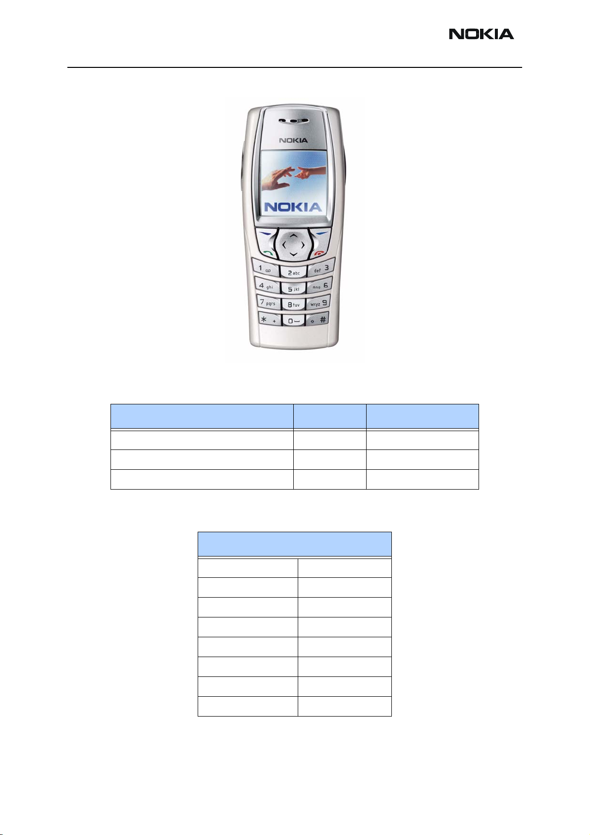
Nokia Model 6560 (RH-25)
RH-25 is a hand-portable dual band TDMA 850/1900 with AMPS. It has been designed
using DCT4 generation baseband (UEM/UPP), and RF (TACO) module, collectively referred
to as Stella processing engine.
The baseband module has been developed as part of the DCT4 common baseband.
RH-25 contains some baseband features that are new to the America's TDMA market.
These features include stereo FM receiver (offered as an accessory) and a MIDI (polyphonic ringing tones). RH-25 supports both two- and three-wire DCT3 chargers. The primary battery is the BLD-3 with a nominal capacity of 780 mAh.
Hardware Characteristics
• Hi-resolution (128x128) illuminated color display
• Active LCD pixel area: width 27.6mm X height 27.6mm
• Jack 4-style UI with four way navigation key; two soft key
• Support for internal semi-fixed battery (Janette type BLD-3)
• RTC backup battery support
• Audio amplifier and MALT speaker for MIDI support
• Ringing volume 100dB @ 5cm (MIDI tones through MALT speaker)
• Stereo FM receiver as an accessory
• IrDa port/interface
• Internal vibra
• Supports voice dial activation via headset button
• Six white TBSF LEDs for keyboard and two for LCD backlight
• 6-layer PWB, SMD with components on both sides of PWB
Issue 1 10/2003 Company Confidential ©2003 Nokia Corporation Page 3
Page 9
RH-25
General Information CCS Technical Documentation
Model 6560 Handset
Sales Package
Transceiver RH-25 Customer-specific
Battery (780 mAh Li-Ion) BLD-3 0670352
Rapid Performance Charger (US plug) ACP-12U 0675303
Module List
Name: Type Code Material Code
RH-25 (Nokia 6560)
A-cover assy 9491436
Keymat 9791041
Screws 6290171
Display 4850291
C-cover Module 9491370
Antenna Assy 0660298
Battery 0670352
B-cover 9653696
Page 4 ©2003 Nokia Corporation Company Confidential Issue 1 10/2003
Page 10
RH-25
CCS Technical Documentation General Information
Supported Accessories
Type Name Code
BLD-3 Standard 780 mAh Li-ion Battery 0670352
ACP-7U AC Travel Charger (US) 108-132 Vac 0675143
ACP-8U AC Charger 0675196
ACP-12U Rapid Performance Charger (US) 0675303
DDC-1 Spare Battery Charger 0675243
CA-8 Advanced Car Kit 0080932
BHF-1 Headrest handsfree 0273278
LPS-4 Loopset 0630443
LCH-12 Cigarette Lighter Charger 0675328
HDB-4 Boom Headset 0694094
HS-5 Earbud Headset 0694121
HDS-3 FM Stereo Headset 0694093
HS-3 Fashion Stereo Headset 0694156
HS-10 Retractable Headset 0694126
Technical Specifications
General Specifications of Transceiver RH-25
Parameter Specifications
Cellular system TDMA 800 and AMPS TDMA 1900
RX frequency band 869.01-893.97MHz 1930.05 - 1989.99MHz
TX frequency band 824.01-848.97MHz 1850.01 - 1909.95MHz
Number of RF channels 832 1999
Channel spacing 30KHz 30KHz
Power levels -5 - +28dBm /
0.3mW - 630mW
-5 - +28dBm /
0.3mW - 630mW
Parameter Mode Value and unit
Talk time Analog 2 hrs
Talk time Digital 5 hrs
Issue 1 10/2003 Company Confidential ©2003 Nokia Corporation Page 5
Page 11
RH-25
General Information CCS Technical Documentation
Parameter Mode Value and unit
Standby time Analog 60 hrs
Standby time Digital 371 hrs
Dimensions W=105.8mm L=44mm
Weight with BLD-3 battery 88.36g
Page 6 ©2003 Nokia Corporation Company Confidential Issue 1 10/2003
Page 12

CCS Technical Documentation
RH-25 Series Transceivers
Parts Lists
Issue 1 10/2003 Company Confidential ©2003 Nokia Corporation
Page 13

RH-25
Parts Lists CCS Technical Documentation
Contents
Page No
Exploded View............................................................................................................... 3
Assembly Parts of Basic Transceiver RH-25 ..............................................................4
Component Layout — Bottom ...................................................................................6
Parts Lists....................................................................................................................... 7
RH-25 (6560) — EDMS Issue 2.17 Code: 0202123 ...................................................7
Page 2 ©2003 Nokia Corporation Company Confidential Issue 1 10/2003
Page 14
RH-25
CCS Technical Documentation Parts Lists
Exploded View
Issue 1 10/2003 Company Confidential ©2003 Nokia Corporation Page 3
Page 15
RH-25
Parts Lists CCS Technical Documentation
Assembly Parts of Basic Transceiver RH-25
Item Qty Code Description
1 1 9491436 A-Cover (silver) DMC06279
2 1 9791041 Keymat (Latin) DMC06339
3 6 6290171 Screws M1.8x8mm DMC05300
4 1 9517301 Display Shield Assembly DMC06343
5 1 0210109 UI Board DMC06893
6 1 4850291 LCD Module DHS02568
7 1 9467111 LCD Frame DMC06344
8 1 9854768 PWB Engine DMF00140
9 1 5400243 DC Jack DNS04390
10 1 5409153 Battery Connector DNS01587
11 1 6800057
6800069
12 1 9453145 IR Window DMD10692
13 1 9790989 Power Key DMD10693
14 1 9491370 C-Cover DMC06323
15 1 9790990 Release Button DMD10665
16 1 9510845 Spring DNS05685
17 1 0660298 Antenna Assembly DMC06335
18 1 9491446 B-Cover Assembly (silver) DMC06280
Vibra Motor (Nomiki) DNS04642
Vibra Motor (Matsushita)
Page 4 ©2003 Nokia Corporation Company Confidential Issue 1 10/2003
Page 16
RH-25
CCS Technical Documentation Parts Lists
Component Layout — Top
Issue 1 10/2003 Company Confidential ©2003 Nokia Corporation Page 5
Page 17
RH-25
Parts Lists CCS Technical Documentation
Component Layout — Bottom
Page 6 ©2003 Nokia Corporation Company Confidential Issue 1 10/2003
Page 18
RH-25
CCS Technical Documentation Parts Lists
Parts Lists
RH-25 (6560) — EDMS Issue 2.17 Code: 0202123
Item Code Side X Y Description Value Type
R100 1430726 Bottom V 9 chip res 0W06 100R J 0402
R101 1430726 Bottom V 9 chip res 0W06 100R J 0402
R102 1430726 Bottom V 9 chip res 0W06 100R J 0402
R103 4120011 Bottom V 9 ZDIX4 IP4043CX5 CA 14V2 10W CSP5
R104 1430812 Bottom U 9 chip res 0W06 220K J 0402
R109 1430804 Top S 9 chip res 0W06 100K J 0402
R110 1825033 Bottom V 7 chip varistor VWM14V VC46V 0402
R111 1430804 Bottom T 9 chip res 0W06 100K J 0402
R112 1825033 Bottom V 7 chip varistor VWM14V VC46V 0402
R113 1825033 Bottom V 7 chip varistor VWM14V VC46V 0402
R114 1825033 Bottom V 7 chip varistor VWM14V VC46V 0402
R115 1825033 Bottom V 8 chip varistor VWM14V VC46V 0402
R116 1825033 Bottom V 8 chip varistor VWM14V VC46V 0402
R117 1430762 Bottom U 8 chip res 0W06 2K2 J 0402
R118 1430762 Bottom U 8 chip res 0W06 2K2 J 0402
R119 1430762 Bottom V 8 chip res 0W06 2K2 J 0402
R120 1430762 Bottom V 7 chip res 0W06 2K2 J 0402
R121 1430804 Top R 7 chip res 0W06 100K J 0402
R122 1430762 Bottom V 8 chip res 0W06 2K2 J 0402
R125 1430778 Bottom D 8 chip res 0W06 10K J 0402
R126 1825033 Top D 6 chip varistor VWM14V VC46V 0402
R150 1620031 Bottom U 8 res network 0W06 2X1K0 J 0404
R152 1430784 Top S 8 chip res 0W06 15K J 0402
R153 1430778 Top S 10 chip res 0W06 10K J 0402
R161 1825033 Top F 7 chip varistor VWM14V VC46V 0402
R162 1825033 Top E 7 chip varistor VWM14V VC46V 0402
R163 1430764 Bottom T 6 chip res 0W06 3K3 J 0402
R164 1430710 Bottom U 7 chip res 0W06 22R J 0402
R165 1430710 Bottom U 6 chip res 0W06 22R J 0402
Issue 1 10/2003 Company Confidential ©2003 Nokia Corporation Page 7
Page 19
RH-25
Parts Lists CCS Technical Documentation
Item Code Side X Y Description Value Type
R166 1430710 Bottom U 7 chip res 0W06 22R J 0402
R167 1430710 Bottom U 6 chip res 0W06 22R J 0402
R200 1414605 Bottom T 9 chip res 0W25 0R22 J 0805
R202 1430804 Top S 7 chip res 0W06 100K J 0402
R203 1430087 Top S 7 chip res 0W06 100K J 0603
R204 1430087 Top S 7 chip res 0W06 100K J 0603
R205 1430770 Top S 7 chip res 0W06 4K7 J 0402
R206 1430804 Top R 7 chip res 0W06 100K J 0402
R225 1430770 Top S 7 chip res 0W06 4K7 J 0402
R226 1430690 Top R 7 chip res jumper 0R0 0402
R227 1430690 Top R 7 chip res jumper 0R0 0402
R300 1430712 Top T 10 chip res 0W06 27R J 0402
R301 1430734 Bottom O 4 chip res 0W06 220R J 0402
R302 1430734 Bottom O 4 chip res 0W06 220R J 0402
R303 1430734 Bottom O 4 chip res 0W06 220R J 0402
R307 1825033 Bottom O 6 chip varistor VWM14V VC46V 0402
R308 1430740 Top O 6 chip res 0W06 2K2 J 0402
R309 1430740 Top O 7 chip res 0W06 2K2 J 0402
R350 1413850 Bottom D 9 chip res 0W125 4R7 J 0805
R420 1430268 Top O 8 chip res 0W06 27K F
100PPM
R450 1430770 Top O 6 chip res 0W06 4K7 J 0402
R709 1430700 Top L 9 chip res 0W06 10R J 0402
R712 1430700 Top K 10 chip res 0W06 10R J 0402
R721 1430796 Top J 9 chip res 0W06 47K J 0402
R741 1430796 Top K 10 chip res 0W06 47K J 0402
0603
R771 1430786 Top N 6 chip res 0W06 18K J 0402
R772 1430726 Top N 7 chip res 0W06 100R J 0402
R773 1430700 Top N 7 chip res 0W06 10R J 0402
R774 1430700 Top L 7 chip res 0W06 10R J 0402
R791 1430778 Top N 9 chip res 0W06 10K J 0402
R792 1430700 Top M 9 chip res 0W06 10R J 0402
Page 8 ©2003 Nokia Corporation Company Confidential Issue 1 10/2003
Page 20
RH-25
CCS Technical Documentation Parts Lists
Item Code Side X Y Description Value Type
R818 1430268 Top I 7 chip res 0W06 27K F
100PPM
R820 1430740 Top I 7 chip res 0W06 2K2 J 0402
R830 1430832 Top N 8 chip res 0W06 2K7 J 0402
R831 1430734 Top K 8 chip res 0W06 220R J 0402
R850 1430798 Top D 10 chip res 0W06 56K J 0402
R851 1430734 Top E 10 chip res 0W06 220R J 0402
C100 2315201 Bottom V 7 chip array NP0 2X27P K 25V 0405
C101 2320481 Bottom T 9 chip cap X5R 1U K 6V3 0603
C102 2320481 Bottom V 9 chip cap X5R 1U K 6V3 0603
C103 2320544 Top S 9 chip cap NP0 22P J 50V 0402
C105 2312201 Bottom U 6 chip cap X5R 4U7 K 6V3 T=0.95 0805
C106 2312201 Bottom U 7 chip cap X5R 4U7 K 6V3 T=0.95 0805
C107 2320544 Top O 10 chip cap NP0 22P J 50V 0402
C108 2320544 Top O 10 chip cap NP0 22P J 50V 0402
0603
C109 2320783 Top S 8 chipcap X7R 100N K 16V 0603
C110 2320546 Bottom U 8 chip cap NP0 27P J 50V 0402
C111 2320544 Bottom U 8 chip cap NP0 22P J 50V 0402
C112 2320778 Bottom V 9 chip cap X7R 10N K 16V 0402
C113 2320544 Bottom U 8 chip cap NP0 22P J 50V 0402
C114 2320544 Bottom V 8 chip cap NP0 22P J 50V 0402
C115 2320756 Bottom V 8 chip cap X7R 3N3 K 50V 0402
C116 2320756 Bottom V 8 chip cap X7R 3N3 K 50V 0402
C117 2320544 Bottom V 8 chip cap NP0 22P J 50V 0402
C118 2320544 Bottom V 8 chip cap NP0 22P J 50V 0402
C119 2320744 Top S 7 chip cap X7R 1N0 K 50V 0402
C120 2320536 Top U 9 chip cap NP0 10P J 50V 0402
C121 2315201 Bottom V 9 chip array NP0 2X27P K 25V 0405
C122 2320805 Top F 4 chip cap X5R 100N K 10V 0402
C123 2320544 Top S 8 chip cap NP0 22P J 50V 0402
C124 2320744 Bottom T 10 chip cap X7R 1N0 K 50V 0402
C125 2320544 Top D 6 chip cap NP0 22P J 50V 0402
C126 2320536 Top U 9 chip cap NP0 10P J 50V 0402
Issue 1 10/2003 Company Confidential ©2003 Nokia Corporation Page 9
Page 21
RH-25
Parts Lists CCS Technical Documentation
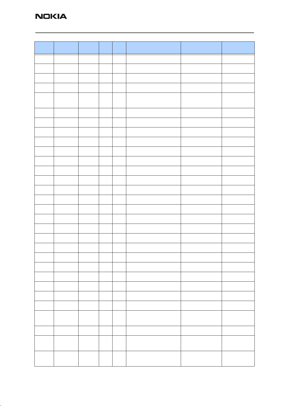
Item Code Side X Y Description Value Type
C127 2320546 Bottom Q 10 chip cap NP0 27P J 50V 0402
C128 2320596 Top F 7 chip cap X7R 3N3 J 50V 0402
C130 2320552 Bottom R 5 chip cap NP0 47P J 50V 0402
C131 2320552 Bottom O 7 chip cap NP0 47P J 50V 0402
C132 2320552 Bottom R 5 chip cap NP0 47P J 50V 0402
C133 2320544 Top T 5 chip cap NP0 22P J 50V 0402
C134 2320544 Top T 5 chip cap NP0 22P J 50V 0402
C135 2320544 Top T 5 chip cap NP0 22P J 50V 0402
C137 2320552 Top T 6 chip cap NP0 47P J 50V 0402
C138 2320552 Top T 6 chip cap NP0 47P J 50V 0402
C139 2320552 Top T 7 chip cap NP0 47P J 50V 0402
C151 2320783 Top S 9 chip cap X7R 100N K 16V 0603
C155 2320783 Top S 9 chip cap X7R 100N K 16V 0603
C156 2320783 Top S 9 chip cap X7R 100N K 16V 0603
C157 2320560 Top R 9 chip cap NP0 100P J 50V 0402
C158 2315201 Bottom V 7 chip array NP0 2X27P K 25V 0405
C159 2320560 Top R 8 chip cap NP0 100P J 50V 0402
C160 2320805 Bottom T 6 chip cap X5R 100N K 10V 0402
C161 2320805 Bottom T 6 chip cap X5R 100N K 10V 0402
C163 2320805 Top S 8 chip cap X5R 100N K 10V 0402
C164 2320596 Top F 7 chip cap X7R 3N3 J 50V 0402
C166 2320481 Bottom T 6 chip cap X5R 1U K 6V3 0603
C167 2320481 Bottom T 6 chip cap X5R 1U K 6V3 0603
C169 2320805 Bottom T 7 chip cap X5R 100N K 10V 0402
C200 2320552 Bottom N 7 chip cap NP0 47P J 50V 0402
C201 2320481 Top P 10 chip cap X5R 1U K 6V3 0603
C202 2320548 Bottom T 9 chip cap NP0 33P J 50V 0402
C203 2320536 Top S 10 chip cap NP0 10P J 50V 0402
C204 2320536 Top S 9 chip cap NP0 10P J 50V 0402
C205 2320481 Top Q 10 chip cap X5R 1U K 6V3 0603
C206 2320481 Top R 10 chip cap X5R 1U K 6V3 0603
C207 2320481 Top S 8 chip cap X5R 1U K 6V3 0603
Page 10 ©2003 Nokia Corporation Company Confidential Issue 1 10/2003
Page 22

RH-25
CCS Technical Documentation Parts Lists
Item Code Side X Y Description Value Type
C208 2320481 Top O 10 chip cap X5R 1U K 6V3 0603
C211 2320481 Top R 10 chip cap X5R 1U K 6V3 0603
C212 2320481 Top R 10 chip cap X5R 1U K 6V3 0603
C213 2320481 Top Q 10 chip cap X5R 1U K 6V3 0603
C215 2320481 Top S 8 chip cap X5R 1U K 6V3 0603
C217 2320778 Top S 7 chip cap X7R 10N K 16V 0402
C218 2320805 Top P 6 chip cap X5R 100N K 10V 0402
C219 2320125 Top P 10 chip cap X5R 1U K 16 V 0603
C220 2320778 Top R 7 chip cap X7R 10N K 16V 0402
C221 2320481 Top O 10 chip cap X5R 1U K 6V3 0603
C222 2320481 Top O 10 chip cap X5R 1U K 6V3 0603
C223 2320481 Top P 9 chip cap X5R 1U K 6V3 0603
C224 2320481 Top O 9 chip cap X5R 1U K 6V3 0603
C226 2320481 Top O 8 chip cap X5R 1U K 6V3 0603
C228 2320481 Top O 8 chip cap X5R 1U K 6V3 0603
C229 2320481 Top O 8 chip cap X5R 1U K 6V3 0603
C230 2320778 Top R 7 chip cap X7R 10N K 16V 0402
C231 2320481 Top P 8 chip cap X5R 1U K 6V3 0603
C232 2320481 Top P 9 chip cap X5R 1U K 6V3 0603
C234 2320481 Top P 9 chip cap X5R 1U K 6V3 0603
C235 2320805 Top S 8 chip cap X5R 100N K 10V 0402
C236 2320805 Top P 8 chip cap X5R 100N K 10V 0402
C237 2320805 Top P 8 chip cap X5R 100N K 10V 0402
C238 2320491 Top P 10 chip cap X7R 220N K 10V 0603
C239 2320805 Top R 7 chip cap X5R 100N K 10V 0402
C241 2320544 Top S 8 chip cap NP0 22P J 50V 0402
C242 2320544 Top S 8 chip cap NP0 22P J 50V 0402
C245 2320481 Top O 9 chip cap X5R 1U K 6V3 0603
C261 2312243 Top O 9 chip cap X5R 4U7 K 6V3 0805
C262 2312243 Top Q 10 chip cap X5R 4U7 K 6V3 0805
C264 2320481 Top S 7 chip cap X5R 1U K 6V3 0603
C302 2320556 Top T 9 chip cap NP0 68P J 50V 0402
Issue 1 10/2003 Company Confidential ©2003 Nokia Corporation Page 11
Page 23

RH-25
Parts Lists CCS Technical Documentation
Item Code Side X Y Description Value Type
C303 2320125 Top T 9 chip cap X5R 1U K 16 V 0603
C304 2320125 Bottom O 6 chip cap X5R 1U K 16 V 0603
C307 2320548 Top U 4 chip cap NP0 33P J 50V 0402
C308 2320560 Top U 4 chip cap NP0 100P J 50V 0402
C350 2320805 Bottom D 9 chip cap X5R 100N K 10V 0402
C351 2312243 Top D 8 chip cap X5R 4U7 K 6V3 0805
C361 2320805 Bottom D 9 chip cap X5R 100N K 10V 0402
C400 2320778 Top P 6 chip cap X7R 10N K 16V 0402
C401 2320805 Top P 7 chip cap X5R 100N K 10V 0402
C402 2320778 Top Q 7 chip cap X7R 10N K 16V 0402
C403 2320778 Top Q 7 chip cap X7R 10N K 16V 0402
C404 2320778 Top Q 7 chip cap X7R 10N K 16V 0402
C405 2320778 Top P 6 chip cap X7R 10N K 16V 0402
C420 2320744 Top P 6 chip cap X7R 1N0 K 50V 0402
C450 2320778 Top P 6 chip cap X7R 10N K 16V 0402
C451 2320805 Top O 6 chip cap X5R 100N K 10V 0402
C454 2320779 Top O 6 chip cap X74 100N K 16V 0603
C700 2320552 Top I 8 chip cap NP0 47P J 50V 0402
C701 2320536 Top I 8 chip cap NP0 10P J 50V 0402
C702 2320805 Top I 8 chip cap X5R 100N K 10V 0402
C703 2320536 Top I 8 chip cap NP0 10P J 50V 0402
C704 2320805 Top I 8 chip cap X5R 100N K 10V 0402
C706 2320552 Top K 9 chip cap NP0 47P J 50V 0402
C707 2320744 Top K 9 chip cap X7R 1N0 K 50V 0402
C708 2320481 Top L 9 chip cap X5R 1U K 6V3 0603
C710 2320740 Top J 9 chip cap X7R 680P K 50V 0402
C711 2320481 Top J 10 chip cap X5R 1U K 6V3 0603
C712 2320552 Top K 9 chip cap NP0 47P J 50V 0402
C720 2320564 Top J 9 chip cap NP0 150P J 50V 0402
C721 2322023 Top J 9 chip cap NP0 2N2 J 16V 0603
C740 2320564 Top K 9 chip cap NP0 150P J 50V 0402
C741 2322023 Top L 10 chip cap NP0 2N2 J 16V 0603
Page 12 ©2003 Nokia Corporation Company Confidential Issue 1 10/2003
Page 24

RH-25
CCS Technical Documentation Parts Lists
Item Code Side X Y Description Value Type
C770 2320580 Top M 6 chip cap X7R 680P J 50V 0402
C771 2480003 Top M 6 chip cap PPS 8N2 J 16V 0805
C772 2320495 Top M 6 chip cap NP0 1N0 J 50V 0603
C773 2320466 Top M 7 chip cap NP0 220P J 50V 0603
C774 2320536 Top K 7 chip cap NP0 10P J 50V 0402
C775 2320481 Top K 7 chip cap X5R 1U K 6V3 0603
C776 2320778 Top L 7 chip cap X7R 10N K 16V 0402
C777 2320536 Top K 6 chip cap NP0 10P J 50V 0402
C778 2320536 Top K 6 chip cap NP0 10P J 50V 0402
C791 2320805 Top N 10 chip cap X5R 100N K 10V 0402
C792 2320778 Top N 9 chip cap X7R 10N K 16V 0402
C793 2320481 Top N 9 chip cap X5R 1U K 6V3 0603
C801 2320552 Top J 7 chip cap NP0 47P J 50V 0402
C802 2320778 Top J 7 chip cap X7R 10N K 16V 0402
C803 2320536 Top J 7 chip cap NP0 10P J 50V 0402
C806 2320552 Top K 8 chip cap NP0 47P J 50V 0402
C807 2320536 Top K 8 chip cap NP0 10P J 50V 0402
C808 2320805 Top L 9 chip cap X5R 100N K 10V 0402
C820 2320552 Top J 7 chip cap NP0 47P J 50V 0402
C821 2320552 Top K 7 chip cap NP0 47P J 50V 0402
C822 2320805 Top K 7 chip cap X5R 100N K 10V 0402
C830 2320778 Top N 8 chip cap X7R 10N K 16V 0402
C831 2320602 Top M 8 chip cap NP0 4P7 C 50V 0402
C832 2320602 Top M 8 chip cap NP0 4P7 C 50V 0402
C833 2320536 Top K 8 chip cap NP0 10P J 50V 0402
C834 2320536 Top K 8 chip cap NP0 10P J 50V 0402
C850 2320536 Top D 9 chip cap NP0 10P J 50V 0402
C851 2320536 Top D 10 chip cap NP0 10P J 50V 0402
C852 2320584 Top D 10 chip cap X7R 1N0 J50V 0402
C853 2320554 Top E 9 chip cap NP0 56P J 50V 0402
C854 2320554 Top E 10 chip cap NP0 56P J 50V 0402
C857 2320536 Top E 10 chip cap NP0 10P J 50V 0402
Issue 1 10/2003 Company Confidential ©2003 Nokia Corporation Page 13
Page 25

RH-25
Parts Lists CCS Technical Documentation
Item Code Side X Y Description Value Type
C858 2320584 Top F 10 chip cap X7R 1N0 J50V 0402
C859 2320536 Top K 7 chip cap NP0 10P J 50V 0402
C861 2320514 Top F 10 chip cap NP0 1P2 C 50V 0402
C910 2320744 Top I 4 chip cap X7R 1N0 K 50V 0402
C911 2320778 Top J 5 chip cap X7R 10N K 16V 0402
C913 2320560 Top J 5 chip cap NP0 100P J 50V 0402
C914 2320481 Top J 5 chip cap X5R 1U K 6V3 0603
C915 2320536 Top I 9 chip cap NP0 10P J 50V 0402
C916 2320805 Top I 9 chip cap X5R 100N K 10V 0402
C919 2320508 Top H 5 chip cap NP0 1P0 C 50V 0402
C923 2320604 Top I 9 chip cap NP0 18P J 50V 0402
C924 2320604 Top K 4 chip cap NP0 18P J 50V 0402
C930 2320536 Top H 7 chip cap NP0 10P J 50V 0402
C931 2320744 Top G 6 chip cap X7R 1N0 K 50V 0402
C960 2320536 Top J 10 chip cap NP0 10P J 50V 0402
C961 2320536 Top J 10 chip cap NP0 10P J 50V 0402
C962 2320536 Top H 9 chip cap NP0 10P J 50V 0402
C963 2320536 Top H 9 chip cap NP0 10P J 50V 0402
C965 2320508 Top G 9 chip cap NP0 1P0 C 50V 0402
C967 2320536 Top G 7 chip cap NP0 10P J 50V 0402
C968 2320778 Top H 9 chip cap X7R 10N K 16V 0402
C970 2320536 Top J 5 chip cap NP0 10P J 50V 0402
C971 2320536 Top J 9 chip cap NP0 10P J 50V 0402
C972 2320805 Top J 9 chip cap X5R 100N K 10V 0402
C975 2320560 Top J 10 chip cap NP0 100P J 50V 0402
L100 3203743 Bottom U 10 ferrite bead 0R03 42R/100MHz 3A 0805
L103 3203803 Bottom V 7 chip bead array 2X1000R 0R75 0405
L104 3203803 Bottom V 7 chip bead array 2X1000R 0R75 0405
L106 3203741 Bottom V 9 ferrite bead 0R5 600R/100MHz 0603
L107 3203741 Bottom V 9 ferrite bead 0R5 600R/100MHz 0603
L131 3203803 Top O 10 chip bead array 2X1000R 0R75 0405
L151 3645349 Top F 7 chip coil 33NH G Q40/250MHz 0603
Page 14 ©2003 Nokia Corporation Company Confidential Issue 1 10/2003
Page 26
RH-25
CCS Technical Documentation Parts Lists
Item Code Side X Y Description Value Type
L152 3645349 Top E 7 chip coil 33NH G Q40/250MHz 0603
L160 3203741 Bottom V 8 ferrite bead 0R5 600R/100MHz 0603
L161 3203741 Bottom V 8 ferrite bead 0R5 600R/100MHz 0603
L164 3203741 Bottom V 7 ferrite bead 0R5 600R/100MHz 0603
L300 3640119 Top U 10 Choke 22U M 1R4
0.33A
L730 3645093 Top K 9 chip coil 36N G Q55/500MHz 0805
L746 3645091 Top K 9 chip coil 22N G Q55/500MHz 0805
L820 3645211 Top K 7 chip coil 6N8 K Q27/250MHz 0603
L821 3646069 Top J 7 chip coil 33N J Q23/800MHz 0402
L822 3646063 Top J 7 chip coil 22N J Q28/800MHz 0402
L830 3643087 Top M 8 chip coil 180N J Q13/50MHz 0805
L831 3643087 Top M 8 chip coil 180N J Q13/50MHz 0805
L832 3645067 Top L 8 chip coil 330N J Q48/250MHz 0805
L851 3646005 Top D 9 chip coil 2N7+- 0N3 Q29/800MHz 0402
L852 3646067 Top E 10 chip coil 18N J Q29/800MHz 0402
L855 3646053 Top E 9 chip coil 4N7+-0N3 Q28/800MHz 0402
L903 3643085 Top J 5 chip coil 5N6+/-0N5 Q35 1.5A 0805
L960 3646083 Top J 10 chip coil 100N J Q16/300MHz 0402
3.3X3.3X1.5
L961 3646083 Top J 10 chip coil 100N J Q16/300MHz 0402
L962 3646083 Top I 10 chip coil 100N J Q16/300MHz 0402
L963 3646083 Top I 10 chip coil 100N J Q16/300MHz 0402
V100 4113721 Bottom U 9 TVS DI 1PMT16AT3 16V 175W PWRMITE
V300 4110475 Top T 10 SCH DI 1PS79SB31 200MA 30V SOD523
V850 4210189 Top E 10 TR BFP620
D200 4370825 Top Q 8 UEMK W-DOG ENA TO21 TFBGA168
D400 4370873 Top R 5 UPP8M V2.2 F751986B C035 UBGA144
D450 4341531 Top P 5 Combo 64M NOR+4M
SRAM
G780 4350279 Top L 6 VCO 2GHz 2.78V 10.5MA TDMA
G790 4510307 Top M 9 VCTCXO 19.44MHz+/-
2.5PPM
N100 4341063 Bottom U 9 REG 2.8V/150MA
(LP3985NOPB)
TBGA48
2.78V
SOT23-5
Issue 1 10/2003 Company Confidential ©2003 Nokia Corporation Page 15
Page 27
RH-25
Parts Lists CCS Technical Documentation
Item Code Side X Y Description Value Type
N150 4341417 Bottom T 6 AF Amp 85MW/5V
(LM4855ITLX)
N300 4341309 Top T 10 DC/DC CONV 350MA
(TK11851)
N801 4370915 Top J 8 TACO_V3.1 TZC8CRTT TFBGA108
N901 4350401 Top I 5 PW AMP RF9270 TDMA800
N930 4350267 Top H 6 Pwr Detector Module 800/1900MHz
N960 4350399 Top H 8 Pw Amp RF9271 TDMA1900
N961 4860171 Top D 9 IRDA 1.3 1.152MBIT/S
>2.4V 8PIN
Z100 3640085 Top U 9 FILT 470NF 16V OR03 2A 0805
Z301 4120031 Bottom O 5 EMI/ESD FILT EMIF10-1K010F1 BGA24
Z820 4510357 Top J 6 Saw Filt 881.5+-12.5MHz/
3DB
Z830 4511351 Top L 8 Saw Filt 135.54+-
0.013MHz
Z850 4511361 Top I 6 Saw Filt 1960+-30MHz/
4.5DB
USME18
SOP8
2.5X2
6X3.5MM
2X2.5
Z905 4511357 Top J 4 Saw Filt 836.5+-12.5MHz/
3.0
Z906 4512173 Top G 5 Dupl 824-849/869-
894MHz
Z907 4550117 Top E 5 Dupl 824-894/1850-
1990MHz
Z960 4511353 Top I 10 Saw Filt 180.51+-
0.015MHz
Z961 4511363 Top G 9 Saw Filt 1880+-30MHz/
5DB
Z962 4512171 Top E 7 Dupl 1850-1910/1930-
1990MHz
T775 4550153 Top K 6 Transf Balun 2060+-70MHz 2.0X1.25
T960 4550173 Top H 9 Trans Balun 1920+-70MHz 2X1.25
T961 3640429 Top I 9 Transf Balun 900 MHz +/- 100
MHz
B200 4510303 Top S 9 Crystal 32.768KHz+-
20PPM 12.
2.5X2
5X5X1.7
3.2X1.6
3X3MM
2.5X2X1
17X5
1206
5PF
F100 5119019 Bottom V 9 Sm Fuse F 1.5A 32V 0603
X101 5460061 Top W 6 Sm System Connector 14POL
Page 16 ©2003 Nokia Corporation Company Confidential Issue 1 10/2003
Page 28
RH-25
CCS Technical Documentation Parts Lists
Item Code Side X Y Description Value Type
X301 5469135 Bottom N 5 Sm Conn 2X8 SPR 50V 0.5A PWB/PWB
X302 5469175 Bottom D 5 Sm Conn 2X5F P0.5 PWB/PWB
X900 5429037 Top E 5 Sm Conn Fr Jack 50R 2W 6GHz
A100 9517299 Top Q 7 BB Shield Assy DMC06338 Hobbes
A900 9517302 Top J 7 RF Shield Assy DMC06337 Hobbes
S001 5409235 Top C 5 Sm Tact Sw Trav 0.2 4.1X3.55X
1.75
Issue 1 10/2003 Company Confidential ©2003 Nokia Corporation Page 17
Page 29

RH-25
Parts Lists CCS Technical Documentation
Page 18 ©2003 Nokia Corporation Company Confidential Issue 1 10/2003
Page 30

CCS Technical Documentation
RH-25 Series Transceivers
Service Software Instructions
Issue 1 10/2003 Company Confidential ©2003 Nokia Corporation
Page 31

RH-25
Service Software Instructions CCS Technical Documentation
Contents
Page No
Phoenix User’s Guide .................................................................................................... 3
Introduction ..................................................................................................................3
General Setup Procedure........................................................................................... 3
Hardware Requirements for using Phoenix .............................................................. 4
Installing Phoenix ........................................................................................................4
Installation Directions............................................................................................... 4
Software Support Bundles ...........................................................................................4
Starting a Phoenix Session ...........................................................................................5
Concepts.................................................................................................................... 5
Initial Session with Phoenix...................................................................................... 5
Scanning for a Product.............................................................................................. 6
Using Components.................................................................................................... 7
Using Profiles............................................................................................................ 7
Uninstalling Phoenix ...................................................................................................7
Uninstalling Phoenix version.................................................................................... 7
Page 2 ©2003 Nokia Corporation Company Confidential Issue 1 10/2003
Page 32

RH-25
CCS Technical Documentation Service Software Instructions
Phoenix User’s Guide
Introduction
This section briefly describes how to install Phoenix and includes some basic information
on how to use the program. More detailed information can be found in the Phoenix Help
files. Each feature in Phoenix has its own Help file, which can be activated whil running
Phoenix. To activate a Help file while Phoenix is running, press the F1 key or the specific
feature’s Help button.
General Setup Procedure
Initial installation of Phoenix requires the complete Phoenix installation package. This
package, currently around 30 Megabytes in size, is provided on a CD-ROM disk. Because
of this large size, it is not recommended to download the file nor is it practical to provide
it on 3.5-inch floppy disks.
Install Phoenix by following the steps outlined on the material that comes with the disk.
It should be noted that installation of a Nokia dongle on the computer being loaded is
REQUIRED prior to beginning the installation of the software.
The software is packaged into an Installshield executable bundle. When the user doubleclicks on this file, the installation program provides on-screen instructions on how to
proceed. Standard installation, provided by selecting all default choices, is highly recommended. You may do a custom installation and place Phoenix into a special location on
your hard drive, but this is only recommended for experienced users.
It is necessary to reboot the computer after installing the software. The program will not
be usable until a reboot is performed. After reboot, the Phoenix icon is displayed on the
computer desktop. Double-clicking on this icon launches the program.
Issue 1 10/2003 Company Confidential ©2003 Nokia Corporation Page 3
Page 33

RH-25
Service Software Instructions CCS Technical Documentation
Hardware Requirements for using Phoenix
Minimum Hardware Requirements
Processor 233 MHz
RAM1 64 MB
Disk space needed 50-100 MB
Supported Operating
Windows 95 Limited, no USB support
Windows 98
Windows NT 4.0 no USB support
Windows 2000 Professional version
Installing Phoenix
Before installing the software, verify:
• The dongle is attached to the parallel port for PKD version dongles, or an FLS-4 version
dongle is attached on either the parallel port or the USB port (if the computer supports
USB).
• Ensure that if the computer supports administrator rights (typically on Windows NT
and Windows 2000 installations) that access is enabled for the user performing the
Phoenix installation.
• If a previous version of Phoenix has been installed, it may be necessary to first properly
remove that program prior to installing the new version. If installation is performed,
be sure to reboot the computer prior to continuing. See the section Uninstalling
Phoenix for instructions on how to uninstall.
Systems
Notes
Installation Directions
• Insert the CD-ROM disk into the computer drive
• Access the drive and double-click on the Phoenix software package found on the CD.
• Follow the on-screen prompts to conclusion.
Note that rebooting the computer may be necessary when completed.
Software Support Bundles
The Phoenix installation is auto-executable. You must obtain Software Support Bundles
Page 4 ©2003 Nokia Corporation Company Confidential Issue 1 10/2003
Page 34

RH-25
CCS Technical Documentation Service Software Instructions
to load software upgrade files to customer-specific phone models.
These bundles are created by CCS and made available by AMS on the Partners Web Page
http://americas.partners.nokia.com. This web page is password-controlled; if you have
not registered as a user, contact Nokia Central Service in Melbourne, Florida.
Similar to the Phoenix installation, these Software Support Bundles are InstallShield executable packages. Just double-click on the package and it will auto-install.
No rebooting of the computer is required.
Starting a Phoenix Session
Concepts
When referring to Phoenix, Product is the cellular phone attached to the computer.
More specifically, it is the particular type of phone.
Connection is the type of cable used to attach the phone and the port on the computer
where it is attached. Refer to the Service Tools chapter for additional information.
The first time Phoenix is used, certain connection configurations must be made. Subsequent uses will rely on these selections and they will not need to be made again.
Initial Session with Phoenix
It is necessary to create the connection the first time Phoenix is used. Follow these simple steps:
Select Manage Connections… from the “File” drop-down menu.
Issue 1 10/2003 Company Confidential ©2003 Nokia Corporation Page 5
Page 35

RH-25
Service Software Instructions CCS Technical Documentation
Next click the Add… button to create a new connection.
When the Select Mode dialog box appears, you may then select either Wizard, which will
auto-detect your connection configuration, or Manual, which allows you to manually
select options to create the connection.
Once a connection is defined, make sure that the one to be used is moved to the top of
the list (use the up down arrows on the Manage Connections dialog box. Then click on
the Apply button. Close the window when finished.
You can now proceed with the normal initiation of a session by selecting a product or
scanning for a product.
Scanning for a Product
Many features of this program are product-specific. Therefore it is necessary to configure Phoenix for the product on which you will be working at the beginning of the session.
Scan Product – Choose Scan Product from the drop-down menu list and Phoenix will
automatically scan for product and select the necessary configurations. The status bar
Page 6 ©2003 Nokia Corporation Company Confidential Issue 1 10/2003
Page 36

RH-25
CCS Technical Documentation Service Software Instructions
at the bottom will indicate if the product was found and its type.
Using Components
When working with Phoenix, tasks are generally managed by specific software components. From the menu, select the desired component or task to be performed.
“Opening a component” is defined as opening a tool window within Phoenix. When this
window is opened, Phoenix also opens a toolbar for it and adds component-specific
menu items in the Window menu.
Using Profiles
Phoenix’s Profile feature allows product, connection and currently open components to
be stored into permanent storage by creating a profile file with a name of your choice
followed by an .nmp file extension for later retrieval.
Saved profiles makes it easy to configure Phoenix into a desired configuration with
favorite windows already opened and ready to go.
Opening and saving profiles is done via menu commands found in the File drop-down
menu: Open Profile and Save Profile.
Profiles are stored into a disk file with user-defined names. As a result, there can be
multiple profiles for different repeated tasks or user preferences.
Uninstalling Phoenix
As mentioned in the Installing Phoenix section, it may be necessary or desirable to
remove Phoenix. Care must be taken to follow this procedure. Failure to remove the
program properly will cause misconfiguration of the computer’s registry.
Uninstalling Phoenix version
• Access the computer’s “Control Panel” section, selectable from the Start button or the
“My Computer” desktop icon
• Select the “Add/Remove Programs” icon
• Select the Phoenix version to be removed, and click the Add/Remove button
• Click on the OK button to begin the process of removal
• Follow the on-screen instructions
Be sure to reboot the computer when finished.
Issue 1 10/2003 Company Confidential ©2003 Nokia Corporation Page 7
Page 37

RH-25
Service Software Instructions CCS Technical Documentation
Page 8 ©2003 Nokia Corporation Company Confidential Issue 1 10/2003
Page 38

CCS Technical Documentation
RH-25 Series Transceivers
Service Tools
Issue 1 10/2003 Confidential © 2003 Nokia Corporation
Page 39

RH-25
Service Tools CCS Technical Documentation
Contents
Page No
Service Tools.................................................................................................................. 3
6560 .............................................................................................................................3
Flashing and Testing Setups .......................................................................................... 8
FPS-8 Flash Prommer for Heavy Flash .......................................................................8
FPS-8C Flash Prommer for Heavy Parallel Flash .......................................................8
User Instructions ............................................................................................................ 9
DA-15 / SA-16 .............................................................................................................9
SF-15 ..........................................................................................................................11
Page 2 ©2003 Nokia Corporation Confidential Issue 1 10/2003
Page 40

RH-25
CCS Technical Documentation Service Tools
Service Tools
6560
Photo Code Service Tool Code Description
MJ-16 Module Jig 0770575 This jig allows phone
PWB-level service and
troubleshooting. Electric currents should be
protected against
over-voltage and
over-current.
FLS-4S POS Flash Adapter 0080543 The Point of Sale
(POS) flash is a lowcost software upgrade
tool. This requires the
XCS-1 cable and
ACP-8U for operation.
FPS-8 Flash Prommer 0080321 The Flash Prommer
FPS-8 is used for
flash.
FPS-8C Heavy Flash Prommer 0080396 The Heavy Flash
Prommer FPS-8C is
used for heavy parallel flashing.
Issue 1 10/2003 Confidential ©2003 Nokia Corporation Page 3
Page 41

RH-25
Service Tools CCS Technical Documentation
Photo Code Service Tool Code Description
JBV-1 Docking Station 0770298 The Docking Station
and the Docking Station Adapter (DA-15)
are needed for Mbus,
Fbus, RF, and audio
connections.
This setup allows connection between flash
prommers. When the
audio box is connected, it has to be
connected to the
phone’s audio connector.
DA-15 Docking Station
Adapter
CPL-1 Coupler 0770287 The coupler has been
JBA-8 Audio Box 0770320 The Audio Box is
0770624 The Docking Station
can be powered by
FPS-8 or external
power supply.
NOTE: SEE USER
INSTRUCTIONS FOR
DA-15 on page 9.
developed for antenna
go/no go testing.
needed for audio connections. The box
must support DCT4
Janette audios. JBA-8
provides an interconnection between the
phone’s system connector (XEAR, XMIC)
through a fixed audio
cable and audio tester
with a BNC-BNC
coax. Connection to a
PC can be made with
the service battery,
through a DAU-9
cable.
Page 4 ©2003 Nokia Corporation Confidential Issue 1 10/2003
Page 42

RH-25
CCS Technical Documentation Service Tools
Photo Code Service Tool Code Description
SF-15 Flash Adapter 0770625 SF-15 allows a con-
tinuous maximum
power supply for the
phone from an external power supply, the
ACP-8.
NOTE: SEE USER
INSTRUCTIONS FOR
SF-15 ON PAGE 11.
Note: SF-15 is not to
be used for handset
testing; it is only
designed for flashing.
AXP-8 Printer Cable 073F000 The Parallel Printer
Cable connects the
parallel connector of
the PC and the parallel input of the FPS-8.
AXS-4 D9-D9 Cable 0730090 The AXS-4 D9-D9
service cable is used
to connect two 9-pin
connectors (e.g.,
between PC and
FPS-8). AXS-4 length
is 2 meters
CA-X Audio Cable TBD The audio cable con-
nects to the audio box
JBA-8.
SCB-3 DC Cable 0730114 The DC Cable SCB-3 is
used to connect the
docking station to the
charger connection
(Vin) of the phone to
conduct the charger
calibration service
procedure.
Issue 1 10/2003 Confidential ©2003 Nokia Corporation Page 5
Page 43

RH-25
Service Tools CCS Technical Documentation
Photo Code Service Tool Code Description
DAU-9S Mbus Cable 0730108 The Mbus Cable has a
modular connector
and is used with the
service audio box
JBA-4 or a modular
T-adapter.
PCS-1 Power Cable 0730012 The Power Cable
PCS-1 is used to connect the service tools
(JBV-1, MJF-23) to
an external power
supply.
XRF-1 RF Cable 0730085 The XRF-1 cable con-
nects a service tool
and RF measurement
equipment.
XCS-4 Mbus/Fbus Cable 0730178 The XCS-4 Service
Cable is a modular
cable for flashing
DCT4 products.
Page 6 ©2003 Nokia Corporation Confidential Issue 1 10/2003
Page 44

RH-25
CCS Technical Documentation Service Tools
Photo Code Service Tool Code Description
PKD-1 SW Security Device 0750018 SW security device
PKD-1 is hardware
device that, when
connected to the parallel (LPT) port of the
PC, enables the use of
the service software.
Without the dongle
present, it is not possible to use the service software. Printers
or other peripheral
devices can be connected to the PC
through the dongle, if
needed.
Caution: Make sure
that you have
switched off the PC
and the printer before
making connections!
Caution: Do not connect the PKD-1 to the
serial port. You may
damage your PKD-1!
CA-13RS RF Probe 0730300 Spare part for RF
probe used in SA-16
and MJ-16.
SA-16 RF Adapter 0770577 The SA-16 adapter is
used with the DA-15
docking station
adapter, and is needed
for proper RF connection. The adapter
allows galvanic connections to assembled handset RF
switches. The adapter
permits the handset
to be connected to RF
measuring and test
equipment during test
and repair and can be
used with covers on or
off.
Issue 1 10/2003 Confidential ©2003 Nokia Corporation Page 7
Page 45

RH-25
Service Tools CCS Technical Documentation
Flashing and Testing Setups
FPS-8 Flash Prommer for Heavy Flash
The FPS-8 flash prommer is used for heavy flashing. The sales pack product code is
0080321.
FPS-8C Flash Prommer for Heavy Parallel Flash
The FPS-8C flash prommer is used for heavy parallel flashing. The sales pack product
code is 0080396.
Page 8 ©2003 Nokia Corporation Confidential Issue 1 10/2003
Page 46

RH-25
CCS Technical Documentation Service Tools
User Instructions
DA-15 / SA-16
Follow these instructions to avoid damage to the adapter or the phone.
Note: Using the adapter in any way other than described here may harm important pins
and connectors of the adapter. It cannot be used like the FLA-13 for 3520/3560 products.
1 Lock bottom of phone onto the jig.
2 In an arching motion, push phone downward.
3 Push phone down until locks engage.
Issue 1 10/2003 Confidential ©2003 Nokia Corporation Page 9
Page 47

RH-25
Service Tools CCS Technical Documentation
4 Push the probe up from the bottom (photo at left below) and then engage the
locking mechanism (right).
To remove adapter, follow the inverse order of the installation in Steps 1 through 4.
Page 10 ©2003 Nokia Corporation Confidential Issue 1 10/2003
Page 48

RH-25
CCS Technical Documentation Service Tools
SF-15
Follow these instructions to avoid causing any damage to the adapter or the phone.
Note: Using the adapter in any other way may harm the important pins and connectors of
the adapter. It cannot be used like the MJF-2 for 3520/3560 products.
1 Lock bottom of the SF-15 onto the phone.
2 In an arching motion, push the phone and the SF-15 together until the locks
engage.
Issue 1 10/2003 Confidential ©2003 Nokia Corporation Page 11
Page 49

RH-25
Service Tools CCS Technical Documentation
3 To remove, press the tabs on BOTH sides to release.
Page 12 ©2003 Nokia Corporation Confidential Issue 1 10/2003
Page 50

CCS Technical Documentation
RH-25 Series Transceivers
Disassembly
Issue 1 10/2003 Confidential ©Nokia Corporation
Page 51

RH-25
Disassembly CCS Technical Documentation
ESD Protection
Disassembly Instructions
Step-by-Step Disassembly Instructions (Model 6560)
Push the Release Button to the left before pulling up
the B-Cover. Remove the battery.
Unscrew the six T6 screws, using the shown order. For
assembly, the reverse order (i.e., labeled number 6 is first
screw for assembly) and a torque of 17Ncm must be
used.
Unlock the top guidance to remove the A-Cover.
As noted in the figure above, separate the two halves
from the side with connector while keeping the opposite side in place. This will cause less stress on the connector than removing perfectly straight.
Page 2 ©Nokia Corporation Confidential Issue 1 10/2003
Page 52

RH-25
CCS Technical Documentation Disassembly
Step-by-Step Disassembly Instructions (Model 6560)
Remove the modules from the C-cover and unplug the
display connector by pulling the modules apart carefully.
Open the snaps on both sides of display shield (two on
each side).
Microphone may be removed; however, it must be
replaced with a new part! When assembling new part,
pay special attention not to touch spring contacts as
they are easily damaged.
The Display Shield is hooked at the bottom edge.
Press the LCD off of the LCD Frame. Use a clean cloth
as shown above.
Bend the frame a bit, shift the UI Board Module to the
right and then pull it up.
Issue 1 10/2003 ©Nokia Corporation Confidential Page 3
Page 53

RH-25
Disassembly CCS Technical Documentation
Step-by-Step Disassembly Instructions (Model 6560)
To remove the DC Jack, insert tweezers between the
spring contacts and under the jack. You will need to
use some force to pull the jack upward.
Grip the Vibra Motor as shown above and pull it off of
its guidance.
Battery connector may be removed with a small pair of
needle nose pliers. Grasp connector between contacts
and pull straight up. If contacts are bent even slightly
during this procedure, replace with new part.
You can remove the infrared window with your fingers.
The Power Key must first be unlocked on the lower side
(see inset).
Unlock Antenna on both sides with a small screwdriver
or black stick.
The Antenna Pogo Pins can be removed by using the
torx driver to push them through the C-Cover.
Page 4 ©Nokia Corporation Confidential Issue 1 10/2003
Page 54

RH-25
CCS Technical Documentation Disassembly
Step-by-Step Disassembly Instructions (Model 6560)
The release button may be removed with fingers or
with black stick. Once removed, a new button must be
used as the retaining clips will have been weakened.
Assembly Instructions
Use the Disassembly Instructions in the reverse order to reassemble the handset.
Issue 1 10/2003 ©Nokia Corporation Confidential Page 5
Page 55

RH-25
Disassembly CCS Technical Documentation
Page 6 ©Nokia Corporation Confidential Issue 1 10/2003
Page 56

CCS Technical Documentation
RH-25 Series Transceivers
Troubleshooting - Baseband
Issue 1 10/2003 Confidential © 2003 Nokia Corporation
Page 57

RH-25
Troubleshooting - Baseband CCS Technical Documentation
Contents
Page No
Baseband Top-Level Description................................................................................... 4
Baseband Block Diagram ............................................................................................4
Environmental Specifications ......................................................................................5
Normal and Extreme Voltages.................................................................................. 5
Temperature Conditions............................................................................................ 5
Humidity.................................................................................................................... 5
Frequencies in Baseband .............................................................................................5
Infrared Interface (IrDA) .............................................................................................6
Energy Management ....................................................................................................6
Power Supply Modes ................................................................................................ 6
Battery BLD-3........................................................................................................... 7
Power Distribution .................................................................................................... 8
DC Characteristics .......................................................................................................9
Audio Circuitry ..........................................................................................................10
Audio Block Diagram ................................................................................................11
Earpiece................................................................................................................... 11
Microphones............................................................................................................ 11
Integrated Hands-free (IHF).................................................................................... 12
Audio Accessory Receive Path ............................................................................... 12
Audio Control Signals............................................................................................. 12
Acoustics ....................................................................................................................12
Earpiece Acoustic.................................................................................................... 12
IHF Speaker Acoustics............................................................................................ 12
Microphone Acoustics............................................................................................. 13
Vibra Motor............................................................................................................. 13
Audio Modes .............................................................................................................13
Handportable Mode................................................................................................. 13
Integrated Hands-free Audio Mode......................................................................... 14
Headset Audio Mode............................................................................................... 14
Loop set Audio Mode.............................................................................................. 15
External Hands-free Audio Mode........................................................................... 15
System Connector Interface......................................................................................... 15
System Connector ......................................................................................................15
Accessory Control Interface (ACI) ............................................................................16
Signal flow on ACI line - ACI-ASIC accessory inserted........................................ 17
Signal flow on ACI line - Non ACI-ASIC accessory inserted................................ 18
FBUS....................................................................................................................... 18
VOUT (Accessory Voltage Regulator)................................................................... 19
HookInt ......................................................................................................................20
Charging ....................................................................................................................20
DC-Plug................................................................................................................... 20
VCHAR Pins of System Connector........................................................................ 20
Voltages and Currents ................................................................................................22
Main Troubleshooting Diagram ................................................................................23
Phone is Dead ............................................................................................................25
Flash Programming Fault .........................................................................................26
Page 2 © 2003 Nokia Corporation Confidential Issue 1 10/2003
Page 58

RH-25
CCS Technical Documentation Troubleshooting - Baseband
Flash Programming Does Not Work .........................................................................27
Phone is Jammed .......................................................................................................30
Charger Faults ............................................................................................................32
Audio Faults ...............................................................................................................33
Keypad Fault ..............................................................................................................34
Display Fault ..............................................................................................................36
Accessory Faults ........................................................................................................37
Illumination Faults .....................................................................................................38
IrDa Fault ...................................................................................................................39
Issue 1 10/2003 Confidential © 2003 Nokia Corporation Page 3
Page 59

RH-25
Troubleshooting - Baseband CCS Technical Documentation
Baseband Top-Level Description
RH-25 is a handportable dual band TDMA and AMPS DCT-4 generation phone for the
smart classic segment.
The RH-25 Baseband consists of the DCT4 common Baseband chipset having some product-specific blocks of its own, such as pop-port system connector (also unofficially
known as "Tomahawk"), IHF, IrDA, and a color display.
The Baseband engine consists basically of two major ASICs:
• Universal Energy Management IC (UEM), including the analog audio circuits, the
charge control, and the voltage regulators.
• Universal Phone Processor (UPP), containing DSP, MCU, and some internal memory.
Baseband Block Diagram
The system block diagram below shows the main BB functional blocks.
Figure 1: Baseband block diagram
Page 4 © 2003 Nokia Corporation Confidential Issue 1 10/2003
Page 60

RH-25
CCS Technical Documentation Troubleshooting - Baseband
Environmental Specifications
Normal and Extreme Voltages
Following voltages are assumed as normal and extreme voltages for the BLD-3 battery
used in RH-25:
• Nominal voltage: 3.6 V
• Lower extreme voltage: 3.1 V
• Higher extreme voltage (fast charging): 4.4 V
Temperature Conditions
Operational temperature range (all specifications met within this range)
-10°C..+55°C
Functional temperature range (Reduced performance) -30°C..+70°C
Storage temperature range: -30°C..+85°C
Humidity
Relative humidity range is 5...95%.
The Baseband module is not protected against water. Condensed or splashed water may
cause interim or permanent phone malfunction.
Submergence of the phone in water will likely cause permanent damage to the phone.
Frequencies in Baseband
There are several clock frequencies at the baseband part. The following table lists all
available frequencies. The asynchronous and diagnostic busses are not included.
Frequency Context UPP UEM Flash Comments
54 MHz Memory clock X X
19.44 MHz RF clock X
13MHz DBUS, RFBusClk X X
Up to 1MHz RFConvClk X X
Table 1: Frequency List
1.08MHz CBUS Clock X X AMPS mode: 1.25MHz
32kHz Sleep Clock X
1.2kHz ACI X X
1.625MHz
up to 6.5MHz
Display IF X Frequency depends on
SW
Issue 1 10/2003 Confidential © 2003 Nokia Corporation Page 5
Page 61

RH-25
Troubleshooting - Baseband CCS Technical Documentation
Infrared Interface (IrDA)
RH-25 supports data connectivity via an infrared link. An IR module is integrated into
the phone, connected to the IR interface of the UPP ASIC.
Energy Management
The energy management of RH-25 is based on BB 4.0 architecture. A semi-fixed battery
(BLD-3) supplies power primarily to UEM ASIC and the RF PA. UEM includes several regulators to supply RF and baseband. It provides the energy management including power
up/down procedure.
Power Supply Modes
The functional behavior of the UEM can be divided into seven different states. Since the
UEM controls the regulated power distribution of the phone, each of these states affects
the general functionality of the phone:
•No supply
• Backup
•Power off
• Reset
•Power on
• Sleep
•Protection
The different states of the UEM are detailed in the sections below.
No Supply
In the NO_SUPPLY mode, the UEM has no supply voltage (VBAT < V
V_BU
tery are either disconnected or both discharged to a low voltage level.
The UEM will recover from NO_SUPPLY into RESET mode if the VBAT voltage level rises
above the V
Backup
In BACK_UP mode the main battery is either disconnected or has a low voltage level
(VBAT < V
and VBACK <
MSTR
). This mode is due to the fact that both the main battery and the backup bat-
COFF-
level by either reconnecting the main battery or charge it to such level.
MSTR+
and VBACK > V_BU
MSTR-
COFF+
).
The regulator VRTC that supplies the real-time clock is disabled in BACK_UP mode.
Instead the unregulated backup battery voltage VBACK supplies the output of the VRTC.
All other regulators are disabled and the phone has no functionality.
The UEM will recover from BACK_UP mode into RESET mode if VBAT rises above V
MSTR+
Power Off
In order for the UEM to be in PWR_OFF mode, it must have supply voltage (VBAT >
V
MSTR+
).
Page 6 © 2003 Nokia Corporation Confidential Issue 1 10/2003
.
Page 62

RH-25
CCS Technical Documentation Troubleshooting - Baseband
The regulator VRTC regulator is enabled and supplying the RTC within the UEM. The UEM
will enter RESET mode after a 20 ms delay whenever one of the below listed conditions is
logically true:
• The power button is activated
• Charger connection is detected
• RTC alarm is detected
The UEM will enter PWR_OFF from all other modes except NO_SUPPLY and BACK_UP if
the internal watchdog elapses.
Reset
When the UEM enters RESET mode from PWR_OFF mode, the watchdog is enabled. If the
VBAT fails to rise above the power-up voltage level V
(3.1 V) before the watchdog
COFF+
elapses, the UEM will enter PWR_OFF mode. Otherwise, after a 200 ms delay, the regulator VFLASH1 will be enabled and after an additional delay of 500 µs, the regulators
VANA, VIO, VCORE, and VR3 will be enabled. All other regulators( i.e., VFLASH2, VSIM,
VR1, VR2, and VR4 - VR7) are software controlled and disabled by default. After an additional delay of 20 ms, the UEM enters PWR_ON mode.
Power On
In PWR_ON, the UEM is fully functional in the sense that all internal circuits are powered up or can be by means of software. The UEM will enter PWR_OFF mode if VBAT
drops below V
enter PWR_OFF mode if either of the watchdogs Operational State Machine (approx. 100
µs), Security (32 sec.), or Power Key (4 sec.) elapses or if any of the regulators trigger the
thermal protection circuitry
Sleep
The UEM can be forced into SLEEP mode by the UPP by setting the input SLEEPX low for
more than 60 µs. This state is entered when the external UPP activity is low (phone in
sleep) and thereby lowering the internal current consumption of the UEM. The regulator
VANA is disabled and VR1 - VR7 are either disabled or in low quiescent mode.
From SLEEP the UEM enters PWR_ON if SLEEPX goes high, PWR_OFF mode if watchdog
elapses or BACK_UP mode if VBAT drops below V
Protection Mode
The UEM has two separate protection limits for over temperature conditions: one for the
charging switch and one for the regulators. The temperature circuitry measures the onchip temperature. In case of charging over temperature, the circuit turns the charging
switch off. In case of over temperature in any of the regulators, the UEM powers off.
for a period of time longer than 5 µs. The UEM will furthermore
COOF-
.
MSTR-
Battery BLD-3
RH-25 uses the BLD-3 Li-ion battery with a capacity of 780mAh. BLD-3 is a case-less
battery; the main advantage of a case-less battery type is the overall size, particularly
the thickness and the number of contact terminals.
Issue 1 10/2003 Confidential © 2003 Nokia Corporation Page 7
Page 63

RH-25
Troubleshooting - Baseband CCS Technical Documentation
BLD-3 has a four-pin connector. BSI resistor value is 75Kohm.
Power Distribution
Under normal conditions, the battery powers the baseband module. Individual regulators
located within the UEM regulate the battery voltage VBAT. These regulators supply the
different parts of the phone. Eight regulators are dedicated to the RF module of the
phone, and six to the baseband module.
The regulator VCORE is likewise adjustable and controlled by registers written by the
MCU. VCORE supplies the core of the UPP and can be adjusted on the fly by the MCU if
DSP capacity is inadequate. Higher VCORE supply (1.8 V) results in faster core operations
in the UPP.
Regulators VANA, VFLASH1, and VIO are solely controlled by the UEM and cannot be
enabled or disabled by the MCU. Furthermore, VFLASH1 and VIO are both ON, though in
low quiescent mode when phone is in sleep mode. An output current of 500 µA can be
drawn from the regulators. VIO supplies the UPP, FLASH and LCD, VFLASH1 supplies LCD
and the IrDA module. VANA is supplying analog parts internally in the UEM as well as the
baseband audio circuitry and pull-up resistors on the input of the UEM slow AD converters.
System connector provides a voltage to supply accessories. The white LED's need a higher
voltage supply as the battery can provide in bad condition. Separate external regulators
supply both consumers.
The regulators VR1A, VR1B, VR2 - VR7 and IPA1 - IPA4 are controlled by the DSP via
the DBus. VR4 - VR7 are controlled by the UEM as well and are disabled in sleep regardless of DSP writings.
VBAT/VBATTRF is furthermore distributed, unregulated, to the RF power amplifier, audio
power amplifier and external baseband regulators.
The CHACON module in the UEM controls the charging of the main battery. Furthermore
it contains a 3.2 Vdc regulator for charging of the backup battery and a 1.8 Vdc regulator
supplying the internal real time clock.
Page 8 © 2003 Nokia Corporation Confidential Issue 1 10/2003
Page 64

RH-25
V
CCS Technical Documentation Troubleshooting - Baseband
Baseband
UEM
RF Regulators
VR1A
VR1B
VR2-7
6
SIM
VSIM
Battery
BAT
LED
regulator
ACC
regulator
PA Supply
VCORE
Baseband
Regulators
RTC
CHACON
VOUT
Tomahawk System Connector
VANA
VIO
VFLASH1
VFLASH2
Figure 2: Baseband power distribution
IHF PA
UPP
FLASH
LCD
Backup
battery
LED
Keyboard/display
IRDA
DC Characteristics
The following table reflects the specifications of voltage and current regulators within
the UEM:
Regulator Target
VR1A RF 4.6 4.75 4.9 0 10
4
VR2
VR3 RF 2.70 2.78 2.86 0.1 20
VR4 RF 2.70 2.78 2.86 0.1 50
VR5, VR6
VR7 RF 2.70 2.78 2.86 0.1 45
VrefRF01 RF 1.334 1.35 1.366 - 0.1
Table 2: UEM regulator outputs
Output Voltage (V) Output Current
(mA)
Min Typ Max Min Max
RF 2.70 2.78 2.86 0.1 100
0.1
1
RF 2.70 2.78 2.86 0.1 50
0.1
Issue 1 10/2003 Confidential © 2003 Nokia Corporation Page 9
Page 65

RH-25
Troubleshooting - Baseband CCS Technical Documentation
Output Voltage (V) Output Current
Regulator Target
Min Typ Max Min Max
1
VIO
2
VSIM
VANA BB 2.70 2.78 2.86 0.005 80
2
VCORE
VFLASH1 BB 2.70 2.78 2.86 0.005
VFLASH2
3
BB 1.72 1.8 1.88 0.005
BB 1.745
2.91
BB 1.000
1.235
1.425
1.710
0.974
1.215
1.410
1.692
BB 2.70 2.78 2.86 0.005 40
1.8
3.0
1.053
1.3
1.5
1.8
1.053
1.3
1.5
1.8
1.855
3.09
1.106
1.365
1.575
1.890
1.132
1.365
1.575
1.890
0.005
0.005
0.005
0.005
0.005
0.005
0.005
70
85
100
120
0.005
(mA)
150
0.500
25
0.500
70
85
100
120
200
200
200
200
70
1.5
1 The second current value indicates the maximum possible output current of the
regulator when in low quiescent mode.
2 The output voltages are split into two different current categories. The upper part
is the lower range of output current, and the lower part is the higher range of
output current.
3 Condition in sleep-mode depends on MCU writings to UEM regulator register
solely.
4 Condition in sleep-mode depends on DSP writings to UEM register.
When the accessory regulator, N100, is active, it will turn Vout ON (2.8V) and provide
70mA current.
Audio Circuitry
This section describes the audio-HW inside the Baseband. (External audio components
and acoustics are not considered with the details in this section.)
The main topology comes from other phones using BB4.0 engine, where the audio-HW is
mostly integrated into the UEM-ASIC. The biggest difference is that RH-25 has integrated hands-free (IHF).
Page 10 © 2003 Nokia Corporation Confidential Issue 1 10/2003
Page 66

RH-25
CCS Technical Documentation Troubleshooting - Baseband
Audio Block Diagram
Earpiece
RH-25 uses an earpiece, which is also referred to as a PICO speaker. This is a 32 ohm
speaker with the diameter of 8 mm.
Earpiece is fed by the differential signals EARP and EARN from UEM. The signals run
quite directly from UEM to the earpiece, only some passive ands EMC protection components are needed
The external earpiece signals are fed by the HF and HFCM pins.
The level (swing) of earpiece-signals can be adjusted by register values inside UEM. These
signals have a common voltage level of 1.35 V (0.8 V for HF) at UEM pins.
Microphones
An EMC-improved type of microphone is used as internal microphone in RH-25, diameter
of which is 2.2mm.
Internal microphone circuitry is driven single-ended. Microphone needs bias voltage,
which is provided by UEM and is fed through a resistor to the microphone. A resistor is
also needed to the other side of the microphone, (i.e., between microphone and GND), in
order to provide the differential signals to UEM. Audio signals are AC-coupled from the
microphone.
Figure 3: Audio block diagram
Issue 1 10/2003 Confidential © 2003 Nokia Corporation Page 11
Page 67

RH-25
Troubleshooting - Baseband CCS Technical Documentation
For the external microphone a differential input is used.
MIC1N and MIC1P (audio signals) and MICB1 (bias voltage) are used for the internal
microphone. MIC2N and MIC2P and MICB2 are used for external microphone.
Integrated Hands-free (IHF)
The speaker used for IHF is a 16 mm diameter speaker with 8 Ohm impedance, also
known as a MALT speaker.
IHF circuitry uses differential outputs from UEM.
Depending on the audio mode, the IHF amplifier is driven either from UEM HF / HFCM or
XEAR audio outputs. The IHF audio power amplifier (APA) LM4855 has a bridge-tied-load
(BTL) output in order to get the maximum use of supply voltage. The supply voltage for
driving circuitry of speaker is VBAT, thus the swing across the speaker is (VBAT.
The shutdown of the IHF PA is controlled by UPP using GENIO14.
Audio Accessory Receive Path
In RH-25, the accessory receive path is directly driven from UEM HF / HFCM differential
audio outputs, the output signal complies with the Pop-port accessory interface.
For EMC protection, ferrites are connected in series to the earpiece; for ESD protection,
varistors are used.
Audio Control Signals
The HEADINT signal is needed for recognizing the external device (e.g., headset) connected to the system. The recognition is based on the ACI-pin on the system connector,
which is shorted to ground inside the external device.
The button of the external device generates HOOKINT. This is used to answer or to end a
phone call.
Acoustics
Earpiece Acoustic
RH-25 uses the PICO 8mm earpiece.
This earpiece is mounted into the UI-shield assembly, the sealing of the front volume is
achieved using a foam gasket mounted on the front of the speaker. The UI shield is sealed
using a rubber sealing between UI shield and A-cover to create an acoustic path.
IHF Speaker Acoustics
The MALT speaker is used in RH-25 for integrated hands-free and ringing tone applications.
The IHF speaker is mounted to the IHF enclosure on a foam sealing ring. The IHF enclo-
Page 12 © 2003 Nokia Corporation Confidential Issue 1 10/2003
Page 68

RH-25
CCS Technical Documentation Troubleshooting - Baseband
sure provides the needed back volume for the speaker. The IHF enclosure is closed with
the IHF lid, which is carrying the IHF pins to contact the IHF speaker.
The sealing of the effective acoustic volumes is achieved using ultrasonic welding to
bond the IHF lid and the IHF enclosure permanently.
To provide long-term reliability, additionally the IHF lid is heat stacked to the IHF enclosure. There is a dust membrane mounted inside the acoustic chamber that provides dust
and drop protection.
Due to ultrasonic welding of the IHF enclosure, it cannot be disassembled and, in case of
failure, the C-cover assembly should be replaced as one complete assembly.
Microphone Acoustics
A standard microphone module is used. This module is embedded into a rubber boot and
connected to the RH-25 system module by spring contacts.
The microphone is placed close to the system connector. The sound port of the microphone is located towards the bottom of the phone.
Vibra Motor
A vibrating alerting device is used to generate a vibration signal for an incoming call.
This vibra is located in the bottom section of the phone.
The vibrator is driven by the UEM output VIBRA, and controlled with a PWM signal. The
supply of the vibra is taken from the battery voltage of the phone.
Audio Modes
The following audio configurations can create the audio modes:
• Handportable
• Integrated hands-free
• Headset
• Loop set
• External hands-free
The following audio sources have to be routed according to the active audio mode:
• Speech
• Ringing tones / SMS tones
• Keypad tones
• Error tones / Warning tones
• Game tones
Handportable Mode
In handportable mode, earpiece path and internal microphone path are in use. The audio
sources are routed according to the following table:
Issue 1 10/2003 Confidential © 2003 Nokia Corporation Page 13
Page 69

RH-25
Troubleshooting - Baseband CCS Technical Documentation
Table 3: Handportable mode audio routing
Audio Source Earpiece
Speech X X
Ringing tones, SMS tones X
Keypad tones X
Warning/Error tone X
Game tones X
Internal
Microphone
Integrated Hands-free Audio Mode
In integrated hands-free mode, IHF path and internal microphone path are used. The
audio sources are routed according to the following table:
Table 4: IHF mode audio routing
Audio Source Earpiece
Speech X X
Ringing tones, SMS tones X
Internal
Microphone
IHF
speaker
IHF speaker
Accessory
receive path
Accessory
receive path
Accessory
transmit path
Accessory
transmit path
Keypad tones X
Warning/Error tones X
Game tones X
Headset Audio Mode
In headset mode, accessory receive path and accessory transmit path are used. RH-25
supports the following headsets:
HDB-4: HS-10, HS-5, and HS-2R headsets
The audio sources are routed according to the following table:
Table 5: Headset audio mode routings
Audio Source Earpiece
Speech X X X
Ringing tones, SMS tones X X
Keypad tones X
Internal
Microphone
IHF speaker
Accessory
receive path
Accessory
transmit path
Warning/Error tones X
Game tones X
Page 14 © 2003 Nokia Corporation Confidential Issue 1 10/2003
Page 70

RH-25
CCS Technical Documentation Troubleshooting - Baseband
Loop set Audio Mode
In loop set mode, accessory receive path and accessory transmit path are used. RH-25
supports the loop set LPS-4.:
Table 6: Loop set mode audio routing
Audio Source Earpiece
Speech X X
Ringing tones, SMS tones X X
Keypad tones X
Warning/Error tones X
Game tones X
Internal
Microphone
IHF speaker
Accessory
receive path
External Hands-free Audio Mode
In external hands-free mode, accessory receive path and accessory transmit path are
used. RH-25 supports external hands-free accessories:
BHF-1: Basic car hands-free kit
Table 7: External hands-free mode audio routing
Audio Source Earpiece
Speech X X
Internal
Microphone
IHF speaker
Accessory
receive path
Accessory
transmit path
Accessory
transmit path
Ringing tones, SMS tones X
Keypad tones X
Warning/Error tones X
Game tones X
System Connector Interface
System Connector
The system connector in RH-25 is called Pop-Port System Connector (unofficial name:
"Tomahawk"). It is a galvanic interface between phone and accessories.
Compared with previous system connector versions, four new functions are introduced
with the Pop-port system connector interface:
• Accessory Control Interface (ACI)
•Power Out
• Stereo audio output
• Universal Serial Bus (USB).
USB functionality and stereo audio output of the Pop-port are not supported in RH-25.
Issue 1 10/2003 Confidential © 2003 Nokia Corporation Page 15
Page 71

RH-25
N
Troubleshooting - Baseband CCS Technical Documentation
Pop-port system connector is mechanically and electrically not backward-compatible
with any earlier Nokia accessory interfaces, except the charger connector.
ACI
Vout
Charge
Charge GND
Shielding GND
Fbus TX
Fbus RX
XMIC N
XMIC P
DATA GND
HSEAR_L_P
HSEAR_L_N
HSEAR_R_N
Figure 4: Tomahawk (Pop-port) system connector
Table 8: Tomahawk system connector interface description
Pin # Signal Notes
1 VCHAR Charger input line
2 GND Charge ground
3 ACI Insertion and removal detection/ Serial data bi-
directional 1 kbit/s
4 Vout Accessory power supply
5 Not used in RH-25
6 FBUS_RX Serial data from accessory to phone / 115 kbit/s
7 FBUS_TX Serial data from phone to accessory / 115 kbit/s
HSEAR_R_P
Shielding GND
8GND Data ground
9 XMIC N Negative audio in signal
10 XMIC P Positive audio in signal
11 HSEAR_L_N Negative left channel audio out signal
12 HSEAR_L_P Positive left channel audio out signal
13 HSEAR_R_N Negative right channel audio out signal
14 HSEAR_R_P Positive right channel audio out signal
Accessory Control Interface (ACI)
ACI is a point-to-point, master-slave, and bi-directional serial bus. It has three features:
• The insertion and removal detection of an accessory device
• Acting as a data bus, intended mainly for control purposes
• The identification and authentication of accessory type which is connected
The accessories are detected by the HeadInt signal when the plug is inserted.
Max bandwidth from the phone
Max bandwidth from the phone
Page 16 © 2003 Nokia Corporation Confidential Issue 1 10/2003
Page 72

RH-25
d
+
t
K
)
t
g
r
y
K
CCS Technical Documentation Troubleshooting - Baseband
Normally when no plug is present, the pull-up resistor 100k pulls up the HeadInt signal
to VFLASH1. If the accessory is inserted, the external insertion and removal resistor
works as voltage divider and decreases the voltage level below the threshold Vhead.
The comparator output will be changed to high state causing an interrupt.
If the plug is removed, the voltage level of HeadInt increases again to VFLASH1. This
voltage level is higher than the threshold of the comparator and therefore its output will
be changed to low. This change leads to an interrupt. These HeadInt interrupts initiate
the accessory detection or removal sequence.
If no accessory is inserted / connected, the only active part on the Pop-port interface is
the ACI line.
ACI Accessor
Insertion &
Removal
detection
56
Data
GND
Accessory
Detect
VFLASH1
VFLASH1
4k7
UEM
HookInt
-
Vhea
MBUS
HeadIn
VFLASH1
47R 47R
ProdTP7
PHONE
100
ACI
ChargeGND
VBAT
Voltage
en
ulato
Re
UPP
GenIo(0
Figure 5: Principle schematics of ACI accessory and engine
Signal flow on ACI line - ACI-ASIC accessory inserted
1. Accessory is connected (insertion and removal resistor connect to ACI line)
1a) Phone gets HeadInt interrupt after 20ms check that ACI line is still low (<Vhead min)
2. Connect MBUS with HeadInt line (MBUS switch)
2a) If the phone detects a HeadInt interrupt from low to high transition in 20ms time-
frame, then an advanced accessory is connected
3. ACI chip reset (3000- 4000us)
4. Power up delay (50-400us)
5. Start bit (50us)
Vou
ACI
ASIC
VCC
6. Learning sequence (567-1700us)
7. ACI communication
8. MBUS is disconnected from HeadInt line (MBUS switch). After every communication.
9. Accessory is removed (no insertion and removal resistor on ACI line) --> phone gets
Issue 1 10/2003 Confidential © 2003 Nokia Corporation Page 17
Page 73

RH-25
Troubleshooting - Baseband CCS Technical Documentation
HeadInt interrupt from ACI line low to high transition.
9a) If no HeadInt interrupt comes in the next 100ms, the accessory is really removed and
the phone goes in the state "no accessory".
Table 9: Voltage levels
Signal Min Typ Max Unit Notes
V
FLASH1
V
head
Specified val-
2.7 2.78 2.86 V
1.75 1.9 2.05 V
Min Typ Max Unit
ues for levels
V
act_detect
0.83 1.13 V Voltage level if MBUS not connected to HeadInt
(MBUS switch open), but ACI accessory is
inserted.
V
V
high
low
2.45 2.71 V Voltage level after MBUS connected to HeadInt
<0.22*VDD V
Signal flow on ACI line - Non ACI-ASIC accessory inserted
V
headInt
V
FLASH1
V
head_min
1
20ms
2
1
a
V
low
3
Mono Headset is
recognized.
3
a
4
a
4
FBUS
Figure 6: Signal flow on ACI Line
1. Accessory is connected (insertion and removal resistor connect to ACI line)
1a) Phone gets HeadInt interrupt after 20ms check that ACI line is still low (<Vhead min)
2. Connect MBUS with HeadInt line (MBUS switch)
3. The 20 ms timer elapsed and no transition has been on HeadInt line
3a) Disconnect MBUS from HeadInt line
4. Accessory is removed. Phone gets HeadInt interrupt from ACI line low to high transition.
4a) If no HeadInt interrupt comes in the next 100ms, the accessory is really removed.
FBUS is an asynchronous data bus with separate TX and RX signals. Default bit rate of
the bus is 115.2 Kbit/s.
FBUS is used as additional communication channel from phone to accessory and vice
versa. There are two types of accessories which it uses:
Page 18 © 2003 Nokia Corporation Confidential Issue 1 10/2003
Page 74

RH-25
CCS Technical Documentation Troubleshooting - Baseband
1. Nokia Serial Bus Accessory, AT mode
2. Fbus Phonet mode accessory
From HW-point of view, this does not make any difference.
Table 10: FBUS interface
Signal Parameter Min Typ Max Unit
FBUS_RX V
FBUX_TX V
IH
V
IL
OH
V
OL
VOUT (Accessory Voltage Regulator)
DCT4 chip set does not provide and power supply for accessories. To enable this, an
external LDO regulator is needed. This regulator is called Accessory Regulator.
The regulator input is connected directly to battery voltage (VBAT) and the output to
VOUT pin at system connector. The regulator is controlled by the GENIO(0) line of UPP.
With this signal, the regulator can be switched on and off.
The regulator can be supply up to150 mA. (Note: this exceeds the Pop-port minimum
requirement.)
VBAT
UPP
GenIO(0)
1.95 2.78 3.0 Vout
0 0.2 0.83
1.95 2.78 2.83
0 0.2 0.83
Tomahawk
bottom connector
Voltage
regulator
En
LP3985
VOUT
0.9R
DC resistance of ferrite
+ impedance of line and connector
Figure 7: Accessory power supply diagram
Table 11: Accessories power supply
Signal Min Nom Max Unit Note
Vout 2.63
2.56
GenIO(0) 1.4 1.88
2.80 2.88 V I = 70mA
Imax = 150mA
0.6 V High (ON)
0.6
Low (OFF)
The pull-down resistor on the enable input of the regulator is needed because in the
switch-off mode of the phone, the output level of the Genio(0) is not defined. Without
this resistor the output of the regulator can be floating.
Issue 1 10/2003 Confidential © 2003 Nokia Corporation Page 19
Page 75

RH-25
Troubleshooting - Baseband CCS Technical Documentation
RH-25 supports fully differential external audio signals. A headset can be connected to
the Pop-port system connector. However, only Mono audio is supplied to accessories.
HookInt
This signal is used to detect whether a button in accessory is pressed or not. The hook
signal is generated by creating a short circuit (20 ohm) between the headset microphone
signals (XMICP and XMICN). In this case, an LP-filter is needed on the HookInt input to
filter the audio signal.
If no accessory is present, the HookInt signal is pulled up by the UEM resistor.
If an accessory is inserted and the microphone path is biased, the HookInt signal
decreases to 1.9V due to the microphone bias current flowing through the resistor. When
the button is pressed, the microphone signals are connected together, and the HookInt
input will get half of micbias dc value 1.1V. This change in DC level will cause the HookInt comparator output to change state, in this case from 0 to 1.
HookInt comparator reference is selected level is 1.35 V.
Normally micbias and hookint are enabled only when audios are routed to headset.
In order to recognize the Hook signal (button in headset or SyncButton in deskstand),
when the phone is in the sleep mode, it must be done by polling. That means the micbias
and the hookInt signal must be enabled in regular time intervals.
Charging
RH-25 can be charged via a DC-plug or charging pins on the system connector. It supports only 2-wire charging.
Table 12: Voltage levels Hook Int
Signal Min Nom Max Unit
VFLASH1 2.7 2.78 2.86 V
MICB2 2.0 2.1 2.25
600
Vhook1 1.25 1.35 1.45 V
V
uA
DC-Plug
RH-25 uses a 3.5mm DC-plug. It is possible to use a 3-wire charger, but the PWM inside
these chargers is not supported.
VCHAR Pins of System Connector
The VCHAR and ChargeGND pin are directly connected to the normal charger lines of the
Page 20 © 2003 Nokia Corporation Confidential Issue 1 10/2003
Page 76

RH-25
CCS Technical Documentation Troubleshooting - Baseband
DC-plug.
Table 13: Charger input voltage levels
Signal Min Nom Max Unit Notes
Input voltage range
(fast charger)
Input voltage range
(standard charger)
5.5 8.4 9.3 VRMS 1 = 850mA
11 .1
7.9
-0.3 20 V Absolute maximum VCHAR voltage
16 Vpeak
VRMS
Issue 1 10/2003 Confidential © 2003 Nokia Corporation Page 21
Page 77

RH-25
Troubleshooting - Baseband CCS Technical Documentation
Voltages and Currents
Table 14: System connector interface signals
Pin # Signal Parameter Min Typ Max Unit Notes
1VCHAR 0 9
0.85
2 GND Charge ground
3 ACI Logic “0”
Logic “1”
4 Vout Output voltage
Current
5 Not used in RH-25
6 FBUX_RX Logic “0”
Logic “1”
7 FBUS_TX Logic “0”
Logic “1”
8 GND Data ground
9 XMIC N Differential
voltage swing
DC level
0
1.7
2.56 2.8
0
2.0
0
1.89
0.2
2.78
70
0.2
2.78
0.2
2.78
1Vpp
0.7
2.86
2.88
150
0.86
3.0
0.81
2.83
VDC
ADC
V Insertion and removal
detection/ Serial data
bi-directional 1 kbit/s
VDC
mA
V Serial data from
V Serial data from
VDC
70mA is specified as
the max current in the
Pop-port specification
accessory to phone /
115 kbit/s
phone to accessory /
115 kbit/s
Negative audio in signal
10 XMIC P Differential
voltage swing
DC level 2.05
11 HSEAR_L_N Differential
voltage swing
12 HSEAR_L_P Differential
voltage swing
13 HSEAR_R_N Differential
voltage swing
14 HSEAR_R_P Differential
voltage swing
1
2.1 2.25
400
1 Vpp Left channel negative
1 Vpp Left channel positive
1 Vpp Right channel nega-
1 Vpp Right channel positive
Vpp
VDC
uA
Positive audio in signal
audio out signal
audio out signal
tive audio out signal
audio out signal
Page 22 © 2003 Nokia Corporation Confidential Issue 1 10/2003
Page 78

RH-25
CCS Technical Documentation Troubleshooting - Baseband
Main Troubleshooting Diagram
Top
Phone totally dead
NO
Flash programming
doesn't work
NO
Phone doesn't start
up or phone is
jammed
NO
Charging doesn't
work
YES
YES
YES
YES
Phone
dead
Flash
faults
Phone
is
jammed
Charger
faults
NO
IrDa doesn't work IrDa fault
NO
YES
Top page 2
Issue 1 10/2003 Confidential © 2003 Nokia Corporation Page 23
Page 79

RH-25
Troubleshooting - Baseband CCS Technical Documentation
Top 2
Audio faults
NO
Display or LEDs not
working
NO
Keypad doesn't work
NO
Accessory doesn't
work
NO
YES
YES
YES
YES
Audio
faults
Display
faults
Keypad
faults
Access
ory
faults
Illumination doesn't
work
NO
YES
END
Illumina
tion
faults
Page 24 © 2003 Nokia Corporation Confidential Issue 1 10/2003
Page 80

RH-25
CCS Technical Documentation Troubleshooting - Baseband
Phone is Dead
Phone
is dead
Check X100
Is phone current
0 mA?
YES NO
(contacts,
solderings). Is it
OK?
YES
Change X100
NO
Phone current is
<50 mA
NO
Phone current is
~54 mA
YES
Is phone in Local
Mode?
Check power key Change if defective
YES
NO
Check all VBAT lines
Is flash
YES YES
programming
working OK?
NO
NO
Check X100, R203,
NO YES
R204, C217, and
C220. Replace if
defective.
Phone
is
jammed
Flash
faults
Change UEM
YES
End
NO
Change
defective part
Issue 1 10/2003 Confidential © 2003 Nokia Corporation Page 25
Page 81

RH-25
Troubleshooting - Baseband CCS Technical Documentation
Flash Programming Fault
Flash
faults
Is the FBUS TX line
HIGH after startup?
YES
Is FBUSTX line set
to LOW after it has
been HIGH?
YES
Wrong manufacturer
ID and device ID
Measure BSI pulse
NO NO
during Flash
programming. Is it
OK?
YES
Measure FBUSTX
line during Flash
operation (J491). Is it
NO
~1.8V?
NO
YES
YES
Check X100, R203,
R204, C217, and
C220. Replace if
defective.
Check R104. If OK,
change UEM
Change UPP
Change Flash
NO
Is phone totally
dead?
NO
Phone doesn't start
up or is jammed
NO
YES
YES
Phone
is dead
Phone
is
jammed
End
(retest)
Page 26 © 2003 Nokia Corporation Confidential Issue 1 10/2003
Page 82

RH-25
CCS Technical Documentation Troubleshooting - Baseband
Flash Programming Does Not Work
Flash programming procedure
1 The phone communicates with the prommer via the production test pattern,
using the following signals:
• FBUSTX (serial data to phone)
• FBUSRX (serial data from phone)
• MBUS (serial clock for FBUSRX)
• VPP (external flashing voltage for speed up flashing)
• The BSI line also is used when initializing flashing (battery connector)
2 When the phone is powered (VBAT>3V), the MBUS and FBUSTX lines are pulled
up internally by the phone.
3 The prommer sends a command to the UEM, using FBUSRX, to enter the Flash
mode. During the sending of this command, the prommer keeps the BSI line high
and MBUS is used as a serial clock.
4 When the Flash mode command is acknowledged, UEM enters the Flash mode
and releases reset (PURX) to MCU.
5 After reset is released, UPP checks if there is a request for the Bootstrap code
that resides in the UPP ROM.
6 The request for Bootstrap is the MBUS pulled down by the prommer (if the boot-
strap is not requested, the bootstrap code jumps to FLASH SW).
7 If the Bootstrap code is requested, UPP enters the Flash mode and sets FBusTX to
‘0’ as an acknowledgement to the prommer. This is an indication that UPP can
run, at least, the fixed Bootstrap code — although it is not able to run the FLASH
code. UPP then sends an UPP ID to the prommer via the FBUSTX line.
8 After the prommer has received the UPP ID, it sends a corresponding Secondary
Boot Code to the phone via FBUSRX. The Secondary Boot Code, when run in UPP,
requests UPP to send information to the prommer about the flash type and other
HW-related parameters about the device to be flashed.
9 The prommer then sends the Algorithm Code corresponding to the HW parame-
ters, and this algorithm, when run in UPP, takes over handling the MCUSW transfer to Flash.
10 To speed up flashing, 12 volts can be supplied to Vpp (by the prommer).
Issue 1 10/2003 Confidential © 2003 Nokia Corporation Page 27
Page 83

RH-25
Troubleshooting - Baseband CCS Technical Documentation
11 The Flash program includes a package of MCU and DSP software and all default
parameters for the phone. The tuning values will be added/rewritten during the
Flash/Alignment phase.
Flash programming error codes
The various error codes can be seen from the FPS-8 Flash menu in Phoenix.
The underlined text in the following table indicates that the item under consideration is
being used for the first time in the flashing sequence.
Table 15: Flash programming error codes
Error Description Not working properly
C101 “The Phone does not set FbusTX line
high after the startup.”
C102 “The Phone does not set FbusTx line low
after the line has been high. The Prommer generates this error also when the
Phone is not connected to the Prommer.”
C103 “Boot serial line fail.” Mbus from Prommer->UEM->UPP(MbusRx)(SA1)
C104 “MCU ID message sending failed in the
Phone.”
C105 “The Phone has not received Secondary
boot codes length bytes correctly.”
C106 “The Phone has not received Secondary
code bytes correctly.”
Vflash 1
VBatt
BSI and FbusRX from prommer to UEM
FbusTX from UPP->UEM->Prommer(SA0)
PURX(also to Safari)
VR3
Rfclock(VCTCXO->Safari->UPP
Mbus from Prommer->UEM->UPP(MbusRx)(SA0)
FbusTx from UPP->UEM->Prommer(SA1)
BSI and FbusRX from prommer to UEM
FbusRX from Prommer->UEM->UPP
FbusTx from UPP->UEM->Prommer
FbusTx from UPP->UEM->Prommer
Mbus from Prommer ->UEM->UPP(MbusRx)
FbusRx from Prommer->UEM->UPP
FbusTx from UPP->UEM->Prommer
Mbus from Prommer->UEM->UPP(MbusRx)
FbusRx from Prommer->UEM->UPP
FbusTx from UPP->UEM->Prommer
C107 “The Phone MCU cannot start Secondary
code correctly.”
C586 “The erasing status response from the
Phone informs about fail.”
C686 “The programming status response from
the Phone informs about fail.”
Cx81 “The Prommer has detected a checksum
error in the message, which it has
received from the Phone.”
UPP
Flash
Flash
FbuxTx from UPP->UEM->Prommer
Page 28 © 2003 Nokia Corporation Confidential Issue 1 10/2003
Page 84

RH-25
CCS Technical Documentation Troubleshooting - Baseband
Table 15: Flash programming error codes
Error Description Not working properly
Cx82 “The PRommer has detected a wrong ID
byte in the message, which it has
received from the Phone.”
A204
Cx83
Cx84
Cx85
Cx87 “Wrong MCU ID.” RFClock
Startup for
flashing
“The flash manufacturer and device IDs
in the existing Algorithm files do not
match with the IDs received from the
target phone.”
“The Prommer has not received Phone
acknowledge to the message.”
“The Phone has generated NAK signal
during data block transfer.”
“Data block handling timeout.”
Required startup for flashing Vflash1
FbuxTx from UPP->UEM->Prommer
Flash
UPP
VIO/VANA?
Signals between UPP-Flash
Mbus from Prommer->UEM->UPP(MbusRx)
FbusRx from Prommer->UEM->UPP
FbusTx from UPP->UEM->Prommer
UPP(Vcore)
VBatt
Issue 1 10/2003 Confidential © 2003 Nokia Corporation Page 29
Page 85

RH-25
Troubleshooting - Baseband CCS Technical Documentation
Phone is Jammed
Phone is
jammed
Measure VIO,
VCORE, VFlash1,
VANA, and VR3
voltages. Are they
OK?
Measure 32kHz
Sleep Clk from test
point J404. Is it OK?
YES
Measure 19.44MHz
RF Clk from C420. Is
it OK?
YES
Check VBATT1-6,
NO NO
VIO, VCORE,
VFlash1, VANA , VR3
lines. Are they OK?
YESYES
NO
Measure Sleep Clk
from B200. Is it OK?
YES
NO
Measure 19.44MHz
NO NO
RFClk from G790. Is
it OK?
YES
Check BSI/BTEMP
lines and VBATT
lines
Check BSI/BTEMP
lines. If OK, UEM
regulators are not
working. Change
UEM.
Check B200, C203,
and C204
Change UEM
Check G790. If not
OK, change.
Check R420. If OK,
change N801.
Measure PURX
signal from test
point J402. Is it
NO
Change UEM
~1.8V?
YES
Phone is
jammed,
page 2
Page 30 © 2003 Nokia Corporation Confidential Issue 1 10/2003
Page 86

RH-25
CCS Technical Documentation Troubleshooting - Baseband
Phone is
jammed,
page 2
Measure 13MHz Clk
Phone shutdown
after 30 seconds
NO
Measure 1.08MHz
Clk signal from test
point J406. Is it OK?
YES NO
DBUSCLK signal
from test point J413.
Is it OK?
NO
Change UPP
YES
Read phone info. Is
it OK?
YES
END
Measure FBUSRX
NO NO
signal during phone
info read from test
point J412. Is it OK?
YES
Measure FBUSTX
signal during phone
info read from test
NO
point J411. Is it OK?
YES
Change UEM
Change UPP
Change UEM
Issue 1 10/2003 Confidential © 2003 Nokia Corporation Page 31
Page 87

RH-25
Troubleshooting - Baseband CCS Technical Documentation
Charger Faults
Charger
faults
Battery bars are
working (scroll)
NO
Measure voltage
over V100 (TVS). Is
it > 3.0 V?
YES
Read BTEMP
value. Compare it
to ambient
temperature. Is it
~25C?
YES
Measure charger
current through
F100. Is it
~350...390mA (with
ACP-7)?
Check X102,
NO
F100, L100,
V100, C124, C127
and line.
Check X100,
C137, C138,
NO
R203, R205,
C217 and line.
Are they OK?
Check R200. Is
NO
it OK?
YES
NO
Change defective
part (if any),
recalibrate charge
current/voltage.
Recalibrate
BTEMP with
YES
Phoenix SW.
defective part,
recalibrate and
YES
Change UEM
Retest
Retest.
Retest
Change
retest
YES
NO
END
Change
defective part,
recalibrate
charge current/
voltage. Retest.
Page 32 © 2003 Nokia Corporation Confidential Issue 1 10/2003
Page 88

RH-25
CCS Technical Documentation Troubleshooting - Baseband
Audio Faults
Audio
faults
Is the earpiece
working?
YES
NO YES
Change earpiece. Is
it working now?
NO
Set phone in LOCAL mode.
Use Phoenix A udio test. Set
EXT IN, HP OUT, LOOP ON
Measure DC offset voltage
from earpiece pads. Is it
NO
~1.38V?
YES
Measure MIC2B
voltage from XMICP
NO
(L102). Is it ~2.2V?
YES
Connect EXT audio signal
(1kHz sine, 200mVpp) in
XMICP and GND in XMICN.
Retest earpiece
Check L131, C107,
C108 and lines. If OK,
change UEM.
Check C159, R150,
C115, C118, R115, L160
and line. If OK, change
UEM.
Measure sine signal from
earpiece pads. Is it
~880mVp-p?
YES
END
Change UPP
and retest
Measure sine signal from
NO YES
R117 and R118 (UEM). Is it
~130mVp-p?
NO
Check C155, C156,
C113, C111, R117,
R118, R150 and lines
Change
UEM
Issue 1 10/2003 Confidential © 2003 Nokia Corporation Page 33
Page 89

RH-25
Troubleshooting - Baseband CCS Technical Documentation
Keypad Fault
Keypad
faults
Is the power key
working?
YES
Keypad
faults,
page 2
NO NO
Measure voltage
from S1. Is it high?
YES
Measure voltage
from S1 when power
YES
key is pressed. Is it
high?
NO
Phone
is
jammed
Check R125, C125,
and S1. If OK,
change UEM
Check S1. Is it
OK?
NO
YES
Phone
is dead
Change S1
Page 34 © 2003 Nokia Corporation Confidential Issue 1 10/2003
Page 90

RH-25
CCS Technical Documentation Troubleshooting - Baseband
Keypad
faults,
page 2
Are UI modules keys
working?
NO
Try to change UI
PWB. Are the keys
working now?
NO
Check X301 (solder
joints and spring
contacts). Is it OK?
YES
Measure ROW0 ROW4 lines from
X301. Is voltage level
~1.8V?
YES
Measure SLEEPX
signal from test
point J403 when key
is pressed. Is
voltage level ~1.8V?
YES
NO
NO
Retest failing UI
module
Change X301
NO
Check lines ROW0 -
ROW4 from X301. If
OK, change Z301. If
it still fails, change
UPP
YES
When keypad is
pressed, are the
LEDs turned on?
NO
Illuminati
END
on faults
Issue 1 10/2003 Confidential © 2003 Nokia Corporation Page 35
Page 91

RH-25
Troubleshooting - Baseband CCS Technical Documentation
Display Fault
Display
faults
Try to change UI
Does the display
start?
NO YES
module. Is the
display working
now?
NO
Retest failing UI
module
YES
Check X302 (solder
joints). Is it OK?
Measure VDD (2.7V)
and VDD1 (1.8V). Are
they OK?
YES
Measure RESX
(J306) and CSX
(J307) signals. Are
voltage levels
~1.8V?
YES
Measure SDA (J308)
and SCLK (J309)
signals. Are voltage
levels ~1.8V?
NO
NO
NO
NO
Change X302
Check X302 and
lines again. If OK,
change UEM.
Check X302 and
lines again. If OK,
change UPP.
Check X302, R308,
R309 and lines. If
OK, change UPP.
YES
Are the display LEDs
END
working when key is
pressed or enabled
by Phoenix SW?
NO
Illumination
faults
Page 36 © 2003 Nokia Corporation Confidential Issue 1 10/2003
Page 92

RH-25
CCS Technical Documentation Troubleshooting - Baseband
Accessory Faults
Accessory
faults
Is accessory
detected when
connected to system
connector?
YES
Check system
NO NO
connector (X101)
(solderings, contact
plates). Is it OK?
YES
Measure ACI line
(pin3). Is it
NO
~0.83...1.13V?
YES
Measure VOUT
voltage (pin4). Is it
~2.8V?
YES
NO
Retest
Repair solderings
or check contact
plates if dirty.
Retest.
Check ACI line (L106,
R103, R102, R109,
C103). If not OK,
change defective part
and retest.
Check VOUT line (N100,
L107, R103, C101, C102,
C112). If not OK,
change defective part
and retest.
ACI Accessory
END
Measure ACI line
(pin3). Is it ~0V?
YES
Measure VOUT
voltage (pin4). Is it
~0V?
YES
Retest
Check ACI line (L106,
R103, R102, R109,
NO
C103). If not OK,
change defective part
and retest.
Check that regulator
N100 enable pin is LOW
NO
state. If not OK, check
ACI line again.
Non-ACI Accessory
Issue 1 10/2003 Confidential © 2003 Nokia Corporation Page 37
Page 93

RH-25
Troubleshooting - Baseband CCS Technical Documentation
Illumination Faults
Illumination
faults
Are the display LEDs
working?
YES
Are the keyboard
LEDs working?
YES
Try to change display.
Are LEDs working now?
NO
NO
Check X302 (solder
joints). Is it OK?
YES
Measure VLED+ and VLED-.
VLED+ =~7.5V and VLED- =~0.5V
when LED driver is enabled. Are
they OK? (Notice: VLED+=VBATT
when driver is disabled).
YES
Try to change UI PWB. Are the
NO
LEDs working now?
YES
Check X301 (solder joints). Is it OK?
YES
Measure VLED+.
VLED+=~7.5V when LED
driver is enabled. Is it OK?
YES
YES
NO
YES
NO
Retest failing
Change X302
Check N300,
L300, V300,
NO
R300, C303,
C304. If not OK,
change defective
Retest failing UI
Check X302,
NO
R308, R309 and
lines. If OK,
change UPP.
Check N300,
L300, V300, R300,
C303, C304. If not
OK, change
defective part.
display
part.
PWB
Check LEDs in UI PWB. Are they OK?
NO
Change
defective parts
END
YES
Retest
Page 38 © 2003 Nokia Corporation Confidential Issue 1 10/2003
Page 94

RH-25
CCS Technical Documentation Troubleshooting - Baseband
IrDa Fault
IrDa fault
Go to infrared menu and
Does the IrDa work?
press Select. Do you see
NO YES
the IrDa icon blinking on
the display?
NO
Retest IrDa of
phone
YES
Can you send and
receive vcard
between another
RH-25 phone?
YES
Check N961 (solder
joints). Is it OK?
Measure VBAT at pin 1
of N961 and verify if it
is between 3.6~4.2V
NO
Reflash phone and
retest IrDa
YES
YES
NO
NO
Change N961
Check C302,
R300, L300,
V300, C304, and
C303. If not OK,
change defective
part.
END
Issue 1 10/2003 Confidential © 2003 Nokia Corporation Page 39
Page 95

RH-25
Troubleshooting - Baseband CCS Technical Documentation
Page 40 © 2003 Nokia Corporation Confidential Issue 1 10/2003
Page 96

CCS Technical Documentation
RH-25 Series Transceivers
Troubleshooting - RF
Issue 1 10/2003 Confidential ©Nokia Corporation
Page 97

RH-25
Troubleshooting - RF CCS Technical Documentation
Contents
Page No
Transceiver Troubleshooting ......................................................................................... 3
Receiver Troubleshooting ............................................................................................3
General instructions for RX troubleshooting............................................................ 3
Path of the received signal ........................................................................................ 3
Fault finding charts for receiver chain ...................................................................... 4
Transmitter Troubleshooting .......................................................................................9
General instructions for TX troubleshooting ............................................................ 9
Path of the transmitted signall................................................................................... 9
Fault finding charts for the transmitter.................................................................... 10
Synthesizer Troubleshooting .....................................................................................16
19.44 MHz reference oscillator............................................................................... 16
RX VHF .................................................................................................................. 17
TX VHF................................................................................................................... 17
UHF Synthesizer..................................................................................................... 18
Page 2 ©Nokia Corporation Confidential Issue 1 10/2003
Page 98

RH-25
CCS Technical Documentation Troubleshooting - RF
Transceiver Troubleshooting
The first thing to do when you are encountered with a problem is to carry out a thorough
visual check of the module. Make sure that:
• there are no mechanical damages
• the solder joints are OK
Note: Before changing anything, ALL SUPPLY VOLTAGES AND THE SYSTEM
CLOCK / SLEEP CLOCK should be checked.
Receiver Troubleshooting
General instructions for RX troubleshooting
Start the Phoenix software and use it to start the required RX-mode of the mobile phone.
The troubleshooting flowchart is divided into three steps: (1) general checking, (2) local
checking and (3) RX-chain checking.
Note: Before changing ASICs or Filters, all solderings and missing components must
be checked visually. After any possible component changes, the phone must be
tuned with the Phoenix autotune SW.
Path of the received signal
Block level description of the receiver:
(Antenna/ext RF) – Diplexer – Duplexer – Low Noise Amplifier (LNA) – RX band filter –
First mixer – 135.54 MHz RX IF filter – IF-amplifier – second mixer – 14 kHz low-pass filter – adjustable IQ amplifier – Baseband.
Issue 1 10/2003 ©Nokia Corporation Confidential Page 3
Page 99

RH-25
Troubleshooting - RF CCS Technical Documentation
Fault finding charts for receiver chain
AMPS
Apply 881.49MHz = ch
383 -116dBm, 8kHz
dev, 1kHz sine to
external RF connector
(X900)
Y
Connect HS to cellular
tester, open AF: 1kHz
sine meas SINAD
AF:>12dB
N
Y
AMPS RX chain OK
Check UHF Vc (from
C773) V: 1.8 ... 2.1V
Y
Check RXVHF Vc
(from C720)
V: 0.7 ... 1.3
Y
Apply 881.49MHz
-30dBm, sine signal
external RF connector
(X900)
N
N
Start troubleshooting
Start troubleshooting
Page 4 ©Nokia Corporation Confidential Issue 1 10/2003
Page 100

RH-25
CCS Technical Documentation Troubleshooting - RF
Check input level at
diplexer (Z907)
Y
Check input level at
duplex filter
Y
Check input level at
LNA input
Y
Check RF level at
RX800 band filter
input
N
Change EXT RF
connector
soldering and
components in
antenna circuit
before changing.
NOTE: Check all
NOTE: Check all
N
Change diplexer
(Z907)
soldering and
discrete
components of
front end.
N
Change duplex filter
(Z906)
NOTE: Check all
solderings and
N
Change TACO (N801)
discrete components
around TACO before
changing.
Y
Check RF level at
MIX1Ain P/N
Y
N
Change TACO (N801)
Issue 1 10/2003 ©Nokia Corporation Confidential Page 5
 Loading...