

Page 1

CCS Technical Documentation
RH-25 Series Transceivers
System Module
Issue 1 10/2003 Confidential ©Nokia Corporation
Page 2

RH-25
System Module CCS Technical Documentation
Contents
Page No
Introduction.................................................................................................................... 4
BB Hardware Characteristics ......................................................................................4
Technical Summary .....................................................................................................4
Functional Description .................................................................................................5
Modes of Operation................................................................................................... 5
RH-25 BB Functional Blocks ......................................................................................6
UEM and UPP........................................................................................................... 7
Battery....................................................................................................................... 8
Charger Detection ................................................................................................... 11
Charger Interface Protection ................................................................................... 11
LED Driver Circuit.................................................................................................. 12
LCD Display ........................................................................................................... 13
RF Interface Block.................................................................................................. 14
Combo Memory Module......................................................................................... 14
Combo Memory Interface....................................................................................... 14
SRAM Memory Description................................................................................... 14
Flash Memory Description...................................................................................... 14
Flash Architecture................................................................................................... 15
Keyboard (UI Module)............................................................................................ 15
Keyboard ESD Protection....................................................................................... 15
Internal Audio ......................................................................................................... 15
External Audio Connector....................................................................................... 17
External Microphone Connection ........................................................................... 18
External Earphone Connection................................................................................ 18
IrDa Interface .......................................................................................................... 19
Vibra........................................................................................................................ 19
FM Radio................................................................................................................. 19
System Connector (Tomahawk).............................................................................. 20
PWB Strategy ............................................................................................................21
PWB Construction................................................................................................... 21
PWB Immunity ....................................................................................................... 22
Keyboard................................................................................................................. 22
Audio Lines............................................................................................................. 22
Microphone Lines ................................................................................................... 22
EAR Lines............................................................................................................... 23
Charger Lines.......................................................................................................... 23
HEADINT............................................................................................................... 23
Battery Supply Filtering.......................................................................................... 23
System Connector ................................................................................................... 23
Mechanical Shielding.............................................................................................. 23
EMC Strategy ............................................................................................................23
Test Interfaces ............................................................................................................24
Production / After Sales Interface........................................................................... 24
Flash Interface......................................................................................................... 25
FBUS Interface........................................................................................................ 25
BB_RF Interface Connections ...................................................................................26
Page 2 ©Nokia Corporation Confidential Issue 1 10/2003
Page 3

RH-25
CCS Technical Documentation System Module
RF Functional Description .........................................................................................29
Block diagram......................................................................................................... 29
Circuit Diagrams and PWB Layout ........................................................................ 30
Receiver................................................................................................................... 30
Frequency Synthesizers........................................................................................... 31
Transmitter.............................................................................................................. 31
Antenna ................................................................................................................... 34
Software Compensations ...........................................................................................34
RF frequency plan................................................................................................... 34
DC Characteristics................................................................................................... 36
Issue 1 10/2003 ©Nokia Corporation Confidential Page 3
Page 4

RH-25
System Module CCS Technical Documentation
Introduction
This document describes the system module for the RH-25 transceiver. The baseband
module includes the baseband engine chipset, the UI components, and the acoustic components. RH-25 is a hand-portable dual band TDMA 850/1900 with AMPS. It has been
designed using DCT4 generation baseband (UEM/UPP) and RF (TACO) module. The baseband module has been developed as part of the DCT4 common Baseband. RH-25 contains some baseband features that are new to the America's TDMA market. These
features include stereo FM receiver (offered as an accessory) and a MIDI (polyphonic
ringing tones). The battery for RH-25 is the BLD-3 with a nominal capacity of 780 mAh.
BB Hardware Characteristics
• Hi-Resolution (128x128) illuminated color display
• Active LCD pixel area: width 27.6mm X height 27.6mm
• ESD-proof keymat, with five individual keys for multiple key pressing
• Support for internal semi-fixed battery (Janette type BLD-3)
• Audio amplifier and SALT speaker for MIDI support
• Ringing volume 100dB @ 5cm (MIDI tones through SALT speaker)
• Stereo FM receiver as an accessory
• IrDa port/interface
• Internal vibra
• Supports voice dial activation via headset button
• Six white LEDs for keymat on UI board and two for LCD backlight in LCD module
• 6-layer PWB, SMD with components on both sides of PWB
Technical Summary
The baseband module is implemented using two main ASICs — the Universal Energy
Management (UEM) and the Universal Phone Processor (UPP). For detailed information
on these two ASICs, see the following documents: UEM ASIC Specification, UPP8M_V1
ASIC Specification. The baseband module also contains an audio amplifier for MIDI support and a 64-Mbit Flash/ 4-Mbit SRAM combo IC. EMC shielding is implemented using a
metallized plastic frame. On the other side, the engine is shielded with PWB ground
openings. Heat generated by the circuitry will be conducted out via the PWB ground
planes. The RH-25 transceiver module is implemented on six layer FR-4 material PWB.
Figure 1 shows a high level BB block diagram for RH-25 phone.
Page 4 ©Nokia Corporation Confidential Issue 1 10/2003
Page 5
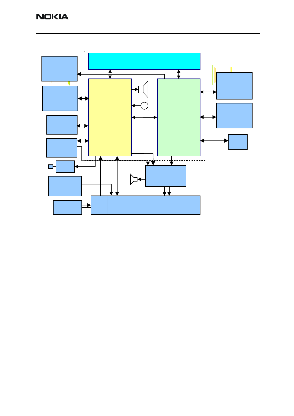
RH-25
T
V
CCS Technical Documentation System Module
LCD
Passive color STN
color display
Led Driver
Keyboard &
display
illumination
ACO RF Module
Combo Memory
64Mbit
Flash/4Mbit SRAM
Keyboard
UEM
Ext Audio
UPP
(UI Module)
Connector
IrDa
Battery
1.8V
ibra
Accessory
Regulator
2.8V 70mA
Charger
jack
Functional Description
Modes of Operation
The RH-25 baseband engine has five different operating modes:
1 No supply
2Acting Dead
3Active
Audio Amp
IHF
DC
Figure 1: RH-25 baseband block diagram
System connector
Tomahawk
4 Sleep
5 Charging
No Supply Mode
In NO_SUPPLY mode, the phone has no supply voltage. This mode is due to the disconnection of main battery or low battery voltage level. The phone will exit from
NO_SUPPLY mode when a sufficient battery voltage level is detected. The battery voltage
Issue 1 10/2003 ©Nokia Corporation Confidential Page 5
Page 6

RH-25
System Module CCS Technical Documentation
can rise either by connecting a new battery with VBAT > VMSTR+, or by connecting
charger and charging the battery voltage to above VMSTR+.
Acting DEAD Mode
If the phone powered off when the charger is connected, the phone is powered on and
enters a state called Acting Dead. In this mode, no RF circuitry is powered up. To the user,
the phone acts as if it is switched off. The phone issues a battery-charging alert and/or
shows a battery charging indication on the display to acknowledge to the user that the
battery is being charged.
Active Mode
In active mode, the phone is in normal operation, scanning for channels, listening to a
base station, transmitting and processing information. There are several sub-states in the
active mode depending on if the phone is in burst reception, burst transmission, etc. In
active mode, SW controls the RF regulators by writing the correct values into the UEM
control registers. VR1A/B can be enabled or disabled. VR2 can be enabled or disabled.
VR4 - VR7 can be enabled, disabled, or forced into low quiescent current mode. VR3 is
always enabled in active mode.
Sleep Mode
The phone enters Sleep mode when both MCU and DSP are in stand-by mode. Both processors control sleep. When the SLEEPX low signal is detected, the UEM enters SLEEP
mode. In this mode, the VCORE, VIO and VFLASH1 regulators are put into low quiescent
current mode. All RF regulators — with the exception of VR2 and VR3 — are disabled in
sleep mode. When the SLEEPX is set high and is detected by the UEM, the phone enters
ACTIVE mode and all functions are activated. Sleep mode is exited either by the expiration of a sleep clock counter in the UEM, or by some external interrupt generated by a
charger connection, key press, or headset connection among other things. While in sleep
mode, the main oscillator is shut down and the baseband section uses the 32 kHz sleep
clock oscillator as its reference.
Charging Mode
Charging can be performed in parallel with any other operating mode. The Battery Size
Indicator (BSI) resistor inside the battery pack indicates the battery type/size. The resistor
value corresponds to a specific battery capacity and technology. The UEM's AD converters, under UPP software control, measure the battery voltage, temperature, size, and current. The charging control circuitry (CHACON) inside the UEM controls the charging
current delivered from the charger to the battery. The battery voltage rise is limited by
turning the UEM switch off when the battery voltage has reached VBATLim (programmable charging cut-off limits 3.6V / 5.0V / 5.25V). Measuring the voltage drop across a
0.22Ohm resistor monitors charging current.
RH-25 BB Functional Blocks
RH-25 BB functional blocks are listed below:
• UEM and UPP
Page 6 ©Nokia Corporation Confidential Issue 1 10/2003
Page 7

RH-25
CCS Technical Documentation System Module
• Battery
• LED Driver
• LCD Display
• RF (TACO) IF Block
• Memory Module
• Keyboard (UI module)
• External Audio Connector
• IrDa Interface
• Vibra
• FM Radio
• System Connector (Tomahawk)
• PWB Strategy
• EMC Strategy
• Test Interface
UEM and UPP
The UEM contains a series of voltage regulators to supply both the baseband module and
the RF module. Both the RF and Baseband modules are supplied with regulated voltages
of 2.78 V and 1.8 V. The UEM contains six linear LDO (low drop-out) regulators for Baseband and seven regulators for RF circuitry. RF regulator VR1 uses two LDOs and a charge
pump. VR1 regulator is used by TACO RF module. The core of the UPP is supplied with a
programmable voltage of 1.0 V, 1.3 V, 1.5 V, or 1.8 V. It should be noted that with UEMK,
VCORE supply voltage is set to 1.5 V. UEMC will support VCORE voltage below 1.5V.
The UPP operates from a 19.44MHz clock generated in the RF ASIC TACO. The DSP and
MCU both contain phase locked loop (PLL) clock multipliers, which can multiply the system frequency by factors from 0.25 to 31. The actual execution speed is limited by the
memory configuration and process size (Max. DSP speed for C035 is ~ 200MHz).
The UEM contains a real-time clock, sliced down from the 32768 Hz crystal oscillator.
The 32768 Hz clock is used by UPP as the sleep clock.
The communication between the UEM and the UPP is done via the bi-directional serial
busses, CBUS and DBus. The CBUS is controlled by the MCU and operates at a speed of
1.08 MHz. The DBus is controlled by the DSP and operates at a speed of 13 MHz. Both
Issue 1 10/2003 ©Nokia Corporation Confidential Page 7
Page 8
RH-25
System Module CCS Technical Documentation
processors are located in the UPP.
The interface between baseband and RF is implemented in the UEM and UPP ASIC. The
UEM provides A/D and D/A conversion of the in-phase and quadrature receive and transmit signal paths. It also provides A/D and D/A conversions of received and transmitted
audio signals to and from the user interface. The UEM supplies the analog signals to RF
section according to the UPP DSP digital control. The RF ASIC, TACO, is controlled via the
UPP RFBUS serial interface. There are also separate signals for PDM coded audio. Digital
speech processing is handled by the DSP inside the UPP ASIC. The UEM is a dual voltage
circuit with the digital parts running from the baseband supply (1.8V) and the analog
parts running from the analog supply of 2.78V. The input battery voltage (VBAT) is also
used directly by some UEM blocks.
The baseband supports both internal and external microphone inputs as well as speaker
outputs. Input and output signal source selection and gain control is done by the UEM
according to control messages from the UPP. Keypad tones, DTMF, and other audio tones
are generated and encoded by the UPP and transmitted to the UEM for decoding. RH-25
has two external serial control interfaces: FBUS and MBUS provided by UEM. These busses can be accessed only through production test patterns.
Battery
RH-25 uses UPP8Mv2.4 and UEMK, with provision to use UEMC and future releases of
UPP as it becomes necessary. UEMC requires some software changes.
BLD-3 Li-ion (inbox battery) is used as main power source for RH-25. No other battery
packs are planned to be used. BLD-3 has the capacity of 780 mAh.
Table 1: BLD-3 characteristics
Description Value
Nominal discharge cut-off voltage 3.1V
Nominal battery voltage 3.7V
Nominal charging voltage 4.2V
Maximum charger output current 850mA
Minimum charger output current 200mA
Cell pack impedance -20 ... 0
Cell pack impedance 0 ... +20
Cell pack impedance +20 ...+60
o
o
C
C
o
C
180mΩ max
150mΩ max
130mΩ max
Cell pack impedance +60 ...+80
o
C
250mΩ max
Page 8 ©Nokia Corporation Confidential Issue 1 10/2003
Page 9
RH-25
CCS Technical Documentation System Module
Table 2: Pin numbering of battery pack
Signal name Pin number Function
VBAT 1 Positive battery terminal
BSI 2 Battery capacity measurement (fixed resistor inside the
battery pack)
BTEMP 3 Battery temperature measurement (measured by ntc
resistor inside pack)
GND 4 Negative/common battery terminal
ge
Char
4(GND)
3(BTEMP)
Figure 2: Battery pack contacts
2(BSI)
GND
The BSI fixed resistor value indicates type and default capacity of a battery. NTC-resistor
measures the battery temperature.
Temperature and capacity information is needed for charge control. These resistors are
connected to BSI and BTEMP pins of battery connector. Phone has 100 kW pull-up resistors for these lines so that they can be read by A/D inputs in the phone. It should be
o
noted that the phone software will shut the phone off if it senses temperature of 38
C or
higher on BTEMP line for safety reasons.
Table 3: BSI resistor values
Parameter Min Typ Max Unit Notes
Battery size indicator resistor BSI 75 kΩ Battery size indicator (BLD-3)
Tolerance “1%
NTC thermistor BTEMP 47
4000
kΩ
K
Battery temperature indicator (NTC pulldown) 47kΩ“5%
o
@ 25
C
Beta value (B).
Tolerance “5%, 25
o
C / 85 oC
Issue 1 10/2003 ©Nokia Corporation Confidential Page 9
Page 10
RH-25
System Module CCS Technical Documentation
VBATT
BTEMP
Supply Voltage Regulation
The UEM ASIC controls supply voltage regulation. There are six separate regulators used
by baseband block. For more detailed description about the regulator parameters see the
document UEM ASIC Specification.
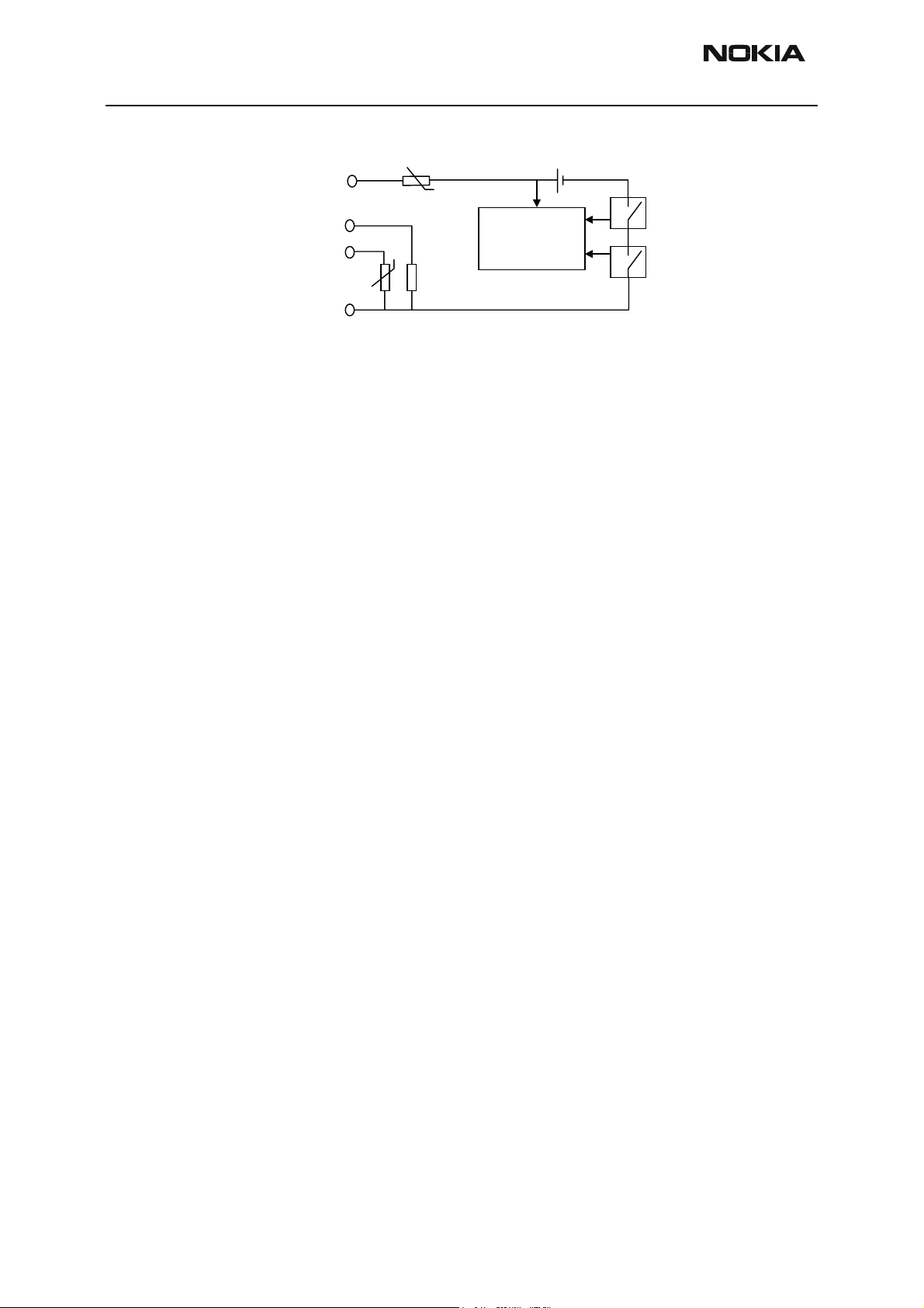
Charging
RH-25 baseband supports the NMP charger interface specified in the document Janette
Charger interface, SW control is specified in EM SW Specification, ISA EM Core SW
Project. The UEM ASIC controls charging, and external components are used to provide
EMC, reverse polarity, and transient protection of the charger input to the baseband
module. The charger connection is through the system connector interface. Both 2- and
3-wire type chargers are supported. The operation of the charging circuit has been specified to limit the power dissipation across the charge switch and to ensure safe operation
in all modes.
BSI
EMC
Figure 3: Interconnection diagram
Li-Ion
Overcharge /
Overdischarge
protection
Page 10 ©Nokia Corporation Confidential Issue 1 10/2003
Page 11
RH-25
V
CCS Technical Documentation System Module
UEM
CHAR
VCHARin
Over
Temp.
Detection
WatchDog
VCHARout
Switch
Driver
Ctrl
Logic
Comp
Vmstr
Current
Sensing/
Limit
+
-
VBATT
VBATTlim
VBATT
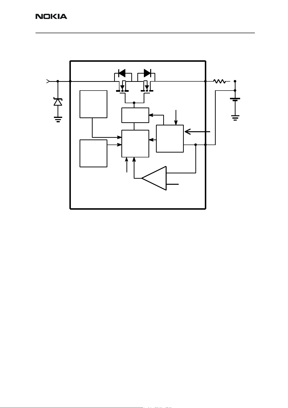
Charger Detection
Connecting a charger creates voltage on the VCHAR input to the UEM. When the VCHAR
input voltage level rises above the VCHDET+ threshold, the UEM starts the charging process. VCHARDET signal is generated to indicate the presence of the charger for the SW.
Energy Management (EM) SW controls the charger identification and acceptance.
The charger recognition is initiated when the EM SW receives a "charger connected"
interrupt. The algorithm basically consists of the following three steps:
1 Check that the charger output (voltage and current) is within safety limits.
2 Identify the charger.
3 Check that the charger is within the charger window.
If the charger is identified and accepted, the appropriate charging algorithm is initiated.
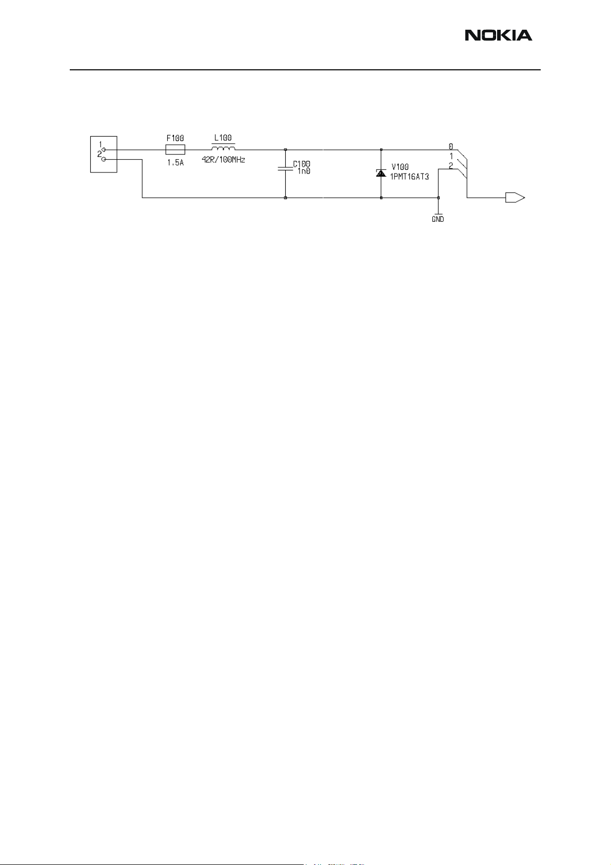
Charger Interface Protection
In order to ensure safe operation with all chargers and in mis-use situations, charger
Figure 4: UEM charging circuitry
Issue 1 10/2003 ©Nokia Corporation Confidential Page 11
Page 12
RH-25
System Module CCS Technical Documentation
interface is protected using transient voltage suppressor (TVS) and 1.5A fuse. The TVS
device used in RH-25 is rated for 16V@175W.
Figure 5: Charger interface TVS characteristics
Breakdown voltage (VBR) 17.8Vmin (at IT 1.0mA)
Reverse standoff voltage (VR) 1 6V
Max reverse leakage current at VR (IR)5uA
Max peak impulse current (Ipp) 7A (at Ta=25*C, current waveform: 10/1000us)
Max clamping voltage at Ipp (Vc) 26V
LED Driver Circuit
In RH-25, white LEDs are used for LCD and keypad lighting. Two LED are used for LCD
lighting and six for keyboard. A step-up DC-DC converter (TK11851) is used as white LED
driver.
The display LEDs are driven in serial mode to achieve stable backlight quality. This means
that constant current flow through LCD LEDs. Serial resistance Rlcd is used to define the
proper current. The feedback signal, FB, is used to control the current. Driver will increase
or decrease the output voltage for LEDs to keep the current stable.
Keyboard LEDs are driven in 2-serial/3 parallel modes. Serial resistance R is used to limit
the current through LEDs. The feedback signal, FB, is not used to control the current.
Driver is controlled by the UEM via DLIGHT output. This signal is connected to driver ENpin (on/off). It is possible to control the LED brightness by PWM to achieve smooth on/off
operation.
Page 12 ©Nokia Corporation Confidential Issue 1 10/2003
Page 13

RH-25
CCS Technical Documentation System Module
VBAT
Cin
DLIGHT
Cosc
Figure 6: Shared LED driver circuit for LCD and keyboard backlight
LCD Backlight
LCD Backlight consists of two white LEDs, which are integrated with the LCD module.
Keyboard Illumination
The keyboard light consists of six white LEDs on the UI board. They are placed under the
keyboard for proper illumination of the keypad.
V in
LED Driver
En
Cx
Coil
Is
Ext
Schottky
Vovp
FB
Gnd
Cout
Rlcd
LCD Illumination
R
Keyboard Illumination
LCD Display
The LCD is a CSTN 130 x 130 full dot matrix display with a color resolution of 12bit
(4096 colors) and a single pixel border area around the content area so the total active
area is 128 x 128 pixels.
LCD parameter Value
Glass size, width x height x thickness 33.98 mm x 37.95 mm x 1.71 mm
Glass thickness 0.50 mm
Viewing area (width x height) 30.29 mm x 30.29 mm
Active pixel area (width x height) 27.29 mm x 27.29 mm
Number of pixels 130 x 130 pixels
Technology CSTN (color super twisted nematic)
Operating temperature range
Main viewing direction 6 o’clock
Illumination mode transflective
Table 4: LCD general specifications
o
-25
C to +70 oC
Color tone
Background: Neutral/Black
Issue 1 10/2003 ©Nokia Corporation Confidential Page 13
Page 14

RH-25
A
System Module CCS Technical Documentation
C
Driver
Top View
ctive area
128x128
C C
C 0 C 128
R 0
R 128
Figure 7: Color LCD module
RF Interface Block
The interface between the baseband and the TACO RF module can be divided into two
categories. The first is the digital interface. It interfaces between the UPP and the RF
chip. The serial digital interface is used to control the operation of the different blocks in
the RF chip. The second is the analog interface. It interfaces between the UEM and the
RF. The entire BB-RF interface is discussed in RF-BB Interface Specification RH-25 .
Combo Memory Module
The RH-25 baseband memory module consists of a combo Flash/SRAM chip. It has
64Mbit burst-type flash memory and 4-Mbit of SRAM. In addition, the UPP has 8Mbit of
internal RAM. The UPP RAM is part of UPP and is not covered here.
Combo Memory Interface
The memory interface consists of multiplexed address/data bus MEMADDA [23:0], the
MEMCONT[9:0] memory control bus, and GENIO[23] — which is used for memory control.
The purpose of the memory interface is to reduce the amount of interconnections by
multiplexing the address and data signals on the same bus. Since the required flash
address space is more than 16-bits, the MEMADDA[15:0] are multiplexed address/data
lines and MEMADDA[21:16] are only address lines, which in total allow for 4M addresses
(MEMADDA[21:0]). The multiplexed data/address lines require the memory to store the
address during the first cycle in the read/write access. Data access to the flash is performed as a 16-bit access (MEMADDA[15:0]) in order to improve the data rate on the
bus. The memory interface supports asynchronous read, burst mode synchronous read,
and simultaneous read-while-write/erase — all controlled by the UPP.
SRAM Memory Description
The combo memory chip used in RH-25 has 4 Mbit of SRAM, 16-bits wide running at
1.8V. It uses multiplexed address and data bus to minimize the pin count of the device.
Control signals are used to allow byte access to the device.
Flash Memory Description
The 64 Mbit density flash with 16-bit data access operates in both asynchronous random
Page 14 ©Nokia Corporation Confidential Issue 1 10/2003
Page 15

RH-25
CCS Technical Documentation System Module
access and synchronous burst access (with crossing partition boundaries) and has various
data protection features. Upon power up or reset, the device defaults to asynchronous
read configuration. Synchronous burst read is indicated to the device by writing to the
flash configuration register and can be terminated by deactivating the device.
The device supports reads and in-system erase and program operations at Vcc=1.8 V
(Voltage range 1.7-1.9 V). Flashing at production is supported at Vpp=12 V (for limited
exposure length only).
Flash Architecture
Datasheet of RH-25 combo memory contains detailed information about Flash architecture.
Keyboard (UI Module)
RH-25 consists of separate UI board, includes contacts for the keypad domes and LEDs
for keypad lighting. UI board is connected to the main PWB through 16 pole board-toboard connector with springs. A 5x4-matrix keyboard is used in RH-25. Key pressing is
detected by scanning procedure. Keypad signals are connected, UPP keyboard interface.
When no key is pressed, row inputs are high due to UPP internal pull-up resistors. The
columns are written zero. When key is pressed, one row is pulled down and an interrupt
is generated to MCU. After receiving interrupt, MCU starts scanning procedure. All columns are first written high and then one column at the time is written down. All other
columns except one, which was written down, are set as inputs. Rows are read while column at the time is written down. If some row is down it indicates that key which is at
the cross point of selected column and row was pressed. After detecting pressed key all
registers inside the UPP are reset and columns are written back to zero.
Keyboard ESD Protection
SMD chips LEDs on UI board have 2kV ESD protection. In case the A-cover is removed,
there is a potential risk of damaging LEDs with electrostatic discharge. Ground openings
are made around LEDs to catch ESD sparks. For additional protection, dome sheet is
made of conductive metallized tape and grounded to display shield.
Internal Audio
Internal Microphone
The internal microphone capsule is mounted to in the UI frame. Microphone is omni
directional and it's connected to the UEM microphone input MIC1P/N. The microphone
input is asymmetric and the UEM (MICB1) provides bias voltage. The microphone input
on the UEM is ESD protected. Spring contacts are used to connect the microphone to the
main PWB.
Issue 1 10/2003 ©Nokia Corporation Confidential Page 15
Page 16

RH-25
System Module CCS Technical Documentation
ge
Char
UEM
MIC1N
Internal Speaker
The internal earpiece is a dynamic earpiece with impedance of 32 ohms. The earpiece is
low impedance one since the sound pressure is to be generated using current and not
voltage as the supply voltage is restricted to 2.7V. The earpiece is driven directly by the
UEM and the earpiece driver (EARP and EARN outputs) is a fully differential bridge
amplifier with 6 dB gain. In RH-25, 8mm leak tolerant PICO earpiece is used.
UEM
MIC1P
EARP
EARN
EMC
Microphone
Figure 8: Internal microphone connection
Common mode
choke
Figure 9: Speaker connection
IHF Speaker and Stereo Audio Amplifier
Integrated Hands Free Speaker (16mm MALT) is used to generate speech audio, ringing
and warning tones in RH-25. Audio amplifier is controlled by the UPP. Speaker capsule is
mounted in the C-cover. Spring contacts are used to connect the IHF Speaker contacts to
the main PWB.
Page 16 ©Nokia Corporation Confidential Issue 1 10/2003
Page 17

RH-25
CCS Technical Documentation System Module
Phone
audio
By pass
UPP8M
GenIO(14)
GenIO(15)
GenIO(16)
Enable
Clock
Data
Figure 10: Digital interface of audio amplifer
VB AT
=
LM4855
Output
Mode
Select
SPI
Ri n
Li n
Bias
Amplifier
Amplifier
Amplifier
Digital
Volu me
Control
LM4855
EN
CLK
DATA
Amplifier
Amplifier
Amplifier
GN D
ou t +
ou t -
Rout +
Rout -
Lout +
Lout -
Stereo
IH F Speaker
Headset
The LM4855 features a 32-step digital volume control and eight distinct output modes.
The digital volume control and output modes are accessed through a 3-wire interface,
controlled by UPP. Digital volume control is needed when FM radio is activated; there is
no amplifier block in FM radio module. Output modes are needed when routing audios to
different locations; Headset or IHF.
External Audio Connector
RH-25 is designed to support fully differential external audio accessory connection by
using Tomahawk system connector. Tomahawk connector has serial data bus called (ACI)
Accessory Control Interface (ACI) for accessory insertion and removal detection and
identification and authentication. ACI line is also used for accessory control purposes.
• 4-wire fully differential stereo audio (used also FM-radio antenna connection)
• 2-wire differential mic input
EN CL K DAT A
Figure 11: Block diagram of audio amplifer
Issue 1 10/2003 ©Nokia Corporation Confidential Page 17
Page 18

RH-25
Ct
A
System Module CCS Technical Documentation
External Microphone Connection
The external microphone input is fully differential and lines are connected to the UEM
microphone input MIC2P/N. The UEM (MICB2) provides bias voltage. Microphone input
lines are ESD protected.
Creating a short circuit between the headset microphone signals generates the hook signal. When the accessory is not connected, the UEM resistor pulls up the HookInt signal.
When the accessory is inserted and the microphone path is biased the HookInt signal
decreases to 1.8V due to the microphone bias current flowing through the resistor. When
the button is pressed the microphone signals are connected together, and the HookInt
input will get half of micbias dc value 1.1 V. This change in DC level will cause the HookInt comparator output to change state, in this case from 0 to 1. The button can be used
for answering incoming calls but not to initiate outgoing calls.
HookInt
MICB2
UEM
MIC2P
MIC2N
Figure 12: External microphone connection
External Earphone Connection
Headset implementation uses separate microphone and earpiece signals. The accessory is
detected by the HeadInt signal when the plug is inserted.
FM Radio
VAFR
VAFL
MIC3P
UEM
MIC3N
XEAR
udio Amplifier
Rin
Lin
PhoneIN (HS)
PhoneIN (IHF)
Rout+
RoutLout+
Lout-
SPKRout+
SPKRout
XMICP
EMC/ESD
XMICN
EMC/ESD
-
IHF Speaker
Figure 13: External earphone and IHF connections
Page 18 ©Nokia Corporation Confidential Issue 1 10/2003
Page 19

RH-25
CCS Technical Documentation System Module
IrDa Interface
The IrDa interface when using transceiver with 1.8V I/O is designed into the UPP. The IR
link supports speeds from 9600 bit/s to 1.152 MBit/s up to distance of 80 cm. Transmission over the IR if half-duplex.
The length of the transmitted IR pulse depends on the speed of the transmission. When
230.4 kbit/s or less is used as a transmission speed, pulse length is maximum 1.63ms. If
transmission speed is set to 1.152Mbit/s, the pulse length is 154ns.
IR transceiver can be set into SIR or MIR modes. In SIR mode transceiver is capable of
transmission speed up to 115.2kbit/s. In MIR mode faster transmission speeds are used.
The maximum speed is 1.152Mbit/s. IR transceiver can be set into shutdown mode by
setting SD pin to logic '1' for current saving reasons.
Vibra
A vibra alerting device is used to generate a vibration signal for an incoming call. Vibra is
located in the bottom end of the phone and connection is done with spring contacts.
Vibra interface is the same like other DCT4 projects. The vibra is controlled by a PWM
signal from the UEM. Frequency can be set to 64, 129, 258, or 520 Hz and duty cycle can
vary between 3% - 97%. To ensure compatibility with different version of UEM, RH-25
uses 40.5% duty cycle of the vibra PWM signal.
FM Radio
FM radio circuitry is implemented by using highly integrated radio IC, TEA5767. TEA5767
is a single-chip, electronically tuned FM stereo radio with fully integrated IF selectivity
and demodulation. The IF-frequency is 225 kHz. The radio is completely adjustment-free
and does only require a minimum of small and low-cost external components. It has signal-dependent mono/stereo blend [Stereo Noise Cancelling (SNC)]. The radio can tune
the European, US, and Japan FM bands. This will be offered as an accessory with
RH-25.
Channel tuning and other controls are controlled through serial bus interface by the
MCUSW. Reference clock, 32kHz, is generated by the UPP CTSI block (routed from sleep
clock).
GenIO(3)
UPP8M
GenIO(12)
GenIO(11)
GenIO(8)
FMCtrlDa
FMCtrlClk
FMWrEn
FMClk
VIO
XTAL2
TEA5767
SDA
SCL
W/R
Figure 14: FM radio digital interface connections
Issue 1 10/2003 ©Nokia Corporation Confidential Page 19
Page 20

RH-25
N
System Module CCS Technical Documentation
System Connector (Tomahawk)
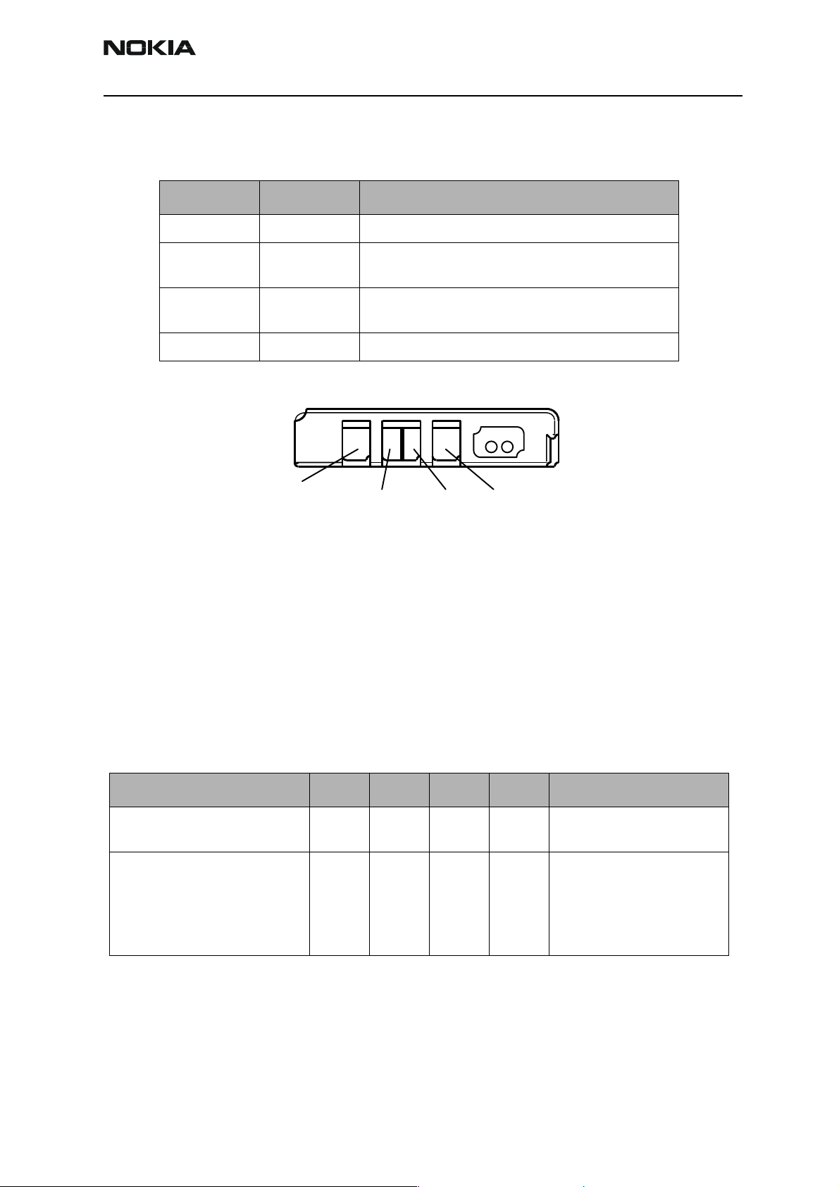
The 14-pin Tomahawk bottom connector consists of charging plug socket and Tomahawk
System Connector. Tomahawk system connector includes signals for the following:
Table 5: Tomahawk system connector signals
Function Notes
Charging Pads for 2-wire charging in cradles
Audio 4-wire fully differential stereo audio output
2-wire differential microphone input
FM radio antenna connection
Power supply for accessories 2.78V/70mA output to accessories
ACI (Accessory Control Interface) Accessory detection/removal and controlling
FBUS Standard FBUS
DKU-5 (similar to USB) (optional) Power in 5V in from DKU-5 cable
ACI
Vout
Charge
Charge GND
Shielding GND
Fbus TX
Fbus RX
XMIC N
XMIC P
DATA GND
HSEAR_L_P
HSEAR_L_N
Figure 15: Tomahawk bottom connector (charger plug socket and Tomahawk system connector)
Accessory Control Interface (ACI)
ACI is point-to-point, bi-directional serial bus. It has three main features:
1 The insertion and removal detection of an accessory device
2 Acting as a data bus, intended mainly for control purposes
3 The identification and authentication of accessory type which is connected
The accessories are detected by the HeadInt signal when the plug is inserted. Normally
when accessory is not present, the pull-up resistor 100k pulls up the HeadInt signal to
VFLASH1. If the accessory is inserted, the external resistor (located to accessory) works
as voltage divider and decreases the voltage level below the threshold of Vhead. Thereby
the comparator output will be changed to high state causing an interrupt.
HSEAR_R_N
HSEAR_R_P
Shielding GND
If the accessory is removed, the voltage level of HeadInt increases again to VFLASH1.This
Page 20 ©Nokia Corporation Confidential Issue 1 10/2003
Page 21

RH-25
3985
CCS Technical Documentation System Module
voltage level is higher than the threshold of the comparator and thereby its output will
be changed to low. This changes is leading to an interrupt. These HeadInt interrupts are
initiated the accessory detection or removal sequence.
External Accessory Regulator
An external LDO Regulator is needed for accessory power supply purposes. All ACI-accessories will require this power supply. Regulator input is connected to battery voltage
VBAT and output is connected to Vout pin in Tomahawk connector. Regulator ON/OFF
function is controlled via UPP.
The pull-down resistor on the enable input of the regulator is needed because in the
switch-off mode of the phone, the output level of the Genio(0) is not defined. If Genio(0)
is floating, the regulator may be enabled when it shouldn't be.
UPP
GenIO(0)
PWB Strategy
PWB Construction
The PWB in RH-25 consists of a 6-layer board made up of FR4.
Via types are through hole, laser, buried, and blind vias.
The PWB build up is shown below:
VBAT
Voltage
En
regulator
LP
Figure 16: Accessory power supply diagram
Tomahawk btm conn
VOUT
Issue 1 10/2003 ©Nokia Corporation Confidential Page 21
Page 22

RH-25
System Module CCS Technical Documentation
Solder resist 20 µm ± 10 µm
±
110
Maximum thi ckness with solder resist 1270um
Electromechanical Thi ckn ess with surface finish 1100um
Finished copper 30 µm ± 10 µm
Dielectric Aramid 100 µm ± 20 µm
Finished copper 17 µm +2/-5 µm
Dielectric 150 µm ± 25 µm
Finished copper 17 µm +2/-5 µm
Dielectric 150 µm ± 25 µm
Finished copper 17 µm +2/-5 µm
Dielectric 150 µm ± 25 µm
Finished copper 17 µm +2/-5 µm
Dielectric Aramid 100 µm ± 20 µm
Finished copper 30 µm ±10 µm
Solder resist 20 µm ± 10 µm
PWB Immunity
The PWB has been designed to shield all lines susceptible for radiation. Sensitive PWB
tracks have been drawn with respect to shielding by having ground plane over tracks,
and ground close to the tracks at the same layer.
All edges are grounded from both sides of PWB and solder mask is opened from these
areas. Target is that any ESD pulse faces ground area when entering the phone; for
example, between mechanics covers. All holes in PWB are grounded and plated through
holes.
Keyboard
The keyboard PWB layout consists of a grounded outer ring and either a trefoil pattern
grid (matrix) or an inner pad. This construction makes the keys immune for ESD, as the
keydome will have a low ohmic contact with the PWB ground.
Audio Lines
In order to obtain good signa-to-noise ratio and good EMC/ESD immunity, the audio
lines have been carefully routed with respect to obtaining low impedance in the signal
path and obtaining proper shielding.
Figure 17: RH-25 PWB build up
Microphone Lines
Microphone signals are input lines and therefore very sensitive to radiated fields. Immunity for radiated fields is done to obtain a low-impedance path and with respect to a
common noise point of view in the signal path. This is applied for both internal and
external microphone lines.
Page 22 ©Nokia Corporation Confidential Issue 1 10/2003
Page 23

RH-25
CCS Technical Documentation System Module
EAR Lines
EAR lines are output signals, also routed on layer 2 and 7, to obtain immunity for conducted emission from UEM. Internal EAR lines are EMC/ESD protected by radiated fields
from the earpiece by the low-impedance signal path in the PWB.
The same PWB outline has been implemented for the SALT speaker. Low ohm coils inductors are used in series with the speaker for immunity against incoming fields from the
speaker.
Charger Lines
Ground from the charger is connected directly to common PWB ground for low impedance path to the battery. The positive charger line will be ESD, EMC, and short-circuit
protected by appropriate circuits.
HEADINT
This line is EMC/ESD protected by routing on shielded layer 2 and by placement of resistor R154 close to the bottom connector.
Battery Supply Filtering
Battery supply lines to the UEM IC are filtered with LC filter. These filters provide immunity against conducted RF noise
System Connector
The immunity strategy concerning the bottom connector lines is to shield all lines to this
part in order to prevent radiation in the phone itself when external accessory is connected and to prevent radiated fields from disturbing the lines as well. Appropriate discrete filters close to the bottom connector are implemented for EMC and ESD protection.
Mechanical Shielding
RH-25 has metal shield over RF parts and BB parts to provide immunity for internal radiation and immunity for external fields.
EMC Strategy
The RH-25 phone must comply with the given CE requirements concerning EMC and ESD.
The goal is to pass internal SPR requirements. Therefore attention has been paid to
obtaining immunity in the PWB layout itself, and the implementation of filters in the circuit design.
Requirements for EMC and ESD:
• CE requirements for EMC and ESD according to ETS 300 342-1
• Internal requirements for EMC and ESD are according to SPR4
The baseband EMC strategy is divided into electrical and mechanical items. All electrical
guide lines, clocks, and high-speed signals should be routed in inner layers and away
from the PWB edges. Clock signals distributed to other circuits should have series resis-
Issue 1 10/2003 ©Nokia Corporation Confidential Page 23
Page 24

RH-25
System Module CCS Technical Documentation
tors incorporated to reduce rise times and reflections. Slew rate controlled buffers should
be used on custom components wherever possible to reduce the EMC produced by the
circuit. Separate power supplies for digital, analog, and RF-blocks should be used as
much as possible. Baseband and RF supply power rails should be isolated from each other
by means of inductors in the power supply rail to prevent high-frequency components
produced on the baseband power supply rail to spread out over the RF power supply
plane. This might be required to avoid interference from digital circuits to affect the performance of RF section.
All external connectors and connection must be filtered using RC or LC networks to prevent the high frequency components from entering connection cables that then will act
as antennas. The amount of this type of EMC component is in straight relation to the
amount of external connections. The type of network and amount of components to be
used is determined by the AC and DC impedance characteristic of that particular signal.
Low-impedance signals require LC networks while medium impedance level signals
(input signals at moderate bandwidth) can use RC networks.
The EMC protection should also prevent external or internal signals to cause interference
to baseband and in particular to audio signals. Internal interference is generated by the
transmitter burst frequency and the switchmode charging. The transmitter burst frequency interference is likely to cause noise to both microphone and earphone signals.
The transmitter RF interference is likely to cause more problems in the microphone circuitry than in the earphone circuitry since the earpiece is a low impedance dynamic type.
As mechanical guidelines, the baseband and RF sections should be isolated from each
other using EMC shielding, which suppresses radiated interference. The transmitter burst
frequency can also generate mechanical vibrations that can be picked up by the microphone if it is not properly isolated from the chassis using rubber or some other soft
material. Connection wires to internal microphone and earphone should be as short as
possible to reduce the interference caused by internal signals.
ESD protection has to be implemented on each external connection that is accessible
during normal operation of the phone.
Test Interfaces
Using the Tomahawk connector FBUS connections, the phone HW can be tested by PC
software (i.e., Phoenix test software). In addition, RH-25 will also support Flash programming interface via the service battery, JTAG, and Ostrich test interfaces. JTAG test interface may be removed from the final product for security reasons.
Production / After Sales Interface
Test pads are placed on engine PWB, for service and production purposes. Same test pattern is used by the After Market Sales (AMS) group for product testing and software
upgrades. The following figure shows the top view of the test pads. FBUS_TX and RX
lines are used to transfer data in or out of the phone. VPP is the Flash programming voltage and MBUS/CLK line is used as Flash clock line during flashing of phone.
Page 24 ©Nokia Corporation Confidential Issue 1 10/2003
Page 25

RH-25
CCS Technical Documentation System Module
Flash Interface
Flash programming in production is done through the test pads in the above figure on
the PWB.
FBUS Interface
FBUS is an asynchronous data bus having separate TX and RX signals. Default bit rate of
the bus is 115.2 kbit/s. FBUS is mainly used for controlling and programming phone in
the production. This is the primary interface used in RH-25.
FBUS_RX FBUS_TX
VPP
MBUS/CLK
Figure 18: Production/test/after market interface
GND
Issue 1 10/2003 ©Nokia Corporation Confidential Page 25
Page 26

RH-25
System Module CCS Technical Documentation
BB_RF Interface Connections
The BB and RF parts are connected together without a physical connector.
Rip
Signal
Name
#
DAMPS,
GSM1900
RFICCNTRL(2:0) RF IC Control Bus from UPP to RF IC (TACO)
RFBUSCLK UPP RFIC In Dig
0
RFBUSDA UPP/RFIC RFIC
1
RFBUSEN1X UPP RFIC In Dig
2
PUSL(2:0) Power Up Reset from UEM to RF IC (TACO)
PURX UEM RFIC Out Dig
0
GENIO(28:0) General I/O Bus connected to RF, see also separa te collective GENIO(28:0)
TXP1 RFIC UPP Out Dig
5
Connected
from--- to
UPP
BB
I/O
Signal Properties
A/D--Levels---Freq./
Timing resolution
0/1.8V
I/O Dig
(0: <0.4V
9.72 MHz RF Control serial bus bit clock
Bi-directional RF Control serial bus data,
1: >1.4 V)
RFIC Chip Sel X
0/1.8V 10us Power Up Reset for RF IC
SLCLK & SLEEPX not used in RF
table. Control lines from UPP GENIOs to RF
0/1.8V
10 us Low Band Tx enabled
Description / Notes
6
11
TXP2 RFIC
BANDSEL
RFIC
UPP Out Dig
UPP Out Dig
0/1.8V
0/1.8V
High Band Tx enabled
Rx Band select. Option for module LNA.
Not used in Stella.
Page 26 ©Nokia Corporation Confidential Issue 1 10/2003
Page 27

RH-25
CCS Technical Documentation System Module
Rip
Signal
Name
#
DAMPS ,
GSM1900
RFCLK (not BUS -> no rip #) System Clock From RF To BB, original source VCTCXO, buffered (and
RFCLK
Connected
from--- to
VCTCXO >
RFIC
BB
I/O
Signal Properties
A/D--Levels---Freq./
Timing resolution
frequency shifted, WAM only) in RF IC (TACO)
UPP In Ana 800mVpp
typ (FET
probed)
Bias DC
blocked at
UPP input
Description / Notes
19.44 MHz System Clk from RF to BB,
RFClk
GND
SLOWAD(6:0) Slow Speed ADC Lines from RF block
5 PDMID
6 PATEMP
RF UPP In Ana 0 System Clock slicer Ref GND, not
separated from pwb GND layer
RF Power
detection
module
RF Power
detection
module
UEM In
UEM In
Ana
0/2.7V dig 0/VR2 Power detection module identification to
slow ADC (ch 5, previous VCTCXO Temp)
signal to UEM.
Ana
0.1-2.7V - Tx PA Temperature signal to UEM, NTC in
Power Detection Module
RFCONV(9:0) RF- BB differential Analog Signals: Tx I&Q, Rx I&Q and reference voltage
0
1
2
3
4
5
6
7
9
RXIP
RXIN
RXQP
RXQN
TXIP
TXIN
TXQP
TXQN
VREFRFO1
RFIC UEM In
UEM RFIC Out
UEM RFIC Out
Ana
Ana
Vref
1.4Vpp
max. diff.
Differential positive/negative in-phase Rx
Signal
0.5Vpp typ
bias
1.30V
2.2Vpp
max. diff.
Diff. Positive/negat ive quadrature phase Rx
Signal
Differential positive/ ne gative in-phase Tx
Signal
0.6VppTyp
Bias
1.30V
Differential positive/ ne gative quadrature
phase Tx Signal
1.35 V RF IC Reference voltage from UEM
Rip
#
Signal
Name
DAMPS,
GSM1900
Connected
from--- to
BB
I/O
Signal Properties
A/D--Levels---Freq./
Timing resolution
Description / Notes
RFAUXCONV(2:0) RF_BB Analog Control Signals to/from UEM
TXPWRDET
1
AFC
2
TXP Det. UEM In Ana
UEM VCTCXO Out Ana
0.1-2.4 V 50 us Tx PWR Detector Signal to UEM
0.1-2.4 V Automatic Frequency Control for VCTCXO
Issue 1 10/2003 ©Nokia Corporation Confidential Page 27
Page 28

RH-25
System Module CCS Technical Documentation
RF
V
Globals instead of Bus Regulated RF Supply Voltages from UEM to RF. Current values are of the
VR1 A UEM RFIC
VR1 B UEM RFIC
VR2 UEM RFDiscr./
RFIC
VR3 UEM VCTCXO
VR4 UEM RFIC
VR5 UEM RFIC
VR6 UEM RFIC
VR7 UEM RFIC,
UHF VCO
IPA1 UEM RF PA
IPA2 UEM RFPA
VFLASH1 UEM RFIC
VBATT, Global
VBATTRF Batt
RFPA
Conn
regulator specifications, not the measured values of RF
Out Vreg
Out Vreg
Out Vreg
Out Vreg
Out Vreg
4.75 V
+- 3 %
4.75 V
+- 3 %
2.78 V
+- 3 %
2.78 V
+- 3 %
10 mA max. UEM, charge pump + linear regulator
output. Supply for UHF synth phase det ….
10 mA max. UEM, charge pump + linear regulator
output.
100 mA max. UEM linear regulator. Supply voltage for Tx
IQ filter and IQ to Tx IF mixer.
20 mA max. UEM linear regul ator. Supply for VCTCXO +
RFCLK Buffer in RF IC.
--”-- 50 mA max. UEM linear regulator. Power Supply for LNA
/ RFIC Rx chain.
Out Vreg
--”-- 50 mA max. UEM linear regulator. P ower Supply for RF
low band PA driver section.
Out Vreg
--”-- 50 mA max. UEM linear regulator. P ower supply for RF
high band PA driver section.
Out Vreg
--”-- 45mA UEM linear regulator. Power supply for RF
Synths
Out Iout
Out Iout
Out Iout
0-5 mA Settable Bias current for RF PA L-Band
0-5 mA Settable Bias current for RF PA H-band
2.78V ~2mA UE M linear regul ator common for BB.
RFIC digital parts and RF to BB digi IF.
Out Vbatt
3…5V 0…1A
Raw Vbatt for RF PA
2A peak
Page 28 ©Nokia Corporation Confidential Issue 1 10/2003
Page 29

RH-25
CCS Technical Documentation System Module
RF Functional Description
Block diagram
VBatt
RFRegs
RFConv
4.7VB
4.7V
VR 6
VR 7
IPA1& 2
VR 2
VR 3
VR 4
VR 5
2.78V
2.78V
2.78V
2.78V
2.78V
2.78V
0...5mA
2.78V
A
VR 1
VR 1
VFlash1
RFAuxConv
RH-25 RF
-20dB @
+-60kHz
f
O
+8dB
VR 4
+8dB
VR 4
135.54MHz IF Filters
DIV 2
VR 7
VR 7
UHF
VCO
VR 7
2
+5dBm
2
+6dBm
2
TDMA
TDMA
222
Rx
VCO
VR 7
PHASE
DET.
VR 7
VR 1 A
PHASE
DET.
PHASE
DET.
Tx
VCO
VR 1B
VR 2
VR2
Presc.
VR 7
VR 7
180.54MHz
VFLASF1/VR7
VHF - PLL
Rx
271. 08 M H z
UHF - PLL
2008. ..2125 MH z
VHF - PL L Tx
361.08 MHz
VR 7
2
I & Q fixed
Gain +24dB
VR 4
VFLASF1/V R7
VFLASF1/VR7
2
I & Q va ri ab l e G ain
-6 ... +36dB
fL=14k TDMA
7 steps of 6d B
+18dB 4th Chbv -6 ... +36dB
VR 4
VR 4
2X D AC
8 bit
DIV 2
OFFSET
CONTR.
VR 4
VR 4
VR4
VRe f1
I
VR 4 VR 4
VR4
Q
VR 4VR 4
VFlash1
CONTROL
REGS
GEN I/O
Serial IF
PURX
CLK
DAT A
ENA
VR3
VIO
VR 3
VCTCXO
19.44 MHz
AFC
I
VR2
VR2
DIV 2
VR2
VR2
-44 ... +1 2dB
step 4dB
VR2
2
TXP1
TXP2
TXP1
Q
VR2
0 ... 5mA
RF
ANT
+28dBm
@Tx lvl2
VBatt
IPA1
VBatt
+16/-4dB
@U
RF
IPA2
</>70dBm
RX
TX
L
VR5
TDMA Low:
869.01 ... 893.97
LNAL
VR 4
BIAS
CONT
VR 4
2
2
(V R 3)
LNAH
+1 5/ 0d B
RX
HIGH
BAND
TX
LOW
BAND
H
H
DET.
L
-T
VR2
VR6
+30dBm
PDMid
TXPWRDet
PATemp
+30dBm
PURX
Figure 19: Block diagram of the RH-25 RF module
Issue 1 10/2003 ©Nokia Corporation Confidential Page 29
Page 30

RH-25
System Module CCS Technical Documentation
As the previous figure clearly shows, most of the RF functions are centered around Taco
RF ASIC. Receiver IF stages, low-band LNA, PLLs, RXVHF oscillator, TX VHF VCO active
part and loop filter, high-band and low-band TX up-converters, TX IF stages, IQ modulator and demodulator and reference oscillator buffering are all integrated on single chip.
Taco design and sample testing are carried out by ASIC team. Application responsibility
lies on RF design team as well as the components outside Taco. Externally sourced key
components are:
• 19.44 MHz VCTCXO
• 2 GHz UHF VCO
• 800MHz PA
• 1900MHz PA
• Power detector module
• 1900MHz LNA transistor
• Duplexer low band
• Duplexer high band
• RX800, RX1900, TX800, and TX1900 SAWs
• RX IF and TX IF Filters
The specifications for all key components are maintained by RF team and are available in
network.
Circuit Diagrams and PWB Layout
Receiver
Receiver design and system partition come from Snoopy AD project. The receiver shows a
superheterodyne structure with zero 2nd IF. Low-band and high- band receivers have
separate front ends from diplexer to the 1st IF. Most of the receiver functions are integrated in RF ASIC. The only functions out of the chip are high-band LNA, duplexers, and
SAW filters. In spite of a bit different component selection, receiver characteristics are
very similar on both bands.
An active 1st down-converter sets naturally high gain requirements for preceding stages.
Hence, losses in very selective front end filters are minimized down to the limits set by
filter technologies used and component sizes. LNA gain is set up to 16dB, which is close
to the maximum available stable gain from a single-stage amplifier. LNAs are not exactly
noise matched in order to keep pass band gain ripple in minimum. Filters have relative
tight stop band requirements, which are not all set by the system requirements but the
interference free operation in the field. In this receiver structure, linearity lies heavily on
Page 30 ©Nokia Corporation Confidential Issue 1 10/2003
Page 31

RH-25
CCS Technical Documentation System Module
mixer design. The 2nd order distortion requirements of the mixer are set by the 'half IF'
suppression. A fully balanced mixer topology is required. Additionally, the receiver 3rd
order IIP tends to depend on active mixer IIP3 linearity due to pretty high LNA gain.
IF stages include a narrowband SAW filter on the 1st IF and an integrated lowpass filtering is on zero IF. SAW filter guarantees 14dBc attenuation at alternating channels, which
gives acceptable receiver IMD performance with only moderate VHF local phase noise
performance. The local signal's partition to receiver selectivity and IMD depends then
mainly on the spectral purity of the 1st local. Zero 2nd IF stages include most of receivers signal gain, AGC control range and channel filtering.
Receiver requirements and characteristics are presented in detail in RX specification.
Frequency Synthesizers
RH-25 synthesizer consists of three synthesizers: one UHF synthesizer and two VHF synthesizers. UHF synthesizer is based on integrated PLL and external UHF VCO, loop filter,
and VCTCXO. It main goal is to achieve the channel selection, thus for dual band operations associated with dual mode. Due to the RX and TX architecture, this UHF synthesizer
is used for down conversion of the received signal and for final up-conversion in transmitter. A common 2GHz UHFVCO module is used for operation on both low and high
band. Frequency divider by two is integrated in Taco.
Two VHF synthesizers consist of: RX VHF Synthesizer includes integrated PLL and VCO
and loop filter and resonator. The output of RX-VHF PLL is used as LO signal for the second mixer in receiver. TX VHF Synthesizer and Loop filter is integrated into the Taco. See
depicted block diagrams and synthesizer characteristics from Synthesizer specification
document.
Transmitter
The transmitter RF architecture is up-conversion type (desired RF spectrum is low side
injection) with (RF-) modulation and gain control at IF. The IF frequency is 180.54MHz.
The cellular band is 824.01-848.97MHz and PCS band is 1850.01-1909.95MHz.
Common IF
The RF modulator is integrated with Programmable Gain Amplifier (PGA) and IF output
buffer inside Taco RFIC-chip. I- and Q-signals, that are output signals from BB-side SW
IQ-modulator, have some filtering inside Taco before RF modulation is performed. The
required LO-signal from TXVCO is buffered with phase shifting in Taco. After modulation
(p/4 DQPSK or FM), the modulated IF signal is amplified in PGA.
Cellular Band
At operation in cellular band, the IF signal is buffered at IF output stage that is enabled
by TXP1 TX control. The maximum linear (balanced) IF signal level to 50W load is about 8 dBm.
For proper AMPS-mode receiver (duplex) sensitivity, IF signal is filtered in strip-filter
before up-conversion. The upconverter mixer is actually a mixer with LO and output
driver being able to deliver about +6dBm linear output power. Mixer is inside Taco RF IC.
Issue 1 10/2003 ©Nokia Corporation Confidential Page 31
Page 32

RH-25
System Module CCS Technical Documentation
Note, that in this point, term linear means -33dB ACP. The required LO power is about
-6dBm. The LO signal is fed from Taco.
Before power amplifier RF signal is filter in band filter. The typical insertion loss is about
-2.7dB, and maximum less than -3.0dB. The input and output return losses are about
-10dB.
Power amplifier is 50W/50W module. It does not have own enable/disable control signal,
but it can be enabled by bias voltage and reference bias current signals. The gain window
is +27 to +31dB and linear output power is +30dBm (typical condition) with -28dB ACP.
The nominal efficiency is 50%.
PCS Band
At operation in PCS band, the IF signal is routed outside from Taco to be filtered in TX IF
strip filter, and after that back to Taco, to the up-converter mixer. The LO-signal to the
mixer is buffered and balanced inside Taco. The mixer output is enabled by TXP2 TX control signal. The maximum linear (balanced) RF signal level to 50W load is about +7dBm.
After Taco balanced RF-signal is single-ended in 1:1 balun and then filtered in SAW filter. The typical insertion loss is about -4.0dB, and maximum less than -5.0dB. This filter
hasrelatively high pass band ripple about 1.0-1.5dB, largest insertion being at high end
of the band. The input and return losses are about -10dB.
Power amplifier is 50W/50W module. It does not have own enable/disable control signal,
but it can be enabled by bias voltage and reference bias current signals. The gain window
is +31 to +36dB and linear output power is +30dBm (typical condition) with -28dB ACP.
The nominal efficiency is 40%.
Power Control
For power monitoring, there is a power detector module (PDM) build up from a (dual)
coupler, a biased diode detector and an NTC resistor. RF signals from both bands are
routed via this PDM. The RF isolation between couplers is sufficient not to loose filtering
performance given by duplex filters.
The diode output voltage and NTC voltage are routed to BB A/D converters for power
control purpose. The TX AGC SW takes samples from diode output voltage and compares
that value to target value, and adjust BB I-and Q-signal amplitude and/or Taco PGA settings to keep power control in balance.
NTC voltage is used for diode temperature compensation and for thermal shut down
when radio board's temperature exceeds +85°C.
False TX indication is based on detected power measurement when carrier is not on.
The insertion loss of coupler is -0.42dB (max) at cellular band and -0.48dB (max) at PCS
band. Typical values for insertion losses are about -0.2dB. The filtering performance of
diplexer is taken in account in system calculations.
Page 32 ©Nokia Corporation Confidential Issue 1 10/2003
Page 33

RH-25
CCS Technical Documentation System Module
Antenna Circuit
The antenna circuit stands for duplex filters and diplexer. The cellular band duplex filter
is band pass type SAW filter with typical insertion loss about -2.0dB. The PCS band
duplex filter is band stop (for receiver band) type ceramic filter and it's typical insertion
loss is about -1.7dB. Insertion losses of diplexer are -0.45dB and -0.55dB (at maximum)
for cellular and PCS band, typical values being about -0.30dB and -0.35dB.
RF Performance
The output power tuning target for power level 2 after diplexer (or after switch for external RF) is +27.3dBm for p/4 DQPSK type of modulation and +24.5dBm for FM type of
modulation. Power levels downwards from PL2 are -4dB below next to highest power
level, PL10 being -4.7dBm (and PL7 +6.5dBm with FM type of modulation). Modulation
accuracy and ACP shall be within limits specified in IS-136/137.
Table 6: 800 MHz analog TX
Power
level
2 24.8 +/- 0.25 0.5/-0.5
3 22.0 +/-0.5 +/-2.0
4 18.5 +/-0.5 +/-2.0
5 14.5 +/-0.5 +/-2.0
6 10.5 +/-0.5 +/-2.0
7 6.5 +/-0.5 +/-2.0
Power
level
2 27.3 +/- 0.25 0.5/-0.5
3 23.3 +/-0.5 +/-2.0
4 19.3 +/-0.5 +/-2.0
5 15.3 +/-0.5 +/-2.0
RF power at external
Antenna Pad (dBm)
Table 7: 800 MHz digital TX
RF power at external
Antenna Pad (dBm)
Tuning target
tolerant (dB)
Tuning target
tolerant (dB)
Testing limits (dB)
Testing limits (dB)
6 11.3 +/-0.5 +/-2.0
7 7.3 +/-0.5 +/-2.0
8 3.3 +/-0.5 +/-2.0
9 -0.7 +/-0.5 +/-2.0
10 -4.7 +/-0.5 +/-2.0
Issue 1 10/2003 ©Nokia Corporation Confidential Page 33
Page 34

RH-25
System Module CCS Technical Documentation
Table 8: TDMA 1900 TX
Antenna
Power
level
2 26.3*** +/- 0.25 0.5/-0.5
3 23.3 +/-0.5 +/-2.0
4 19.3 +/-0.5 +/-2.0
5 15.3 +/-0.5 +/-2.0
6 11.3 +/-0.5 +/-2.0
7 7.3 +/-0.5 +/-2.0
8 3.3 +/-0.5 +/-2.0
9 -0.7 +/-0.5 +/-2.0
10 -4.7 +/-0.5 +/-2.0
*** 26.3 dBm for channel 1000 and 1998; 27.0 dBm for channel 2.
RF power at external
Antenna Pad (dBm)
Tuning target
tolerant (dB)
Testing limits (dB)
The RH-25 antenna solution is an internal dual resonance PIFA antenna. This antenna
has a common feeding point for both antenna radiators, which results in the need for
diplexer. In a singleband transciever, a SMD-compatible through chip can be used..
Software Compensations
The following software compensations are required:
• Power levels temperature compensation
• Power levels channel compensation
• Power level reduction due to low battery Voltage
• TX Power Up/Down Ramps
• PA's bias reference currents vs. power, temp and operation mode
• RX IQ DC offsets
• RSSI channel compensation
• RSSI temperature compensation
RF frequency plan
The RH-25 frequency plan is shown in the following figure. A 19.44 MHz VCTCXO is used
for UHF and VHF PLLs and as a baseband clock signal. All RF locals are generated in PLLs.
Page 34 ©Nokia Corporation Confidential Issue 1 10/2003
Page 35

RH-25
d
CCS Technical Documentation System Module
Rx Channel Centre Frequencies
TDMA1900 1930.05...1989
.99 MHz
Rx IF
135.54 MHz
Rx IF
0 MHz
RX IQ
Rx Channel Centre Frequencies
TDMA800 869.04...893 .97 MHz
Tx channel centre frequencies
TDMA800 824.01...848 .97 MHz
Tx channel centre frequencies
TDMA1900 1850.01...1909
.95 MHz
F
2
PLL
F
2
UHF
TDMA800 2009.16 MHz 2059.02 MHz
TDMA1900 RX: 2065.59 MHz 2125.53 MHz
TDMA1900 TX: 2031.8 1 M Hz 2091.75 MHz
PLL
Rx VHF
271.08 MHz
VCTCXO
19.44 MHz
BaseBan
PLL
F
TDMA800 and1900: 361.08 MHz
Tx VHF
2
Tx IF
180.54 MHz
TX IQ
Figure 20: RH-25 frequency plan
Issue 1 10/2003 ©Nokia Corporation Confidential Page 35
Page 36

RH-25
U
L
System Module CCS Technical Documentation
DC Characteristics
Power Distribution Diagram
UEM
TACO
VR1a
VR2
VR3
VR4
VR5
IPA1
IPA2
VR7
38/36 mA
45 mA
4.3/5.6 mA
2G LNA
2 mA
40 mA
0.9 mA
0.5 mA
6.0 mA
12 mA
UHF phasedet.
TX VHF VCO
2G TX mixer
TX-IF
1G TX mixer
REF_in / REF_out
biasing
RX 1st mixer
RX-IF
LNA / LNA_bias
1 mA
Pwr Det
1 mA
VCTCXO
5 mA
5 mA
PA 800
630 mA
VCC_CP
VCC_TXMIX
VCC_TX
VCC_TXMIX
VCC_REF
VCC_RX
VCC_RX
VCC_RX
VCC_LNA
5 mA
PA 1900
750 mA
10 mA
2G VCO
4.5 mA
5.6 mA
4.1/4.7 mA
6.7/5.1 mA
6.9/10 mA
6.9/10 mA
TXVHF PLL
RXVHF PLL
RX 1st mixer
HF PL
LO buff (2G TX mix)
LO buff (1G TX mix)
VCC_TX2
VCC_RX2
VCC_PLL
VCC_PLL
VCC_PLL
VCC_PLL
VFLASH1
VREFRF01
VBATT 3.1-5.0 V
0.8 mA
50 uA
REF_in + PLLs
bias reference
VCC_DIGI
VREF
Figure 21: Power distribution
Regulators
The regulator circuit is UEM and the specifications can be found from:
Page 36 ©Nokia Corporation Confidential Issue 1 10/2003
Page 37

RH-25
CCS Technical Documentation System Module
Table 9: Regulator circuit information
Regulator
name
VR1 a/b 4.75 +/- 3% 10 4 4
VR2 2.78 +/-3% 100 100 76
VR3 2.78 +/-3% 20 2 2
VR42.78 +/-3%502324
VR5 2.78 +/-3% 50 5 0
VR6 2.78 +/-3% 50 tbd tbd
VR72.78 +/-3%454045
IPA1, IPA2 2.7 max 1 +/- 10%
VREFRF01 1.35 +/- 0.5% 0.12 0.05 0.05
VFLASH1 2.78 +/- 3% 70 1 1
Output
voltage (V)
Regulator
Max current
(mA)
3 +/- 4%
3.5 +/- 4%
5 +/- 3%
RF total 1GHz RF total 2GHz
1.3 - 5.0 1.3 - 3.7
Issue 1 10/2003 ©Nokia Corporation Confidential Page 37
Page 38

RH-25
System Module CCS Technical Documentation
Page 38 ©Nokia Corporation Confidential Issue 1 10/2003
 Loading...