

Page 1

CCS Technical Documentation
RH-25 Series Transceivers
Troubleshooting - Baseband
Issue 1 10/2003 Confidential © 2003 Nokia Corporation
Page 2

RH-25
Troubleshooting - Baseband CCS Technical Documentation
Contents
Page No
Baseband Top-Level Description................................................................................... 4
Baseband Block Diagram ............................................................................................4
Environmental Specifications ......................................................................................5
Normal and Extreme Voltages.................................................................................. 5
Temperature Conditions............................................................................................ 5
Humidity.................................................................................................................... 5
Frequencies in Baseband .............................................................................................5
Infrared Interface (IrDA) .............................................................................................6
Energy Management ....................................................................................................6
Power Supply Modes ................................................................................................ 6
Battery BLD-3........................................................................................................... 7
Power Distribution .................................................................................................... 8
DC Characteristics .......................................................................................................9
Audio Circuitry ..........................................................................................................10
Audio Block Diagram ................................................................................................11
Earpiece................................................................................................................... 11
Microphones............................................................................................................ 11
Integrated Hands-free (IHF).................................................................................... 12
Audio Accessory Receive Path ............................................................................... 12
Audio Control Signals............................................................................................. 12
Acoustics ....................................................................................................................12
Earpiece Acoustic.................................................................................................... 12
IHF Speaker Acoustics............................................................................................ 12
Microphone Acoustics............................................................................................. 13
Vibra Motor............................................................................................................. 13
Audio Modes .............................................................................................................13
Handportable Mode................................................................................................. 13
Integrated Hands-free Audio Mode......................................................................... 14
Headset Audio Mode............................................................................................... 14
Loop set Audio Mode.............................................................................................. 15
External Hands-free Audio Mode........................................................................... 15
System Connector Interface......................................................................................... 15
System Connector ......................................................................................................15
Accessory Control Interface (ACI) ............................................................................16
Signal flow on ACI line - ACI-ASIC accessory inserted........................................ 17
Signal flow on ACI line - Non ACI-ASIC accessory inserted................................ 18
FBUS....................................................................................................................... 18
VOUT (Accessory Voltage Regulator)................................................................... 19
HookInt ......................................................................................................................20
Charging ....................................................................................................................20
DC-Plug................................................................................................................... 20
VCHAR Pins of System Connector........................................................................ 20
Voltages and Currents ................................................................................................22
Main Troubleshooting Diagram ................................................................................23
Phone is Dead ............................................................................................................25
Flash Programming Fault .........................................................................................26
Page 2 © 2003 Nokia Corporation Confidential Issue 1 10/2003
Page 3

RH-25
CCS Technical Documentation Troubleshooting - Baseband
Flash Programming Does Not Work .........................................................................27
Phone is Jammed .......................................................................................................30
Charger Faults ............................................................................................................32
Audio Faults ...............................................................................................................33
Keypad Fault ..............................................................................................................34
Display Fault ..............................................................................................................36
Accessory Faults ........................................................................................................37
Illumination Faults .....................................................................................................38
IrDa Fault ...................................................................................................................39
Issue 1 10/2003 Confidential © 2003 Nokia Corporation Page 3
Page 4
RH-25
Troubleshooting - Baseband CCS Technical Documentation
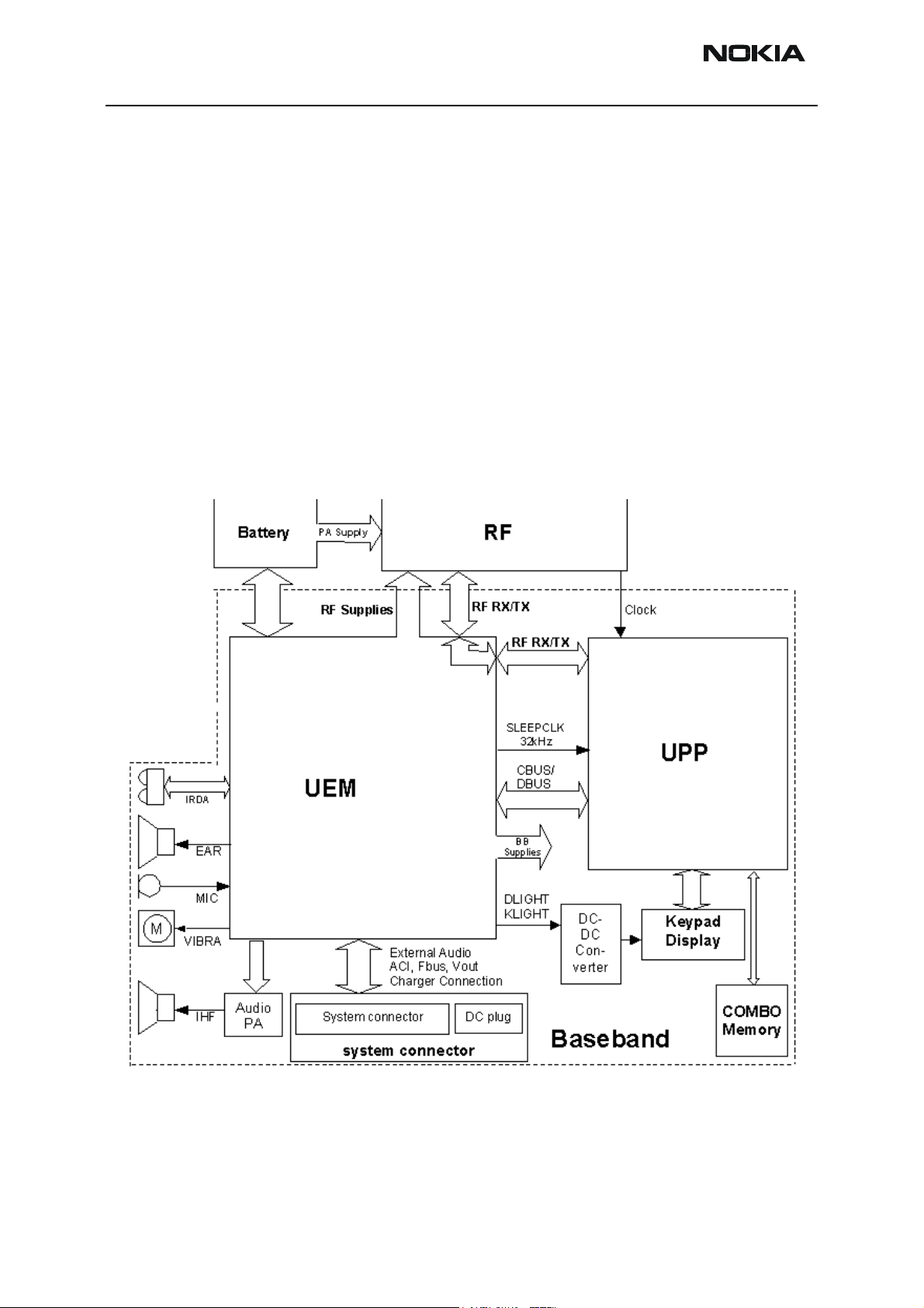
Baseband Top-Level Description
RH-25 is a handportable dual band TDMA and AMPS DCT-4 generation phone for the
smart classic segment.
The RH-25 Baseband consists of the DCT4 common Baseband chipset having some product-specific blocks of its own, such as pop-port system connector (also unofficially
known as "Tomahawk"), IHF, IrDA, and a color display.
The Baseband engine consists basically of two major ASICs:
• Universal Energy Management IC (UEM), including the analog audio circuits, the
charge control, and the voltage regulators.
• Universal Phone Processor (UPP), containing DSP, MCU, and some internal memory.
Baseband Block Diagram
The system block diagram below shows the main BB functional blocks.
Figure 1: Baseband block diagram
Page 4 © 2003 Nokia Corporation Confidential Issue 1 10/2003
Page 5
RH-25
CCS Technical Documentation Troubleshooting - Baseband
Environmental Specifications
Normal and Extreme Voltages
Following voltages are assumed as normal and extreme voltages for the BLD-3 battery
used in RH-25:
• Nominal voltage: 3.6 V
• Lower extreme voltage: 3.1 V
• Higher extreme voltage (fast charging): 4.4 V
Temperature Conditions
Operational temperature range (all specifications met within this range)
-10°C..+55°C
Functional temperature range (Reduced performance) -30°C..+70°C
Storage temperature range: -30°C..+85°C
Humidity
Relative humidity range is 5...95%.
The Baseband module is not protected against water. Condensed or splashed water may
cause interim or permanent phone malfunction.
Submergence of the phone in water will likely cause permanent damage to the phone.
Frequencies in Baseband
There are several clock frequencies at the baseband part. The following table lists all
available frequencies. The asynchronous and diagnostic busses are not included.
Frequency Context UPP UEM Flash Comments
54 MHz Memory clock X X
19.44 MHz RF clock X
13MHz DBUS, RFBusClk X X
Up to 1MHz RFConvClk X X
Table 1: Frequency List
1.08MHz CBUS Clock X X AMPS mode: 1.25MHz
32kHz Sleep Clock X
1.2kHz ACI X X
1.625MHz
up to 6.5MHz
Display IF X Frequency depends on
SW
Issue 1 10/2003 Confidential © 2003 Nokia Corporation Page 5
Page 6

RH-25
Troubleshooting - Baseband CCS Technical Documentation
Infrared Interface (IrDA)
RH-25 supports data connectivity via an infrared link. An IR module is integrated into
the phone, connected to the IR interface of the UPP ASIC.
Energy Management
The energy management of RH-25 is based on BB 4.0 architecture. A semi-fixed battery
(BLD-3) supplies power primarily to UEM ASIC and the RF PA. UEM includes several regulators to supply RF and baseband. It provides the energy management including power
up/down procedure.
Power Supply Modes
The functional behavior of the UEM can be divided into seven different states. Since the
UEM controls the regulated power distribution of the phone, each of these states affects
the general functionality of the phone:
•No supply
• Backup
•Power off
• Reset
•Power on
• Sleep
•Protection
The different states of the UEM are detailed in the sections below.
No Supply
In the NO_SUPPLY mode, the UEM has no supply voltage (VBAT < V
V_BU
tery are either disconnected or both discharged to a low voltage level.
The UEM will recover from NO_SUPPLY into RESET mode if the VBAT voltage level rises
above the V
Backup
In BACK_UP mode the main battery is either disconnected or has a low voltage level
(VBAT < V
and VBACK <
MSTR
). This mode is due to the fact that both the main battery and the backup bat-
COFF-
level by either reconnecting the main battery or charge it to such level.
MSTR+
and VBACK > V_BU
MSTR-
COFF+
).
The regulator VRTC that supplies the real-time clock is disabled in BACK_UP mode.
Instead the unregulated backup battery voltage VBACK supplies the output of the VRTC.
All other regulators are disabled and the phone has no functionality.
The UEM will recover from BACK_UP mode into RESET mode if VBAT rises above V
MSTR+
Power Off
In order for the UEM to be in PWR_OFF mode, it must have supply voltage (VBAT >
V
MSTR+
).
Page 6 © 2003 Nokia Corporation Confidential Issue 1 10/2003
.
Page 7

RH-25
CCS Technical Documentation Troubleshooting - Baseband
The regulator VRTC regulator is enabled and supplying the RTC within the UEM. The UEM
will enter RESET mode after a 20 ms delay whenever one of the below listed conditions is
logically true:
• The power button is activated
• Charger connection is detected
• RTC alarm is detected
The UEM will enter PWR_OFF from all other modes except NO_SUPPLY and BACK_UP if
the internal watchdog elapses.
Reset
When the UEM enters RESET mode from PWR_OFF mode, the watchdog is enabled. If the
VBAT fails to rise above the power-up voltage level V
(3.1 V) before the watchdog
COFF+
elapses, the UEM will enter PWR_OFF mode. Otherwise, after a 200 ms delay, the regulator VFLASH1 will be enabled and after an additional delay of 500 µs, the regulators
VANA, VIO, VCORE, and VR3 will be enabled. All other regulators( i.e., VFLASH2, VSIM,
VR1, VR2, and VR4 - VR7) are software controlled and disabled by default. After an additional delay of 20 ms, the UEM enters PWR_ON mode.
Power On
In PWR_ON, the UEM is fully functional in the sense that all internal circuits are powered up or can be by means of software. The UEM will enter PWR_OFF mode if VBAT
drops below V
enter PWR_OFF mode if either of the watchdogs Operational State Machine (approx. 100
µs), Security (32 sec.), or Power Key (4 sec.) elapses or if any of the regulators trigger the
thermal protection circuitry
Sleep
The UEM can be forced into SLEEP mode by the UPP by setting the input SLEEPX low for
more than 60 µs. This state is entered when the external UPP activity is low (phone in
sleep) and thereby lowering the internal current consumption of the UEM. The regulator
VANA is disabled and VR1 - VR7 are either disabled or in low quiescent mode.
From SLEEP the UEM enters PWR_ON if SLEEPX goes high, PWR_OFF mode if watchdog
elapses or BACK_UP mode if VBAT drops below V
Protection Mode
The UEM has two separate protection limits for over temperature conditions: one for the
charging switch and one for the regulators. The temperature circuitry measures the onchip temperature. In case of charging over temperature, the circuit turns the charging
switch off. In case of over temperature in any of the regulators, the UEM powers off.
for a period of time longer than 5 µs. The UEM will furthermore
COOF-
.
MSTR-
Battery BLD-3
RH-25 uses the BLD-3 Li-ion battery with a capacity of 780mAh. BLD-3 is a case-less
battery; the main advantage of a case-less battery type is the overall size, particularly
the thickness and the number of contact terminals.
Issue 1 10/2003 Confidential © 2003 Nokia Corporation Page 7
Page 8

RH-25
Troubleshooting - Baseband CCS Technical Documentation
BLD-3 has a four-pin connector. BSI resistor value is 75Kohm.
Power Distribution
Under normal conditions, the battery powers the baseband module. Individual regulators
located within the UEM regulate the battery voltage VBAT. These regulators supply the
different parts of the phone. Eight regulators are dedicated to the RF module of the
phone, and six to the baseband module.
The regulator VCORE is likewise adjustable and controlled by registers written by the
MCU. VCORE supplies the core of the UPP and can be adjusted on the fly by the MCU if
DSP capacity is inadequate. Higher VCORE supply (1.8 V) results in faster core operations
in the UPP.
Regulators VANA, VFLASH1, and VIO are solely controlled by the UEM and cannot be
enabled or disabled by the MCU. Furthermore, VFLASH1 and VIO are both ON, though in
low quiescent mode when phone is in sleep mode. An output current of 500 µA can be
drawn from the regulators. VIO supplies the UPP, FLASH and LCD, VFLASH1 supplies LCD
and the IrDA module. VANA is supplying analog parts internally in the UEM as well as the
baseband audio circuitry and pull-up resistors on the input of the UEM slow AD converters.
System connector provides a voltage to supply accessories. The white LED's need a higher
voltage supply as the battery can provide in bad condition. Separate external regulators
supply both consumers.
The regulators VR1A, VR1B, VR2 - VR7 and IPA1 - IPA4 are controlled by the DSP via
the DBus. VR4 - VR7 are controlled by the UEM as well and are disabled in sleep regardless of DSP writings.
VBAT/VBATTRF is furthermore distributed, unregulated, to the RF power amplifier, audio
power amplifier and external baseband regulators.
The CHACON module in the UEM controls the charging of the main battery. Furthermore
it contains a 3.2 Vdc regulator for charging of the backup battery and a 1.8 Vdc regulator
supplying the internal real time clock.
Page 8 © 2003 Nokia Corporation Confidential Issue 1 10/2003
Page 9
RH-25
V
CCS Technical Documentation Troubleshooting - Baseband
Baseband
UEM
RF Regulators
VR1A
VR1B
VR2-7
6
SIM
VSIM
Battery
BAT
LED
regulator
ACC
regulator
PA Supply
VCORE
Baseband
Regulators
RTC
CHACON
VOUT
Tomahawk System Connector
VANA
VIO
VFLASH1
VFLASH2
Figure 2: Baseband power distribution
IHF PA
UPP
FLASH
LCD
Backup
battery
LED
Keyboard/display
IRDA
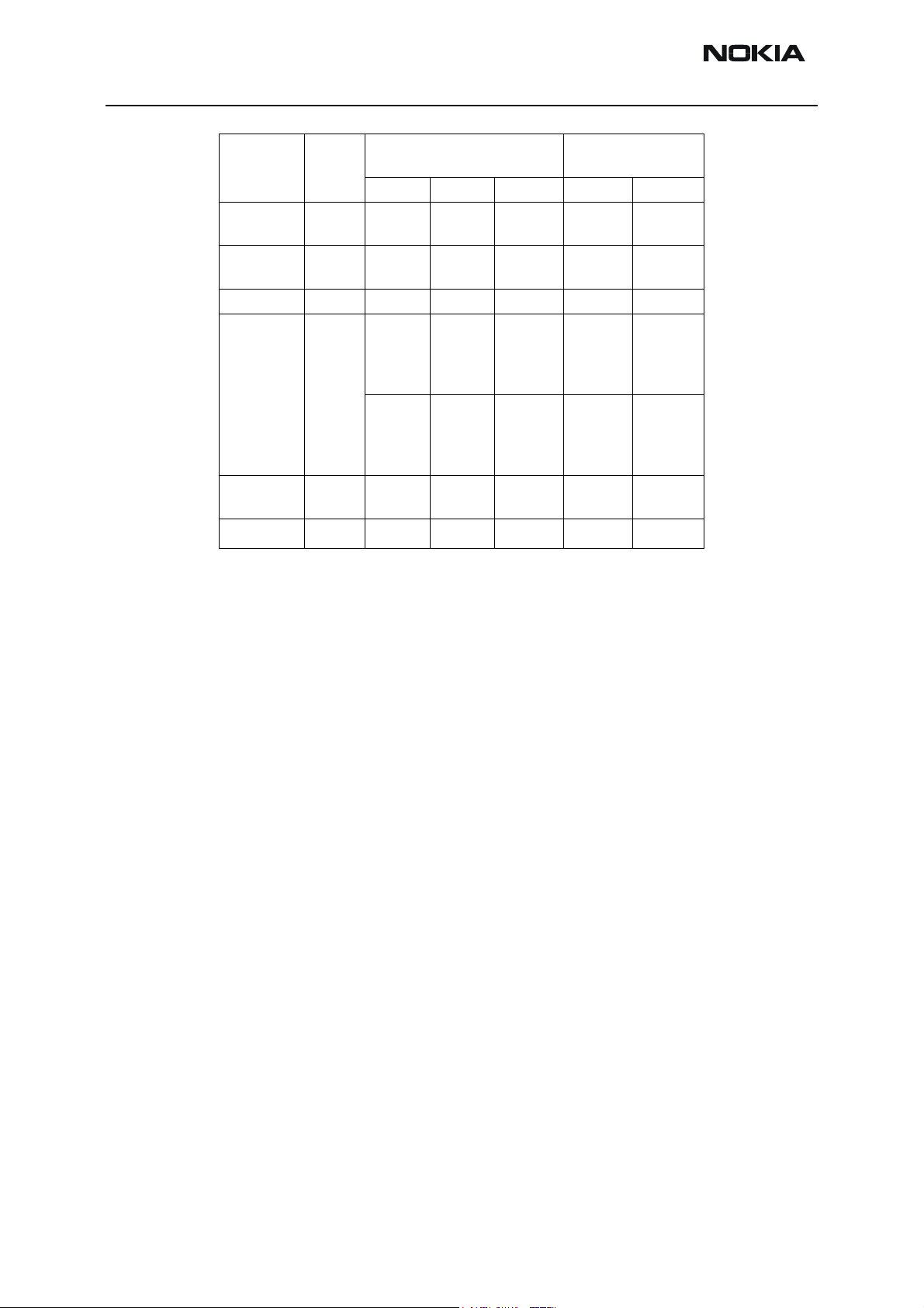
DC Characteristics
The following table reflects the specifications of voltage and current regulators within
the UEM:
Regulator Target
VR1A RF 4.6 4.75 4.9 0 10
4
VR2
VR3 RF 2.70 2.78 2.86 0.1 20
VR4 RF 2.70 2.78 2.86 0.1 50
VR5, VR6
VR7 RF 2.70 2.78 2.86 0.1 45
VrefRF01 RF 1.334 1.35 1.366 - 0.1
Table 2: UEM regulator outputs
Output Voltage (V) Output Current
(mA)
Min Typ Max Min Max
RF 2.70 2.78 2.86 0.1 100
0.1
1
RF 2.70 2.78 2.86 0.1 50
0.1
Issue 1 10/2003 Confidential © 2003 Nokia Corporation Page 9
Page 10
RH-25
Troubleshooting - Baseband CCS Technical Documentation
Output Voltage (V) Output Current
Regulator Target
Min Typ Max Min Max
1
VIO
2
VSIM
VANA BB 2.70 2.78 2.86 0.005 80
2
VCORE
VFLASH1 BB 2.70 2.78 2.86 0.005
VFLASH2
3
BB 1.72 1.8 1.88 0.005
BB 1.745
2.91
BB 1.000
1.235
1.425
1.710
0.974
1.215
1.410
1.692
BB 2.70 2.78 2.86 0.005 40
1.8
3.0
1.053
1.3
1.5
1.8
1.053
1.3
1.5
1.8
1.855
3.09
1.106
1.365
1.575
1.890
1.132
1.365
1.575
1.890
0.005
0.005
0.005
0.005
0.005
0.005
0.005
70
85
100
120
0.005
(mA)
150
0.500
25
0.500
70
85
100
120
200
200
200
200
70
1.5
1 The second current value indicates the maximum possible output current of the
regulator when in low quiescent mode.
2 The output voltages are split into two different current categories. The upper part
is the lower range of output current, and the lower part is the higher range of
output current.
3 Condition in sleep-mode depends on MCU writings to UEM regulator register
solely.
4 Condition in sleep-mode depends on DSP writings to UEM register.
When the accessory regulator, N100, is active, it will turn Vout ON (2.8V) and provide
70mA current.
Audio Circuitry
This section describes the audio-HW inside the Baseband. (External audio components
and acoustics are not considered with the details in this section.)
The main topology comes from other phones using BB4.0 engine, where the audio-HW is
mostly integrated into the UEM-ASIC. The biggest difference is that RH-25 has integrated hands-free (IHF).
Page 10 © 2003 Nokia Corporation Confidential Issue 1 10/2003
Page 11
RH-25
CCS Technical Documentation Troubleshooting - Baseband
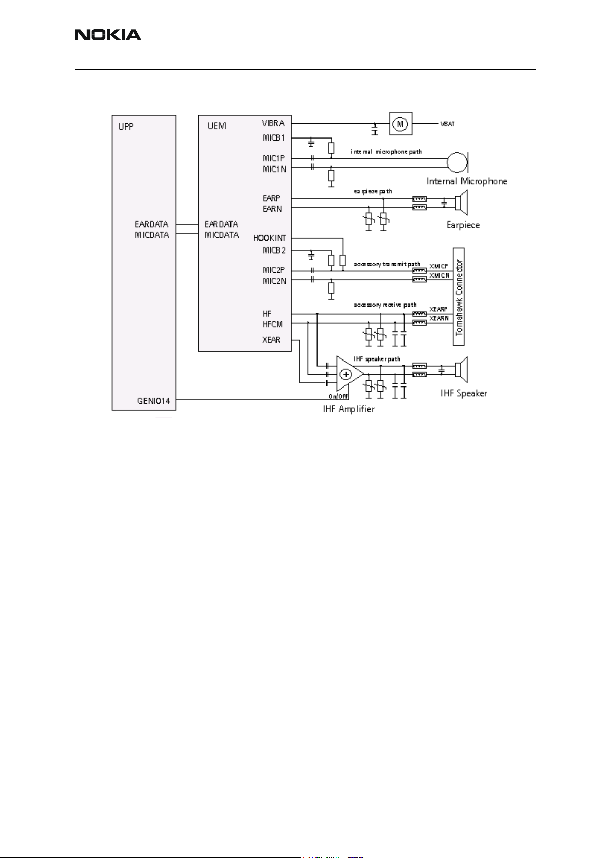
Audio Block Diagram
Earpiece
RH-25 uses an earpiece, which is also referred to as a PICO speaker. This is a 32 ohm
speaker with the diameter of 8 mm.
Earpiece is fed by the differential signals EARP and EARN from UEM. The signals run
quite directly from UEM to the earpiece, only some passive ands EMC protection components are needed
The external earpiece signals are fed by the HF and HFCM pins.
The level (swing) of earpiece-signals can be adjusted by register values inside UEM. These
signals have a common voltage level of 1.35 V (0.8 V for HF) at UEM pins.
Microphones
An EMC-improved type of microphone is used as internal microphone in RH-25, diameter
of which is 2.2mm.
Internal microphone circuitry is driven single-ended. Microphone needs bias voltage,
which is provided by UEM and is fed through a resistor to the microphone. A resistor is
also needed to the other side of the microphone, (i.e., between microphone and GND), in
order to provide the differential signals to UEM. Audio signals are AC-coupled from the
microphone.
Figure 3: Audio block diagram
Issue 1 10/2003 Confidential © 2003 Nokia Corporation Page 11
Page 12

RH-25
Troubleshooting - Baseband CCS Technical Documentation
For the external microphone a differential input is used.
MIC1N and MIC1P (audio signals) and MICB1 (bias voltage) are used for the internal
microphone. MIC2N and MIC2P and MICB2 are used for external microphone.
Integrated Hands-free (IHF)
The speaker used for IHF is a 16 mm diameter speaker with 8 Ohm impedance, also
known as a MALT speaker.
IHF circuitry uses differential outputs from UEM.
Depending on the audio mode, the IHF amplifier is driven either from UEM HF / HFCM or
XEAR audio outputs. The IHF audio power amplifier (APA) LM4855 has a bridge-tied-load
(BTL) output in order to get the maximum use of supply voltage. The supply voltage for
driving circuitry of speaker is VBAT, thus the swing across the speaker is (VBAT.
The shutdown of the IHF PA is controlled by UPP using GENIO14.
Audio Accessory Receive Path
In RH-25, the accessory receive path is directly driven from UEM HF / HFCM differential
audio outputs, the output signal complies with the Pop-port accessory interface.
For EMC protection, ferrites are connected in series to the earpiece; for ESD protection,
varistors are used.
Audio Control Signals
The HEADINT signal is needed for recognizing the external device (e.g., headset) connected to the system. The recognition is based on the ACI-pin on the system connector,
which is shorted to ground inside the external device.
The button of the external device generates HOOKINT. This is used to answer or to end a
phone call.
Acoustics
Earpiece Acoustic
RH-25 uses the PICO 8mm earpiece.
This earpiece is mounted into the UI-shield assembly, the sealing of the front volume is
achieved using a foam gasket mounted on the front of the speaker. The UI shield is sealed
using a rubber sealing between UI shield and A-cover to create an acoustic path.
IHF Speaker Acoustics
The MALT speaker is used in RH-25 for integrated hands-free and ringing tone applications.
The IHF speaker is mounted to the IHF enclosure on a foam sealing ring. The IHF enclo-
Page 12 © 2003 Nokia Corporation Confidential Issue 1 10/2003
Page 13

RH-25
CCS Technical Documentation Troubleshooting - Baseband
sure provides the needed back volume for the speaker. The IHF enclosure is closed with
the IHF lid, which is carrying the IHF pins to contact the IHF speaker.
The sealing of the effective acoustic volumes is achieved using ultrasonic welding to
bond the IHF lid and the IHF enclosure permanently.
To provide long-term reliability, additionally the IHF lid is heat stacked to the IHF enclosure. There is a dust membrane mounted inside the acoustic chamber that provides dust
and drop protection.
Due to ultrasonic welding of the IHF enclosure, it cannot be disassembled and, in case of
failure, the C-cover assembly should be replaced as one complete assembly.
Microphone Acoustics
A standard microphone module is used. This module is embedded into a rubber boot and
connected to the RH-25 system module by spring contacts.
The microphone is placed close to the system connector. The sound port of the microphone is located towards the bottom of the phone.
Vibra Motor
A vibrating alerting device is used to generate a vibration signal for an incoming call.
This vibra is located in the bottom section of the phone.
The vibrator is driven by the UEM output VIBRA, and controlled with a PWM signal. The
supply of the vibra is taken from the battery voltage of the phone.
Audio Modes
The following audio configurations can create the audio modes:
• Handportable
• Integrated hands-free
• Headset
• Loop set
• External hands-free
The following audio sources have to be routed according to the active audio mode:
• Speech
• Ringing tones / SMS tones
• Keypad tones
• Error tones / Warning tones
• Game tones
Handportable Mode
In handportable mode, earpiece path and internal microphone path are in use. The audio
sources are routed according to the following table:
Issue 1 10/2003 Confidential © 2003 Nokia Corporation Page 13
Page 14

RH-25
Troubleshooting - Baseband CCS Technical Documentation
Table 3: Handportable mode audio routing
Audio Source Earpiece
Speech X X
Ringing tones, SMS tones X
Keypad tones X
Warning/Error tone X
Game tones X
Internal
Microphone
Integrated Hands-free Audio Mode
In integrated hands-free mode, IHF path and internal microphone path are used. The
audio sources are routed according to the following table:
Table 4: IHF mode audio routing
Audio Source Earpiece
Speech X X
Ringing tones, SMS tones X
Internal
Microphone
IHF
speaker
IHF speaker
Accessory
receive path
Accessory
receive path
Accessory
transmit path
Accessory
transmit path
Keypad tones X
Warning/Error tones X
Game tones X
Headset Audio Mode
In headset mode, accessory receive path and accessory transmit path are used. RH-25
supports the following headsets:
HDB-4: HS-10, HS-5, and HS-2R headsets
The audio sources are routed according to the following table:
Table 5: Headset audio mode routings
Audio Source Earpiece
Speech X X X
Ringing tones, SMS tones X X
Keypad tones X
Internal
Microphone
IHF speaker
Accessory
receive path
Accessory
transmit path
Warning/Error tones X
Game tones X
Page 14 © 2003 Nokia Corporation Confidential Issue 1 10/2003
Page 15

RH-25
CCS Technical Documentation Troubleshooting - Baseband
Loop set Audio Mode
In loop set mode, accessory receive path and accessory transmit path are used. RH-25
supports the loop set LPS-4.:
Table 6: Loop set mode audio routing
Audio Source Earpiece
Speech X X
Ringing tones, SMS tones X X
Keypad tones X
Warning/Error tones X
Game tones X
Internal
Microphone
IHF speaker
Accessory
receive path
External Hands-free Audio Mode
In external hands-free mode, accessory receive path and accessory transmit path are
used. RH-25 supports external hands-free accessories:
BHF-1: Basic car hands-free kit
Table 7: External hands-free mode audio routing
Audio Source Earpiece
Speech X X
Internal
Microphone
IHF speaker
Accessory
receive path
Accessory
transmit path
Accessory
transmit path
Ringing tones, SMS tones X
Keypad tones X
Warning/Error tones X
Game tones X
System Connector Interface
System Connector
The system connector in RH-25 is called Pop-Port System Connector (unofficial name:
"Tomahawk"). It is a galvanic interface between phone and accessories.
Compared with previous system connector versions, four new functions are introduced
with the Pop-port system connector interface:
• Accessory Control Interface (ACI)
•Power Out
• Stereo audio output
• Universal Serial Bus (USB).
USB functionality and stereo audio output of the Pop-port are not supported in RH-25.
Issue 1 10/2003 Confidential © 2003 Nokia Corporation Page 15
Page 16

RH-25
N
Troubleshooting - Baseband CCS Technical Documentation
Pop-port system connector is mechanically and electrically not backward-compatible
with any earlier Nokia accessory interfaces, except the charger connector.
ACI
Vout
Charge
Charge GND
Shielding GND
Fbus TX
Fbus RX
XMIC N
XMIC P
DATA GND
HSEAR_L_P
HSEAR_L_N
HSEAR_R_N
Figure 4: Tomahawk (Pop-port) system connector
Table 8: Tomahawk system connector interface description
Pin # Signal Notes
1 VCHAR Charger input line
2 GND Charge ground
3 ACI Insertion and removal detection/ Serial data bi-
directional 1 kbit/s
4 Vout Accessory power supply
5 Not used in RH-25
6 FBUS_RX Serial data from accessory to phone / 115 kbit/s
7 FBUS_TX Serial data from phone to accessory / 115 kbit/s
HSEAR_R_P
Shielding GND
8GND Data ground
9 XMIC N Negative audio in signal
10 XMIC P Positive audio in signal
11 HSEAR_L_N Negative left channel audio out signal
12 HSEAR_L_P Positive left channel audio out signal
13 HSEAR_R_N Negative right channel audio out signal
14 HSEAR_R_P Positive right channel audio out signal
Accessory Control Interface (ACI)
ACI is a point-to-point, master-slave, and bi-directional serial bus. It has three features:
• The insertion and removal detection of an accessory device
• Acting as a data bus, intended mainly for control purposes
• The identification and authentication of accessory type which is connected
The accessories are detected by the HeadInt signal when the plug is inserted.
Max bandwidth from the phone
Max bandwidth from the phone
Page 16 © 2003 Nokia Corporation Confidential Issue 1 10/2003
Page 17

RH-25
d
+
t
K
)
t
g
r
y
K
CCS Technical Documentation Troubleshooting - Baseband
Normally when no plug is present, the pull-up resistor 100k pulls up the HeadInt signal
to VFLASH1. If the accessory is inserted, the external insertion and removal resistor
works as voltage divider and decreases the voltage level below the threshold Vhead.
The comparator output will be changed to high state causing an interrupt.
If the plug is removed, the voltage level of HeadInt increases again to VFLASH1. This
voltage level is higher than the threshold of the comparator and therefore its output will
be changed to low. This change leads to an interrupt. These HeadInt interrupts initiate
the accessory detection or removal sequence.
If no accessory is inserted / connected, the only active part on the Pop-port interface is
the ACI line.
ACI Accessor
Insertion &
Removal
detection
56
Data
GND
Accessory
Detect
VFLASH1
VFLASH1
4k7
UEM
HookInt
-
Vhea
MBUS
HeadIn
VFLASH1
47R 47R
ProdTP7
PHONE
100
ACI
ChargeGND
VBAT
Voltage
en
ulato
Re
UPP
GenIo(0
Figure 5: Principle schematics of ACI accessory and engine
Signal flow on ACI line - ACI-ASIC accessory inserted
1. Accessory is connected (insertion and removal resistor connect to ACI line)
1a) Phone gets HeadInt interrupt after 20ms check that ACI line is still low (<Vhead min)
2. Connect MBUS with HeadInt line (MBUS switch)
2a) If the phone detects a HeadInt interrupt from low to high transition in 20ms time-
frame, then an advanced accessory is connected
3. ACI chip reset (3000- 4000us)
4. Power up delay (50-400us)
5. Start bit (50us)
Vou
ACI
ASIC
VCC
6. Learning sequence (567-1700us)
7. ACI communication
8. MBUS is disconnected from HeadInt line (MBUS switch). After every communication.
9. Accessory is removed (no insertion and removal resistor on ACI line) --> phone gets
Issue 1 10/2003 Confidential © 2003 Nokia Corporation Page 17
Page 18

RH-25
Troubleshooting - Baseband CCS Technical Documentation
HeadInt interrupt from ACI line low to high transition.
9a) If no HeadInt interrupt comes in the next 100ms, the accessory is really removed and
the phone goes in the state "no accessory".
Table 9: Voltage levels
Signal Min Typ Max Unit Notes
V
FLASH1
V
head
Specified val-
2.7 2.78 2.86 V
1.75 1.9 2.05 V
Min Typ Max Unit
ues for levels
V
act_detect
0.83 1.13 V Voltage level if MBUS not connected to HeadInt
(MBUS switch open), but ACI accessory is
inserted.
V
V
high
low
2.45 2.71 V Voltage level after MBUS connected to HeadInt
<0.22*VDD V
Signal flow on ACI line - Non ACI-ASIC accessory inserted
V
headInt
V
FLASH1
V
head_min
1
20ms
2
1
a
V
low
3
Mono Headset is
recognized.
3
a
4
a
4
FBUS
Figure 6: Signal flow on ACI Line
1. Accessory is connected (insertion and removal resistor connect to ACI line)
1a) Phone gets HeadInt interrupt after 20ms check that ACI line is still low (<Vhead min)
2. Connect MBUS with HeadInt line (MBUS switch)
3. The 20 ms timer elapsed and no transition has been on HeadInt line
3a) Disconnect MBUS from HeadInt line
4. Accessory is removed. Phone gets HeadInt interrupt from ACI line low to high transition.
4a) If no HeadInt interrupt comes in the next 100ms, the accessory is really removed.
FBUS is an asynchronous data bus with separate TX and RX signals. Default bit rate of
the bus is 115.2 Kbit/s.
FBUS is used as additional communication channel from phone to accessory and vice
versa. There are two types of accessories which it uses:
Page 18 © 2003 Nokia Corporation Confidential Issue 1 10/2003
Page 19

RH-25
CCS Technical Documentation Troubleshooting - Baseband
1. Nokia Serial Bus Accessory, AT mode
2. Fbus Phonet mode accessory
From HW-point of view, this does not make any difference.
Table 10: FBUS interface
Signal Parameter Min Typ Max Unit
FBUS_RX V
FBUX_TX V
IH
V
IL
OH
V
OL
VOUT (Accessory Voltage Regulator)
DCT4 chip set does not provide and power supply for accessories. To enable this, an
external LDO regulator is needed. This regulator is called Accessory Regulator.
The regulator input is connected directly to battery voltage (VBAT) and the output to
VOUT pin at system connector. The regulator is controlled by the GENIO(0) line of UPP.
With this signal, the regulator can be switched on and off.
The regulator can be supply up to150 mA. (Note: this exceeds the Pop-port minimum
requirement.)
VBAT
UPP
GenIO(0)
1.95 2.78 3.0 Vout
0 0.2 0.83
1.95 2.78 2.83
0 0.2 0.83
Tomahawk
bottom connector
Voltage
regulator
En
LP3985
VOUT
0.9R
DC resistance of ferrite
+ impedance of line and connector
Figure 7: Accessory power supply diagram
Table 11: Accessories power supply
Signal Min Nom Max Unit Note
Vout 2.63
2.56
GenIO(0) 1.4 1.88
2.80 2.88 V I = 70mA
Imax = 150mA
0.6 V High (ON)
0.6
Low (OFF)
The pull-down resistor on the enable input of the regulator is needed because in the
switch-off mode of the phone, the output level of the Genio(0) is not defined. Without
this resistor the output of the regulator can be floating.
Issue 1 10/2003 Confidential © 2003 Nokia Corporation Page 19
Page 20

RH-25
Troubleshooting - Baseband CCS Technical Documentation
RH-25 supports fully differential external audio signals. A headset can be connected to
the Pop-port system connector. However, only Mono audio is supplied to accessories.
HookInt
This signal is used to detect whether a button in accessory is pressed or not. The hook
signal is generated by creating a short circuit (20 ohm) between the headset microphone
signals (XMICP and XMICN). In this case, an LP-filter is needed on the HookInt input to
filter the audio signal.
If no accessory is present, the HookInt signal is pulled up by the UEM resistor.
If an accessory is inserted and the microphone path is biased, the HookInt signal
decreases to 1.9V due to the microphone bias current flowing through the resistor. When
the button is pressed, the microphone signals are connected together, and the HookInt
input will get half of micbias dc value 1.1V. This change in DC level will cause the HookInt comparator output to change state, in this case from 0 to 1.
HookInt comparator reference is selected level is 1.35 V.
Normally micbias and hookint are enabled only when audios are routed to headset.
In order to recognize the Hook signal (button in headset or SyncButton in deskstand),
when the phone is in the sleep mode, it must be done by polling. That means the micbias
and the hookInt signal must be enabled in regular time intervals.
Charging
RH-25 can be charged via a DC-plug or charging pins on the system connector. It supports only 2-wire charging.
Table 12: Voltage levels Hook Int
Signal Min Nom Max Unit
VFLASH1 2.7 2.78 2.86 V
MICB2 2.0 2.1 2.25
600
Vhook1 1.25 1.35 1.45 V
V
uA
DC-Plug
RH-25 uses a 3.5mm DC-plug. It is possible to use a 3-wire charger, but the PWM inside
these chargers is not supported.
VCHAR Pins of System Connector
The VCHAR and ChargeGND pin are directly connected to the normal charger lines of the
Page 20 © 2003 Nokia Corporation Confidential Issue 1 10/2003
Page 21

RH-25
CCS Technical Documentation Troubleshooting - Baseband
DC-plug.
Table 13: Charger input voltage levels
Signal Min Nom Max Unit Notes
Input voltage range
(fast charger)
Input voltage range
(standard charger)
5.5 8.4 9.3 VRMS 1 = 850mA
11 .1
7.9
-0.3 20 V Absolute maximum VCHAR voltage
16 Vpeak
VRMS
Issue 1 10/2003 Confidential © 2003 Nokia Corporation Page 21
Page 22

RH-25
Troubleshooting - Baseband CCS Technical Documentation
Voltages and Currents
Table 14: System connector interface signals
Pin # Signal Parameter Min Typ Max Unit Notes
1VCHAR 0 9
0.85
2 GND Charge ground
3 ACI Logic “0”
Logic “1”
4 Vout Output voltage
Current
5 Not used in RH-25
6 FBUX_RX Logic “0”
Logic “1”
7 FBUS_TX Logic “0”
Logic “1”
8 GND Data ground
9 XMIC N Differential
voltage swing
DC level
0
1.7
2.56 2.8
0
2.0
0
1.89
0.2
2.78
70
0.2
2.78
0.2
2.78
1Vpp
0.7
2.86
2.88
150
0.86
3.0
0.81
2.83
VDC
ADC
V Insertion and removal
detection/ Serial data
bi-directional 1 kbit/s
VDC
mA
V Serial data from
V Serial data from
VDC
70mA is specified as
the max current in the
Pop-port specification
accessory to phone /
115 kbit/s
phone to accessory /
115 kbit/s
Negative audio in signal
10 XMIC P Differential
voltage swing
DC level 2.05
11 HSEAR_L_N Differential
voltage swing
12 HSEAR_L_P Differential
voltage swing
13 HSEAR_R_N Differential
voltage swing
14 HSEAR_R_P Differential
voltage swing
1
2.1 2.25
400
1 Vpp Left channel negative
1 Vpp Left channel positive
1 Vpp Right channel nega-
1 Vpp Right channel positive
Vpp
VDC
uA
Positive audio in signal
audio out signal
audio out signal
tive audio out signal
audio out signal
Page 22 © 2003 Nokia Corporation Confidential Issue 1 10/2003
Page 23

RH-25
CCS Technical Documentation Troubleshooting - Baseband
Main Troubleshooting Diagram
Top
Phone totally dead
NO
Flash programming
doesn't work
NO
Phone doesn't start
up or phone is
jammed
NO
Charging doesn't
work
YES
YES
YES
YES
Phone
dead
Flash
faults
Phone
is
jammed
Charger
faults
NO
IrDa doesn't work IrDa fault
NO
YES
Top page 2
Issue 1 10/2003 Confidential © 2003 Nokia Corporation Page 23
Page 24

RH-25
Troubleshooting - Baseband CCS Technical Documentation
Top 2
Audio faults
NO
Display or LEDs not
working
NO
Keypad doesn't work
NO
Accessory doesn't
work
NO
YES
YES
YES
YES
Audio
faults
Display
faults
Keypad
faults
Access
ory
faults
Illumination doesn't
work
NO
YES
END
Illumina
tion
faults
Page 24 © 2003 Nokia Corporation Confidential Issue 1 10/2003
Page 25

RH-25
CCS Technical Documentation Troubleshooting - Baseband
Phone is Dead
Phone
is dead
Check X100
Is phone current
0 mA?
YES NO
(contacts,
solderings). Is it
OK?
YES
Change X100
NO
Phone current is
<50 mA
NO
Phone current is
~54 mA
YES
Is phone in Local
Mode?
Check power key Change if defective
YES
NO
Check all VBAT lines
Is flash
YES YES
programming
working OK?
NO
NO
Check X100, R203,
NO YES
R204, C217, and
C220. Replace if
defective.
Phone
is
jammed
Flash
faults
Change UEM
YES
End
NO
Change
defective part
Issue 1 10/2003 Confidential © 2003 Nokia Corporation Page 25
Page 26

RH-25
Troubleshooting - Baseband CCS Technical Documentation
Flash Programming Fault
Flash
faults
Is the FBUS TX line
HIGH after startup?
YES
Is FBUSTX line set
to LOW after it has
been HIGH?
YES
Wrong manufacturer
ID and device ID
Measure BSI pulse
NO NO
during Flash
programming. Is it
OK?
YES
Measure FBUSTX
line during Flash
operation (J491). Is it
NO
~1.8V?
NO
YES
YES
Check X100, R203,
R204, C217, and
C220. Replace if
defective.
Check R104. If OK,
change UEM
Change UPP
Change Flash
NO
Is phone totally
dead?
NO
Phone doesn't start
up or is jammed
NO
YES
YES
Phone
is dead
Phone
is
jammed
End
(retest)
Page 26 © 2003 Nokia Corporation Confidential Issue 1 10/2003
Page 27

RH-25
CCS Technical Documentation Troubleshooting - Baseband
Flash Programming Does Not Work
Flash programming procedure
1 The phone communicates with the prommer via the production test pattern,
using the following signals:
• FBUSTX (serial data to phone)
• FBUSRX (serial data from phone)
• MBUS (serial clock for FBUSRX)
• VPP (external flashing voltage for speed up flashing)
• The BSI line also is used when initializing flashing (battery connector)
2 When the phone is powered (VBAT>3V), the MBUS and FBUSTX lines are pulled
up internally by the phone.
3 The prommer sends a command to the UEM, using FBUSRX, to enter the Flash
mode. During the sending of this command, the prommer keeps the BSI line high
and MBUS is used as a serial clock.
4 When the Flash mode command is acknowledged, UEM enters the Flash mode
and releases reset (PURX) to MCU.
5 After reset is released, UPP checks if there is a request for the Bootstrap code
that resides in the UPP ROM.
6 The request for Bootstrap is the MBUS pulled down by the prommer (if the boot-
strap is not requested, the bootstrap code jumps to FLASH SW).
7 If the Bootstrap code is requested, UPP enters the Flash mode and sets FBusTX to
‘0’ as an acknowledgement to the prommer. This is an indication that UPP can
run, at least, the fixed Bootstrap code — although it is not able to run the FLASH
code. UPP then sends an UPP ID to the prommer via the FBUSTX line.
8 After the prommer has received the UPP ID, it sends a corresponding Secondary
Boot Code to the phone via FBUSRX. The Secondary Boot Code, when run in UPP,
requests UPP to send information to the prommer about the flash type and other
HW-related parameters about the device to be flashed.
9 The prommer then sends the Algorithm Code corresponding to the HW parame-
ters, and this algorithm, when run in UPP, takes over handling the MCUSW transfer to Flash.
10 To speed up flashing, 12 volts can be supplied to Vpp (by the prommer).
Issue 1 10/2003 Confidential © 2003 Nokia Corporation Page 27
Page 28

RH-25
Troubleshooting - Baseband CCS Technical Documentation
11 The Flash program includes a package of MCU and DSP software and all default
parameters for the phone. The tuning values will be added/rewritten during the
Flash/Alignment phase.
Flash programming error codes
The various error codes can be seen from the FPS-8 Flash menu in Phoenix.
The underlined text in the following table indicates that the item under consideration is
being used for the first time in the flashing sequence.
Table 15: Flash programming error codes
Error Description Not working properly
C101 “The Phone does not set FbusTX line
high after the startup.”
C102 “The Phone does not set FbusTx line low
after the line has been high. The Prommer generates this error also when the
Phone is not connected to the Prommer.”
C103 “Boot serial line fail.” Mbus from Prommer->UEM->UPP(MbusRx)(SA1)
C104 “MCU ID message sending failed in the
Phone.”
C105 “The Phone has not received Secondary
boot codes length bytes correctly.”
C106 “The Phone has not received Secondary
code bytes correctly.”
Vflash 1
VBatt
BSI and FbusRX from prommer to UEM
FbusTX from UPP->UEM->Prommer(SA0)
PURX(also to Safari)
VR3
Rfclock(VCTCXO->Safari->UPP
Mbus from Prommer->UEM->UPP(MbusRx)(SA0)
FbusTx from UPP->UEM->Prommer(SA1)
BSI and FbusRX from prommer to UEM
FbusRX from Prommer->UEM->UPP
FbusTx from UPP->UEM->Prommer
FbusTx from UPP->UEM->Prommer
Mbus from Prommer ->UEM->UPP(MbusRx)
FbusRx from Prommer->UEM->UPP
FbusTx from UPP->UEM->Prommer
Mbus from Prommer->UEM->UPP(MbusRx)
FbusRx from Prommer->UEM->UPP
FbusTx from UPP->UEM->Prommer
C107 “The Phone MCU cannot start Secondary
code correctly.”
C586 “The erasing status response from the
Phone informs about fail.”
C686 “The programming status response from
the Phone informs about fail.”
Cx81 “The Prommer has detected a checksum
error in the message, which it has
received from the Phone.”
UPP
Flash
Flash
FbuxTx from UPP->UEM->Prommer
Page 28 © 2003 Nokia Corporation Confidential Issue 1 10/2003
Page 29

RH-25
CCS Technical Documentation Troubleshooting - Baseband
Table 15: Flash programming error codes
Error Description Not working properly
Cx82 “The PRommer has detected a wrong ID
byte in the message, which it has
received from the Phone.”
A204
Cx83
Cx84
Cx85
Cx87 “Wrong MCU ID.” RFClock
Startup for
flashing
“The flash manufacturer and device IDs
in the existing Algorithm files do not
match with the IDs received from the
target phone.”
“The Prommer has not received Phone
acknowledge to the message.”
“The Phone has generated NAK signal
during data block transfer.”
“Data block handling timeout.”
Required startup for flashing Vflash1
FbuxTx from UPP->UEM->Prommer
Flash
UPP
VIO/VANA?
Signals between UPP-Flash
Mbus from Prommer->UEM->UPP(MbusRx)
FbusRx from Prommer->UEM->UPP
FbusTx from UPP->UEM->Prommer
UPP(Vcore)
VBatt
Issue 1 10/2003 Confidential © 2003 Nokia Corporation Page 29
Page 30

RH-25
Troubleshooting - Baseband CCS Technical Documentation
Phone is Jammed
Phone is
jammed
Measure VIO,
VCORE, VFlash1,
VANA, and VR3
voltages. Are they
OK?
Measure 32kHz
Sleep Clk from test
point J404. Is it OK?
YES
Measure 19.44MHz
RF Clk from C420. Is
it OK?
YES
Check VBATT1-6,
NO NO
VIO, VCORE,
VFlash1, VANA , VR3
lines. Are they OK?
YESYES
NO
Measure Sleep Clk
from B200. Is it OK?
YES
NO
Measure 19.44MHz
NO NO
RFClk from G790. Is
it OK?
YES
Check BSI/BTEMP
lines and VBATT
lines
Check BSI/BTEMP
lines. If OK, UEM
regulators are not
working. Change
UEM.
Check B200, C203,
and C204
Change UEM
Check G790. If not
OK, change.
Check R420. If OK,
change N801.
Measure PURX
signal from test
point J402. Is it
NO
Change UEM
~1.8V?
YES
Phone is
jammed,
page 2
Page 30 © 2003 Nokia Corporation Confidential Issue 1 10/2003
Page 31

RH-25
CCS Technical Documentation Troubleshooting - Baseband
Phone is
jammed,
page 2
Measure 13MHz Clk
Phone shutdown
after 30 seconds
NO
Measure 1.08MHz
Clk signal from test
point J406. Is it OK?
YES NO
DBUSCLK signal
from test point J413.
Is it OK?
NO
Change UPP
YES
Read phone info. Is
it OK?
YES
END
Measure FBUSRX
NO NO
signal during phone
info read from test
point J412. Is it OK?
YES
Measure FBUSTX
signal during phone
info read from test
NO
point J411. Is it OK?
YES
Change UEM
Change UPP
Change UEM
Issue 1 10/2003 Confidential © 2003 Nokia Corporation Page 31
Page 32

RH-25
Troubleshooting - Baseband CCS Technical Documentation
Charger Faults
Charger
faults
Battery bars are
working (scroll)
NO
Measure voltage
over V100 (TVS). Is
it > 3.0 V?
YES
Read BTEMP
value. Compare it
to ambient
temperature. Is it
~25C?
YES
Measure charger
current through
F100. Is it
~350...390mA (with
ACP-7)?
Check X102,
NO
F100, L100,
V100, C124, C127
and line.
Check X100,
C137, C138,
NO
R203, R205,
C217 and line.
Are they OK?
Check R200. Is
NO
it OK?
YES
NO
Change defective
part (if any),
recalibrate charge
current/voltage.
Recalibrate
BTEMP with
YES
Phoenix SW.
defective part,
recalibrate and
YES
Change UEM
Retest
Retest.
Retest
Change
retest
YES
NO
END
Change
defective part,
recalibrate
charge current/
voltage. Retest.
Page 32 © 2003 Nokia Corporation Confidential Issue 1 10/2003
Page 33

RH-25
CCS Technical Documentation Troubleshooting - Baseband
Audio Faults
Audio
faults
Is the earpiece
working?
YES
NO YES
Change earpiece. Is
it working now?
NO
Set phone in LOCAL mode.
Use Phoenix A udio test. Set
EXT IN, HP OUT, LOOP ON
Measure DC offset voltage
from earpiece pads. Is it
NO
~1.38V?
YES
Measure MIC2B
voltage from XMICP
NO
(L102). Is it ~2.2V?
YES
Connect EXT audio signal
(1kHz sine, 200mVpp) in
XMICP and GND in XMICN.
Retest earpiece
Check L131, C107,
C108 and lines. If OK,
change UEM.
Check C159, R150,
C115, C118, R115, L160
and line. If OK, change
UEM.
Measure sine signal from
earpiece pads. Is it
~880mVp-p?
YES
END
Change UPP
and retest
Measure sine signal from
NO YES
R117 and R118 (UEM). Is it
~130mVp-p?
NO
Check C155, C156,
C113, C111, R117,
R118, R150 and lines
Change
UEM
Issue 1 10/2003 Confidential © 2003 Nokia Corporation Page 33
Page 34

RH-25
Troubleshooting - Baseband CCS Technical Documentation
Keypad Fault
Keypad
faults
Is the power key
working?
YES
Keypad
faults,
page 2
NO NO
Measure voltage
from S1. Is it high?
YES
Measure voltage
from S1 when power
YES
key is pressed. Is it
high?
NO
Phone
is
jammed
Check R125, C125,
and S1. If OK,
change UEM
Check S1. Is it
OK?
NO
YES
Phone
is dead
Change S1
Page 34 © 2003 Nokia Corporation Confidential Issue 1 10/2003
Page 35

RH-25
CCS Technical Documentation Troubleshooting - Baseband
Keypad
faults,
page 2
Are UI modules keys
working?
NO
Try to change UI
PWB. Are the keys
working now?
NO
Check X301 (solder
joints and spring
contacts). Is it OK?
YES
Measure ROW0 ROW4 lines from
X301. Is voltage level
~1.8V?
YES
Measure SLEEPX
signal from test
point J403 when key
is pressed. Is
voltage level ~1.8V?
YES
NO
NO
Retest failing UI
module
Change X301
NO
Check lines ROW0 -
ROW4 from X301. If
OK, change Z301. If
it still fails, change
UPP
YES
When keypad is
pressed, are the
LEDs turned on?
NO
Illuminati
END
on faults
Issue 1 10/2003 Confidential © 2003 Nokia Corporation Page 35
Page 36

RH-25
Troubleshooting - Baseband CCS Technical Documentation
Display Fault
Display
faults
Try to change UI
Does the display
start?
NO YES
module. Is the
display working
now?
NO
Retest failing UI
module
YES
Check X302 (solder
joints). Is it OK?
Measure VDD (2.7V)
and VDD1 (1.8V). Are
they OK?
YES
Measure RESX
(J306) and CSX
(J307) signals. Are
voltage levels
~1.8V?
YES
Measure SDA (J308)
and SCLK (J309)
signals. Are voltage
levels ~1.8V?
NO
NO
NO
NO
Change X302
Check X302 and
lines again. If OK,
change UEM.
Check X302 and
lines again. If OK,
change UPP.
Check X302, R308,
R309 and lines. If
OK, change UPP.
YES
Are the display LEDs
END
working when key is
pressed or enabled
by Phoenix SW?
NO
Illumination
faults
Page 36 © 2003 Nokia Corporation Confidential Issue 1 10/2003
Page 37

RH-25
CCS Technical Documentation Troubleshooting - Baseband
Accessory Faults
Accessory
faults
Is accessory
detected when
connected to system
connector?
YES
Check system
NO NO
connector (X101)
(solderings, contact
plates). Is it OK?
YES
Measure ACI line
(pin3). Is it
NO
~0.83...1.13V?
YES
Measure VOUT
voltage (pin4). Is it
~2.8V?
YES
NO
Retest
Repair solderings
or check contact
plates if dirty.
Retest.
Check ACI line (L106,
R103, R102, R109,
C103). If not OK,
change defective part
and retest.
Check VOUT line (N100,
L107, R103, C101, C102,
C112). If not OK,
change defective part
and retest.
ACI Accessory
END
Measure ACI line
(pin3). Is it ~0V?
YES
Measure VOUT
voltage (pin4). Is it
~0V?
YES
Retest
Check ACI line (L106,
R103, R102, R109,
NO
C103). If not OK,
change defective part
and retest.
Check that regulator
N100 enable pin is LOW
NO
state. If not OK, check
ACI line again.
Non-ACI Accessory
Issue 1 10/2003 Confidential © 2003 Nokia Corporation Page 37
Page 38

RH-25
Troubleshooting - Baseband CCS Technical Documentation
Illumination Faults
Illumination
faults
Are the display LEDs
working?
YES
Are the keyboard
LEDs working?
YES
Try to change display.
Are LEDs working now?
NO
NO
Check X302 (solder
joints). Is it OK?
YES
Measure VLED+ and VLED-.
VLED+ =~7.5V and VLED- =~0.5V
when LED driver is enabled. Are
they OK? (Notice: VLED+=VBATT
when driver is disabled).
YES
Try to change UI PWB. Are the
NO
LEDs working now?
YES
Check X301 (solder joints). Is it OK?
YES
Measure VLED+.
VLED+=~7.5V when LED
driver is enabled. Is it OK?
YES
YES
NO
YES
NO
Retest failing
Change X302
Check N300,
L300, V300,
NO
R300, C303,
C304. If not OK,
change defective
Retest failing UI
Check X302,
NO
R308, R309 and
lines. If OK,
change UPP.
Check N300,
L300, V300, R300,
C303, C304. If not
OK, change
defective part.
display
part.
PWB
Check LEDs in UI PWB. Are they OK?
NO
Change
defective parts
END
YES
Retest
Page 38 © 2003 Nokia Corporation Confidential Issue 1 10/2003
Page 39

RH-25
CCS Technical Documentation Troubleshooting - Baseband
IrDa Fault
IrDa fault
Go to infrared menu and
Does the IrDa work?
press Select. Do you see
NO YES
the IrDa icon blinking on
the display?
NO
Retest IrDa of
phone
YES
Can you send and
receive vcard
between another
RH-25 phone?
YES
Check N961 (solder
joints). Is it OK?
Measure VBAT at pin 1
of N961 and verify if it
is between 3.6~4.2V
NO
Reflash phone and
retest IrDa
YES
YES
NO
NO
Change N961
Check C302,
R300, L300,
V300, C304, and
C303. If not OK,
change defective
part.
END
Issue 1 10/2003 Confidential © 2003 Nokia Corporation Page 39
Page 40

RH-25
Troubleshooting - Baseband CCS Technical Documentation
Page 40 © 2003 Nokia Corporation Confidential Issue 1 10/2003
 Loading...