

Page 1

Programs After Market Services (PAMS)
Technical Documentation
NMP Part No.0275557
NPM–9
SERIES CELLULAR
PHONES
– NOKIA 6510 –
NPM–9 issue 1: 02/2002
Copyright 2001. Nokia Corporation. All Rights Reserved.
Page 2
NPM–9
Foreword
PAMS Technical Documentation
AMENDMENT RECORD SHEET
Amendment Date Inserted By Comments
02/2002 OJuntunen First issue.
Page 2
Nokia Corporation.
Issue 1 02/2002
Page 3

PAMS Technical Documentation
SERIES CELLULAR PHONES
SERVICE MANUAL
CONTENTS:
1. Foreword
2. General Information
3. System & UI Module
4. Part lists
5. Product Variants
NPM–9
Foreword
NPM–9
6. Service Software & Concepts
7. Service Tools
8. Disassembly Instructions
9. Troubleshooting Instructions
10. Accessories (Non–serviceable)
11. CARK132 Installation Guide
12. Schematic Diagrams
Issue 1 02/2002
Nokia Corporation.
Page 3
Page 4

NPM–9
Foreword
This document is intended for use by qualified service personnel only.
Company Policy
Our policy is of continuous development; details of all technical modifications will
be included with service bulletins.
While every endeavour has been made to ensure the accuracy of this document,
some errors may exist. If any errors are found by the reader, NOKIA Corporation
should be notified in writing.
Please state:
Title of the Document + Issue Number/Date of publication
Latest Amendment Number (if applicable)
Page(s) and/or Figure(s) in error
PAMS Technical Documentation
IMPORTANT
Please send to: Nokia Corporation
NMP
PAMS Technical Documentation
PO Box 86
24101 SALO
Finland
Page 4
Nokia Corporation.
Issue 1 02/2002
Page 5

PAMS Technical Documentation
Warnings and Cautions
Please refer to the phone’s user guide for instructions relating to operation,
care and maintenance including important safety information. Note also the
following:
Warnings:
1. CARE MUST BE TAKEN ON INSTALLATION IN VEHICLES
FITTED WITH ELECTRONIC ENGINE MANAGEMENT
SYSTEMS AND ANTI–SKID BRAKING SYSTEMS. UNDER
CERTAIN FAULT CONDITIONS, EMITTED RF ENERGY CAN
AFFECT THEIR OPERATION. IF NECESSARY, CONSULT THE
VEHICLE DEALER/MANUFACTURER TO DETERMINE THE
IMMUNITY OF VEHICLE ELECTRONIC SYSTEMS TO RF
ENERGY.
2. THE HANDPORTABLE TELEPHONE MUST NOT BE OPERATED
IN AREAS LIKELY TO CONTAIN POTENTIALLY EXPLOSIVE
ATMOSPHERES EG PETROL STATIONS (SERVICE STATIONS),
BLASTING AREAS ETC.
NPM–9
Foreword
3. OPERATION OF ANY RADIO TRANSMITTING EQUIPMENT,
Cautions:
1. Servicing and alignment must be undertaken by qualified
2. Ensure all work is carried out at an anti–static workstation and that
3. Ensure solder, wire, or foreign matter does not enter the telephone
4. Use only approved components as specified in the parts list.
5. Ensure all components, modules screws and insulators are
INCLUDING CELLULAR TELEPHONES, MAY INTERFERE WITH
THE FUNCTIONALITY OF INADEQUATELY PROTECTED
MEDICAL DEVICES. CONSULT A PHYSICIAN OR THE
MANUFACTURER OF THE MEDICAL DEVICE IF YOU HAVE
ANY QUESTIONS. OTHER ELECTRONIC EQUIPMENT MAY
ALSO BE SUBJECT TO INTERFERENCE.
personnel only.
an anti–static wrist strap is worn.
as damage may result.
correctly re–fitted after servicing and alignment. Ensure all cables
and wires are repositioned correctly.
Issue 1 02/2002
Nokia Corporation.
Page 5
Page 6

NPM–9
Foreword
ESD Protection
Nokia requires that phone repair places have sufficient ESD protection
(against static electricity) when servicing cellular phones.
A cellular phone, which is ready for use, can be handled normally without
ESD protection. The SIM card and battery can be replaced in normal
conditions of use.
To replace the color cover ESD protection must be applied, except for the
phone covers which can be replaced by the customer.
All electronic parts of the phone , including the display, are susceptible to
ESD. Resistors, too, can be damaged by static electricity discharge.
PAMS Technical Documentation
All ESD sensitive parts must be packed in metallized protective bags during
shipping and handling outside any ESD Protected Area (EPA).
Every repair action involving opening the phone or handling the phone
components must be done under ESD protection.
ESD protected spare part packages MUST NOT be opened/closed out of an
EPA.
For more detailed information about ESD protection and EPA, contact your
local Nokia After Market Services representative.
Page 6
Nokia Corporation.
Issue 1 02/2002
Page 7
PAMS Technical Documentation
NPM–9 Series Transceivers
General Information
Issue 1 02/2002 Nokia Corporation
Page 8

NPM–9
General Information
PAMS Technical Documentation
CONTENTS
The Product 3. . . . . . . . . . . . . . . . . . . . . . . . . . . . . . . . . . . . . . . . . . . .
Handportable 3. . . . . . . . . . . . . . . . . . . . . . . . . . . . . . . . . . . . . . . .
Desktop Option 4. . . . . . . . . . . . . . . . . . . . . . . . . . . . . . . . . . . . . .
Full Car Kit CARK132 Option 5. . . . . . . . . . . . . . . . . . . . . . . . . .
Product and Module List 6. . . . . . . . . . . . . . . . . . . . . . . . . . . . . . . . .
General Specifications of Transceiver NPM–9 7. . . . . . . . . . . . . .
Page 2
Nokia Corporation
Issue 1 02/2002
Page 9
PAMS Technical Documentation
The Product
The NPM–9 is a dual band handportable mobile telephone for the
E–GSM 900 and GSM1800 networks. It is both GSM900 phase 2 power
class 4 transceiver (2W) and GSM1800 power class 1 (1W) transceiver.
The main transceiver features are:
– Integrated FM radio – Full graphic display
– GPRS – Integrated IR link & internal data
– Internal vibra – Plug & play HF support
– Plug–in SIM card below the back cover of the phone
– Back mounted antenna (no connection for external antenna)
– Jack style UI with two soft keys
Handportable
NPM–9
General Information
2.
HDD–1
1.
NPM–9
3.
ACP–7E
Item Name: Type code:
4.
ACP–7C
ACP–7U
5.
ACP–7H
ACP–7X
6.
ACP–7A
1. Transceiver See Product Variants
Standard battery Li–ion BLB–2
2. Headset HDD–1
3. Standard Charger
(Euro plug) 207–253 Vac ACP–7E
4. Standard Charger (US plug) 108–132 Vac ACP–7U
Standard Charger (US plug) 198–242 Vac ACP–7C
5. Standard Charger (UK plug) 207–253 Vac ACP–7X
Standard Charger
6. Standard Charger
Issue 1 02/2002
(UK plug) 180–220 Vac ACP–7H
(Australia) 216–264 Vac ACP–7A
Nokia Corporation
Page 3
Page 10
NPM–9
General Information
Desktop Option
The desktop option allows the user to charge the phone from the mains.
Besides these optional chargers also ACP–7 can be used.
1.
NPM–9
ACP–8E
3.
ACP–8K
PAMS Technical Documentation
ACP–8X
4.
5.
ACP–8U
ACP–8C
DCD–1
2.
6.
Item Name: Type code:
1. Transceiver See Product Variants
2. Desk Stand DCD–1
3. Travel Charger
Euro plug 90–264 Vac ACP–8E
Travel Charger Korea plug 90–264 Vac ACP–8K
4. Travel Charger UK plug 90–264 Vac ACP–8X
5. Travel Charger
US plug 90–264 Vac ACP–8U
Travel Charger China plug 90–264 Vac ACP–8C
6. Travel Charger Australia plug 90–264 Vac ACP–8A
ACP–8A
Page 4
Nokia Corporation
Issue 1 02/2002
Page 11
PAMS Technical Documentation
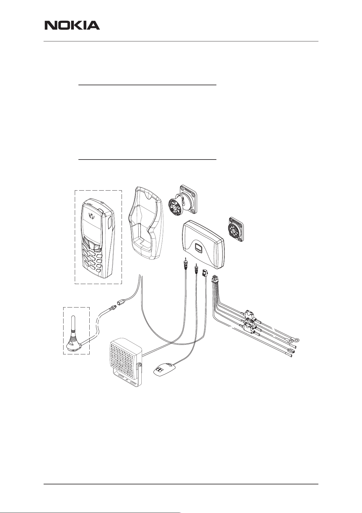
Full Car Kit CARK132 Option
The CARK132 includes the following parts:
Advanced Active Car Holder MCC–5
Advanced HF Unit HFU–5
Power Cable PCH–4J
Mounting Plate MKU–1
Swivel Mount HHS–9
HF Microphone HFM–8
HF Speaker HFS–12
NPM–9
General Information
HHS-9
AMD–2
HFS–12
MCC-5
MKU–1
HFU-5
PCH-4J
HFM-8
Please, note that the items enclosed in broken-line (phone & antenna) are not supplied with CARK132. The external antenna AMD–2 is recommended.
Issue 1 02/2002
Nokia Corporation
Page 5
Page 12
NPM–9
General Information
Product and Module List
Unit/type:
NPM–9 Transceiver
BLB–2 Standard Battery Li–ion
ACP–7E Standard Charger (EUR) 207–253 Vac
ACP–7U Standard Charger (US) 108–132 Vac
ACP–7C Standard Charger (US) 198–242 Vac
ACP–7X Standard Charger (UK) 207–253 Vac
ACP–7H Standard Charger (UK) 180–220 Vac
ACP–7A Standard Charger (AUS) 216–264 Vac
ACP–8E Travel Charger (EUR) 90–264 Vac
ACP–8K Travel Charger (Korea) 90–264 Vac
ACP–8X Travel Charger (UK) 90–264 Vac
PAMS Technical Documentation
ACP–8U Travel Charger (US) 90–264 Vac
ACP–8C Travel Charger (China) 90–264 Vac
ACP–8A Travel Charger (Australia) 90–264 Vac
LCH–9 Mobile Charger
PPH–1 Plug–in HF Car Kit
MBD–10 Mobile Holder
MKU–1 Mounting Plate
HHS–9 Swivel Mount
DCD–1 Desktop Stand
DDC–1 Battery Charging Stand
HFM–8 HF Microphone
HDD–1 Headset
HDC–5 Headset
HDE–2 Headset
HDB–5 Boom Headset
LPS–3 Loopset
Page 6
HFU–5 Advanced HF Unit
MCC–5 Advanced Active Car Holder
PCH–4J Power Cable
HFS–12 HF Speaker
Nokia Corporation
Issue 1 02/2002
Page 13
PAMS Technical Documentation
General Information
General Specifications of Transceiver NPM–9
Parameter Unit
Cellular system GSM900 and GSM1800
RX frequency band EGSM: 925 ... 935 MHz
GSM900 935 ... 960 MHz
GSM1800 1805 ... 1880 MHz
TX frequency band EGSM 880 ... 890 MHz
GSM900 890 ... 915 MHz
GSM1800 1710 ... 1785 MHz
Output power GSM900 * +5 ...+33 dBm / 3.2 mW ... 2 W
GSM1800 +0 ...+30 dBm / 1.0 mW ... 1 W
Duplex spacing GSM900 * 45 MHz GSM1800 95 MHz
Number of RF channels EGSM 50
GSM900 124
GSM1800 374
Channel spacing 200 kHz
NPM–9
Number of TX power levels GSM900 * 15 GSM1800 16
Sensitivity, static channel GSM900: –102 dBm
GSM1800: –102 dBm (norm. cond. only)
Frequency error, static channel < 0.1 ppm
RMS phase error < 5.0
Peak phase error < 20.0
*) applies also to EGSM
o
o
Issue 1 02/2002
Nokia Corporation
Page 7
Page 14

NPM–9
General Information
PAMS Technical Documentation
This page intentionally left blank.
Page 8
Nokia Corporation
Issue 1 02/2002
Page 15

PAMS Technical Documentation
NPM–9 Series Transceivers
System Module & UI
Issue 1 02/2002 Nokia Corporation
Page 16

NPM–9
System Module & UI
PAMS Technical Documentation
CONTENTS
Transceiver NPM–9 5. . . . . . . . . . . . . . . . . . . . . . . . . . . . . . . . . . . . .
Introduction 5. . . . . . . . . . . . . . . . . . . . . . . . . . . . . . . . . . . . . . . . . .
Electrical Modules 5. . . . . . . . . . . . . . . . . . . . . . . . . . . . . . . . . .
Operation Modes 6. . . . . . . . . . . . . . . . . . . . . . . . . . . . . . . . . . .
Interconnection Diagram 6. . . . . . . . . . . . . . . . . . . . . . . . . . . . . .
System Module LA5 7. . . . . . . . . . . . . . . . . . . . . . . . . . . . . . . . . . . . .
Baseband Module 7. . . . . . . . . . . . . . . . . . . . . . . . . . . . . . . . . . . .
Block Diagram 7. . . . . . . . . . . . . . . . . . . . . . . . . . . . . . . . . . . . .
Technical Summary 8. . . . . . . . . . . . . . . . . . . . . . . . . . . . . . . .
DC Characteristics 9. . . . . . . . . . . . . . . . . . . . . . . . . . . . . . . . .
Regulators and Supply Voltage Ranges 9. . . . . . . . . . . . .
External and Internal Signals and Connections 10. . . . . . . . .
Internal Signals and Connections 10. . . . . . . . . . . . . . . . . . . . .
FM Radio Interface 10. . . . . . . . . . . . . . . . . . . . . . . . . . . . . . .
Internal microphone 11. . . . . . . . . . . . . . . . . . . . . . . . . . . . . .
Internal speaker 11. . . . . . . . . . . . . . . . . . . . . . . . . . . . . . . . .
AC and DC Characteristics of RF–BB voltage supplies 12
AC and DC Characteristics of RF–BB digital signals 13. .
AC and DC Characteristics of RF–BB analogue signals 14
External Signals and Connections 15. . . . . . . . . . . . . . . . . . . .
UI (board–to–board) connector 15. . . . . . . . . . . . . . . . . . . .
LCD connector 16. . . . . . . . . . . . . . . . . . . . . . . . . . . . . . . . . .
DC connector 17. . . . . . . . . . . . . . . . . . . . . . . . . . . . . . . . . . .
Headset connector 17. . . . . . . . . . . . . . . . . . . . . . . . . . . . . . .
SIM connector 18. . . . . . . . . . . . . . . . . . . . . . . . . . . . . . . . . . .
Functional Description 19. . . . . . . . . . . . . . . . . . . . . . . . . . . . . .
Modes of Operation 19. . . . . . . . . . . . . . . . . . . . . . . . . . . . . . . .
Supply Voltage Regulation 20. . . . . . . . . . . . . . . . . . . . . . . . . .
Battery 21. . . . . . . . . . . . . . . . . . . . . . . . . . . . . . . . . . . . . . . . . . . .
Power Up and Reset 21. . . . . . . . . . . . . . . . . . . . . . . . . . . . . . .
A/D Channels 22. . . . . . . . . . . . . . . . . . . . . . . . . . . . . . . . . . . . . .
FM Radio 23. . . . . . . . . . . . . . . . . . . . . . . . . . . . . . . . . . . . . . . . .
IR Module 24. . . . . . . . . . . . . . . . . . . . . . . . . . . . . . . . . . . . . . . . .
Backup Battery 24. . . . . . . . . . . . . . . . . . . . . . . . . . . . . . . . . . . .
SIM Interface 24. . . . . . . . . . . . . . . . . . . . . . . . . . . . . . . . . . . . . .
Buzzer 25. . . . . . . . . . . . . . . . . . . . . . . . . . . . . . . . . . . . . . . . . . . .
Internal Microphone 25. . . . . . . . . . . . . . . . . . . . . . . . . . . . . . . .
UPP 26. . . . . . . . . . . . . . . . . . . . . . . . . . . . . . . . . . . . . . . . . . . . . .
Memory Block 26. . . . . . . . . . . . . . . . . . . . . . . . . . . . . . . . . . . . .
RF Module 28. . . . . . . . . . . . . . . . . . . . . . . . . . . . . . . . . . . . . . . . . .
RF Frequency Plan 28. . . . . . . . . . . . . . . . . . . . . . . . . . . . . . . . .
DC characteristics 29. . . . . . . . . . . . . . . . . . . . . . . . . . . . . . . . . .
Regulators 29. . . . . . . . . . . . . . . . . . . . . . . . . . . . . . . . . . . . . .
Power Distribution Diagram 30. . . . . . . . . . . . . . . . . . . . . . . . . .
Page 2
Nokia Corporation
Issue 1 02/2002
Page 17

NPM–9
PAMS Technical Documentation
RF characteristics 31. . . . . . . . . . . . . . . . . . . . . . . . . . . . . . . . . .
Transmitter characteristics 31. . . . . . . . . . . . . . . . . . . . . . . .
Receiver characteristics 31. . . . . . . . . . . . . . . . . . . . . . . . . .
RF Block Diagram 32. . . . . . . . . . . . . . . . . . . . . . . . . . . . . . . . . .
Frequency synthesizers 33. . . . . . . . . . . . . . . . . . . . . . . . . . . . .
Receiver 34. . . . . . . . . . . . . . . . . . . . . . . . . . . . . . . . . . . . . . . . . .
Transmitter 35. . . . . . . . . . . . . . . . . . . . . . . . . . . . . . . . . . . . . . . .
AFC function 35. . . . . . . . . . . . . . . . . . . . . . . . . . . . . . . . . . . . . .
DC–compensation 36. . . . . . . . . . . . . . . . . . . . . . . . . . . . . . . . .
UI Board LU9 37. . . . . . . . . . . . . . . . . . . . . . . . . . . . . . . . . . . . . . . .
LCD & Keypad Illumination 37. . . . . . . . . . . . . . . . . . . . . . . . . .
Internal Speaker 38. . . . . . . . . . . . . . . . . . . . . . . . . . . . . . . . . . .
Schematic Diagrams (at the back of the binder): LA5 layout 01 and LU9 layout 11
RF & BB (Version 0.0 Edit 2) for layout version 01 A–1. . . . . . . . . .
RF (Version 2.0 Edit 2) for layout version 01 A–2. . . . . . . . . . . . . . .
System Module & UI
BB Connections (Version 0.0 Edit 4) for layout version 01 A–3. . . .
System Connector (Version 1.3 Edit 162) for layout version 01 A–4
Audio Interface (Version 1.3 Edit 1) for layout version 01 A–5. . . .
UEM of BB (Version 2.0 Edit 1) for layout version 01 A–6. . . . . . . . .
Light Filtering (Version 2.0 Edit ) for layout version 01 A–7. . . . . .
Display and Keyboard Interface (Version 1.3 Edit 212) for layout version 01A–8
Infrared Module (Version 2.0 Edit 38) for layout version 01 A–9. .
FM Radio (Version 1.3 Edit 110) for layout version 01 A–10. . . . . . .
SIM Reader (Version 1.3 Edit 48) for layout version 01 A–11. . . . . .
UPP and decoupling capacitors (Version 2.0 Edit 91) for layout version 01A–12
Discrete capacitors for UPP (Version 1.3 Edit 10) for layout version 01 A–13
GSM RF – BB Interface (Version 1.3 Edit 35) for layout version 01 A–14
Flash Memory (Version 2.0 Edit 35) for layout version 01 A–15. . . .
Discrete capacitors for memory without VFlash1 (V. 1.3 Edit 10) layout 01A–16
Test pattern – 5 pin (Version 2.0 Edit 12) for layout version 01 A–17
Layout Diagram of LA5 – Top (Version 01) A–18. . . . . . . . . . . . . . . . .
Layout Diagram of LA5 – Bottom (Version 01) A–18. . . . . . . . . . . . . .
Testpoints of LA5 – Top (Version xx) A–19. . . . . . . . . . . . . . . . . . . . . . .
Testpoints of LA5 – Bottom (Version 01) A–19. . . . . . . . . . . . . . . . . . .
UI Board – LU9 for version 11 A–20. . . . . . . . . . . . . . . . . . . . . . . . . . . .
Layout Diagram – LU9 for version 11 A–21. . . . . . . . . . . . . . . . . . . . . .
Issue 1 02/2002
Nokia Corporation
Page 3
Page 18

NPM–9
System Module & UI
PAMS Technical Documentation
This page intentionally left blank.
Page 4
Nokia Corporation
Issue 1 02/2002
Page 19

PAMS Technical Documentation
Transceiver NPM–9
Introduction
The NPM–9 is a dual band radio transceiver unit for the E–GSM900 and
GSM1800 networks. GSM power class is 4 and GSM1800 power class is
1. It is a true 3 V transceiver, with an internal antenna and vibra.
The NPM–9 phone includes integrated FM radio. Radio is used as a nor-
mal mono receiver. FM radio is highly integrated. Only few external com-
ponents are needed. Headset is used as an antenna for radio.
The transceiver has a full graphic display and the user interface is based
on a Jack style UI with two soft keys.
An internal antenna is used, there is no connection to an external anten-
na.
The transceiver has a low leakage tolerant earpiece and an omnidirec-
tional microphone, providing an excellent audio quality. The transceiver
supports a full rate, an enhanced full rate and a half rate speech decod-
ing.
NPM–9
System Module & UI
An integrated IR link provides a connection between two NPM–9 trans-
ceivers or a transceiver and a PC (internal data), or a transceiver and a
printer.
The small SIM ( Subscriber Identity Module ) card is located under the
battery. SIM interface supports both 1.8V and 3V SIM cards.
Electrical Modules
The radio module consists of Radio Frequency (RF) and baseband (BB).
User Interface (UI) contains display, keyboard, IR link, vibra, HF/HS con-
nector and audio parts. UI is divided into radio PWB LA5 and UI PWB
LU9. FM radio is located on the main PWB.
The electrical part of the keyboard is located in separate UI PWB named
LU9. LU9 is connected to radio PWB through spring connectors.
The System blocks provide the MCU, DSP, external memory interface
and digital control functions in UPP ASIC (Universal Phone Processor).
Power supply circuitry, charging, audio processing and RF control hard-
ware are in UEM ASIC (Universal Energy Management).
The purpose of the RF block is to receive and demodulate the radio fre-
quency signal from the base station and to transmit a modulated RF sig-
nal to the base station.
Issue 1 02/2002
Nokia Corporation
Page 5
Page 20
NPM–9
System Module & UI
Operation Modes
The transceiver has six different operation modes:
– power off mode – idle mode
– active mode – charge mode
– local mode – test mode
In the power off mode circuits are powered down and only sleep clock is
running.
In the idle mode only the circuits needed for power up are supplied.
In the active mode all the circuits are supplied with power although some
parts might be in the idle state part of the time.
The charge mode is effective in parallel with all previous modes. The
charge mode itself consists of two different states, i.e. the fast charge and
the maintenance mode.
The local and test modes are used for alignment and testing.
PAMS Technical Documentation
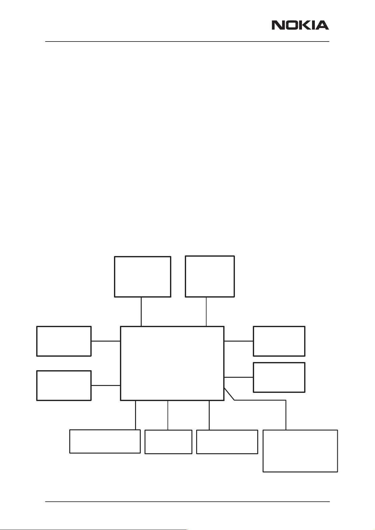
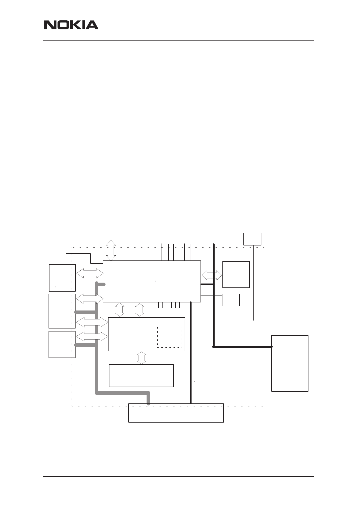
Interconnection Diagram
Keyboard
module
SIM Battery
Radio
Module
LA5
Antenna
Display
Charger
Page 6
MIC
IR Link
Nokia Corporation
Earpiece
HF
+
FM antenna
Issue 1 02/2002
Page 21
PAMS Technical Documentation
System Module LA5
Baseband Module
The baseband architecture supports a power saving function called ”sleep
mode”. This sleep mode shuts off the VCTCXO, which is used as system
clock source for both RF and baseband. During the sleep mode the sys-
tem runs from a 32 kHz crystal. The phone is waken up by a timer run-
ning from this 32 kHz clock supply. The sleep time is determined by net-
work parameters. Sleep mode is entered when both the MCU and the
DSP are in standby mode and the normal VCTCXO clock is switched off.
NPM–9 supports both three and two wire type of Nokia chargers. Three
wire chargers are treated like two wire ones. There is not separate PWM
output for controlling charger but it is connected to GND inside the bottom
connector. Charging is controlled by UEM ASIC (Universal Energy Man-
agement) and EM SW running in the UPP (Universal Phone Processor).
NPM–9
System Module & UI
BLB–2 Li–ion battery is used as main power source for the phone.
Block Diagram
TX/RX SIGNALS
PWR
IR
FM
radio
UI
Digital Control
UPP
FLASH MEMORY
RF SUPPLIES
UEM
BB SUPPLIES
RAM
PA SUPPL Y
32kHz
CLK
SLEEP CLOCK
SIM
VBAT
13MHz
CLK
SYSTEM CLOCK
BATTERY
BASEBAND
UPP ASIC (Universal Phone Processor) provides the MCU, DSP, external
memory interface and digital control functions. UEM ASIC (Universal En-
ergy Management) contains power supply circuitry, charging, audio proc-
essing and RF control hardware.
Issue 1 02/2002
EXT. AUDIO
HS–connector
Charger
connector
Nokia Corporation
Page 7
Page 22

NPM–9
System Module & UI
Technical Summary
Baseband is running from power rails 2.8V analog voltage and 1.8V I/O
voltage. UPP core voltage Vcore can be lowered down to 1.0V, 1.3V and
1.5V. UEM includes 6 linear LDO (low drop–out) regulators for baseband
and 7 regulators for RF. It also includes 4 current sources for biasing pur-
poses and internal usage. UEM also includes SIM interface which has
supports both 1.8V and 3V SIM cards.
Note: 5V SIM cards are no longer supported by NPM–9 baseband.
A real time clock function is integrated into the UEM which utilizes the
same 32kHz clock supply as the sleep clock. A backup power supply is
provided for the RTC which keeps the real time clock running when the
main battery is removed. The backup power supply is a rechargeable sur-
face mounted capacitor. The backup time with the capacitor is 30 minutes
minimum.
The analog interface between the baseband and the RF section is han-
dled by a UEM ASIC. UEM provides A/D and D/A conversion of the in–
phase and quadrature receive and transmit signal paths and also A/D and
D/A conversions of received and transmitted audio signals to and from
the user interface. The UEM supplies the analog TXC and AFC signals to
RF section according to the UPP DSP digital control. Data transmission
between the UEM and the UPP is implemented using two serial busses,
DBUS for DSP and CBUS for MCU. RF ASIC, Hagar, is controlled
through UPP RFBUS serial interface. There is also separate signals for
PDM coded audio. Digital speech processing is handled by the DSP in-
side UPP ASIC. UEM is a dual voltage circuit, the digital parts are running
from the baseband supply 1.8V and the analog parts are running from the
analog supply 2.78V also VBAT is directly used by some blocks.
PAMS Technical Documentation
The baseband supports both internal and external microphone inputs and
speaker outputs. UEM also includes third microphone input which is used
in NPM–9 for FM radio. Input and output signal source selection and gain
control is done by the UEM according to control messages from the UPP.
Keypad tones, DTMF, and other audio tones are generated and encoded
by the UPP and transmitted to the UEM for decoding. A buzzer and exter-
nal vibra alert control signals are generated by the UEM with separate
PWM outputs.
NPM–9 has two external serial control interfaces: FBUS and MBUS.
These busses can be accessed only through production test pattern.
EMC shielding for baseband is implemented using a metallized plastic
frame and UI PWB ground plane. On the other side the engine is shielded
with PWB grounding. Heat generated by the circuitry will be conducted
out via the PWB ground planes.
NPM–9 radio module is implemented to 8 layer PWB. UI module is divid-
ed between main PWB LA5 and separate UI PWB LU9.
Page 8
Nokia Corporation
Issue 1 02/2002
Page 23
PAMS Technical Documentation
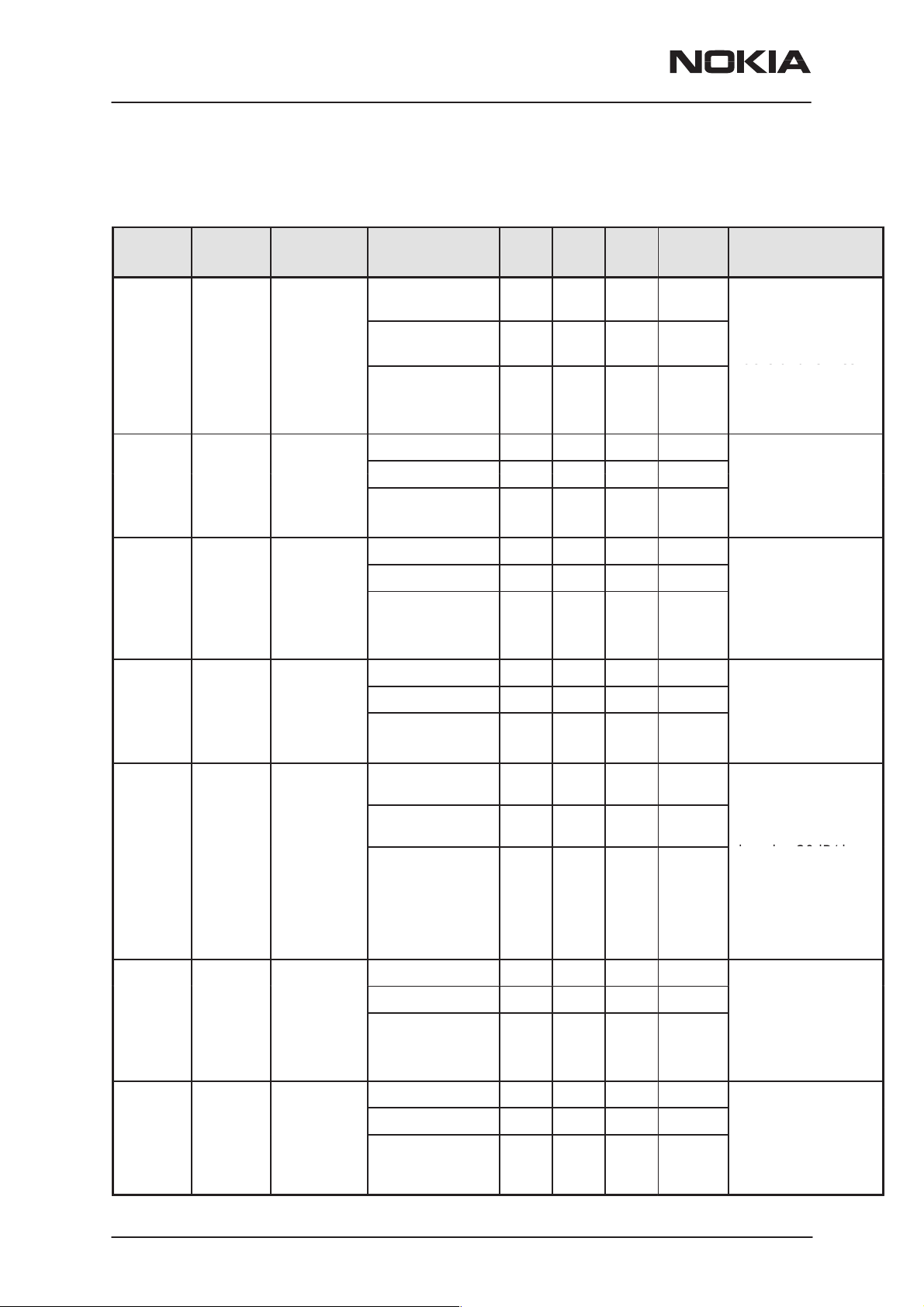
DC Characteristics
Regulators and Supply Voltage Ranges
Battery Voltage Range
Signal Min Nom Max Note
NPM–9
System Module & UI
VBAT 3.1V 3.6V 4.2V (charging
high limit voltage)
BB Regulators
Signal Min Nom Max Note
VANA 2.70V 2.78V 2.86V I
VFLASH1 2.70V 2.78V 2.86V I
VFLASH2 2.70V 2.78V 2.86V I
VSIM 1.745V
2.91V
1.8V
3.0V
1.855V
3.09V
VIO 1.72V 1.8V 1.88V I
VCORE 1.0V
1.235V
1.425V
1.710V
1.053V
1.3V
1.5V
1.8V
1.106V
1.365V
1.575V
1.890V
RF Regulators
3.1V SW cut off
= 80mA
max
= 70mA
max
I
= 1.5mA
Sleep
= 40mA
max
I
= 25mA
max
I
= 0.5mA
Sleep
= 150mA
max
I
= 0.5mA
Sleep
I
= 200mA
max
I
= 0.2mA
Sleep
Default value =
1.5V
Signal Min Nom Max Note
VR1A 4.6V 4.75V 4.9V I
VR2 2.70V
3.20V
2.78V
3.3V
2.86V
3.40V
VR3 2.70V 2.78V 2.86V I
VR4 2.70V 2.78V 2.86V I
VR5 2.70V 2.78V 2.86V I
VR6 2.70V 2.78V 2.86V I
VR7 2.70V 2.78V 2.86V I
max
I
max
max
max
I
Sleep
max
I
Sleep
max
I
Sleep
max
= 10mA
= 100mA
= 20mA
= 50mA
= 0.1mA
= 50mA
= 0.1mA
= 50mA
= 0.1mA
= 45mA
Issue 1 02/2002
Nokia Corporation
Page 9
Page 24
NPM–9
System Module & UI
PAMS Technical Documentation
External and Internal Signals and Connections
This section describes the external and internal electrical connection and
interface levels on the baseband. The electrical interface specifications
are collected into tables that covers a connector or a defined interface.
Internal Signals and Connections
FM Radio Interface
BB Signal FM Radio
Signal
VFLASH2
GenIO(3) FMClk
GenIO(8) FMWrEn
Vcc1 2.7V 2.78V 2.86V max. Icc1
Vcc2 2.7V 2.78V 2.86V max. Icc2
VDD 2.7V 2.78V 2.86V max. IDD
Min Nom Max Condition Note
19mA
800uA
3mA
1.4V
0
30ppm Stability
1.4V
0V
20µs t
1.8V 1.88V
0.4V
75581 kHz Frequency In GSM
2 µs t
1.8V 1.88V
0.4V
High
Low
rise
High
Low
wd
Reference
clock for FM
radio module
rise / fall time
FMWrEn
before rising
edge of
FMCtrlClk
(write operation)
high
GenIO(11) FMCtrlClk
Page 10
1.4V
0
50 ms t
1.8V 1.88V
0.4V
1 µs tr / t
Nokia Corporation
High
Low
start
max. 300kHz
f
rise / fall time
FMCtrlClk
delay after
switching on
the VFLASH2
(oscillator running)
Issue 1 02/2002
Page 25
PAMS Technical Documentation
out ut
NPM–9
System Module & UI
BB Signal
Signal
GenIO(12) FMCtrlDa
1.4V
0
10 µs t
1.5 µs t
GenIO(27) FMTuneX 1.4V
0
1.8V 1.88V
0.4V
14us t
1.8V 1.88V
0.4V
High
Low
da
shift
hold
High
Low
NoteConditionMaxNomMinFM Radio
Bidirectional
shift register
available after
”search
ready”
data available
after
FMCtrlClk
rising edge (read
operation)
FMCtrlDa
sta-
bile after
FMCtrlClk
rising edge
(write operation)
from FM module to UPP
(FMCtrlClk =
’1’)
MIC3P FMAudio
228mV
pp
326mV
pp
460mV
pp
50dB S/N
2% Harmonic
Internal microphone
Signal Min Nom Max Condition Note
MICP
200mV
pp
2.0 V 2.1 V 2.25 V DC
MICN 2.0V 2.1V 2.25V DC
Internal speaker
Signal Min Nom Max Condition Note
EARP
0.75V 0.8V
EARN
0.75V 0.8V
2.0 V
0.85V
2.0 V
0.85V
pp
pp
distortion
AC
AC
DC
AC
DC
2.2kΩ to
MIC1B
Differential
p
(V
= 4.0
diff
Vpp)
Issue 1 02/2002
Nokia Corporation
Page 11
Page 26
NPM–9
04V
tracks and ferrites
f
CO
Current
2 10
mA
tu
tuning
Su
Su ly for TX
VLO
buffers, rescaler
System Module & UI
PAMS Technical Documentation
AC and DC Characteristics of RF–BB voltage supplies
Signal
name
VBAT Battery P A & UEM
VR1A UEM VCP
VR2 UEM VRF_TX
VR3 UEM VCTCXO
From To Parameter Min Typ Max Unit Function
Voltage 2.95 3.6 4.2 V
Current 2000 mA
Current drawn by
PA when ”off”
Voltage 4.6 4.75 4.9 V
Noise density 240 nVrms/
Voltage 2.70 2.78 2.86 V
Current 65 100 mA
Noise density
f=100Hz
f>300Hz
Voltage 2.70 2.78 2.86 V
0.8 2 uA
sqrt(Hz)
120 nVrms/
sqrt(Hz)
Battery supply .
Cut–off level of
regulators is 3.
Losses in pwb
tracks and ferrites
are taken account to
minimum battery
voltage level.
Supply for varactor
or UHF V
ning.
.
Supply for part of
transmit strip.
pply for TX
I/Q–modulators.
Supply for VCTCXO
.
VR4 UEM VRF_RX
VR5 UEM VDIG,
VPRE,
VL
VR6 UEM VBB
Current 1 20 mA
Noise density 240 nVrms/
sqrt(Hz)
Voltage 2.70 2.78 2.86 V
Current 50 mA
Noise density
f = 6 Hz
f = 60 Hz
f 600Hz
Voltage 2.70 2.78 2.86 V
Current 50 mA
Noise density
BW=100Hz...
100kHZ
Voltage 2.70 2.78 2.86 V
Current 50 mA
Noise density
BW=100Hz...
100kHz
5500
240 nVrms/
240 nVrms/
550
55
nVrms/
sqrt(Hz)
sqrt(Hz)
sqrt(Hz)
Supply for Hagar
RX; preamp., mixer,
DTOS
Noise density
decades 20dB/dec
from 6Hz to 600Hz.
From f >600Hz
maximum noise
density
RMS
/√Hz.
l
r
,
55nV
Supply for Hagar
PLL; dividers, LO–
ffr pr
Supply for Hagar
BB and LNA
Page 12
Nokia Corporation
Issue 1 02/2002
Page 27
PAMS Technical Documentation
CO
for RF–IC
density is
some digita
some digital arts of
Signal name
FromToParameter
Fun
ter
DC
ng?
name
VR7 UEM UHF VCO
System Module & UI
Voltage 2.70 2.78 2.86 V
Current 30 mA
NPM–9
FunctionUnitMaxTypMinParameterToFromSignal
Supply for UHF
V
VrefRF01 UEM VREF_RX
VrefRF02 UEM VB_EXT
Noise density
100Hz<f<2kHz
2kHz<f<10kHz
10kHz<f<30kHz
30kHz<f<90kHz
90kHz<f<3MHz
Voltage 1.334 1.35 1.366 V
Current 100 uA
Temp Coef –65 +65 uV/C
Noise density
BW=600Hz...
100kHz Note
Voltage 1.323 1.35 1.377 V
Current 100 uA
Temp Coef –65 +65 uV/C
Noise density
BW=100Hz...
100kHz
70
nVrms/
55
sqrt(Hz)
35
30
30
60 nVrms/
sqrt(Hz)
350 nVrms/
sqrt(Hz)
Voltage Reference
.
Note: Below
600Hz noise
allowed to
increase 20
dB/oct
Supply for RF–BB
digital interface and
l parts of
RF.
AC and DC Characteristics of RF–BB digital signals
Min Typ Max Unit
TXP
(RFGenOut3)
UPP PA &
RF–IC
”1” 1.38 1.88 V
”0” 0 0.4 V
Load Resistance 10 220 kohm
Load Capacitance 20 pF
Timing Accuracy 1/4 symbol
Input Characteristics
c-
tion
Tran
smit
ter
pow
er
amp
lifier
ena
ble /
N2
timi
??
Issue 1 02/2002
Nokia Corporation
Page 13
Page 28
NPM–9
ena
ena
data
data
d
cloc
cloc
(G
)
ag
Hag
circuits, AC
circuits, AC
System Module & UI
PAMS Technical Documentation
RFBusEna1X UPP RF–IC
RFBusData UPP RF–IC
RFBusClk UPP RF–IC
ParameterToFromSignal name
UnitMaxTypMin
”1” 1.38 1.88 V
”0” 0 0.4 V
Current 50 uA
Load resistance 10 220 kohm
Load capacitance 20 pF
”1” 1.38 1.88 V
”0” 0 0.4 V
Load resistance 10 220 kohm
Load capacitance 20 pF
Data frequency 10 MHz
”1” 1.38 1.88 V
”0” 0 0.4 V
Load resistance 10 220 kohm
Load capacitance 20 pF
Data frequency 10 MHz
Fun
c-
tion
RFb
us
ble
RFb
us
;
rea
/writ
e
RFb
us
k
RESET
ENIO6
UPP RF–IC
”1” 1.38 1.85 V
”0” 0 0.4 V
Load capacitance 20 pF
Load resistance 10 220 kohm
Timing accuracy 1/4 symbol
Res
et to
H
ar
AC and DC Characteristics of RF–BB analogue signals
Signal name From To Parameter Min Typ Max Unit Function
VCTCXO VCTCXO UPP
VCTCXOGnd VCTXO UPP DC Level 0 V Ground for
Signal amplitude 0.2 0.8 2.0 Vpp
Input Impedance 10 kohm
Input Capacitance 10 pF
Harmonic Content –8 dBc
Clear signal
window (no glitch)
Duty Cycle 40 60 %
200 mVpp
High stability clock
signal for the logic
coupled. Distorted
sine wave eg.
sawtooth.
reference clock
RXI/RXQ RF–IC UEM
Page 14
Nokia Corporation
Differential voltage
swing (static)
DC level 1.3 1.35 1.4 V
I/Q amplitude
missmatch
I/Q phase
missmatch
1.35 1.4 1.45 Vpp
0.2 dB
–5 5 deg
Issue 1 02/2002
RX baseband
signal.
Page 29
PAMS Technical Documentation
Programmable
voltage
opa
oam G1
NPM–9
System Module & UI
FunctionUnitMaxTypMinParameterToFromSignal name
TXIP / TXIN UEM RF–IC
TXQP /
TXQN
AFC UEM VCTCXO
Aux_DAC
(TxC)
UEM RF–IC Same spec as for TXIP / TXIN Differential
UEM RF
Differential voltage
swing (static)
DC level 1.17 1.20 1.23 V
Source
Impedance
Voltage Min
Max
Resolution 11 bits
Load resistance
and capacitance
Step settling time 0.2 ms
Voltage Min
Max 2.4
Source
Impedance
Resolution 10 bits
2.23 2.48 Vpp
200 ohm
0.0
2.4
1
0.1
V
2.6
kohm
100
nF
0.1 V
200 ohm
Programmable
voltage swing.
common mode
.
Between
TXIP–TXIN
quadrature phase
TX baseband
signal for the RF
modulator
Automatic
frequency control
signal for
VCTCXO
Transmitter power
control
Noise density
BW=100Hz...
100kHz
Temp Coef –65 +65 uV/C
RFTemp RF UEM
Vbase RF UEM Voltage 2.7 V Detected voltage
Voltage at –20oC 1,57
Voltage at +25oC 1,7
Voltage at +60oC 1,79
800 nVrms/
sqrt(Hz)
V Temperature
NOTE; Assumed
power control
mp G=1
sensor of RF.
from PA power
level sensing unit
External Signals and Connections
UI (board–to–board) connector
Pin Signal Min Nom Max Condition Note
1 SLOWAD(2) 1.5V
0.1V
2 VBAT 3.0V 3.6V 4.2V Battery voltage
3 ROW(4) 0.7xVIO
0
2.7V
1.0V
1.8V
0.3xVIO
Flip closed
Flip open
High
Low
used for flip
identification
for leds
Keyboard ma-
trix row 4
Issue 1 02/2002
Nokia Corporation
Page 15
Page 30
NPM–9
System Module & UI
PAMS Technical Documentation
NoteConditionMaxNomMinSignalPin
4 ROW(3) 0.7xVIO
0
5 COL(2) 0.7xVIO
0
6 ROW(2) 0.7xVIO
0
7 COL(1) 0.7xVIO
0
8 ROW(0) 0.7xVIO
0
9 KLIGHT VBAT
10 ROW(1) 0.7xVIO
0
11 COL(3) 0.7xVIO
0
12 COL(4) 0.7xVIO
0
13 GND 0V
14 GND 0V
15 GND 0V
VIO
0.3xVIO
VIO
0.3xVIO
VIO
0.3xVIO
VIO
0.3xVIO
VIO
0.3xVIO
0.3xVBAT
VIO
0.3xVIO
VIO
0.3xVIO
VIO
0.3xVIO
High
Low
High
Low
High
Low
High
Low
High
Low
LED off
LED on
High
Low
High
Low
High
Low
Keyboard matrix row 3
Keyboard matrix column 2
Keyboard matrix row 2
Keyboard matrix column 1
Keyboard matrix row 0
two colour led
control
Keyboard matrix row 1
Keyboard matrix column 3
Keyboard matrix column 4
16 GND 0V
LCD connector
Pin Signal Min Nom Max Condition Note
1 XRES
2 XCS
3 GND 0V
4 SDA
0.8*VIO
0
100ns t
0.8*VIO
0
130ns t
130ns t
300ns t
0.8*VIO
0
0.7*VIO
0
100ns t
100ns t
VIO
0.22*VIO
VIO
0.22*VIO
VIO
0.22*VIO
VIO
0.3*VIO
Logic ’1’
Logic ’0’
rw
Logic ’1’
Logic ’0’
css
csh
csw
Logic ’1’
Logic ’0’
Logic ’1’
Logic ’0’
sds
sdh
Reset
Active low
Reset active
Chip select
Active low
XCS low before
SCLK rising
edge
XCS low after
SCLK rising
edge
XCS high pulse
width
Serial data
(driver input)
Serial data
(driver output)
Data setup time
Data hold time
Page 16
Nokia Corporation
Issue 1 02/2002
Page 31

NPM–9
PAMS Technical Documentation
5 SCLK
6 VDDI (VIO) 1.72V 1.8V 1.88V Logic voltage
7 VDD
(VFLASH1)
8 VOUT 9V Booster output,
0.8*VIO
0
250ns t
1 10ns t
1 10ns t
VIO
0.22*VIO
4.0MHz
Logic ’1’
Logic ’0’
Max frequency
scyc
shw
slw
2.72V 2.78V 2.86V Voltage supply
System Module & UI
NoteConditionMaxNomMinSignalPin
Serial clock input
Clock cycle
Clock high
Clock low
supply
Connected to
VIO
Connected to
VFLASH1
C=1uF connected to GND
DC connector
Pin Signal Min Nom Max Condition Note
2 VCHAR 7.0 V
RMS
8.4 V
RMS
9.2 V
RMS
850 mA
Fast charger
Charger positive input
1 CHGND 0 Charger ground
Headset connector
Pin Signal Min Nom Max Condition Note
5 XMICP
3 XMICN
4 XEARN
7 XEARP
1V
pp
100 mV
2.0 V 2.1 V 2.25 V DC
1V
pp
100 mV
0.75V 0.8V 0.85V DC
1V
pp
0.75V 0.8V 0.85V DC
pp
pp
G = 0dB
G = 20dB
G = 0 dB
G = 20dB
AC
1kΩ to MIC2B
1kΩ to GND
1V
5 HookInt 0V 2.86V
(VFLASH1)
6 HeadInt 0V 2.86V
(VANA)
Issue 1 02/2002
Nokia Corporation
pp
AC
Connected to
UEM AD–converter
Accessory
detection
Page 17
Page 32

NPM–9
System Module & UI
PAMS Technical Documentation
SIM connector
Pin Name Parameter Min Typ Max Unit Notes
1 VSIM
2 SIMRST
3 SIMCLK
4 DATA
1.8V SIM Card 1.6 1.8 1.9
3V SIM Card 2.8 3.0 3.2
1.8V SIM Card 0.9xVSIM
0
3V SIM Card 0.9xVSIM
0
Frequency 3.25 MHz
Trise/Tfall 50 ns
1.8V Voh
1.8V Vol
3 Voh
3 Vol
1.8V Voh
1.8V Vol
3 Voh
3 Vol
1.8V Vih
1.8V Vil
3V Vil
3V Vil
0.9xVSIM
0
0.9xVSIM
0
0.9xVSIM
0
0.9xVSIM
0
0.7xVSIM
0
0.7xVSIM
0
VSIM
0.15xVSIM
VSIM
0.15xVSIM
VSIM
VSIM
VSIM
0.15xVSIM
VSIM
0.15xVSIM
VSIM
0.15xVSIM
VSIM
0.15xVSIM
V Supply voltage
V SIM reset (output)
V
V SIM data (output)
SIM clock
SIM data (input)
Trise/Tfall max 1us
5 NC
6 GND GND 0 V Ground
Page 18
Nokia Corporation
Issue 1 02/2002
Page 33

PAMS Technical Documentation
Functional Description
Modes of Operation
LA5 baseband engine has six different operating modes:
– No supply
– Backup
– Acting Dead
– Active
– Sleep
– Charging
No supply
In NO_SUPPLY mode the phone has no supply voltage. This mode is due
to disconnection of main battery and backup battery or low battery voltage
level in both of the batteries.
Phone is exiting from NO_SUPPLY mode when sufficient battery voltage
level is detected. Battery voltage can rise either by connecting a new bat-
Backup
tery with VBAT > V
tery above V
MSTR+
MSTR+
.
NPM–9
System Module & UI
or by connecting charger and charging the bat-
In BACKUP mode the backup battery has sufficient charge but the main
battery can be disconnected or empty (VBAT < V
VBU
VRTC regulator is disabled in BACKUP mode. VRTC output is supplied
without regulation from backup battery (VBACK). All the other regulators
are disabled.
Acting Dead
If the phone is off when the charger is connected, the phone is powered
on but enters a state called ”Acting Dead”. To the user the phone acts as
if it was switched off. A battery charging alert is given and/or a battery
charging indication on the display is shown to acknowledge the user that
the battery is being charged.
Active
In the active mode the phone is in normal operation, scanning for channels, listening to a base station, transmitting and processing information.
There are several sub–states in the active mode depending on if the
phone is in burst reception, burst transmission, if DSP is working etc.
One of the sub–state of the active mode is FM radio on state. In that case
UEM audio blocks and FM radio are powered on. FM radio circuitry is
controlled by the MCU and 75kHz reference clock is generated in the
UPP. VFLASH2 regulator is operating.
COFF
MSTR
and VBACK >
).
In active mode the RF regulators are controlled by SW writing into UEM’s
registers wanted settings: VR1A can be enabled or disabled. VR2 can be
enabled or disabled and its output voltage can be programmed to be
Issue 1 02/2002
Nokia Corporation
Page 19
Page 34

NPM–9
System Module & UI
2.78V or 3.3V. VR4 –VR7 can be enabled or disabled or forced into low
quiescent current mode. VR3 is always enabled in active mode.
Sleep mode
Sleep mode is entered when both MCU and DSP are in stand–by mode.
Sleep is controlled by both processors. When SLEEPX low signal is detected UEM enters SLEEP mode. VCORE, VIO and VFLASH1 regulators
are put into low quiescent current mode. All RF regulators are disabled in
SLEEP. When SLEEPX=1 is detected UEM enters ACTIVE mode and all
functions are activated.
The sleep mode is exited either by the expiration of a sleep clock counter
in the UEM or by some external interrupt, generated by a charger connection, key press, headset connection etc.
In sleep mode VCTCXO is shut down and 32 kHz sleep clock oscillator is
used as reference clock for the baseband.
Charging
PAMS Technical Documentation
The battery voltage, temperature, size and current are measured by the
UEM controlled by the charging software running in the UPP.
The charging control circuitry (CHACON) inside the UEM controls the
charging current delivered from the charger to the battery. The battery
voltage rise is limited by turning the UEM switch off when the battery voltage has reached 4.2 V. Charging current is monitored by measuring the
voltage drop across a 220 mOhm resistor.
Supply Voltage Regulation
Supply voltage regulation is controlled by UEM asic. There are six separate regulators used by baseband block.
BB Regulators
Signal Min Nom Max Note
VANA 2.70V 2.78V 2.86V I
VFLASH1 2.70V 2.78V 2.86V I
VFLASH2 2.70V 2.78V 2.86V I
VSIM 1.745V
2.91V
VIO 1.72V 1.8V 1.88V I
VCORE 1.0V
1.235V
1.425V
1.710V
1.8V
3.0V
1.053V
1.3V
1.5V
1.8V
1.855V
3.09V
1.106V
1.365V
1.575V
1.890V
= 80mA
max
= 70mA
max
I
= 1.5mA
Sleep
= 40mA
max
I
= 25mA
max
I
= 0.5mA
Sleep
= 150mA
max
I
= 0.5mA
Sleep
I
= 200mA
max
I
= 0.2mA
Sleep
Default value =
1.5V
Page 20
Nokia Corporation
Issue 1 02/2002
Page 35

PAMS Technical Documentation
Battery
Li–ion battery pack BLB–2 is used in NPM–9.
Nominal discharge cut–off voltage 3.1V
Nominal battery voltage 3.6V
Nominal charging voltage 4.2V
Pin numbering of battery pack
Signal name Pin number Function
VBAT 1 Positive battery terminal
BSI 2 Battery capacity measurement (fixed resistor inside the
BTEMP 3 Battery temperature measurement (measured by ntc
GND 4 Negative/common battery terminal
NPM–9
System Module & UI
battery pack)
resistor inside pack)
BLB–2 battery pack pin order
Power Up and Reset
Power up and reset is controlled by the UEM ASIC. NPM–9 baseband
can be powered up in following ways:
1. Press power button which means grounding the PWRONX pin of the
UEM
2. Connect the charger to the charger input
3. Supply battery voltage to the battery pin
4. RTC Alarm, the RTC has been programmed to give an alarm
1 (+)2(BSI)3(BTEMP)4(GND)
After receiving one of the above signals, the UEM counts a 20ms delay
and then enters it’s reset mode. The watchdog starts up, and if the battery
voltage is greater than Vcoff+ a 200ms delay is started to allow references etc. to settle. After this delay elapses the VFLASH1 regulator is enabled. 500us later VR3, VANA, VIO and VCORE are enabled. Finally the
PURX (Power Up Reset) line is held low for 20 ms. This reset, PURX, is
fed to the baseband ASIC UPP, resets are generated for the MCU and
Issue 1 02/2002
Nokia Corporation
Page 21
Page 36

NPM–9
System Module & UI
the DSP. During this reset phase the UEM forces the VCTCXO regulator
on regardless of the status of the sleep control input signal to the UEM.
The FLSRSTx from the ASIC is used to reset the flash during power up
and to put the flash in power down during sleep. All baseband regulators
are switched on at the UEM power on except SIM and VFLASH2 regulators which are controlled by the MCU. The UEM internal watchdogs are
running during the UEM reset state, with the longest watchdog time selected. If the watchdog expires the UEM returns to power off state. The
UEM watchdogs are internally acknowledged at the rising edge of the
PURX signal in order to always give the same watchdog response time to
the MCU.
A/D Channels
The UEM contains the following A/D converter channels that are used for
several measurement purpose. The general slow A/D converter is a 10 bit
converter using the the UEM interface clock for the conversion. An interrupt will be given at the end of the measurement.
PAMS Technical Documentation
The UEM’s 11–channel analog to digital converter is used to monitor
charging functions, battery functions, voltage levels in external accessory
detection inputs, user interface and RF functions.
When the conversion is started the converter input is selected. Then the
signal processing block creates a data with MSB set to ’1’ and and others
to ’0’. In the D/A converter this data controls the switches which connect
the input reference voltage (VrefADC) to the resistor network. The generated output voltage is compared with the input voltage under measurement and if the latter is greater, MSB remains ’1’ else it is set ’0’. The following step is to test the next bit and the next...until LSB is reached. The
result is then stored to ADCR register for UPP to read.
The monitored battery functions are battery voltage (VBATADC), battery
type (BSI) and battery temperature (BTEMP) indication.
The battery type is recognized through a resistive voltage divider. In
phone there is a 100kOhm pull up resistor in the BSI line and the battery
has a pull down resistor in the same line. Depending on the battery type
the pull down resistor value is changed. The battery temperature is measured equivalently except that the battery has a NTC pull down resistor in
the BTEMP line.
KEYB1&2 inputs are used for keyboard scanning purposes. These inputs
are also routed internally to the miscellaneous block. In NPM–9 KEYB1
input is used for flip detection.
Page 22
The HEADINT and HOOKINT are external accessory detection inputs
used for monitoring voltage levels in these inputs. They are routed internally from the miscellaneous block and they are connected to the converter through a 2/1 multiplexer.
The monitored RF functions are PATEMP and VCXOTEMP detection. PATEMP input is used to measure temperature of the RFIC, Hagar. VCXOTEMP is not used in NPM–9.
Nokia Corporation
Issue 1 02/2002
Page 37

PAMS Technical Documentation
FM Radio
FM radio circuitry is implemented using highly integrated radio IC,
TEA5757. Only few external components like filters, discriminator and capacitors are needed.
TEA5757 is an integrated AM/FM stereo radio circuit including digital tuning and control functions. NPM–9 radio is implemented as superheterodyne FM mono receiver. FM stage of the TEA5757 incorporates a tuned
RF stage, a double balanced mixer, one pin oscillator and is designed for
distributed IF ceramic filters. IF frequency is 10.7 MHz.
Channel tuning and other controls are controlled by the MCU. Reference
clock, 75kHz, is generated by the UPP CTSI block.
FM radio circuitry is controlled through serial bus interface by the MCU
SW. TEA5757 informs MCU when channel is tuned by setting
signal to logic ’0’.
Digital Interface
NPM–9
System Module & UI
FMTuneX
UPP TEA5757
GenIO(3)
GenIO(12)
GenIO(11)
GenIO(8)
GenIO(27)
NOTE:
FMCtrlClk
needs to be set to logic ’1’ when data is not written or
FMClk
FMCtrlDa
FMCtrlClk
FMWrEn
FMTuneX
read. This is required for correct operation of the
FM radio audio & antenna connections
Bottom
Connector
1000Ω@100MHz
XTAL
VIO
DATA
BUS–CLK
WR–EN
VIO
MO/ST
FMTuneX
signal.
UEM TEA5757
XEARP
XEARN
Issue 1 02/2002
1n
1n
18pF18pF
72nH
Nokia Corporation
HF
MIC3
HFCM
100nF
3.9nF
4.7kΩ
AFLO
100kΩ
FM_RFI
Page 23
Page 38

NPM–9
System Module & UI
IR Module
The IR interface, when using 2.7V transceiver, is designed into the UEM.
The IR link supports speeds from 9600 bit/s to 1.152 MBit/s up to distance of 1m. Transmission over the IR if half–duplex.
The lenght of the transmitted IR pulse depends on the speed of the transmission. When 230.4 kbit/s or less is used as a transmission speed, pulse
length is maximum 1.63us. If transmission speed is set to 1.152Mbit/s the
pulse length is 154ns according to IrDA specification.
Backup Battery
Backup battery is used in case when main battery is either removed or
discharged. Backup battery is used for keeping real-time clock running for
minimum of 30 minutes.
Rechargeable backup battery is connected between UEM VBACK and
GND. In UEM backup battery charging high limit is set to 3.2V. The cut–
off limit voltage (V
charging is controlled by MCU by writing into UEM register.
BUCoff–
PAMS Technical Documentation
) for backup battery is 2.0V. Backup battery
Polyacene SMD battery type is used. The nominal capacity of the battery
is 0.2 mAh.
SIM Interface
UEM contains the SIM interface logic level shifting. SIM interface can be
programmed to support 3V and 1.8V SIMs. SIM supply voltage is selected by a register in the UEM. It is only allowed to change the SIM supply voltage when the SIM IF is powered down.
The SIM power up/down sequence is generated in the UEM. This means
that the UEM generates the RST signal to the SIM. Also the SIMCardDet
signal is connected to UEM. The card detection is taken from the BSI signal, which detects the removal of the battery. The monitoring of the BSI
signal is done by a comparator inside UEM. The comparator offset is
such that the comparator output do not alter state as long as the battery
is connected. The threshold voltage is calculated from the battery size
specifications.
The SIM interface is powered up when the SIMCardDet signal indicates
”card in”. This signal is derived from the BSI signal.
Parameter Variable Min Typ Max Unit
SIMCARDet, BSI comparator Threshold Vkey 1.94 2.1 2.26 V
SIMCARDet, BSI comparator Hysteresis (1) Vsimhyst 50 75 100 mV
The whole SIM interface locates in two chip UPP and UEM.
The SIM interface in the UEM contains power up/down, port gating, card
detect, data receiving, ATR–counter, registers and level shifting buffers
logic. The SIM interface is the electrical interface between the Subscriber
Identity Module Card (SIM Card) and mobile phone (via UEM device).
Page 24
Nokia Corporation
Issue 1 02/2002
Page 39

PAMS Technical Documentation
The data communication between the card and the phone is asynchronous half duplex. The clock supplied to the card is in GSM system 1.083
MHz or 3.25 MHz. The data baud rate is SIM card clock frequency divided by 372 (by default), 64, 32 or 16. The protocol type, that is supported, is T=0 (asynchronous half duplex character transmission as defined in ISO 7816–3).
NPM–9
System Module & UI
SIM
C5 C6 C7
C1C2C3
From Battery Type contact
C8
C4
The internal clock frequency from UPP CTSI block is 13 MHz in GSM.
Thus to achieve the minimum starting SIMCardClk rate of 3.25 MHz (as is
required by the authentication procedure and the duty cycle requirement
of between 40% and 60%) then the slowest possible clock supplied to the
SIM has to be in the GSM system clock rate of 13/4 MHz.
SIMDATA
SIMCLK
VSIM
BSI
SIMRST
GND
UEM
SIMIF
register
SIMIO
SIMClk
Data
UEM
digital
logic
GND
SIMIO
SIMClk
Data
UPP
UIF Block
UEMInt
CBusDa
CBusEnX
CBusClk
Buzzer
Buzzer is used to generate alerting tones and melodies to indicate incoming call. It is also used to generate keypress and warning tones for the
user. Buzzer is controlled by PWM (Pulse Width Modulation) signal generated by the buzzer driver of the UEM. Target SPL is 100dB (A) at 5cm.
Internal Microphone
The internal microphone capsule is mounted in the bottom connector. Microphone is omnidirectional. The internal microphone is connected to the
UEM microphone input MIC1P/N. The microphone input is asymmetric
and microphone bias is provided by the UEM MIC1B. The microphone
input on the UEM is ESD protected. Spring contacts are used to connect
the microphone contacts to the main PWB.
Issue 1 02/2002
Nokia Corporation
Page 25
Page 40

NPM–9
System Module & UI
UEM
MIC1B
MIC1N
PAMS Technical Documentation
22pF 100nF
33nF
2k2
UPP
33nF
MIC1P
2k2
600Ω@100MHz
27pF
22pF
UPP (Universal Phone Processor) is the digital ASIC of the baseband.
UPP includes 8MBit internal RAM, ARM7 Thump 16/32–bit RISC MCU
core, LEAD3 16–bit DSP core, ROM for MCU boot code and all digital
control logic.
Main functions of the custom logic are:
1. Interface between system logic and MCU/DSP (BodyIf)
2. Clocking, timing, sleep and interrupt block (CTSI) for system
timing control
3. MCU controlled general purpose USART, MBUS USART and
general purpose IOs (PUP).
4. SIM card interface (SIMIf)
5. GSM coder (Coder)
6. GPRS support (GPRSCip)
7. Interfaces for keyboard, LCD and UEM (UIF)
8. Accessory interface for IrDA SIR, IrDA FIR and LPRF (AccIf)
9. SW programmable RF interface (MFI)
10. Programmable serial interface for Hagar RFIC (SCU)
11. Test interface (TestIf)
Memory Block
For the MCU UPP includes ROM, 2 kbytes, that is used mainly for boot
code of MCU. To speed up the MCU operation small 64 byte cache is
also integrated as a part of the MCU memory interface. For program
memory 8Mbit (512 x 16bit) PDRAM is integrated. RAM block can also be
used as data memory and it is byte addressable. RAM is mainly for MCU
purposes but also DSP has also access to it if needed.
Page 26
Nokia Corporation
Issue 1 02/2002
Page 41

PAMS Technical Documentation
MCU code is stored into external flash memory. Size of the flash is 64Mbit
(4096 x 16bit) The NPM–9 baseband supports a burst mode flash with
multiplexed address/data bus. Access to the flash memory is performed
as 16–bit access. The flash has Read While Write capabilities which
makes the emulation of EEPROM within the flash easy.
NPM–9
System Module & UI
Issue 1 02/2002
Nokia Corporation
Page 27
Page 42

NPM–9
System Module & UI
RF Module
This RF module takes care of all RF functions of the engine. RF circuitry
is located on one side (B–side) of the PWB.
EMC leakage is prevented by using a metal B–shield, which screens the
whole RF side (included FM radio) of the engine. The conductive (silicon
or metal) gasket is used between the PWB and the shield. The metal
B–shield is separated to three blocks. The first one include the FM radio.
The second block include the PA, antenna switch, LNAs and dual RX
SAW. The last, but not least, block include the Hagar RF IC, VCO,
VCTCXO, baluns and balanced filters. The blocks are divided on the basis that the attenuation between harmonics of the transmitter and the
VCO signal (including Hagar IC) is a high (over 100dB). The VCO and TX
outputs of the Hagar RF IC are located one another as far as possible. In
order to guard against the radiated spurious inside blocks, the RF transmission lines are made with striplines after PA.
PAMS Technical Documentation
The baseband circuitry is located on the A–side of the board, which is
shielded with a metallized frame and ground plane of the UI–board.
Maximum height inside on B–side is 1.8 mm. Heat generated by the circuitry will be conducted out via the PWB ground planes and metallic
B–shield
RF Frequency Plan
925–960
MHz
1805–1880
MHz
f/4
HAGAR
I–signal
I–signalI–signalI–signal
Q–signal
f
f
RX
f/2f/4
f
f/2
f
3420–
PLL
3840
MHz
Page 28
1710–1785
MHz
880–915
MHz
Nokia Corporation
26 MHz
VCTCXO
I–signal
Q–signal
TX
Issue 1 02/2002
Page 43

PAMS Technical Documentation
DC characteristics
Regulators
Transceiver has a multifunction power management IC on baseband section, which contains among other functions; 7 pcs of 2.78 V regulators
and 4.8V up–switcher for charge pump.
All regulators can be controlled individually with 2.78 V logic directly or
through control register. In GSM direct controls are used to get fast
switching, because regulators are used to enable RF–functions.
Use of the regulators can be seen in the Power Distribution Diagram.
VrefRF01and VrefRF02 are used as the reference voltages for HAGAR
RF–IC, VrefRF01 (1.35V) for bias reference and VrfeRF02 (1.35V) for RX
ADC’s reference.
Regulators (except VR2 and VR7) are connected to HAGAR. Different
modes were switched on by the aid of serial bus.
NPM–9
System Module & UI
List of the needed supply voltages :
Volt. source Load
VR1 PLL charge pump (4,8 V)
VR2 TX modulator
VR3 VCTCXO + buffer
VR4 HAGAR IC (LNAs+mixer+DTOS)
VR5 HAGAR IC (div+LO–buff+prescaler),
VR6 HAGAR (Vdd_bb)
VR7 VCO
VrefRF01 ref. voltage for HAGAR
VrefRF02 ref. voltage for HAGAR
Vbatt PA
Issue 1 02/2002
Nokia Corporation
Page 29
Page 44

NPM–9
System Module & UI
Power Distribution Diagram
PAMS Technical Documentation
SOURCE
VR1
VR2
VR3
VR4
VR5
4.75 V +/– 3.2 %
10 mA
2.78 V +/– 3 %
100 mA
2.78 V +/– 3 %
20 mA
2.78 V +/– 3 %
50 mA
2.78 V +/– 3 %
50 mA
LOAD
Charge pump in HAGAR
TX IQ modulator, power
control opamp in
Hagar
VCTCXO
VCTCXO buffer in Hagar
E–GSM & DCS LNA
RX mixer in Hagar
DTOS in Hagar
PLL in Hagar
UEM
VR6
VR7
VrefRF01
VrefRF02
2.78 V +/– 3 %
50 mA
2.78 V +/– 3 %
50 mA
1.35 v +/– 1.15 %
< 100 ua
1.35 V +/– 2 %
< 100 ua
Dividers in Hagar
LO buffers in Hagar
Prescaler in Hagar
Power detector
BB section in Hagar
SHF VCO Module
Ref. volt. for Hagar RX
Ref. volt. for Hagar
Page 30
VBATT
3.2 – 4.5 V
1700 mA (max)
Nokia Corporation
Dual PA module
Issue 1 02/2002
Page 45

PAMS Technical Documentation
System Module & UI
RF characteristics
Item Values (E–GSM / GSM1800)
Receive frequency range 925 ... 960 MHz / 1805...1880 MHz
Transmit frequency range 880 ... 915 MHz / 1710...1785 MHz
Duplex spacing 45 MHz / 95 MHz
Channel spacing 200 kHz
Number of RF channels 174 / 374
Power class 4 (2 W) / 1 (1 W)
Number of power levels 15 / 16
Transmitter characteristics
Item Values (E–GSM/GSM1800)
Type Direct conversion, nonlinear, FDMA/TDMA
LO frequency range 3520...3660 MHz / 3420...3570 MHz
Output power 2 W / 1 W peak
Gain control range min. 30 dB
Maximum phase error ( RMS/peak ) max 5 deg./20 deg. peak
NPM–9
Receiver characteristics
Item Values, E–GSM/GSM1800
Type Direct conversion, Linear, FDMA/TDMA
LO frequencies 3700...3840 MHz / 3610...3760 MHz
Typical 3 dB bandwidth +/– 91 kHz
Sensitivity min. – 102 dBm (GSM1800 norm.cond. only)
Total typical receiver voltage gain ( from antenna
to RX ADC )
Receiver output level ( RF level –95 dBm ) 230 mVpp, single–ended I/Q signals to RX ADCs
Typical AGC dynamic range 83 dB
Accurate AGC control range 60 dB
Typical AGC step in LNA 30 dB GSM1800 25 dB EGSM
Usable input dynamic range –102 ... –10 dBm
RSSI dynamic range –110 ... –48 dBm
Compensated gain variation in receiving band +/– 1.0 dB
86 dB
Issue 1 02/2002
Nokia Corporation
Page 31
Page 46

Page 32
Nokia Corporation
PCN
Dual SAW
EGSM
LNA
LNA
SAW
SAW
HAGAR
f/2
NPM–9
RF Block Diagram
I
Q
VrefRF01
System Module & UI
f
VrefRF02
CTRL
SERIAL CTRL
BUS
Issue 1 02/2002
ANT SW
Coupler
Dual PA
SAW
PCN
EGSM
f/2
f
PLL
SHF
VCO
f
f/2
13 MHz
f/2
to ASIC
f
f/2
f
26 MHz
VCXO
AFC
TXC
TXP
TXIP
TXIN
TXQP
TXQN
RF_temp
PAMS Technical Documentation
Page 47

PAMS Technical Documentation
Frequency synthesizers
VCO frequency is locked with PLL into stable frequency source, which is
a VCTCXO–module ( voltage controlled temperature compensated crystal
oscillator ). VCTCXO is running at 26 MHz. Temperature drifting is controlled with AFC ( automatic frequency control ) voltage. VCTCXO is
locked into frequency of the base station. AFC is generated by baseband
with a 11 bit conventional DAC. 13MHz VCTCXO can also be used if multislot operations is not needed. If more than 1(RX)+1(TX) slot is wanted
settling times have to be less than 300us from channel to channel. This
can be achieved when PLL loopbandwith is ~35kHz. Noise coming from
the loop and noise from dividers (20*logN) increases rms phase error
over 3 degrees which is the maximum for synthesizer.
R
f
ref
f_out /
M
PHASE
DET.
CHARGE
PUMP
NPM–9
System Module & UI
26 MHz frequency reference
AFC–controlled VCTCXO
LP
f_out
VCO
Kd
M
Kvco
M = A(P+1) + (N–A)P=
= NP+A
PLL is located in HAGAR RF–IC and is controlled via serial RFBus. There
is 64/65 (P/P+1) prescaler, N– and A–divider, reference divider, phase detector and charge pump for the external loop filter. SHF local signal, generated by a VCO–module ( VCO = voltage controlled oscillator ), is fed
thru 180deg balanced phase shifter to prescaler. Prescaler is a dual modulus divider. Output of the prescaler is fed to N– and A–divider, which
produce the input to phase detector. Phase detector compares this signal
to reference signal (400kHz), which is divided with reference divider from
VCTCXO output. Output of the phase detector is connected into charge
pump, which charges or discharges integrator capacitor in the loop filter
depending on the phase of the measured frequency compared to reference frequency.
Loop filter filters out comparison pulses of phase detector and generates
DC control voltage to VCO. Loop filter defines step response of the PLL (
settling time ) and effects to stability of the loop, that’s why integrator capacitor has a resistor for phase compensation. Other filter components
are for sideband rejection. Dividers are controlled via serial bus. RFBusData is for data, RFBusClk is serial clock for the bus and RFBusEna1X is
a latch enable, which stores new data into dividers.
LO–signal is generated by SHF VCO module. VCO has double frequency
in GSM1800 and x 4 frequency in EGSM compared to actual RF channel
Issue 1 02/2002
Nokia Corporation
Page 33
Page 48

NPM–9
System Module & UI
frequency. LO signal is divided by two or four in HAGAR (depending on
system mode).
Receiver
Receiver is a direct conversion, dual band linear receiver. Received RF–
signal from the antenna is fed via RF–antenna switch module to 1st RX
bandpass RF–SAW filters and MMIC LNAs (low noise amplifier). RF–antenna switch module contains upperband and lowerband operation. The
LNA amplified signal is fed to 2nd RX bandpass RF–SAW filters. Both 2
RX bandpass RF–SAW filters have un–bal/bal configuration to get the
balanced (balanced) feed for Hagar.
Discrete LNAs have three gain levels. The first one is max. gain, the second one is about –30dB(GSM1800) and –25dB(EGSM900) below max.
gain and the last one is off state. The gain selection control of LNAs
comes from HAGAR IC.
RX bandpass RF–SAW filters define how good are the blocking characteristics against spurious signals outside passband and the protection
against spurious responses.
PAMS Technical Documentation
nd
Differential RX signal is amplified and mixed directly down to BB frequency in HAGAR. Local signal is generated with external VCO. VCO signal is
divided by 2 (GSM1800) or by 4 (E–GSM900). PLL and dividers are in
HAGAR–IC.
From the mixer output to ADC input RX signal is divided into I– and
Q–signals. Accurate phasing is generated in LO dividers. After the mixer
DTOS amplifiers convert the differential signals to single ended. DTOS
has two gain stages. The first one has constant gain of 12dB and 85kHz
cut off frequency. The gain of second stage is controlled with control signal g10. If g10 is high (1) the gain is 6dB and if g10 is low (0) the gain of
the stage is –4dB.
The active channel filters in HAGAR provides selectivity for channels
(–3dB @ +/–91 kHz typ.). Integrated base band filter is active–RC–filter
with two off–chip capacitors. Large RC–time constants needed in the
channel select filter of direct conversion receiver are produced with large
off–chip capacitors because the impedance levels could not be increased
due to the noise specifications. Baseband filter consists of two stages,
DTOS and BIQUAD. DTOS is differential to single–ended converter having 8dB or 18dB gain. BIQUAD is modified Sallen–Key Biquad.
Integrated resistors and capacitors are tunable. These are controlled with
a digital control word. The correct control words that compensate for the
process variations of integrated resistors and capacitors and of tolerance
of off chip capacitors are found with the calibration circuit.
Page 34
Next stage in the receiver chain is AGC–amplifier, also integrated into HAGAR. AGC has digital gain control via serial mode bus. AGC–stage provides gain control range (40 dB, 10 dB steps) for the receiver and also the
necessary DC compensation. Additional 10 dB AGC step is implemented
in DTOS stages.
Nokia Corporation
Issue 1 02/2002
Page 49

PAMS Technical Documentation
DC compensation is made during DCN1 and DCN2 operations (controlled
via serial bus). DCN1 is carried out by charging the large external capacitors in AGC stages to a voltage which cause a zero dc–offset. DCN2 set
the signal offset to constant value (VrefRF_02 1.35 V). The VrefRF_02
signal is used as a zero level to RX ADCs.
Single ended filtered I/Q–signal is then fed to ADCs in BB. Input level for
ADC is 1.45 Vpp max.
Rf–temp port is intended to be used for compensation of RX SAW filters
thermal behavior. This phenomena will have impact to RSSI reporting accuracy. The current information is –35ppm/C for center frequency drift
for all bands. This temperature information is a voltage over two diodes
and diodes are fed with constant current.
Transmitter
Transmitter chain consists of two final frequency IQ–modulators for upper
and lower band, a dual power amplifier and a power control loop.
NPM–9
System Module & UI
I– and Q–signals are generated by baseband. After post filtering (RC–network) they go into IQ–modulator in HAGAR. LO–signal for modulator is
generated by VCO and is divided by 2 or by 4 depending on system
mode. There are separate outputs one for EGSM and one for GSM1800.
In EGSM branch there is a SAW filter before PA to attenuate unwanted
signals and wideband noise from the Hagar IC.
The final amplification is realized with dual band power amplifier. It has
two different power chains one for EGSM and one for GSM1800. PA is
able to produce over 2 W (0 dBm input level) in EGSM band and over 1
W (0 dBm input level) in upperband band into 50 ohm output . Gain control range is over 45 dB to get desired power levels and power ramping
up and down.
Harmonics generated by the nonlinear PA are filtered out with filtering inside the antenna switch –module.
Power control circuitry consists of discrete power detector (common for
lower and upperband) and error amplifier in HAGAR. There is a directional coupler connected between PA output and antenna switch. It is a dualband type and has input and outputs for both systems. Dir. coupler takes
a sample from the forward going power with certain ratio. This signal is
rectified in a schottky–diode and it produces a DC–signal after filtering.
The possibility to improve efficiency in low power levels has been specified in power amplifier module. The improved efficiency will take place on
power level 7 and lower in EGSM. For this option there is control input
line in PA module.
AFC function
AFC is used to lock the transceivers clock to frequency of the base station. AFC–voltage is generated in BB with 11 bit DA–converter. There is a
Issue 1 02/2002
Nokia Corporation
Page 35
Page 50

NPM–9
System Module & UI
RC–filter in AFC control line to reduce the noise from the converter. Settling time requirement for the RC–network comes from signalling, how
often PSW ( pure sine wave ) slots occur. They are repeated after 10
frames. AFC tracks base station frequency continuously, so transceiver
has a stable frequency, because changes in VCTCXO–output don’t occur
so fast ( temperature ).
Settling time requirement comes also from the start up–time allowed.
When transceiver is in sleep mode and ”wakes” up to receive mode ,
there is only about 5 ms for the AFC–voltage to settle. When the first
burst comes in system clock has to be settled into +/– 0.1 ppm frequency
accuracy. The VCTCXO–module requires also 5 ms to settle into final
frequency. Amplitude rises into full swing in 1 ... 2 ms, but frequency settling time is higher so this oscillator must be powered up early enough.
DC–compensation
DC compensation is made during DCN1 and DCN2 operations (controlled
via serial bus). DCN1 is carried out by charging the large external capacitors in AGC stages to a voltage which cause a zero dc–offset. DCN2 set
the signal offset to constant value (RXREF 1.35 V). The RXREF signal is
used as a zero level to RX ADCs.
PAMS Technical Documentation
Page 36
Nokia Corporation
Issue 1 02/2002
Page 51

PAMS Technical Documentation
UI Board LU9
NPM–9 consists of separate UI board, named as LU9, which includes
contacts for the keypad domes and LEDs for keypad illumination. UI
board is connected to main PWB through 16 pole board–to–board connector with springs. Signals of the connector are described in section External and Internal Signals and Connections.
5x4 matrix keyboard is used in NPM–9. Key pressing is detected by scanning procedure. Keypad signals are connected UPP keyboard interface.
When no key is pressed row inputs are high due to UPP internal pull–up
resistors. The columns are written zero. When key is pressed one row is
pulled down and an interrupt is generated to MCU. After receiving interrupt MCU starts scanning procedure. All columns are first written high and
then one column at the time is written down. All other columns except one
which was written down are set as inputs. Rows are read while column at
the time is written down. If some row is down it indicates that key which is
at the cross point of selected column and row was pressed. After detecting pressed key all register inside the UPP are reset and columns are
written back to zero.
NPM–9
System Module & UI
LCD & Keypad Illumination
In NPM–9 blue leds are used for LCD and keypad illumination. For LCD
illumination four leds are used and for keypad six leds.
Current through leds is controlled by transistor circuitry. External transistor driver circuitry is used as constant current source in order to prevent
any change in battery voltage be seen as changing led brightness. Battery voltage is changing for example during charging depending on a
charger, battery type and age.
VBATT
10R
Keypad leds
VBATT
VBATT
15R
LCD leds
KLight
Issue 1 02/2002
Nokia Corporation
330R
Page 37
Page 52

NPM–9
System Module & UI
LEDs are controlled by the UEM PWM outputs. Both LEDs are controlled
KLight
by
biasing the transistor and limiting the current by resistors. Current is set
separately to keyboard and LCD leds.
Internal Speaker
The internal earpiece is a dynamic earpiece with an impedance of 32
ohms. The earpiece is low impedance one since the sound pressure is to
be generated using current and not voltage as the supply voltage is restricted to 2.7V. The earpiece is driven directly by the UEM and the earpiece driver in UEM is a bridge amplifier.
UEM
PAMS Technical Documentation
output of the UEM. Current flow through the LEDS is set by
EARP
EARN
22Ω
22Ω
1000Ω@100MHz
1000Ω@100MHz
27pF 27pF
Page 38
Nokia Corporation
Issue 1 02/2002
Page 53

PAMS Technical Documentation
NPM–9 Series Transceivers
Part lists LA5
Issue 1 02/2002 Nokia Corporation
Page 54

NPM–9
Part lists LA5
PAMS Technical Documentation
CONTENTS
Parts list of LA5 (EDMS Issue ) Layout 1 Code: 3. . . . . . . . . . . . .
Parts list of LA5 BNMT (EDMS Issue 1.3) Layout 1 Code: 0201887 10
Parts list of LU9 (EDMS Issue 1.2) Layout 11 Code: 0201835 10
Parts list of LA5 TMC (EDMS Issue 1.3) Layout 1 Code: 0201886 10
Parts list of LU9 (EDMS Issue 1.2) Layout 11 Code: 0201835 10
Parts list of LA5 SALO (EDMS Issue 5.0) Layout 1 Code: 0201815 11
Parts list of LU9 (EDMS Issue 1.1) Layout 11 Code: 0201867 11
Page 2
Nokia Corporation
Issue 1 02/2002
Page 55

NPM–9
PAMS Technical Documentation
Part lists LA5
Parts list of LA5 (EDMS Issue ) Layout 1 Code:
ITEM CODE LOCATION VALUE DESCRIPTION
B200 4510303 T op R 3 32.768kHz~ CRYSTAL 32.768KHZ+–20PPM 12.5PF
B301 5140211 Top C 3 ~ ~ BUZZER 85DB 3KHZ 3.0V 10.4X8.7X3.1
B302 5140067 T op C 6 ~ ~ SPEAKER+SPRING 103+–3DB 32R D13.2
C100 2320744 Top S 4 1n0 50V Chipcap X7R 10% 50V 0402
C101 2320536 Top S 7 10p 50V Chipcap 5% NP0
C102 2320536 Top S 7 10p 50V Chipcap 5% NP0
C103 2320544 Top R 5 22p 50V Chipcap 5% NP0
C104 2320548 Top R 2 33p 50V Chipcap 5% NP0
C105 2320544 Top R 7 22p 50V Chipcap 5% NP0
C107 2320544 Bottom P 4 22p 50V Chipcap 5% NP0
C108 2320538 Top R 3 12p 50V Chipcap 5% NP0
C109 2315201 Bottom P 6 2x27p 25V CHIP ARRAY NP0 2X27P K 25V 0405
C111 2315205 Top R 6 2x1n 16V CHIP ARRAY X5R 2X1N M 16V 0405
C112 2320756 Top R 6 3n3 50V Chipcap X7R 10% 50V 0402
C113 2320756 Top R 6 3n3 50V Chipcap X7R 10% 50V 0402
C114 2320604 Bottom P 3 18p 50V Chipcap 5% NP0
C115 2320548 Bottom P 3 33p 50V Chipcap 5% NP0
C151 2315209 Top O 2 2x33n 10V CHIP ARRAY X5R 2X33N M 10V 0405
C152 2320546 Top R 7 27p 50V Chipcap 5% NP0
C153 2315205 Top P 2 2x1n 16V CHIP ARRAY X5R 2X1N M 16V 0405
C154 2320744 Top O 2 1n0 50V Chipcap X7R 10% 50V 0402
C155 2315209 Top P 2 2x33n 10V CHIP ARRAY X5R 2X33N M 10V 0405
C156 2320604 Top R 7 18p 50V Chipcap 5% NP0
C157 2320481 Top Q 6 1u0 6.3V CHIPCAP X5R 1U K 6V3 0603
C158 2320805 Top S 4 100n 10V CHIPCAP X5R 100N K 10V 0402
C160 2315203 Top F 3 2x10n 16V CHIP ARRAY X5R 2X10N M 16V 0405
C161 2315213 Top R 6 2x22p 25V CHIP ARRAY NP0 2X22P K 25V 0405
C163 2315213 Top R 6 2x22p 25V CHIP ARRAY NP0 2X22P K 25V 0405
C165 2320805 Top P 2 100n 10V CHIPCAP X5R 100N K 10V 0402
C166 2320805 Top O 2 100n 10V CHIPCAP X5R 100N K 10V 0402
C168 2320546 Top O 2 27p 50V Chipcap 5% NP0
C201 2320481 Top R 4 1u0 6.3V CHIPCAP X5R 1U K 6V3 0603
C202 2320778 Bottom P 4 10n 16V Chipcap X7R 10% 16V 0402
C203 2320481 Bottom O 2 1u0 6.3V CHIPCAP X5R 1U K 6V3 0603
C204 2320481 Top Q 7 1u0 6.3V CHIPCAP X5R 1U K 6V3 0603
C205 2320481 Top R 4 1u0 6.3V CHIPCAP X5R 1U K 6V3 0603
C206 2320481 Top R 4 1u0 6.3V CHIPCAP X5R 1U K 6V3 0603
C207 2316001 Top N 3 2u2 6V3 CHIPCAP X5R 2U2 K 6V3 0603
C208 2320481 Top N 4 1u0 6.3V CHIPCAP X5R 1U K 6V3 0603
C209 2320536 Top R 4 10p 50V Chipcap 5% NP0
C210 2320536 Top S 3 10p 50V Chipcap 5% NP0
C211 2320481 Top P 7 1u0 6.3V CHIPCAP X5R 1U K 6V3 0603
C212 2320481 Top R 2 1u0 6.3V CHIPCAP X5R 1U K 6V3 0603
C213 2320481 Top S 3 1u0 6.3V CHIPCAP X5R 1U K 6V3 0603
C214 2320481 Top S 3 1u0 6.3V CHIPCAP X5R 1U K 6V3 0603
C215 2320481 Top P 2 1u0 6.3V CHIPCAP X5R 1U K 6V3 0603
C218 2320805 Top O 4 100n 10V CHIPCAP X5R 100N K 10V 0402
C219 2320481 Top Q 6 1u0 6.3V CHIPCAP X5R 1U K 6V3 0603
C221 2320481 Top Q 5 1u0 6.3V CHIPCAP X5R 1U K 6V3 0603
C222 2320481 Top P 5 1u0 6.3V CHIPCAP X5R 1U K 6V3 0603
C223 2320481 Top Q 5 1u0 6.3V CHIPCAP X5R 1U K 6V3 0603
C224 2320481 Top Q 6 1u0 6.3V CHIPCAP X5R 1U K 6V3 0603
C225 2320481 Top Q 5 1u0 6.3V CHIPCAP X5R 1U K 6V3 0603
Issue 1 02/2002
Nokia Corporation
Page 3
Page 56

NPM–9
Part lists LA5
C226 2320481 Top N 5 1u0 6.3V CHIPCAP X5R 1U K 6V3 0603
C227 2320481 Top P 7 1u0 6.3V CHIPCAP X5R 1U K 6V3 0603
C228 2320481 Top P 7 1u0 6.3V CHIPCAP X5R 1U K 6V3 0603
C229 2320481 Top P 6 1u0 6.3V CHIPCAP X5R 1U K 6V3 0603
C230 2320481 Top P 5 1u0 6.3V CHIPCAP X5R 1U K 6V3 0603
C231 2320481 Top O 5 1u0 6.3V CHIPCAP X5R 1U K 6V3 0603
C232 2320481 Top P 6 1u0 6.3V CHIPCAP X5R 1U K 6V3 0603
C233 2320481 Top Q 6 1u0 6.3V CHIPCAP X5R 1U K 6V3 0603
C234 2320481 Top P 6 1u0 6.3V CHIPCAP X5R 1U K 6V3 0603
C235 2320481 Top S 3 1u0 6.3V CHIPCAP X5R 1U K 6V3 0603
C236 2320805 Top N 5 100n 10V CHIPCAP X5R 100N K 10V 0402
C237 2320805 Top O 4 100n 10V CHIPCAP X5R 100N K 10V 0402
C238 2320805 Top Q 5 100n 10V CHIPCAP X5R 100N K 10V 0402
C239 2320805 Top N 3 100n 10V CHIPCAP X5R 100N K 10V 0402
C240 2315203 Top N 2 2x10n 16V CHIP ARRAY X5R 2X10N M 16V 0405
C241 2315203 Top N 2 2x10n 16V CHIP ARRAY X5R 2X10N M 16V 0405
C242 2320805 Top R 5 100n 10V CHIPCAP X5R 100N K 10V 0402
C243 2320481 Bottom P 4 1u0 6.3V CHIPCAP X5R 1U K 6V3 0603
C250 2315213 Top P 8 2x22p 25V CHIP ARRA Y NP0 2X22P K 25V 0405
C260 2320481 Top R 5 1u0 6.3V CHIPCAP X5R 1U K 6V3 0603
C261 2320481 Top R 4 1u0 6.3V CHIPCAP X5R 1U K 6V3 0603
C262 2320481 Top Q 7 1u0 6.3V CHIPCAP X5R 1U K 6V3 0603
C263 2320481 Top R 5 1u0 6.3V CHIPCAP X5R 1U K 6V3 0603
C264 2320481 Top R 5 1u0 6.3V CHIPCAP X5R 1U K 6V3 0603
C265 2320481 Top P 7 1u0 6.3V CHIPCAP X5R 1U K 6V3 0603
C301 2320139 Top K 6 1u0 10V CHIPCAP X5R 1U0 K 10V 0603
C302 2320125 Top K 7 1u0 16V CHIPCAP X5R 1U K 16V 0603
C303 2315211 Bottom G 6 2x100n 10V CHIP ARRAY X5R 2X100N Y 10V 0405
C306 2320546 Top N 3 27p 50V Chipcap 5% NP0
C307 2320604 Top O 3 18p 50V Chipcap 5% NP0
C308 2320778 Top E 3 10n 16V Chipcap X7R 10% 16V 0402
C309 2320544 Top P 7 22p 50V Chipcap 5% NP0
C312 2320544 Top L 5 22p 50V Chipcap 5% NP0
C319 2320744 Bottom N 2 1n0 50V Chipcap X7R 10% 50V 0402
C320 2320544 Bottom E 8 22p 50V Chipcap 5% NP0
C350 2320805 Bottom F 7 100n 10V CHIPCAP X5R 100N K 10V 0402
C351 2312243 Bottom G 7 4u7 6V3 CHIPCAP X5R 4U7 K 6V3 0805
C357 2310041 Bottom K 6 1u5 10V CHIPCAP X5R 1U5 K 10V 0805
C358 2320520 Bottom J 7 2p2 50V Chipcap +–0.25pF NP0
C359 2320520 Bottom J 7 2p2 50V Chipcap +–0.25pF NP0
C360 2320805 Bottom H 6 100n 10V CHIPCAP X5R 100N K 10V 0402
C361 2320805 Bottom J 8 100n 10V CHIPCAP X5R 100N K 10V 0402
C362 2320805 Bottom J 6 100n 10V CHIPCAP X5R 100N K 10V 0402
C363 2320481 Bottom J 8 1u0 6.3V CHIPCAP X5R 1U K 6V3 0603
C364 2310793 Bottom I 6 2u2 10V CHIPCAP X5R 2U2 K 10V 0805
C365 2320481 Bottom I 6 1u0 6.3V CHIPCAP X5R 1U K 6V3 0603
C366 2320481 Bottom I 6 1u0 6.3V CHIPCAP X5R 1U K 6V3 0603
C367 2320805 Bottom J 6 100n 10V CHIPCAP X5R 100N K 10V 0402
C368 2320805 Bottom H 6 100n 10V CHIPCAP X5R 100N K 10V 0402
C369 2320744 Bottom H 7 1n0 50V Chipcap X7R 10% 50V 0402
C370 2320137 Bottom J 6 470n 10V CHIPCAP X5R 470N K 10V 0603
C371 2320137 Bottom J 6 470n 10V CHIPCAP X5R 470N K 10V 0603
C372 2320598 Bottom J 6 3n9 50V Chipcap 5% X7R
C373 2320805 Bottom K 6 100n 10V CHIPCAP X5R 100N K 10V 0402
C374 2320744 Bottom G 6 1n0 50V Chipcap X7R 10% 50V 0402
C375 2320778 Bottom I 6 10n 16V Chipcap X7R 10% 16V 0402
C378 2320805 Top Q 2 100n 10V CHIPCAP X5R 100N K 10V 0402
C386 2320544 Bottom N 3 22p 50V Chipcap 5% NP0
C389 2320805 Bottom M 6 100n 10V CHIPCAP X5R 100N K 10V 0402
PAMS Technical Documentation
Page 4
Nokia Corporation
Issue 1 02/2002
Page 57

PAMS Technical Documentation
C400 2320778 Top N 3 10n 16V Chipcap X7R 10% 16V 0402
C401 2320805 Top N 3 100n 10V CHIPCAP X5R 100N K 10V 0402
C402 2320778 Top N 4 10n 16V Chipcap X7R 10% 16V 0402
C403 2320778 Top L 5 10n 16V Chipcap X7R 10% 16V 0402
C404 2320778 Top L 5 10n 16V Chipcap X7R 10% 16V 0402
C405 2320778 Top L 5 10n 16V Chipcap X7R 10% 16V 0402
C420 2320560 Bottom H 5 100p 50V Chipcap 5% NP0
C421 2320560 Top O 5 100p 50V Chipcap 5% NP0
C422 2320560 Top O 5 100p 50V Chipcap 5% NP0
C450 2320778 Top N 5 10n 16V Chipcap X7R 10% 16V 0402
C451 2320805 Top O 5 100n 10V CHIPCAP X5R 100N K 10V 0402
C454 2320779 Top M 7 100n 16V CHIPCAP X7R 100N K 16V 0603
C470 2320546 Top M 2 27p 50V Chipcap 5% NP0
C471 2320546 Top M 2 27p 50V Chipcap 5% NP0
C472 2320546 Top M 2 27p 50V Chipcap 5% NP0
C500 2320548 Bottom C 2 33p 50V Chipcap 5% NP0
C501 2320546 Bottom D 2 27p 50V Chipcap 5% NP0
C502 2320526 Bottom E 3 3p9 50V Chipcap +–0.25pF NP0
C503 2320560 Bottom E 2 100p 50V Chipcap 5% NP0
C504 2320779 Bottom F 2 100n 16V CHIPCAP X7R 100N K 16V 0603
C505 2320560 Bottom G 2 100p 50V Chipcap 5% NP0
C506 2320560 Bottom G 2 100p 50V Chipcap 5% NP0
C507 2320778 Bottom E 2 10n 16V Chipcap X7R 10% 16V 0402
C550 2320536 Bottom D 3 10p 50V Chipcap 5% NP0
C551 2320522 Bottom D 3 2p7 50V Chipcap +–0.25pF NP0
C552 2320516 Bottom E 3 1p5 50V Chipcap +–0.25pF NP0
C553 2320544 Bottom E 4 22p 50V Chipcap 5% NP0
C554 2320805 Bottom E 4 100n 10V CHIPCAP X5R 100N K 10V 0402
C555 2320560 Bottom G 3 100p 50V Chipcap 5% NP0
C556 2320560 Bottom G 3 100p 50V Chipcap 5% NP0
C557 2320536 Bottom E 3 10p 50V Chipcap 5% NP0
C600 2320548 Bottom H 5 33p 50V Chipcap 5% NP0
C601 2320554 Bottom G 3 56p 50V Chipcap 5% NP0
C602 2320778 Bottom I 5 10n 16V Chipcap X7R 10% 16V 0402
C603 2320778 Bottom I 3 10n 16V Chipcap X7R 10% 16V 0402
C604 2320536 Bottom I 4 10p 50V Chipcap 5% NP0
C605 2320805 Bottom I 2 100n 10V CHIPCAP X5R 100N K 10V 0402
C608 2320783 Bottom J 3 33n 10V CHIPCAP X7R 33N K 10V 0402
C609 2320562 Bottom I 3 120p 50V Chipcap 5% NP0
C610 2320562 Bottom I 3 120p 50V Chipcap 5% NP0
C611 2320783 Bottom I 3 33n 10V CHIPCAP X7R 33N K 10V 0402
C612 2320778 Bottom J 3 10n 16V Chipcap X7R 10% 16V 0402
C613 2320805 Bottom I 2 100n 10V CHIPCAP X5R 100N K 10V 0402
C614 2320778 Bottom J 3 10n 16V Chipcap X7R 10% 16V 0402
C615 2320558 Bottom I 2 82p 50V Chipcap 5% NP0
C616 2320552 Bottom I 4 47p 50V Chipcap 5% NP0
C617 2320552 Bottom I 5 47p 50V Chipcap 5% NP0
C620 2320481 Bottom J 2 1u0 6.3V CHIPCAP X5R 1U K 6V3 0603
C621 2320481 Bottom I 2 1u0 6.3V CHIPCAP X5R 1U K 6V3 0603
C622 2320481 Bottom I 2 1u0 6.3V CHIPCAP X5R 1U K 6V3 0603
C623 2320481 Bottom I 2 1u0 6.3V CHIPCAP X5R 1U K 6V3 0603
C624 2314001 Bottom H 2 470p 6V3 CHIPCAP NP0 470P J 6V3 0402
C625 2314001 Bottom H 2 470p 6V3 CHIPCAP NP0 470P J 6V3 0402
C626 2314001 Bottom H 2 470p 6V3 CHIPCAP NP0 470P J 6V3 0402
C627 2314001 Bottom H 2 470p 6V3 CHIPCAP NP0 470P J 6V3 0402
C650 2320554 Bottom K 4 56p 50V Chipcap 5% NP0
C651 2320629 Bottom J 3 1p0 50V CHIPCAP NP0 1P0 B 50V 0402
C652 2320564 Bottom K 5 150p 50V Chipcap 5% NP0
C653 2322015 Bottom J 5 2n2 16V CHIPCAP NP0 2N2 G 16V 0603
Part lists LA5
NPM–9
Issue 1 02/2002
Nokia Corporation
Page 5
Page 58

NPM–9
Part lists LA5
C654 2320564 Bottom K 5 150p 50V Chipcap 5% NP0
C655 2320481 Bottom K 5 1u0 6.3V CHIPCAP X5R 1U K 6V3 0603
C656 2320520 Bottom K 4 2p2 50V Chipcap +–0.25pF NP0
C657 2320520 Bottom K 4 2p2 50V Chipcap +–0.25pF NP0
C658 2320520 Bottom K 6 2p2 50V Chipcap +–0.25pF NP0
C660 2320560 Bottom J 3 100p 50V Chipcap 5% NP0
C661 2320805 Bottom K 3 100n 10V CHIPCAP X5R 100N K 10V 0402
C662 2320536 Bottom K 3 10p 50V Chipcap 5% NP0
C699 2320518 Bottom G 4 1p8 50V Chipcap +–0.25pF NP0
C700 2320629 Bottom G 4 1p0 50V CHIPCAP NP0 1P0 B 50V 0402
C701 2320548 Bottom G 5 33p 50V Chipcap 5% NP0
C702 2320548 Bottom G 4 33p 50V Chipcap 5% NP0
C703 2320554 Bottom G 4 56p 50V Chipcap 5% NP0
C704 2320516 Bottom C 7 1p5 50V Chipcap +–0.25pF NP0
C705 2320548 Bottom F 4 33p 50V Chipcap 5% NP0
C706 2320604 Bottom F 4 18p 50V Chipcap 5% NP0
C707 2320518 Bottom G 3 1p8 50V Chipcap +–0.25pF NP0
C708 2611753 Bottom P 8 33u_16V 16V CHIPTCAP 33U M 16V 6.0X3.2X1.5
C709 2312243 Bottom E 5 4u7 6V3 CHIPCAP X5R 4U7 K 6V3 0805
C710 2320778 Bottom C 7 10n 16V Chipcap X7R 10% 16V 0402
C711 2320548 Bottom D 7 33p 50V Chipcap 5% NP0
C712 2320778 Bottom D 7 10n 16V Chipcap X7R 10% 16V 0402
C713 2320540 Bottom E 5 15p 50V Chipcap 5% NP0
C714 2320778 Bottom E 6 10n 16V Chipcap X7R 10% 16V 0402
C715 2320548 Bottom B 6 33p 50V Chipcap 5% NP0
C716 2320548 Bottom C 4 33p 50V Chipcap 5% NP0
C717 2320536 Bottom D 4 10p 50V Chipcap 5% NP0
C718 2320778 Bottom D 4 10n 16V Chipcap X7R 10% 16V 0402
C719 2320778 Bottom C 4 10n 16V Chipcap X7R 10% 16V 0402
C720 2320778 Bottom B 6 10n 16V Chipcap X7R 10% 16V 0402
C721 2320536 Bottom G 3 10p 50V Chipcap 5% NP0
C722 2320536 Bottom G 3 10p 50V Chipcap 5% NP0
C723 2320744 Bottom G 5 1n0 50V Chipcap X7R 10% 50V 0402
C724 2320548 Bottom C 4 33p 50V Chipcap 5% NP0
C725 2320508 Bottom D 7 1p0 50V Chipcap +–0.25pF NP0
C726 2320508 Bottom G 4 1p0 50V Chipcap +–0.25pF NP0
C727 2320546 Bottom E 6 27p 50V Chipcap 5% NP0
C728 2320778 Bottom E 6 10n 16V Chipcap X7R 10% 16V 0402
C729 2320548 Top E 6 33p 50V Chipcap 5% NP0
C730 2320560 Bottom I 4 100p 50V Chipcap 5% NP0
C731 2320524 Bottom E 5 3p3 50V Chipcap +–0.25pF NP0
C751 2320560 Bottom H 5 100p 50V Chipcap 5% NP0
C752 2322023 Bottom H 4 2n2 16V CHIPCAP NP0 2N2 J 16V 0603
C753 2320538 Bottom E 4 12p 50V Chipcap 5% NP0
C754 2320538 Bottom D 4 12p 50V Chipcap 5% NP0
C756 2320546 Bottom D 3 27p 50V Chipcap 5% NP0
C759 2320546 Bottom D 4 27p 50V Chipcap 5% NP0
C780 2320548 Bottom C 2 33p 50V Chipcap 5% NP0
C781 2320548 Bottom C 2 33p 50V Chipcap 5% NP0
D200 4370805 Top P 4 ~ ~ UEM V4.4 W–DOG ENA TO09H TFBGA168
D400 4370815 Top M 4 ~ ~ UPP8M V1.1 F741987A C05 UBGA144
D450 4341207 Top O 7 4Mx16 ~ FLASH NMP DCT4 64MBIT 40MHZ
F100 5119019 Top S 5 1.5A ~ SM FUSE F 1.5A 32V 0603
G300 4700131 Top C 8 3V3 ~ CELL CAPACITOR 0.01MAH 3V3
G650 4350243 Bottom J 4 3420–3840MHz VCO 3420–3840MHZ 2.7V 20MA
G660 4510275 Bottom K 2 26MHz ~ VCTCXO 26MHZ+–5PPM 2.7V GSM
L100 3203743 Top S 5 42R/100MHz FERR.BEAD 0R03 42R/100MHZ 3A 0805
L101 3645343 Top S 7 150nH ~ CHIP COIL 150N J Q28/150MHZ 0603
L104 3203801 Top S 6 2x1000R/100MHz CHIP BEAD ARRAY 2X1000R 0405
PAMS Technical Documentation
Page 6
Nokia Corporation
Issue 1 02/2002
Page 59

NPM–9
PAMS Technical Documentation
L105 3203725 Top R 7 600R/100MHz ~ FERRITE BEAD 0R6 600R/100M 0402
L106 3203725 Top S 6 600R/100MHz ~ FERRITE BEAD 0R6 600R/100M 0402
L107 3203725 Top S 6 600R/100MHz ~ FERRITE BEAD 0R6 600R/100M 0402
L151 3203801 Top E 3 2x1000R/100MHz ~ CHIP BEAD ARRAY 2X1000R 0405
L356 3645327 Bottom J 7 72nH ~ CHIP COIL 72N G Q34/150MHZ 0603
L357 3645207 Bottom J 7 56nH ~ CHIP COIL 56N G Q38/200MHZ 0603
L470 3203725 Bottom N 3 600R/100MHz ~ FERRITE BEAD 0R6 600R/100M 0402
L471 3203725 Bottom M 3 600R/100MHz ~ FERRITE BEAD 0R6 600R/100M 0402
L472 3203725 Bottom M 3 600R/100MHz ~ FERRITE BEAD 0R6 600R/100M 0402
L500 3646091 Bottom E 3 6n8H ~ CHIP COIL 6N8 J Q27/800M 0402
L501 3646067 Bottom H 2 18nH ~ CHIP COIL 18N J Q29/800M 0402
L502 3646091 Bottom D 2 6n8H ~ CHIP COIL 6N8 J Q27/800M 0402
L503 3646065 Bottom D 2 12nH ~ CHIP COIL 12N J Q31/800M 0402
L550 3646051 Bottom E 3 3n9H ~ CHIP COIL 3N9 +–0N3 Q28/800M 0402
L551 3646091 Bottom G 3 6n8H ~ CHIP COIL 6N8 J Q27/800M 0402
L552 3646047 Bottom E 3 3n3H ~ CHIP COIL 3N3 +–0N3 Q28/800M 0402
L700 3646053 Bottom G 4 4n7H ~ CHIP COIL 4N7 +–0N3 Q28/800M 0402
L701 3646053 Bottom G 5 4n7H ~ CHIP COIL 4N7 +–0N3 Q28/800M 0402
L702 3646051 Bottom G 4 3n9H ~ CHIP COIL 3N9 +–0N3 Q28/800M 0402
L703 3203743 Bottom E 6 42R/100MHz ~ FERR.BEAD 0R03 42R/100MHZ 3A 0805
L704 3203715 Bottom B 7 240R/100MHz ~ FERRITE BEAD 0R35 240R/100M 0402
L705 3646059 Bottom C 7 5n6H ~ CHIP COIL 5N6 +–0N3 Q28/800M 0402
L708 3645065 Bottom B 5 5n6H ~ CHIP COIL 5N6 K Q98/1.5GHZ 0805
L750 4551015 Bottom D 4 897.5/1747.5/1880M DIR.COUP 897.5/1747.5/1880MHZ
N356 4341023 Bottom I 7 ~ ~ AM/FM RECEIVER TEA5757 LQFP48
N600 4370781 Bottom H 3 ~ ~ HAGAR 5 LFBGA80
N700 4350297 Bottom C 6 ~ ~ PW AMP RF9203E10.1 900/1800 3.5V
R102 1430804 Top N 8 100k ~ Resistor 5% 63mW
R152 1430762 Top O 2 2k2 ~ Resistor 5% 63mW
R154 1430778 Top S 4 10k ~ Resistor 5% 63mW
R155 1430804 Top Q 6 100k ~ Resistor 5% 63mW
R156 1620105 Top P 2 2x2k2 ~ RES NETWORK 0W06 2X2k2 J 0404
R157 1620105 Top O 2 2x2k2 ~ RES NETWORK 0W06 2X2k2 J 0404
R159 1825031 Top R 6 2XVWM16V 16V V ARISTOR ARRAY 2XVWM16V VC50 0405
R161 1825031 Top R 6 2XVWM16V 16V V ARISTOR ARRAY 2XVWM16V VC50 0405
R164 1620103 Bottom P 2 2x22R ~ Chipres Array 0W06 J 0404
R165 1620103 Top Q 2 2x22R ~ Chipres Array 0W06 J 0404
R166 1430137 Top P 2 1k0 ~ CHIPRES 0W06 1K0 F 200PPM 0402
R167 1430137 Top P 2 1k0 ~ CHIPRES 0W06 1K0 F 200PPM 0402
R200 1419003 Top R 4 0R22 ~ CHIPRES 0W5 0R22 J 1210
R202 1620067 Top O 2 4x100k ~ RES NETWORK 0W06 4X100K J 0804
R203 1620029 Top N 2 2x4k7 ~ RES NETWORK 0W06 2X4K7 J 0404
R301 1430770 Top L 5 4k7 ~ Resistor 5% 63mW
R304 1430681 Top M 5 4R3 ~ CHIPRES 0W06 4R3 J 0402
R305 1430744 Top M 5 470R ~ Resistor 5% 63mW
R306 1825033 Top M 7 14V/46V ~ CHIP VARISTOR VW14V VC46V 0402
R307 1430695 Top M 5 6R8 ~ CHIPRES 0W06 6R8 J 0402
R310 1430834 Top O 3 3M3 ~ Chipres 0W06 5% 0402
R311 1430804 Top O 3 100k ~ Resistor 5% 63mW
R350 1419009 Bottom F 6 4R7 ~ CHIPRES 0W5 4R7 J 1210
R352 1430804 Bottom G 6 100k ~ Resistor 5% 63mW
R358 1430778 Bottom K 7 10k ~ Resistor 5% 63mW
R359 1430722 Bottom G 6 68R ~ Resistor 5% 63mW
R360 1430802 Bottom J 6 82k ~ Resistor 5% 63mW
R361 1430762 Bottom J 6 2k2 ~ Resistor 5% 63mW
R362 1430770 Bottom I 6 4k7 ~ Resistor 5% 63mW
R363 1430778 Bottom H 7 10k ~ Resistor 5% 63mW
R364 1430804 Bottom J 6 100k ~ Resistor 5% 63mW
R365 1430778 Bottom H 6 10k ~ Resistor 5% 63mW
Part lists LA5
Issue 1 02/2002
Nokia Corporation
Page 7
Page 60

NPM–9
Part lists LA5
R369 1430796 Bottom G 7 47k ~ Resistor 5% 63mW
R370 1430796 Bottom K 7 47k ~ Resistor 5% 63mW
R371 1430778 Bottom H 7 10k ~ Resistor 5% 63mW
R380 1430796 Bottom H 8 47k ~ Resistor 5% 63mW
R381 1430804 Bottom J 6 100k ~ Resistor 5% 63mW
R382 1430796 Bottom G 7 47k ~ Resistor 5% 63mW
R383 1430796 Bottom H 7 47k ~ Resistor 5% 63mW
R388 4120071 Bottom O 2 ~ ~ ASIP EMIF03–SIM01 SIM FILTER BGA8
R420 1430726 Bottom H 5 100R ~ Resistor 5% 63mW
R421 1430778 Top O 5 10k ~ Resistor 5% 63mW
R422 1430268 Top P 6 27k ~ CHIPRES 0W06 27K F 100PPM 0603
R423 1430778 Top P 5 10k ~ Resistor 5% 63mW
R450 1430770 Top M 7 4k7 ~ Resistor 5% 63mW
R500 1430726 Bottom E 3 100R ~ Resistor 5% 63mW
R501 1430700 Bottom F 2 10R ~ Resistor 5% 63mW
R502 1430846 Bottom E 2 2k7 ~ Resistor 1% 63mW
R550 1430740 Bottom E 3 330R ~ Resistor 5% 63mW
R551 1430700 Bottom E 4 10R ~ Resistor 5% 63mW
R558 1430846 Bottom E 3 2k7 ~ Resistor 1% 63mW
R600 1620081 Bottom I 2 4x22R ~ RES NETWORK 0W03 4X22R J 0804
R602 1430770 Bottom J 2 4k7 ~ Resistor 5% 63mW
R603 1430846 Bottom G 3 2k7 ~ Resistor 1% 63mW
R604 1430770 Bottom I 2 4k7 ~ Resistor 5% 63mW
R606 1430784 Bottom I 2 15k ~ Resistor 5% 63mW
R607 1620033 Bottom J 4 2x5k6 ~ RES NETWORK 0W06 2X5K6 J 0404
R608 1620033 Bottom J 5 2x5k6 ~ RES NETWORK 0W06 2X5K6 J 0404
R610 1430700 Bottom J 4 10R ~ Resistor 5% 63mW
R650 1430137 Bottom K 5 1k0 ~ CHIPRES 0W06 1K0 F 200PPM 0402
R651 1430907 Bottom J 5 11k ~ CHIPRES 0W06 11K F 0402
R652 1430700 Bottom K 5 10R ~ Resistor 5% 63mW
R660 1430762 Bottom K 3 2k2 ~ Resistor 5% 63mW
R661 1430774 Bottom K 3 6k8 ~ Resistor 5% 63mW
R700 1620121 Bottom G 4 2x220R ~ RES NETWORK 0W06 2X220R J 0404
R701 1620121 Bottom G 4 2x220R ~ RES NETWORK 0W06 2X220R J 0404
R703 1430714 Bottom D 4 33R ~ Resistor 5% 63mW
R704 1430718 Bottom C 4 47R ~ Resistor 5% 63mW
R705 1620515 Bottom D 7 870R/5R77/870R RES NETWORK 0W04 1DB ATT 0404
R706 1430693 Bottom G 5 5R6 ~ Chipres 0W06 5R6 J 0402
R707 1430693 Bottom G 4 5R6 ~ Chipres 0W06 5R6 J 0402
R709 1430734 Bottom C 4 220R ~ Resistor 5% 63mW
R710 1430804 Bottom I 4 100k ~ Resistor 5% 63mW
R711 1430804 Bottom I 5 100k ~ Resistor 5% 63mW
R751 1430770 Bottom E 4 4k7 ~ Resistor 5% 63mW
R752 1430788 Bottom H 5 22k ~ Resistor 5% 63mW
R753 1430770 Bottom D 4 4k7 ~ Resistor 5% 63mW
R754 1430726 Bottom E 4 100R ~ Resistor 5% 63mW
R755 1430718 Bottom D 4 47R ~ Resistor 5% 63mW
R756 1430770 Bottom H 5 4k7 ~ Resistor 5% 63mW
R757 1430778 Bottom E 4 10k ~ Resistor 5% 63mW
R780 1430700 Bottom C 2 10R ~ Resistor 5% 63mW
R781 1430700 Bottom C 2 10R ~ Resistor 5% 63mW
S300 5200025 T op B 7 ~ ~ SM TACT SW SIDE TRAVEL 0.2MM
S301 5200025 T op C 2 ~ ~ SM TACT SW SIDE TRAVEL 0.2MM
S302 5200025 T op D 2 ~ ~ SM TACT SW SIDE TRAVEL 0.2MM
T650 3640423 Bottom I 4 ~ ~ BALUN TRANS 3.7GHZ+/–300MHZ 0805
T700 4550137 Bottom F 4 ~ ~ TRANSF BALUN 1.8GHZ+–100MHZ 2X1.3
V100 4113721 Top S 5 ~ ~ TVS DI 1PMT16AT3 16V 175W PWRMITE
V300 4219937 T op N 5 ~ ~ TRX2 UMT1/PUMT1 P40V100MA SOT363
V301 4219937 T op M 5 ~ ~ TRX2 UMT1/PUMT1 P40V100MA SOT363
PAMS Technical Documentation
Page 8
Nokia Corporation
Issue 1 02/2002
Page 61

NPM–9
PAMS Technical Documentation
V324 4864591 T op K 3 ~ ~ LED CL270PSB61 PASTELBLUE 90’ 0603
V325 4864591 T op K 7 ~ ~ LED CL270PSB61 PASTELBLUE 90’ 0603
V326 4864591 T op K 4 ~ ~ LED CL270PSB61 PASTELBLUE 90’ 0603
V327 4864591 T op K 6 ~ ~ LED CL270PSB61 PASTELBLUE 90’ 0603
V329 4110475 Top M 6 ~ ~ SCH DI RB521S–30 200MA 35V SOD523
V350 4210043 Bottom F 6 ~ ~ TR DTC143ZE RB=4K7 RBE=47K EM3
V351 4860101 Bottom C 8 ~ ~ IRDA TFDU5102 9.K6–1M152 BABYFACE
V356 4110931 Bottom K 7 ~ ~ CAPDIX2 BBY66–05 CT=5.5 FM SOT23
V357 4110931 Bottom K 6 ~ ~ CAPDIX2 BBY66–05 CT=5.5 FM SOT23
V500 4210277 Bottom E 2 ~ ~ TR BGB420 MIRROR ADJ BIAS SOT343
V550 4210261 Bottom E 3 ~ ~ TR BGA428 LNA1.8GHZ 19.5DB SOT363
V750 4110079 Bottom D 4 ~ ~ SCH DIX2 HSMS282C 15V <1PF SOT323
X100 5400181 Bottom R 5 ~ ~ SYS CONN SPR HS/SW+DC+MIC+V.MOT OR
X101 5409141 Bottom P 6 ~ ~ SM BATTERY CONN 4POL SPR. 12V 2A
X300 5409183 T op I 5 ~ ~ SM LCD CONN 1X8 P2.0 SPR 50V 0.5A
X303 5469135 T op L 6 ~ ~ SM CONN 2X8 SPR 50V 0.5A PCB/PCB
X386 5409107 Bottom N 4 ~ ~ SM SIM CONN 2X3POL P2.54 H=1.6MM
Z260 3203741 Top R 5 600R/100MHz ~ FERRITE BEAD 0R5 600R/100MHZ 0603
Z261 3203741 Top R 4 600R/100MHz ~ FERRITE BEAD 0R5 600R/100MHZ 0603
Z262 3203741 Top Q 7 600R/100MHz ~ FERRITE BEAD 0R5 600R/100MHZ 0603
Z263 3203741 Top R 5 600R/100MHz ~ FERRITE BEAD 0R5 600R/100MHZ 0603
Z264 3203741 Top R 5 600R/100MHz ~ FERRITE BEAD 0R5 600R/100MHZ 0603
Z265 3203741 Top Q 7 600R/100MHz ~ FERRITE BEAD 0R5 600R/100MHZ 0603
Z301 4120031 Top M 6 ~ ~ EMI/ESD FILT EMIF10–1K010F1 BGA24
Z356 4550145 Bottom G 8 10.7MHz ~ CER FILT 10.7+–0.03MHZ 3.45X3.1
Z357 4550099 Bottom H 6 10.7MHz ~ CER FILT 10.7+–0.0225MHZ 3.4X2.6
Z358 4550145 Bottom G 8 10.7MHz ~ CER FILT 10.7+–0.03MHZ 3.45X3.1
Z500 4512133 Bottom C 3 880–960/1710–1990MHz ANT.SWIT.880–960/1710–1990MHZ 7X5
Z501 4511235 Bottom G 2 942.5MHz ~ SAW FILT 942.5+–17.5MHZ/3.8DB 3X3
Z520 4511093 Bottom D 3 925–960/1805–1880MHz DUAL SAW FILT 925–960/1805–1880MHZ
Z551 4511241 Bottom F 3 1842.5MHz ~ SAW FILT 1842.5+–37.5MHZ/3.5DB 3X3
Z700 4511237 Bottom F 4 897.5MHz ~ SAW FILT 897.5+–17.5MHZ/4.2DB 3X3
Part lists LA5
Issue 1 02/2002
Nokia Corporation
Page 9
Page 62

NPM–9
Part lists LA5
PAMS Technical Documentation
Parts list of LA5 BNMT (EDMS Issue 1.3) Layout 1 Code: 0201887
ITEM CODE LOCATION VALUE DESCRIPTION
V324 4864593 T op K 3 ~ ~ LED CL270PSB65 PASTELBLUE 90’0603
V325 4864593 T op K 7 ~ ~ LED CL270PSB65 PASTELBLUE 90’0603
V326 4864593 T op K 4 ~ ~ LED CL270PSB65 PASTELBLUE 90’0603
V327 4864593 T op K 6 ~ ~ LED CL270PSB65 PASTELBLUE 90’0603
Parts list of LU9 (EDMS Issue 1.2) Layout 11 Code: 0201835
ITEM CODE LOCATION VALUE DESCRIPTION
4864581 LED CL191PSB68 PASTELBLUE 0’ 0603 6.000 PC
9854511 PCB LK5 44.95X35.0X0.8 M4 8/PA 1.000 PC
Parts list of LA5 TMC (EDMS Issue 1.3) Layout 1 Code: 0201886
ITEM CODE LOCATION VALUE DESCRIPTION
V324 4864595 T op K 3 ~ ~ LED CL270PSB72 PASTELBLUE 90’0603
V325 4864595 T op K 7 ~ ~ LED CL270PSB72 PASTELBLUE 90’0603
V326 4864595 T op K 4 ~ ~ LED CL270PSB72 PASTELBLUE 90’0603
V327 4864595 T op K 6 ~ ~ LED CL270PSB72 PASTELBLUE 90’0603
Parts list of LU9 (EDMS Issue 1.2) Layout 11 Code: 0201835
ITEM CODE LOCATION VALUE DESCRIPTION
4864581 LED CL191PSB68 PASTELBLUE 0’ 0603 6.000 PC
9854511 PCB LK5 44.95X35.0X0.8 M4 8/PA 1.000 PC
NOTE: Only LEDs are shown from the specific part lists!
Page 10
Nokia Corporation
Issue 1 02/2002
Page 63

NPM–9
PAMS Technical Documentation
Part lists LA5
Parts list of LA5 SALO (EDMS Issue 5.0) Layout 1 Code: 0201815
ITEM CODE LOCATION VALUE DESCRIPTION
V324 4864591 T op K 3 ~ ~ LED CL270PSB61 PASTELBLUE 90’0603
V325 4864591 T op K 7 ~ ~ LED CL270PSB61 PASTELBLUE 90’0603
V326 4864591 T op K 4 ~ ~ LED CL270PSB61 PASTELBLUE 90’0603
V327 4864591 T op K 6 ~ ~ LED CL270PSB61 PASTELBLUE 90’0603
Parts list of LU9 (EDMS Issue 1.1) Layout 11 Code: 0201867
ITEM CODE LOCATION VALUE DESCRIPTION
4864551 LED CL191B1 BLUE468NM VF>3V5 0603 6.000 PC
9854511 PCB LK5 44.95X35.0X0.8 M4 8/PA 1.000 PC
NOTE: Only LEDs are shown from the specific part lists!
Issue 1 02/2002
Nokia Corporation
Page 11
Page 64

NPM–9
Part lists LA5
PAMS Technical Documentation
This page intentionally left blank.
Page 12
Nokia Corporation
Issue 1 02/2002
Page 65

PAMS Technical Documentation
NPM–9 Series Transceivers
Product Variants
Issue 1 02/2002 Nokia Corporation
Page 66

NPM–9
Product Variants
PAMS Technical Documentation
CONTENTS
Transceiver NPM–9 3. . . . . . . . . . . . . . . . . . . . . . . . . . . . . . . . . . .
Modules 4. . . . . . . . . . . . . . . . . . . . . . . . . . . . . . . . . . . . . . . . . .
Exploded View of Transceiver NPM–9 5. . . . . . . . . . . . . . . .
Assembly Parts of NPM–9 6. . . . . . . . . . . . . . . . . . . . . . . . . . .
Page 2
Nokia Corporation
Issue 1 02/2002
Page 67

PAMS Technical Documentation
Transceiver NPM–9
NPM–9
Product Variants
The NPM–9 is a dual band transceiver unit designed for the GSM900 (including EGSM) and GSM1800 networks. It is both GSM900 phase 2 power class 4 transceiver (2W) and GSM1800 power class 1 (1W) transceiver.
Transceiver main HW parts / features are:
– GPRS
– Integrated FM radio
– Full graphic display
– Jack style UI with two soft keys
– Integrated IR link & internal data
– Internal vibra
– Plug & play HF support
– Plug–in SIM card below the back cover of the phone
– Back mounted antenna (no connection for external antenna)
NOTE: The Service Manual is intended for use by qualified
service personnel only.
Issue 1 02/2002
Nokia Corporation
Page 3
Page 68

NPM–9
Product Variants
Modules
NPM–9 Basic Transceiver EUR 0507073
• system module LA5 0201815
• LU9 UI module EUROPE 0201868
• NPM–9 assembly parts 0262659
• SW module 0242619
NPM–9 Basic Transceiver TMC 0506143
• system module LA5 0201886
• LU9 UI module APAC 0201817
• NPM–9 assembly parts 0262659
• SW module 0242619
NPM–9 Basic Transceiver BNMT 0507343
• system module LA5 0201887
• LU9 UI module APAC 0201817
• NPM–9 assembly parts 0262659
• SW module 0242619
PAMS Technical Documentation
B–COVER ASSY 9458255
A–cover assy dark blue APAC 9458329
A–cover assy greyish green APAC 9458332
A–cover assy beige EUROPE 9458252
Battery cover assy dark blue APAC 9458324
Battery cover assy greyish green APAC 9458327
Battery cover assy beige EUROPE 9458254
9794080 Keymat Arabic / Light DMC04720–EN
9794078 Keymat Bopomofo / Dark DMC04718–EN
9794077 Keymat Bopomofo / Light DMC04717–EN
9794081 Keymat Cyrillic_Russian / Light DMC04721–EN
9794092 Keymat Cyrillic_Greek / Light DMC04842–EN
9794079 Keymat Hebrew / Light DMC04719–EN
9794066 Keymat Latin / Dark DMC04522–EN
9794062 Keymat Latin / Light DMC04442–EN
9794068 Keymat Stroke / Dark DMC04524–EN
9794067 Keymat Stroke / Light DMC04523–EN
9794076 Keymat Thai / Dark DMC04716–EN
9794073 Keymat Thai / Light DMC04715–EN
Page 4
Nokia Corporation
Issue 1 02/2002
Page 69

PAMS Technical Documentation
Exploded View of Transceiver NPM–9
NPM–9
Product Variants
I013
I001
I003
I004
I005
I006
I007
I010
I008
I012
I011
I009
I002
Issue 1 02/2002
Nokia Corporation
Page 5
Page 70

NPM–9
Product Variants
PAMS Technical Documentation
Assembly Parts of NPM–9
CIRCUIT REF./
ITEM Q’TY CODE DESCRIPTION VALUE, TYPE
I001 9458329 A–COVER.ASSY NPM–9 Dark Blue APAC
9458332 A–COVER.ASSY NPM–9 Greyish Green APAC
9458252 A–COVER.ASSY NPM–9 Beige EUROPE
I002 9794080 Keymat Arabic / Light DMC04720–EN
9794078 Keymat Bopomofo / Dark DMC04718–EN
9794077 Keymat Bopomofo / Light DMC04717–EN
9794081 Keymat Cyrillic_Russian / Light DMC04721–EN
9794092 Keymat Cyrillic_Greek / Light DMC04842–EN
9794079 Keymat Hebrew / Light DMC04719–EN
9794066 Keymat Latin / Dark DMC04522–EN
9794062 Keymat Latin / Light DMC04442–EN
9794068 Keymat Stroke / Dark DMC04524–EN
9794067 Keymat Stroke / Light DMC04523–EN
9794076 Keymat Thai / Dark DMC04716–EN
9794073 Keymat Thai / Light DMC04715–EN
I003 6 6150051 Screw M1.6X5.5 T6 17 Ncm torque DMD07562
I004 0201817 UI Module LU9 APAC
0201868 UI Module LU9 EUROPE
I005 5140067 Speaker + spring
I006 0201815 LA5 Radio Module – Salo
0201886 LA5 Radio Module – TMC
0201887 LA5 Radio Module – BNMT
I007 6800055 Vibra Motor assy
I008 5140205 Microphone assy
I009 5460049 System connector
I010 9458255 B–cover assembly
I011 9460377 SIM Card Cover (incl. in B–cover assy) DMD06170
I012 0670246 Battery BLB–2 Li–ion
I013 9458324 BATTERY COVER ASSY NPM–9 Dark Blue APAC
9458327 BATTERY COVER ASSY NPM–9 Greyish Green APAC
9458254 BATTERY COVER ASSY NPM–9 Beige EUROPE
Page 6
Nokia Corporation
Issue 1 02/2002
Page 71

PAMS Technical Documentation
NPM–9 Series Transceivers
Service Software &
Concepts
Issue 1 02/2002 Nokia Corporation
Page 72

NPM–9
Service Software & Concepts
PAMS Technical Documentation
CONTENTS
Service Software 3. . . . . . . . . . . . . . . . . . . . . . . . . . . . . . . . . . . . . . . .
Phoenix 3. . . . . . . . . . . . . . . . . . . . . . . . . . . . . . . . . . . . . . . . . . . . .
Supported Operating Systems 3. . . . . . . . . . . . . . . . . . . . . . .
Hardware requirements for using Phoenix 3. . . . . . . . . . . . .
Introduction 3. . . . . . . . . . . . . . . . . . . . . . . . . . . . . . . . . . . . . . .
Installing Phoenix 3. . . . . . . . . . . . . . . . . . . . . . . . . . . . . . . . . .
Uninstalling Phoenix 4. . . . . . . . . . . . . . . . . . . . . . . . . . . . . . . .
Data Packages 4. . . . . . . . . . . . . . . . . . . . . . . . . . . . . . . . . . . .
Starting a session 4. . . . . . . . . . . . . . . . . . . . . . . . . . . . . . . . . .
Setup Instructions 7. . . . . . . . . . . . . . . . . . . . . . . . . . . . . . . . . . . . . . .
Flash Concept 7. . . . . . . . . . . . . . . . . . . . . . . . . . . . . . . . . . . . .
Flash Concept – POS (Point of Sale) 8. . . . . . . . . . . . . . . . .
JBV–1 Flash Concept 9. . . . . . . . . . . . . . . . . . . . . . . . . . . . . . .
Jig Concept 10. . . . . . . . . . . . . . . . . . . . . . . . . . . . . . . . . . . . . . .
CPL–4 Service Concept 11. . . . . . . . . . . . . . . . . . . . . . . . . . . . .
Parallel Flash Concept 12. . . . . . . . . . . . . . . . . . . . . . . . . . . . . .
Page 2
Nokia Corporation
Issue 1 02/2002
Page 73

PAMS Technical Documentation
Service Software
Phoenix
Phoenix is the next generation Service Software. It has been designed to
meet the challenges in servicing modern cellular phone technology.
The Phoenix program has been built using component architecture. This
means that the actual program is small and most of the program’s functionality is divided into dynamically loaded modules (DLLs).
Supported Operating Systems
Windows 95, 98, 2000, ME and NT 4.0 (SP4).
Hardware requirements for using Phoenix
Minimum:
Processor 233 MHz, RAM memory 64 MB, Disk space 50–100 MB.
NPM–9
Service Software & Concepts
Recommended for Windows 2000:
Processor 700 MHz, RAM memory 512 MB, Disk space 50–100 MB.
Introduction
This section briefly describes how to install the Phoenix software and includes some basic information on how to use the program. For more detailed information, please refer to Phoenix’s Help –files. Each feature in
Phoenix has its own Help function, which can be activated while running
the program.
Press the
F1
Installing Phoenix
1. Download the latest release. Please contact your regional After Market
Services point for information on where to download the latest release.
2. Download the latest data packages for the products you will be using.
3. Before you start installing the program, check that
key or the feature’s Help–button to activate a Help –file.
Download and read the release notes, which have useful information on the software version you are using.
4. Install Phoenix by executing the Phoenix installation package and follow the instructions on the screen.
Issue 1 02/2002
– the dongle is attached to parallel port. Contact your supervisor in order to obtain a suitable dongle.
– you have administrator rights (Windows 2000 or NT only).
This is required in order to be able to install Phoenix.
Program files are stored under ”
” (default).
nix
Nokia Corporation
C:\Program Files\Nokia\Phoe-
Page 3
Page 74

NPM–9
Service Software & Concepts
5. The installation checks that the latest supported dongle driver version
is installed. The dongle driver is installed if there is no previous installation of the dongle driver or if the installed dongle driver is older than the
latest supported version.
Note: If the dongle driver is installed during installation, you
need to reboot
6. Reboot your PC before using Phoenix, if you are requested to do so.
Note: In some products the setup may require you to reboot
the computer. In either case, the setup will register Phoenix
components. This process can take few minutes.
7. Install the data package by executing the installation package and fol-
low the instructions on the screen.
The data packages will create product specific directories under the
installation directory.
PAMS Technical Documentation
your PC and restart the installation after reboot.
Data files are stored under ”
(default).
Uninstalling Phoenix
If you need to remove Phoenix Service Software from your computer:
1. Make sure that the dongle is attached (unregistration).
2. Go to the Control Panel and select Add/Remove Programs.
3. Select NHM–7 / NPE–4 / NPM–9 RELEASE for uninstallation and click
Add/Remove.
4. Click OK to remove the application
You may be required to reboot your PC after uninstallation.
Note: If you have different product packages installed, the components
are uninstalled only if they are not included in other product packages.
Data Packages
Data Packages (DP) is a name for a helpful feature in the Phoenix software. This type of feature provides a flexible way of distributing and
installing Phoenix and its data files.
C:\Program Files\Nokia\Phoenix
”
All product–specific data is separated from the program code and
installed separately. This means that the installation is performed in at
least two steps.
Each product will have its own Data Package (DP). The FPS–8 flashing
equipment also has its own package.
Starting a session
Concepts
In the Phoenix context,
PC. More specifically, it is a particular type of phone.
Page 4
Product
Nokia Corporation
means the cellular phone attached to a
Issue 1 02/2002
Page 75

PAMS Technical Documentation
Connection means the type of cable used to attach the phone to the port
to which the other end of the cable is attached.
Selecting a product
Many of Phoenix’s features are product–specific. It is, therefore, mandatory to choose the product you will be working on at the beginning of the
session.
NPM–9
Service Software & Concepts
Select the menu item
ented with a list of available products.
After the product selection, you will see an additional menu item on the
main menu. If you take a look at the available menu items, you will see
that their number has increased.
Selecting a connection
The connection defines the cable and the communications port that will
be used when connecting to the phone.
1. Active connections are listed in the toolbar’s
pull–down menu. You should make sure that the connection is
correct before using the software. Change it, if necessary.
In case the connection is the wrong, you need to create a new
one.
2. Select
3. Select
evant fields in the
Phoenix environment
You can configure the program’s main toolbar and the product or tool –
specific options to your liking.
Settings
Add
in the
File – Choose Product.
from the pull–down menu .
Connection List Dialog
Connection setup
dialog.
You will be pres-
Connection
and in fill the rel-
You can control which toolbars are visible by selecting View and Tool-
bars from the pull–down menu. The visible toolbars are marked with a
check.
The rest of the options are product or tool –specific. The tool–specific options are set using the associated toolbar.
Using components
When working with Phoenix, each task generally has its own component
that will perform the task. The first thing, therefore, is to open the desired
component.
Opening a component means that you open a tool window within Phoenix. When this window is opened, Phoenix also opens a toolbar for it and
adds component–specific menu items in the View menu.
Using profiles
A Profile is a useful feature in the software. Product, connection and currently open components can be stored into a permanent storage (a disk
file called profile, *.nmp) for later retrieval.
Opening and saving profiles is done via menu commands found in the
File menu. Select
Open Profile
and
Save Profile
.
Issue 1 02/2002
Nokia Corporation
Page 5
Page 76

NPM–9
Service Software & Concepts
Since profiles are stored into a disk file with the user–defined name, there
can be multiple profiles for different repeated tasks.
PAMS Technical Documentation
Page 6
Nokia Corporation
Issue 1 02/2002
Page 77

PAMS Technical Documentation
Setup Instructions
Flash Concept
9
NPM–9
Service Software & Concepts
7
6
8
4
3
2
1
Item: Service accessory: Product code:
1 FLA–18, Point Of Sales flash loading adapter 0770318
2 FLC–2, power cable 0730185
5
3 XCS–4, Modular cable 0730178
4 FPS–8, Flash prommer box 0080321
5 Printer cable, incl. in FPS–8 sales pack 0730029
6 AXS–4, D9 – D9 cable, incl. in FPS–8 sales pack 0730090
7 PKD–1, Software protection key 0750018
8 Phoenix Service SW 8409031
9 AC Charger, incl. in FPS–8 sales pack 0680032
Issue 1 02/2002
Phoenix Service SW in CD–ROM 0775311
NPM–9 Flash SW data 8409031
NPM–9 Flash SW data in CD–ROM 0775312
Nokia Corporation
Page 7
Page 78

NPM–9
Service Software & Concepts
Flash Concept – POS (Point of Sale)
5
PAMS Technical Documentation
4
2
1
Item: Service accessory: Product code:
1 FLA–18, Point Of Sales flash loading adapter 0770318
2 XCS–1, service cable 0730218
3
Page 8
3 ACP–8 AC Charger; see chapter General Information/Desktop
Option for more information
4 FLS–4, POS flash dongle for E/A area 0081483
FLS–4, POS flash dongle for APAC area 0081481
5 Phoenix Service SW 8409031
Phoenix Service SW in CD–ROM 0775311
NPM–9 Flash SW data 8409031
NPM–9 Flash SW data in CD–ROM 0775312
Nokia Corporation
Issue 1 02/2002
Page 79

PAMS Technical Documentation
JBV–1 Flash Concept
NPM–9
Service Software & Concepts
7
9
8
4
3
2
1
Item: Service accessory: Product code:
1 JBV–1, Docking station 0770298
6
5
2 PCS–1, DC power cable 0730012
3 XCS–4, Modular cable 0730178
4 FPS–8, Flash prommer box 0080321
5 Printer cable, incl. in FPS–8 sales pack 0730029
6 AXS–4, D9 – D9 cable, incl. in FPS–8 sales pack 0730090
7 PKD–1, Software protection key 0750018
8 Phoenix Service SW 8409031
9 AC Charger, incl. in FPS–8 sales pack 0680032
Issue 1 02/2002
MJF–6, Docking station adapter 0770317
Phoenix Service SW in CD–ROM 0775311
NPM–9 Flash SW data 8409031
NPM–9 Flash SW data in CD–ROM 0775312
Nokia Corporation
Page 9
Page 80

NPM–9
Service Software & Concepts
Jig Concept
PAMS Technical Documentation
5
6
2
3
Item: Service accessory: Product code:
1 MJS–46, Module jig 0770316
2 PCS–1, DC power cable 0730012
3 XRF–1, RF antenna cable 0730085
1
4
Page 10
4 DAU–9S, Service MBUS cable 0730108
5 PKD–1, Software protection key 0750018
6 Phoenix Service SW 8409031
Phoenix Service SW in CD–ROM 0775311
NPM–9 Flash SW data 8409031
NPM–9 Flash SW data in CD–ROM 0775312
Nokia Corporation
Issue 1 02/2002
Page 81

PAMS Technical Documentation
CPL–4 Service Concept
NPM–9
Service Software & Concepts
8
9
5
4
6
3
2
1
Item: Service accessory: Product code:
1 JBV–1, Docking station 0770298
2 MJF–6, Docking station adapter 0770317
7
3 CPL–4, Coupler 0770343
4 SCB–3, DC–DC cable 0730114
5 XRF–1, RF antenna cable 0730085
6 PCS–1, DC power cable 0730012
7 DAU–9S, Service MBUS cable 0730108
8 PKD–1, Software protection key 0750018
9 Phoenix Service SW 8409031
Issue 1 02/2002
Phoenix Service SW in CD–ROM 0775311
NPM–9 Flash SW data 8409031
NPM–9 Flash SW data in CD–ROM 0775312
Nokia Corporation
Page 11
Page 82

NPM–9
Service Software & Concepts
Parallel Flash Concept (optional)
PAMS Technical Documentation
Page 12
Item: Service accessory: Product code:
1 MJF–6, Docking station adapter 0770317
2 JBV–1, Docking station 0770298
3 XCS–4, Modular cable 0730178
4 PCS–1, DC power cable 0730012
7 AXS–4, D9 – D9 cable, incl. in FPS–8C sales pack 0730090
8 Printer cable, incl. in FPS–8C sales pack 0730029
10 PKD–1, Software protection key 0750018
11 Phoenix Service SW 8409031
Phoenix Service SW in CD–ROM 0775311
NPM–9 Flash SW data 8409031
NPM–9 Flash SW data in CD–ROM 0775312
17 FPS–8C, Parallel flash prommer 0080396
Nokia Corporation
Issue 1 02/2002
Page 83

PAMS Technical Documentation
NPM–9 Series Transceivers
Service Tools
Issue 1 02/2002 Nokia Corporation
Page 84

NPM–9
Service Tools
CONTENTS
JBV-1 Docking Station and MJF-6 Adapter 4. . . . . . . . . . . . . . . . . . . . . . .
RF-Coubler CPL-4: measured losses 5. . . . . . . . . . . . . . . . . . . . . . . . .
Product Code 5. . . . . . . . . . . . . . . . . . . . . . . . . . . . . . . . . . . . . . . . . . . . . .
View of JBV-1 and MJF-6 together 5. . . . . . . . . . . . . . . . . . . . . . . . . . . .
MJS-46 Module Jig 6. . . . . . . . . . . . . . . . . . . . . . . . . . . . . . . . . . . . . . . . . . . .
Product Code 6. . . . . . . . . . . . . . . . . . . . . . . . . . . . . . . . . . . . . . . . . . . . . .
View of MJS-46 6. . . . . . . . . . . . . . . . . . . . . . . . . . . . . . . . . . . . . . . . . . . .
MJS-47 Soldering Jig 7. . . . . . . . . . . . . . . . . . . . . . . . . . . . . . . . . . . . . . . . . .
Product Code 7. . . . . . . . . . . . . . . . . . . . . . . . . . . . . . . . . . . . . . . . . . . . . .
View of MJS-47 7. . . . . . . . . . . . . . . . . . . . . . . . . . . . . . . . . . . . . . . . . . . .
LRK-1 Rework Kit 8. . . . . . . . . . . . . . . . . . . . . . . . . . . . . . . . . . . . . . . . . . . . .
Sales package code 8. . . . . . . . . . . . . . . . . . . . . . . . . . . . . . . . . . . . . . . .
View of MJS-54 and SES-1 8. . . . . . . . . . . . . . . . . . . . . . . . . . . . . . . . . .
PAMS Technical Documentation
FPS-8 Flash Prommer (Sales Pack) 9. . . . . . . . . . . . . . . . . . . . . . . . . . . . .
Sales package code 9. . . . . . . . . . . . . . . . . . . . . . . . . . . . . . . . . . . . . . . .
View of FPS-8 9. . . . . . . . . . . . . . . . . . . . . . . . . . . . . . . . . . . . . . . . . . . . .
FPS-8C Parallel Flash Prommer (Sales Pack) - optional 10. . . . . . . . . . . .
Sales package code 10. . . . . . . . . . . . . . . . . . . . . . . . . . . . . . . . . . . . . . . .
View of FPS-8C 10. . . . . . . . . . . . . . . . . . . . . . . . . . . . . . . . . . . . . . . . . . . .
ACF-8 Universal Power Supply 11. . . . . . . . . . . . . . . . . . . . . . . . . . . . . . . . .
Product Code 11. . . . . . . . . . . . . . . . . . . . . . . . . . . . . . . . . . . . . . . . . . . . . .
View of ACF-8 11. . . . . . . . . . . . . . . . . . . . . . . . . . . . . . . . . . . . . . . . . . . . .
FLA-18 POS (Point Of Sale) Flash Loading Adapter 12. . . . . . . . . . . . . . .
Product Code 12. . . . . . . . . . . . . . . . . . . . . . . . . . . . . . . . . . . . . . . . . . . . . .
View of FLA-18 12. . . . . . . . . . . . . . . . . . . . . . . . . . . . . . . . . . . . . . . . . . . .
FLC-2 DC Cable 13. . . . . . . . . . . . . . . . . . . . . . . . . . . . . . . . . . . . . . . . . . . . . .
Product Code 13. . . . . . . . . . . . . . . . . . . . . . . . . . . . . . . . . . . . . . . . . . . . . .
View of FLC-2 13. . . . . . . . . . . . . . . . . . . . . . . . . . . . . . . . . . . . . . . . . . . . .
AXS-4 Service Cable 14. . . . . . . . . . . . . . . . . . . . . . . . . . . . . . . . . . . . . . . . . .
Product code 14. . . . . . . . . . . . . . . . . . . . . . . . . . . . . . . . . . . . . . . . . . . . . .
Page 2
View of AXS-4 14. . . . . . . . . . . . . . . . . . . . . . . . . . . . . . . . . . . . . . . . . . . . .
XCS-1 Service Cable 15. . . . . . . . . . . . . . . . . . . . . . . . . . . . . . . . . . . . . . . . . .
Product code 15. . . . . . . . . . . . . . . . . . . . . . . . . . . . . . . . . . . . . . . . . . . . . .
View of XCS-1 15. . . . . . . . . . . . . . . . . . . . . . . . . . . . . . . . . . . . . . . . . . . . .
SW Security Device PKD-1 16. . . . . . . . . . . . . . . . . . . . . . . . . . . . . . . . . . . .
Product Code 16. . . . . . . . . . . . . . . . . . . . . . . . . . . . . . . . . . . . . . . . . . . . . .
View of SW Security Device 16. . . . . . . . . . . . . . . . . . . . . . . . . . . . . . . . .
FLS-4 POS (Point Of Sale) Flash Device (Sales Pack) 17. . . . . . . . . . . . .
Nokia Corporation
Issue 1 02/2002
Page 85

NPM–9
PAMS Technical Documentation
Product Code 17. . . . . . . . . . . . . . . . . . . . . . . . . . . . . . . . . . . . . . . . . . . . . .
View of FLS-4 17. . . . . . . . . . . . . . . . . . . . . . . . . . . . . . . . . . . . . . . . . . . . .
PCS-1 Power Cable 18. . . . . . . . . . . . . . . . . . . . . . . . . . . . . . . . . . . . . . . . . . .
Product Code 18. . . . . . . . . . . . . . . . . . . . . . . . . . . . . . . . . . . . . . . . . . . . . .
View of PCS-1 18. . . . . . . . . . . . . . . . . . . . . . . . . . . . . . . . . . . . . . . . . . . . .
XRF-1 RF Cable 19. . . . . . . . . . . . . . . . . . . . . . . . . . . . . . . . . . . . . . . . . . . . . .
Product code 19. . . . . . . . . . . . . . . . . . . . . . . . . . . . . . . . . . . . . . . . . . . . . .
View of XRF-1 19. . . . . . . . . . . . . . . . . . . . . . . . . . . . . . . . . . . . . . . . . . . . .
DAU-9S MBUS Cable 20. . . . . . . . . . . . . . . . . . . . . . . . . . . . . . . . . . . . . . . . . .
Product Code 20. . . . . . . . . . . . . . . . . . . . . . . . . . . . . . . . . . . . . . . . . . . . . .
View of DAU-9S 20. . . . . . . . . . . . . . . . . . . . . . . . . . . . . . . . . . . . . . . . . . . .
SCB-3 DC Cable 21. . . . . . . . . . . . . . . . . . . . . . . . . . . . . . . . . . . . . . . . . . . . . .
Product Code 21. . . . . . . . . . . . . . . . . . . . . . . . . . . . . . . . . . . . . . . . . . . . . .
View of SCB-3 21. . . . . . . . . . . . . . . . . . . . . . . . . . . . . . . . . . . . . . . . . . . . .
XCS-4 Modular Cable 22. . . . . . . . . . . . . . . . . . . . . . . . . . . . . . . . . . . . . . . . . .
Service Tools
Product code 22. . . . . . . . . . . . . . . . . . . . . . . . . . . . . . . . . . . . . . . . . . . . . .
View of XCS-4 22. . . . . . . . . . . . . . . . . . . . . . . . . . . . . . . . . . . . . . . . . . . . .
Printer Cable 23. . . . . . . . . . . . . . . . . . . . . . . . . . . . . . . . . . . . . . . . . . . . . . . . .
Product code 23. . . . . . . . . . . . . . . . . . . . . . . . . . . . . . . . . . . . . . . . . . . . . .
View of Printer Cable 23. . . . . . . . . . . . . . . . . . . . . . . . . . . . . . . . . . . . . . .
Issue 1 02/2002
Nokia Corporation
Page 3
Page 86

NPM–9
Service Tools
JBV-1 Docking Station and MJF-6 Adapter
The JBV-1 Docking Station has been designed for calibration and
software update use. The MJF-6 Docking Station Adapter makes signal
connections to the phone. JBV-1 and MJF-6 are used as one unit.
JBV-1 main electric functions are:
- adjustable VBATT calibration voltage, current measurement limit voltage
”VCHAR”, current measurement calibration current ”ICHAR”
- adjustable ADC calibration voltage via BTEMP and BSI signal
- BTEMP and BSI calibration resistor
- signals from FBUS to the phone via parallel jig
- control via FBUS or USB
- Flash OK/FAIL indication
In calibration mode JBV-1 is powered by external power supply 11-16V
DC. In flashing power for the phone can be taken from FPS-8 or external
power supply 11-16V DC.
PAMS Technical Documentation
MJF-6 main electric functions are:
- phone recognizing from BTEMP
- filters of FBUS signals
- SIM CARD reader
Page 4
Nokia Corporation
Issue 1 02/2002
Page 87

NPM–9
PAMS Technical Documentation
RF-Coubler CPL-4: measured losses
Rohde & Schwarz CMU 200
Phoenix Service Software
Estimated Output levels: EGSM 32 dBm and GSM1800 29dBm
EGSM GSM1800
Ch Loss Ch Loss
TX RX TX RX
975 6.1 dB 5 dB 512 3.7 dB 3 dB
31 5.1 dB 6 dB 700 3.1 dB 4 dB
124 4.4 dB 6 dB 885 3.0 dB 6 dB
Product Code
JBV-1 Docking Station: 0770298
MJF-6 Docking Station Adapter: 0770317
Service Tools
View of JBV-1 and MJF-6 together
CPL-4 RF-Coupler: 0770343
CPL-4 is used with JBV-1 and
MJF-6 for making RF coupler
connection from the phone to
measurement equipment.
Issue 1 02/2002
Nokia Corporation
Page 5
Page 88

NPM–9
Service Tools
MJS-46 Module Jig
The MJS-46 Module Jig is used for testing of UI/system/RF-module*.
Product Code
MJS-46 Module Jig: 0770316
NOTE: This jig comes with UI module 9490306 for NHM-7. To be able to
service NPM-9, you need UI module 0201817 for APAC and 0201868 for
Europe.
When installing the UI module, you need to bend the 2 UI module fixings
apart (on both sides of the LCD).
View of MJS-46
PAMS Technical Documentation
Page 6
*Note: The nominal supply voltage for MJS-46 is +8.0 V.
The supply voltage must not exceed +12.0 V (min 5V).
(MJS-46 has overvoltage protection).
For flashing with FPS-8, it is possible to bypass the regulator
(jumper).
Nokia Corporation
Issue 1 02/2002
Page 89

NPM–9
PAMS Technical Documentation
MJS-47 Soldering Jig
The Soldering Jig MJS-47 is used for soldering and as a rework jig for
system module.
Product Code
MJS-47 Module Jig: 0770342
View of MJS-47
Service Tools
Issue 1 02/2002
Nokia Corporation
Page 7
Page 90

NPM–9
Service Tools
LRK-1 Rework Kit
The LRK-1 Rework Kit is used for PA Chip (LGA type component) rework
and includes Rework Jig MJS-54, SES-1 Stencil and SPS-1 Soldering
Paste Spreader.
The sales pack includes:
MJS-54 Rework Jig: 0770349
SES-1 Stencil: 0770348
SPS-1 Soldering Paste Spreader: 0770381
Note: Not included in sales package.
SPI- 1 Soldering Paste Injector 0770380
Sales package code
LRK-1 Rework Kit: 0080465
View of MJS-54 and SES-1
PAMS Technical Documentation
Page 8
Nokia Corporation
Issue 1 02/2002
Page 91

NPM–9
PAMS Technical Documentation
FPS-8 Flash Prommer (Sales Pack)
The Flash Prommer FPS-8 is used with e.g. FLA-18 and JBV-1. Power is
supplied to FPS-8 from the Universal Power Supply.
The sales pack includes:
- FPS-8 Flash Prommer 0750123
- FPS-8 Activation Sheet 9359289
- Universal Power Supply 0680032
- AXS-4 Service Cable (D9-D9) 0730090
- Printer cable 0730029
Sales package code
FPS-8 Flash Prommer: 0080321
View of FPS-8
Service Tools
Issue 1 02/2002
Nokia Corporation
Page 9
Page 92

NPM–9
Service Tools
PAMS Technical Documentation
FPS-8C Parallel Flash Prommer (Sales Pack) - optional
The Parallel Flash Prommer FPS-8C is used with MJF-6 and JBV-1. Flash
programming can be done to maximum of 8 phones parallel. FPS-8C
consists of eight SF11C programming cards. SF11C card is functionally
identical to FPS-8.
Sales package code
FPS-8C Parallel Flash Prommer: 0080396
View of FPS-8C
Page 10
Nokia Corporation
Issue 1 02/2002
Page 93

NPM–9
PAMS Technical Documentation
ACF-8 Universal Power Supply
ACF-8 Universal Power Supply is used to power FPS-8. ACF-8 has 6 V
DC and 2.1 A output.
Product Code
ACF-8 Universal Power Supply: 0680032
View of ACF-8
Service Tools
Issue 1 02/2002
Nokia Corporation
Page 11
Page 94

NPM–9
Service Tools
PAMS Technical Documentation
FLA-18 POS (Point Of Sale) Flash Loading Adapter
The POS Flash Loading Adapter FLA-18 is used in place of the phone’s
normal battery during service, to supply a controlled operating voltage.
Product Code
FLA-18 POS Flash Loading Adapter: 0770318
View of FLA-18
Page 12
Nokia Corporation
Issue 1 02/2002
Page 95

NPM–9
PAMS Technical Documentation
FLC-2 DC Cable
The FLC-2 is used to supply a controlled operating voltage.
Product Code
FLC-2 DC Cable: 0730185
View of FLC-2
Service Tools
Issue 1 02/2002
Nokia Corporation
Page 13
Page 96

NPM–9
Service Tools
AXS-4 Service Cable
The AXS-4 D9-D9 Service Cable is used to connect two 9 pin D
connectors e.g. between PC and FPS-8. Cable length is 2 meters.
Product code
AXS-4 D9-D9 Service Cable: 0730090
View of AXS-4
PAMS Technical Documentation
Page 14
Nokia Corporation
Issue 1 02/2002
Page 97

NPM–9
PAMS Technical Documentation
XCS-1 Service Cable
The XCS-1 Service Cable is used to connect FLS-4 to FLA-18.
Product code
XCS-1 Service Cable: 0730218
View of XCS-1
Service Tools
Issue 1 02/2002
Nokia Corporation
Page 15
Page 98

NPM–9
Service Tools
SW Security Device PKD-1
SW security device is a piece of hardware enabling the use of the service
software when connected to the parallel (LPT) port of the PC. Whithout
the dongle present it is not possible to use the service software. Printer or
any such device can be connected to the PC through the dongle if
needed.
Caution: Make sure that you have switched off the PC and the printer
before making connections!
Caution: Do not connected the PKD-1 to the serial port. You may
damage your PKD-1!
Product Code
SW Security Device PKD-1: 0750018
View of SW Security Device
PAMS Technical Documentation
Page 16
Nokia Corporation
Issue 1 02/2002
Page 99

NPM–9
PAMS Technical Documentation
FLS-4 POS (Point Of Sale) Flash Device (Sales Pack)
FLS-4 is a dongle and flash device incorporated into one package,
developed specifically for POS use.
Product Code
Sales Pack - Europe/Africa 0081483
Sales Pack -APAC 0081481
Sales Pack -Americas 0081482
View of FLS-4
Service Tools
Issue 1 02/2002
Nokia Corporation
Page 17
Page 100

NPM–9
Service Tools
PCS-1 Power Cable
The PCS-1 Power Cable (DC) is used to connect e.g. JBV-1 to FPS-8.
Product Code
PCS-1 Power Cable: 0730012
View of PCS-1
PAMS Technical Documentation
Page 18
Nokia Corporation
Issue 1 02/2002
 Loading...