

Page 1

PAMS Technical Documentation
NPM–9 Series Transceivers
Troubleshooting
Instructions
Issue 1 02/2002 Nokia Corporation
Page 2

NPM–9
Troubleshooting Instructions
PAMS Technical Documentation
CONTENTS
Transceiver Troubleshooting 3. . . . . . . . . . . . . . . . . . . . . . . . . . . . .
Baseband Troubleshooting 3. . . . . . . . . . . . . . . . . . . . . . . . . . . .
PWB Test Points 3. . . . . . . . . . . . . . . . . . . . . . . . . . . . . . . . . . .
Measurement Points 4. . . . . . . . . . . . . . . . . . . . . . . . . . . . . . . .
Troubleshooting steps 4. . . . . . . . . . . . . . . . . . . . . . . . . . . . . .
Main troubleshooting tree 5. . . . . . . . . . . . . . . . . . . . . . . . . . .
Phone is dead 7. . . . . . . . . . . . . . . . . . . . . . . . . . . . . . . . . . . . .
Flash programming doesn’t work 8. . . . . . . . . . . . . . . . . . . . .
Phone is jammed 10. . . . . . . . . . . . . . . . . . . . . . . . . . . . . . . . . .
Charging fault 12. . . . . . . . . . . . . . . . . . . . . . . . . . . . . . . . . . . . .
SIM card is out of order (insert SIM card) 13. . . . . . . . . . . . . .
Audio fault 14. . . . . . . . . . . . . . . . . . . . . . . . . . . . . . . . . . . . . . . .
Display fault 18. . . . . . . . . . . . . . . . . . . . . . . . . . . . . . . . . . . . . . .
Keypad fault 21. . . . . . . . . . . . . . . . . . . . . . . . . . . . . . . . . . . . . . .
RF Troubleshooting 24. . . . . . . . . . . . . . . . . . . . . . . . . . . . . . . . . . .
Introduction 24. . . . . . . . . . . . . . . . . . . . . . . . . . . . . . . . . . . . . . .
RF Key Components 25. . . . . . . . . . . . . . . . . . . . . . . . . . . . . . .
PWB Test Points 26. . . . . . . . . . . . . . . . . . . . . . . . . . . . . . . . . . .
Transmitter 27. . . . . . . . . . . . . . . . . . . . . . . . . . . . . . . . . . . . . . . .
Transmitter troubleshooting diagram 28. . . . . . . . . . . . . . . . . .
Transmitter signals 31. . . . . . . . . . . . . . . . . . . . . . . . . . . . . . . . .
Receiver 33. . . . . . . . . . . . . . . . . . . . . . . . . . . . . . . . . . . . . . . . . .
Receiver troubleshooting diagram for GSM900 34. . . . . . . . .
Receiver troubleshooting diagram for GSM1800 35. . . . . . . .
LNA gainstep checking GSM900 & GSM1800 36. . . . . . . . . .
Synthesizer 37. . . . . . . . . . . . . . . . . . . . . . . . . . . . . . . . . . . . . . .
Synthesizer troubleshooting diagram 38. . . . . . . . . . . . . . . . .
Synthesizer signals 39. . . . . . . . . . . . . . . . . . . . . . . . . . . . . . . . .
FM Radio troubleshooting 41. . . . . . . . . . . . . . . . . . . . . . . . . . .
FM Radio troubleshooting diagram 42. . . . . . . . . . . . . . . . . . .
FM Radio signals 43. . . . . . . . . . . . . . . . . . . . . . . . . . . . . . . . . .
Page 2
Nokia Corporation
Issue 1 02/2002
Page 3
PAMS Technical Documentation
Transceiver Troubleshooting
Baseband Troubleshooting
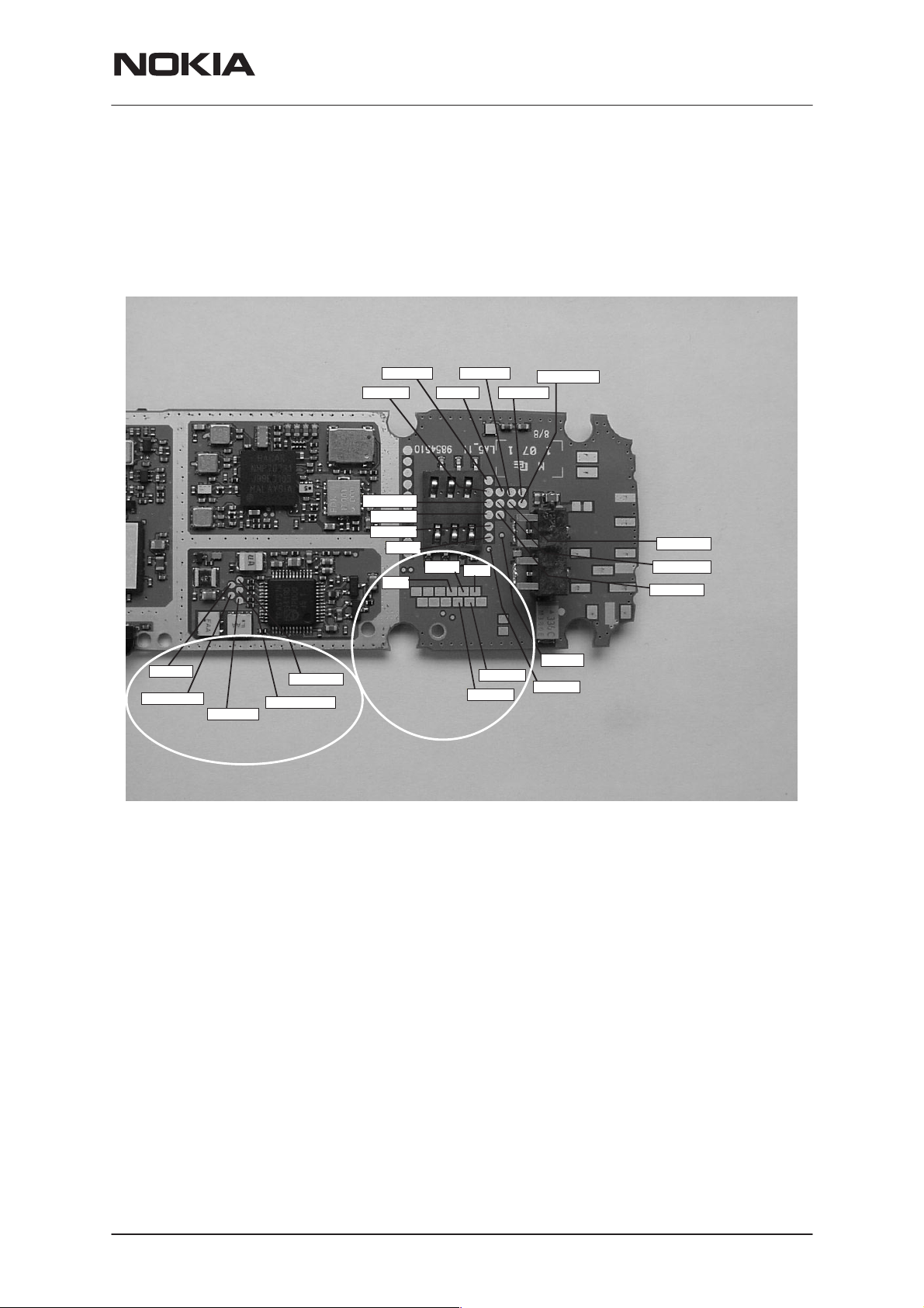
PWB Test Points
NPM–9
Troubleshooting Instructions
FMCLK
FMCTRLDA
FMWREN
FMCTRLCLK
FM RADIO
FMTUNEX
MBUSTX
FBUSRX
DBUSCLK
DBUSDA
UEMINT
PURX
GND
FBUSTX
MBUS
FPS–8
MBUSRX
VPP
FBUSTX
FBUSRX
SLEEPCLK
CBUSDA
CBUSCLK
DBUSENX1
CBUSENX
SLEEPX
EXTRDX
BLACK colored test points are connected to the lines between UEM and
UPP where the logic level is 1.8 V.
RED colored test points are connected to the lines from FPS–8 and have
2.7 V logic level.
BLUE test points are connected to FM radio lines and have 1.8 V logic
level.
Issue 1 02/2002
Nokia Corporation
Page 3
Page 4
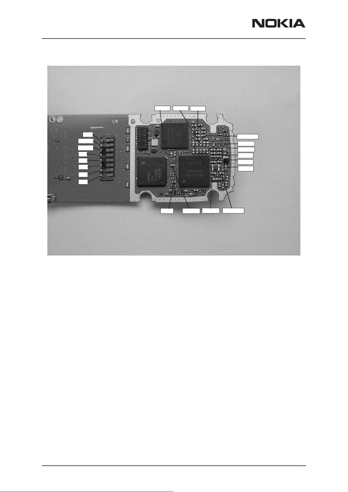
NPM–9
Troubleshooting Instructions
Measurement Points
PAMS Technical Documentation
VOUT
VDD 2.78 V
VDDI 1.8 V
SCLK
SDA
GND
XCS
XRES
Troubleshooting steps
VR5 2.78 V
VR7 2.78 V
VCORE 1.8VVIO 1.8V
VR3 2.78 V
VFLASH2 2.78 V
VR1B 4.75 V
VR1A 4.75 V
VR2 2.78 V
VR6 2.78 V
VR4 2.78 V
VANA 2.78 V VFLASH1 2.78 V
The following hints help to find the problem if the circuitry seems to be
faulty. The instructions are divided into following sections:
1. Phone is totally dead
2. Flash programming doesn’t work
3. Power doesn‘t stay on or the phone is jammed
4. Charging fault
5. Plug in SIM card is out of order (insert SIM card).
6. Audio fault
7. Display is not working
8. Keypad fault
The first thing to do is carry out a through visual check of the module. En-
sure in particular that:
a) there are not any mechanical damages
b) soldered joints are OK
Page 4
Nokia Corporation
Issue 1 02/2002
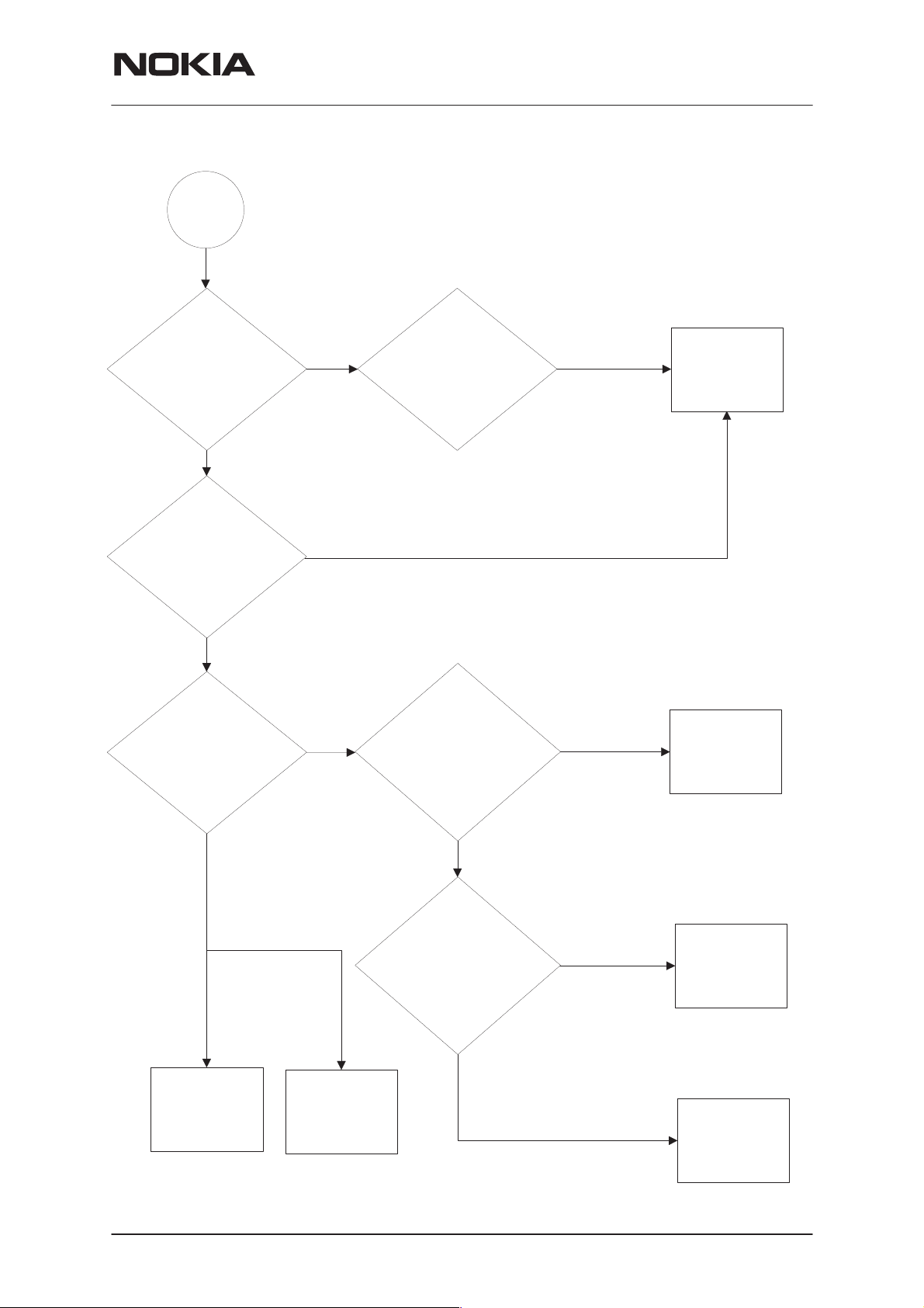
Page 5
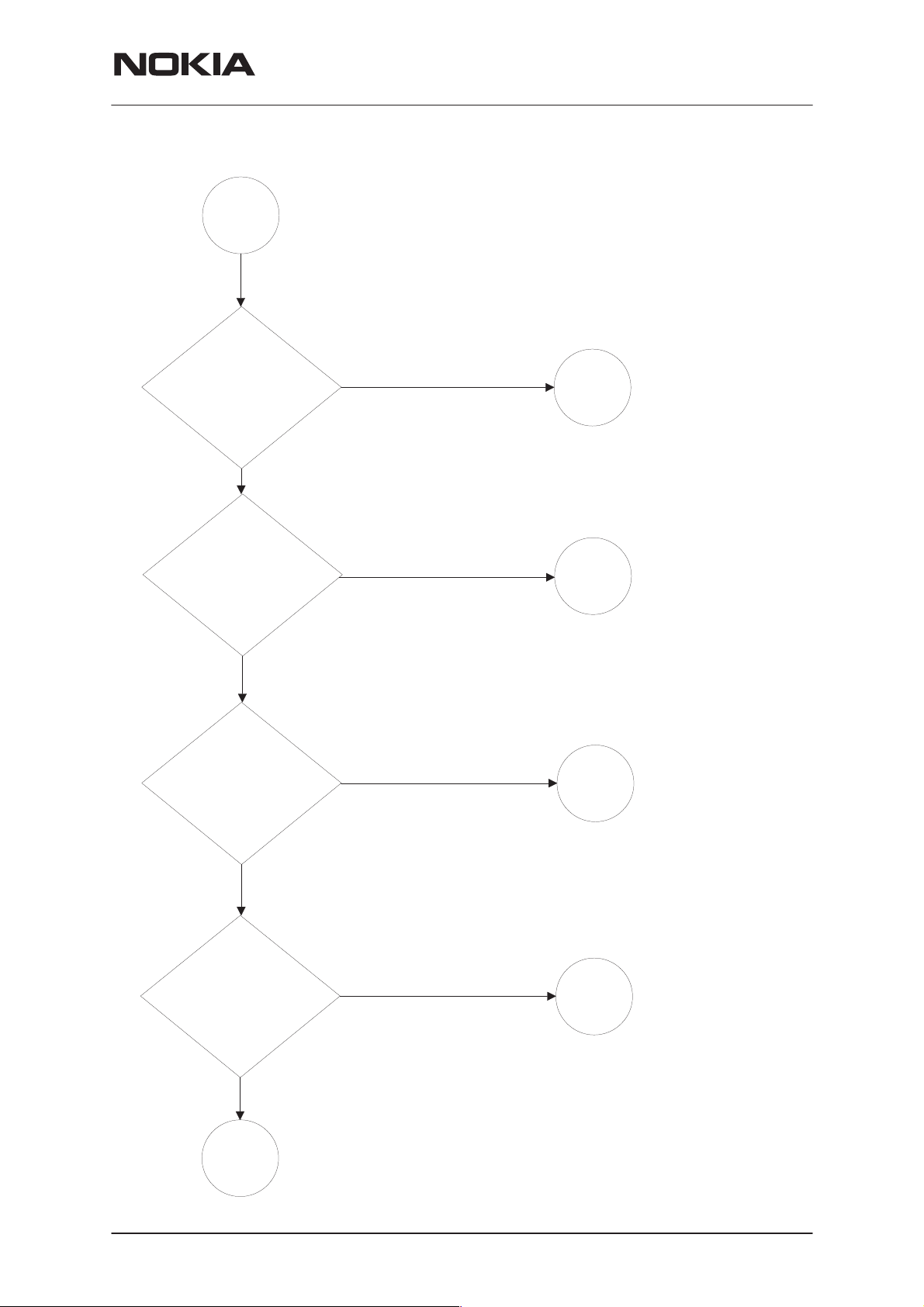
PAMS Technical Documentation
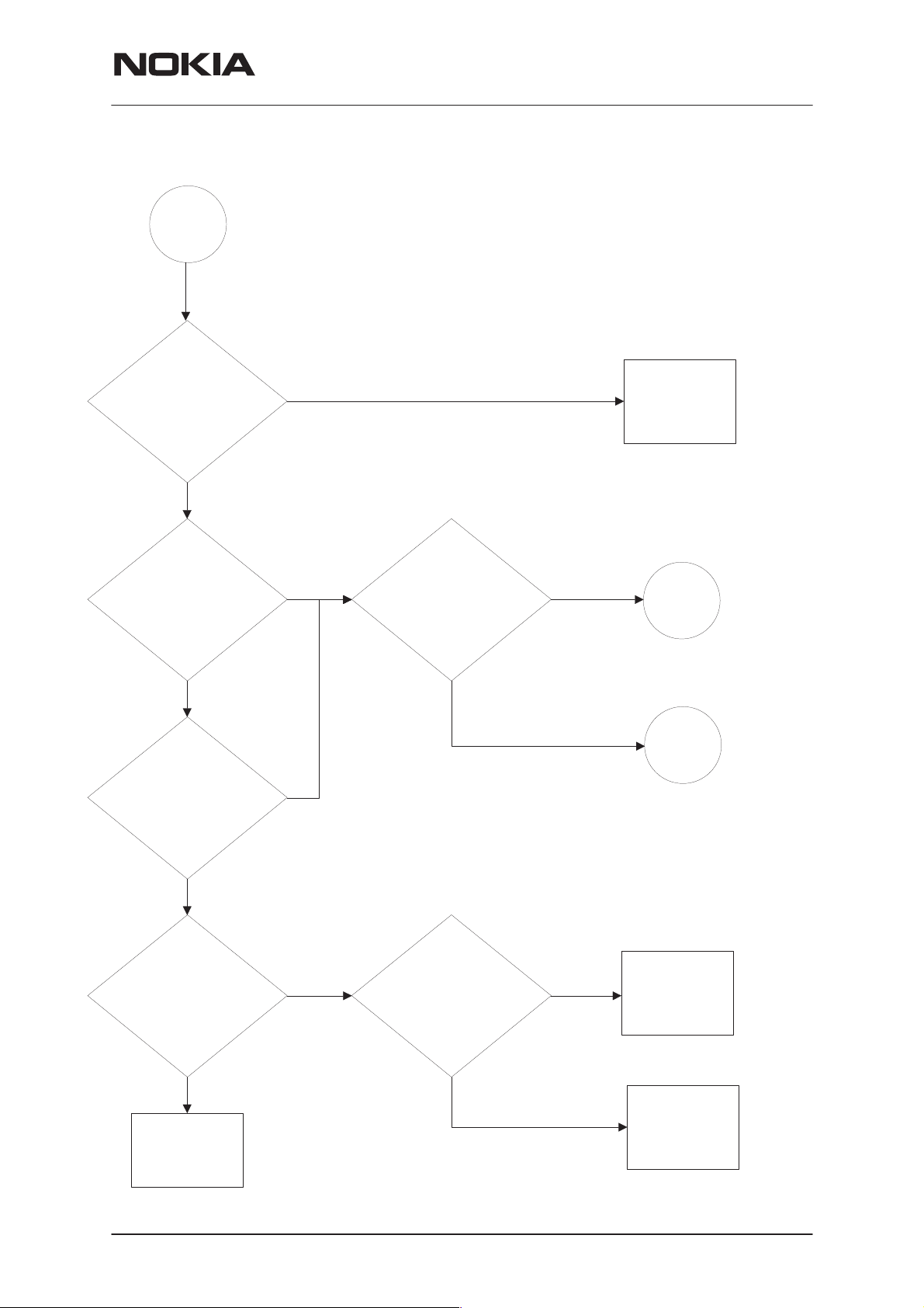
Main troubleshooting tree
TOP
NPM–9
Troubleshooting Instructions
Phone totally
dead
No
Flash programming
doesn’t work
No
Phone doesn’t
start up or the phone is
jammed
Yes
Yes
Yes
Phone is
dead
Flash
faults
Phone is
jammed
Charging
doesn’t work
TOP 2
Issue 1 02/2002
No
No
Yes
Nokia Corporation
Charger
Page 5
Page 6
NPM–9
Troubleshooting Instructions
TOP 2
PAMS Technical Documentation
Phone doesn’t read
SIM card
No
Audio faults
No
Display or LED’s
doesn’t work
Yes
Yes
Yes
SIM card
Audio
faults
Display
faults
Page 6
No
Keypad
doesn’t work
No
Yes
Nokia Corporation
Keypad
faults
END
Issue 1 02/2002
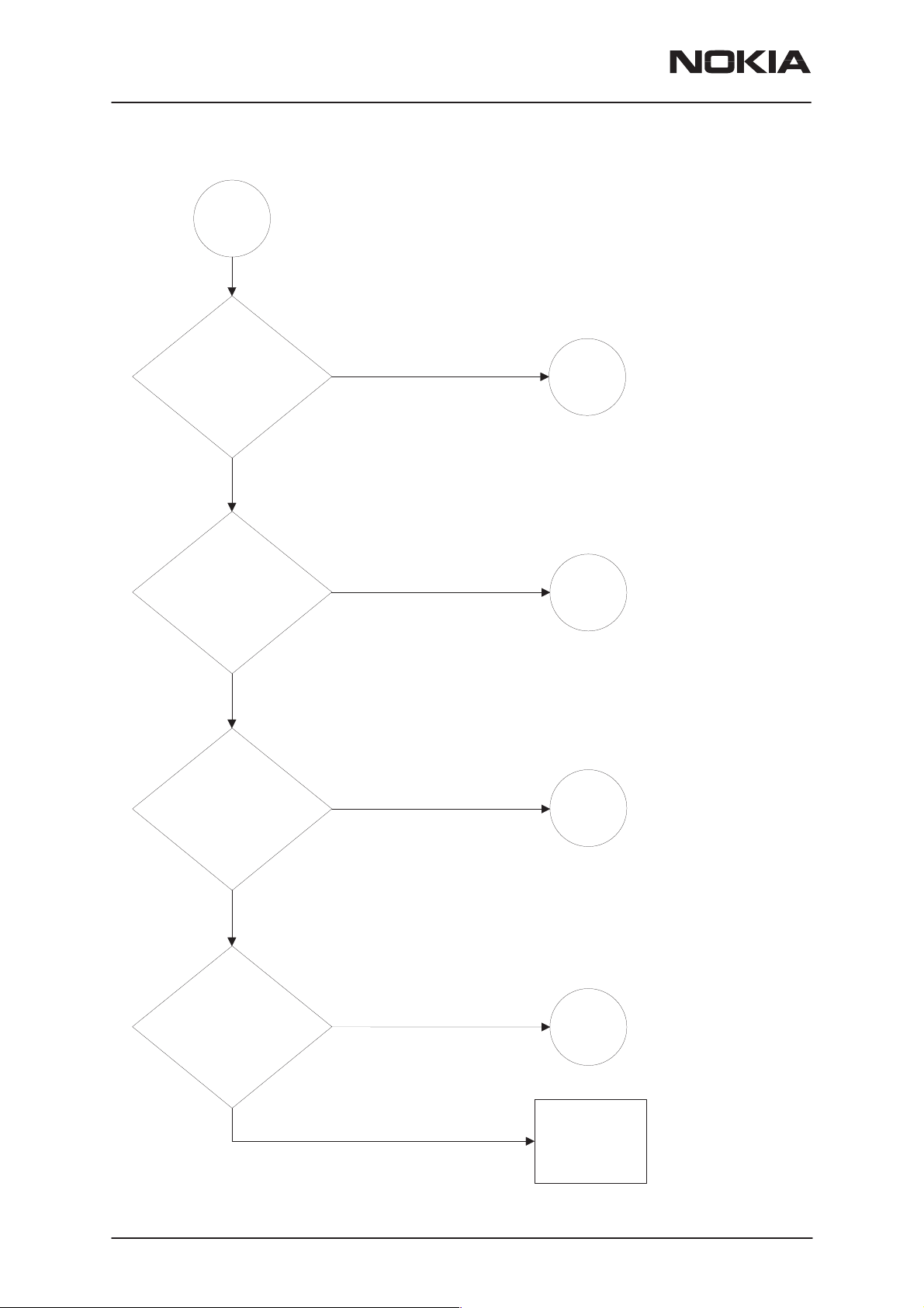
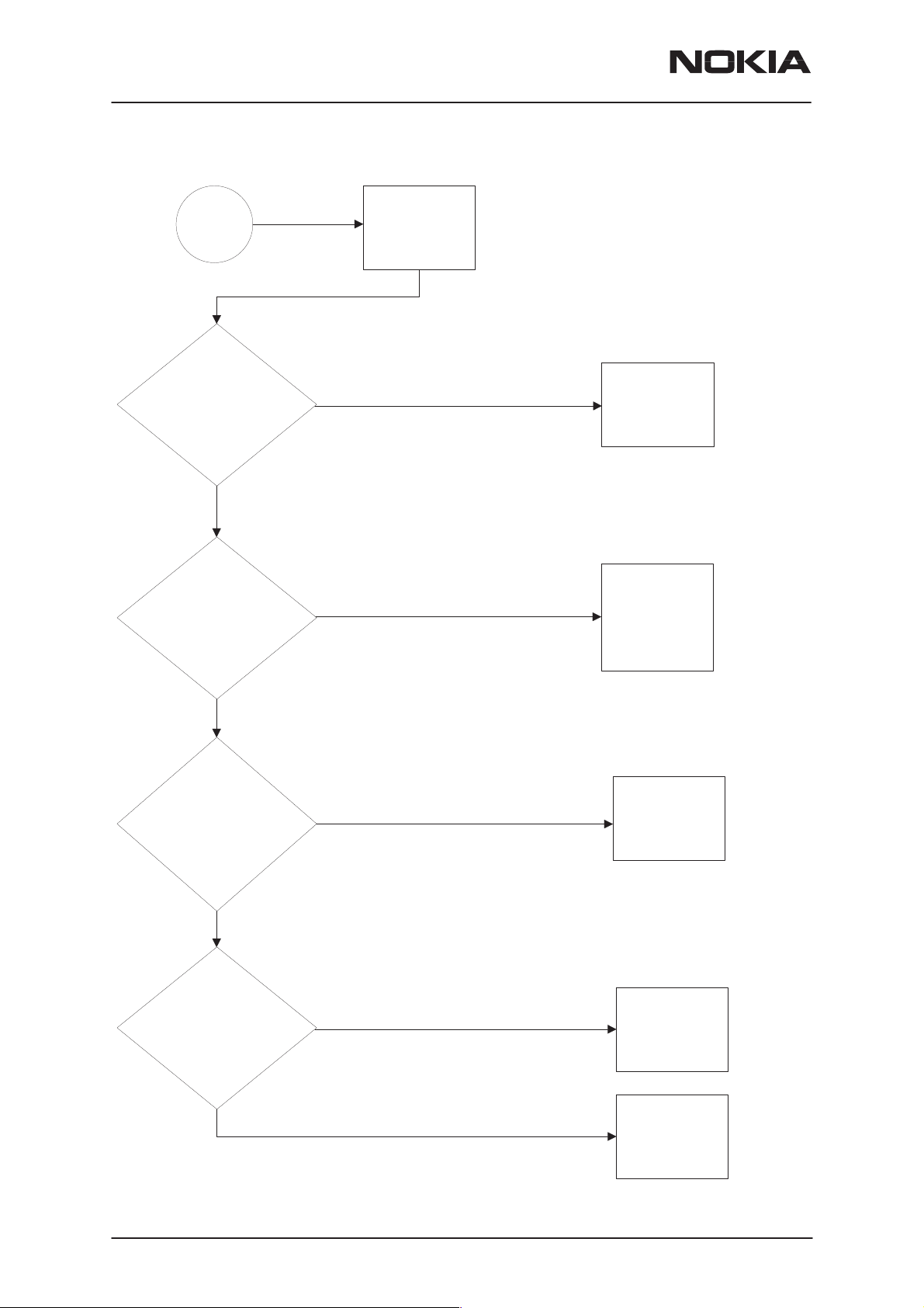
Page 7
PAMS Technical Documentation
Phone is dead
Phone is
dead
NPM–9
Troubleshooting Instructions
Phone current
is zero ?
No
Phone current is < 50mA
No
Phone current is ~ 54 mA
Yes
Yes
No
Is phone
flash programing OK ?
No
Yes
Check X101
solder and
VBATT lines
Phone is
jammed
Flash
faults
Yes
Is phone in LOCAL
MODE ?
Yes
OK retest
Issue 1 02/2002
No
Check BSI line
X101, C241, R203, C109,
Are they OK ?
Nokia Corporation
Yes
Change UEM
R202
No
Repair
Page 7
Page 8
NPM–9
Troubleshooting Instructions
Flash programming doesn’t work
Flash
faults
PAMS Technical Documentation
The Phone does
not set Flashbus TXD line
high after the startup.
No
Yes
Measure BSI pulse
during Flash
programming.
Is it OK ?
Yes
Measure FBUSTX
line during Flash
programming
from testpoint J411
Is it High (1.8V) ?
Yes
No
No
Check BSI line
X101, C241,
R203, C109,
R202
Check R102
If OK –>
Change UEM
Change UPP
The Phone does not set
Flashbus TXD line low after
the line has been high.
No
Flash faults
page 2
Page 8
Yes
Nokia Corporation
Change UPP
Issue 1 02/2002
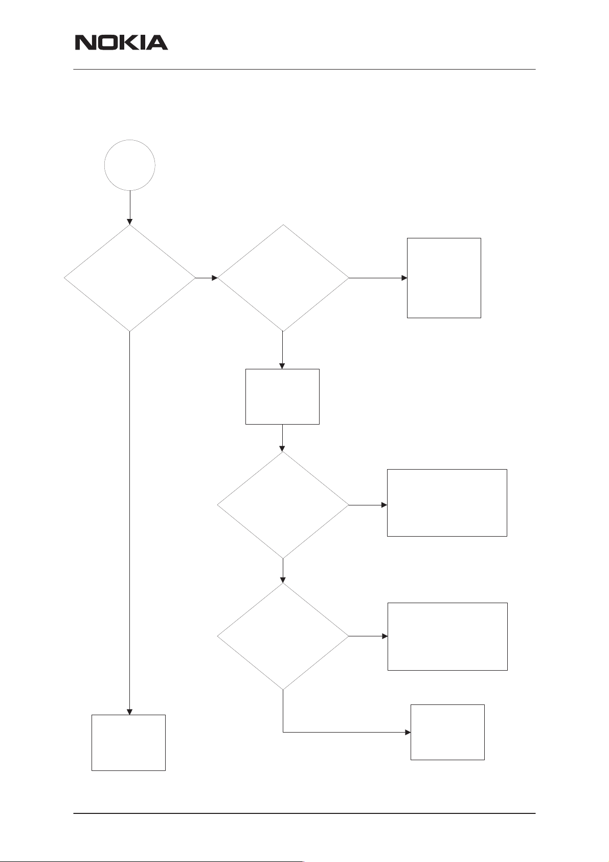
Page 9
PAMS Technical Documentation
Flash faults
page 2
NPM–9
Troubleshooting Instructions
Wrong manufactor ID
and Device ID
No
Is the phone totally dead ?
No
Phone
doesn’t start up
or the phone
is jammed ?
Yes
Yes
Yes
Change
FLASH
Phone is
dead
Phone is
jammed
Retest
Issue 1 02/2002
No
Nokia Corporation
Page 9
Page 10
NPM–9
Troubleshooting Instructions
Phone is jammed
Phone is
jammed
Measure
VIO, VCORE, FLASH1,
VANA, VR3 voltages.
Are they OK ?
Yes
No
Check VBATT1–6
VIO, VCORE,
FLASH1, VANA,
VR3 lines. Are
they OK?
Yes
PAMS Technical Documentation
Check
No
Z260 – Z265
C260 – C265
BSI / BTEMP
lines and
VBATT lines
Check BSI /
BTEMP lines. If
OK –>
UEM regulators
are not working
Change UEM
Measure
32.6kHz Sleep Clk
from testpoint J404
Is it OK ?
Yes
Measure
13MHz RFClk from R420.
Is it OK ?
Yes
No
No
Measure
32.6kHz Sleep Clk
from B200.
Is it OK ?
Yes
Measure 26MHz RFClk
from C660.
Is it OK ?
Yes
No
No
Check B200,
C209, C210
Change UEM
Check R661,
C661, R660,
C660 if OK
change G660
Check R420,
C420 if OK
change N600
Measure PURX
signal from testpoint J402
Is it high (1.8V)?
Yes
Jammed
Page 2
Page 10
No
Nokia Corporation
Change UEM
Issue 1 02/2002
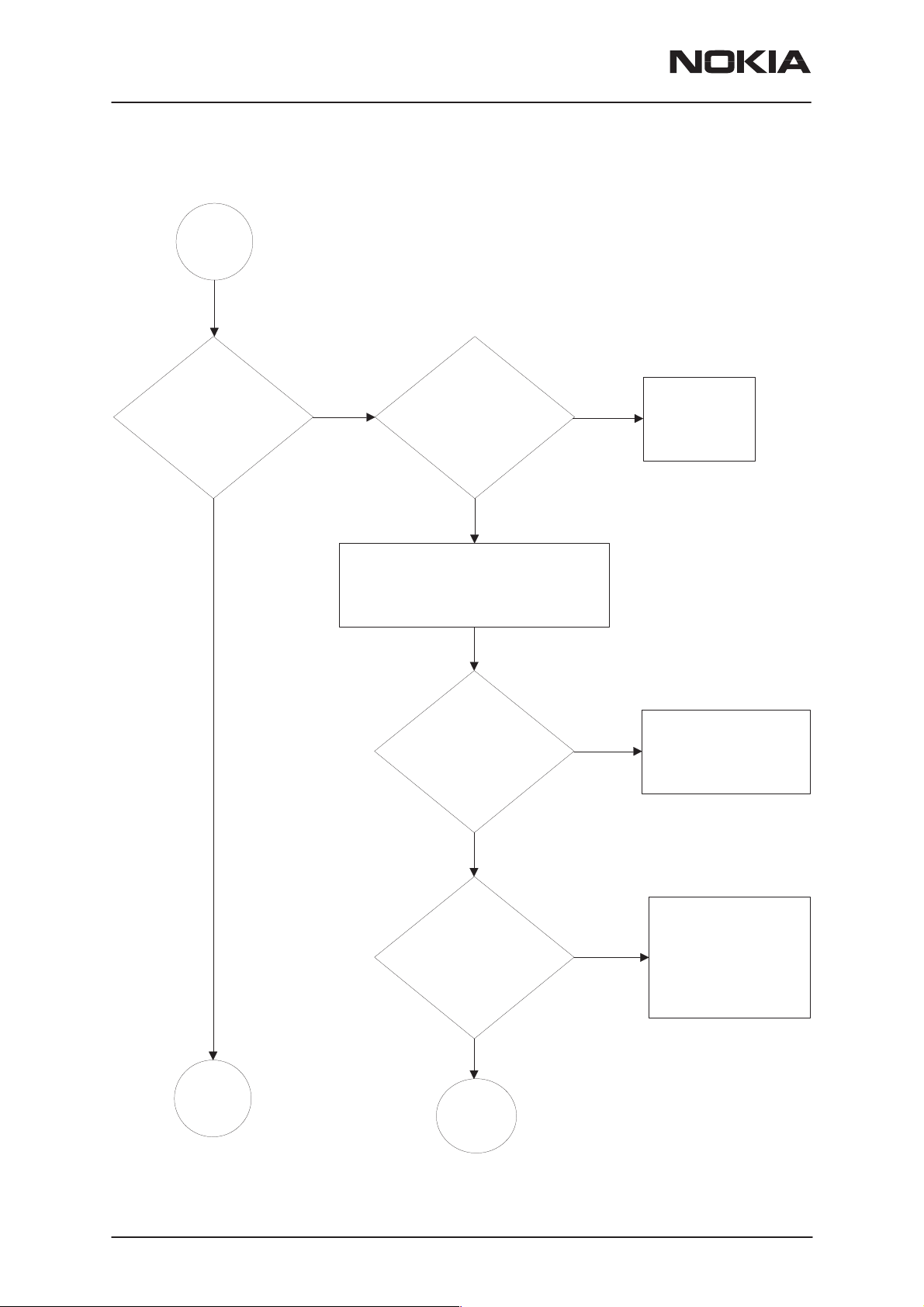
Page 11
PAMS Technical Documentation
Jammed
Page 2
NPM–9
Troubleshooting Instructions
Phone shutdown after
30s
No
Measure DBUSClk
1MHz signal
from testpoint J413
Is it OK ?
Yes
Read phone info.
Is it OK ?
Yes No
No
No
Measure watchdog
signal CBUSDA from
testpoint J414
Is it OK ?
Measure FBUSRX
signal during phone info read
from testpoint J412
Is it OK ?
Change UPP
No
Change UEM
Yes
Change LA5
module
Issue 1 02/2002
Yes
Measure FBUSTX
signal during phone info read
from testpoint J411
Is it OK ?
Yes
Retest
Nokia Corporation
No
Change UPP
Change UEM
Page 11
Page 12
NPM–9
Troubleshooting Instructions
Charging fault
PAMS Technical Documentation
Charger
Battery bar
doesn‘t work (scroll)
Yes
Measure voltage
over (TVS) V100.
Is it > 3.0 Vdc ?
No
No
Connect
(ACP–7)
charger
Retest
Check X100,
V100, C103,
C100, F100,
L100
and line
Yes
Read BTEMP value.
(Compare it to ambient
temperature)
Is it ~ 25 C (0319) ?
Yes
Remove (fuse) F100
and measure current.
Is it ~350...390 mA ?
Yes
No
No
Check
X101,C109
R202, C240,
R203 and line.
Change UEM
Retest
Page 12
Nokia Corporation
Issue 1 02/2002
Page 13
PAMS Technical Documentation
SIM card is out of order (insert SIM card)
SIM card
Insert SIM card
faults
Yes
Set phone LOCAL mode
Is it OK ?
Troubleshooting Instructions
Check BSI line
No
X101, C241,
R203, C109,
R202.
If OK –>
Change UEM
NPM–9
No
Yes
Check X386
Measure VSIM voltge
from X386
Is it 3V ?
Yes
Check SIM
power UP sequency
(Page 35 figure 19)
Is it OK ?
No
No
Check VSIM line,X386,
C203, C389.
If OK –> Change R388.
If still wrong VSIM
voltage –> Change UEM
Check SIM lines.
If OK –> Change R388.
If still fail –> Change UEM
END
Issue 1 02/2002
Yes
Nokia Corporation
Change UPP
Page 13
Page 14
NPM–9
Troubleshooting Instructions
Audio fault
Audio
faults
PAMS Technical Documentation
Is earpiece working?
Yes
No
Try change earpiece.
Is it working now ?
No
Set phone in LOCAL mode.
Use Phoenix Audio Test.
Set EXT IN, HP OUT, LOOP ON.
Measure DC
offset voltage
from Earpiece pads.
Is it ~1.38V ?
Yes
Yes
No
Retest
Check L151, C160,
R164 and line.
If OK
–> Change UEM
Page 14
Audio
faults 2
Measure MICB2
voltage from XMICP pads
(L106) .
Is it ~2.2V ?
Earpiece
2
Nokia Corporation
Yes
No
Check L106, C112,
R161, C163, R166,
C165, R167 and
line.
If OK
–> Change UEM
Issue 1 02/2002
Page 15

PAMS Technical Documentation
Earpiece
2
Connect EXT audio signal 1kHz
(sine) (¨200mVp–p) in XMICP pads
and Ground in XMICN
NPM–9
Troubleshooting Instructions
Measure sine signal
from earpiece pads.
Is it ~880mVp–p ?
Yes
Retest
No
Measure sine signal
from UEM (R156)
Is it ~130mVp–p ?
No
Yes
Change UEM.
Check R156, C153,
C155, R166, R167,
C163, R161 and
line.
Issue 1 02/2002
Nokia Corporation
Page 15
Page 16

NPM–9
Troubleshooting Instructions
Audio
faults 2
PAMS Technical Documentation
Is microphone working?
Yes
No
Try change bottom
connector X100.
Is it working now ?
No
Set phone in LOCAL mode.
Use Phoenix Audio Test.
Set HP IN, EXT OUT, LOOP ON.
Measure MICB1
voltage from MICP pads.
Is it ~2.1V ?
Yes
No
Retest
Check L105,
C105, C152,
C156, R152,
C168, C166,
C215 and line.
If OK –>
Change UEM
Page 16
Audio
faults 3
Check C151,
R157, C105,
C154 and line.
If OK –>
Change UEM
Nokia Corporation
Yes
Issue 1 02/2002
Page 17

PAMS Technical Documentation
Audio
faults 3
NPM–9
Troubleshooting Instructions
Is BUZZER working?
Yes
No
Measure VBATT
voltage from B301.
Is it OK?
Yes
Set phone in LOCAL mode.
Use Phoenix Audio Test.
Set Buzzer volume ON.
Measure Buzzer
control signal
from BUZZER (C307).
Is it 1kHz pulses ?
No
Yes
Check VBATT
line
Change
BUZZER
(B301)
END
Issue 1 02/2002
No
Check C306,
C307, C308
and line.
IF OK –>
Change UEM
Nokia Corporation
Page 17
Page 18

NPM–9
Troubleshooting Instructions
Display fault
Display
faults
Set phone into local mode.
Start Display test with Phenix
PAMS Technical Documentation
Try change UI module
Is it working now ?
Yes
Retest
Are the UI–module
led’s turned on ?
Yes
No
Measure signal
from X303 pin. 2.
Is it 128 Hz
~3.3Vp–p ?
No
Check R306 If OK.
Measure VBATT
from V300 pin. 4
Is it OK?
No
Check X303
Yes
No
Check X303
Check R304
and VBATT
line
Page 18
Display
faults 2
Yes
Measure
PWM LED‘s
control signal from UEM
Is it 128 Hz
~3.8Vp–p ?
Yes
Nokia Corporation
Check control
signal line if OK
Change UEM
No
Check R305,
V300, V329
and line
Issue 1 02/2002
Page 19

PAMS Technical Documentation
Display
faults 2
NPM–9
Troubleshooting Instructions
Are the display
led’s turned on ?
Yes
No
Measure signal
fromV301 pin. 3.
Is it 128 Hz
~3.3Vp–p ?
No
Measure VBATT
from V301 pin. 4
It is OK?
Yes
Measure
PWM LED‘s
control signal from UEM
Is it 128 Hz
~3.8Vp–p ?
Yes
No
No
Check LED‘s
and line
Check R307
and VBATT
line
Check control
signal line.
If OK,
Change UEM
Check R305,
V301, V329
and line
Display
faults 3
Issue 1 02/2002
Yes
Nokia Corporation
Page 19
Page 20

NPM–9
Troubleshooting Instructions
Display
faults 3
PAMS Technical Documentation
Does the display start ?
Yes
VDD (2.78V) and
No
Measure
VDDI (1.8V).
Is it OK?
Yes
Try change UI module
Is it working now ?
No
Check X300
No
Yes
Retest
Check C303
and lines.
If OK,
Change UEM
Measure
VOUT voltage.
Is it ~8.1V?
Yes
Measure
XRES, XCS.
Is it ~1.8 V?
Yes
END
No
No
Check C302,
X300 and lines.
Check X300
and lines.
If OK, change
UPP
Page 20
Nokia Corporation
Issue 1 02/2002
Page 21

PAMS Technical Documentation
Keypad fault
Keypad
faults
No
Is the power key working ?
Measure voltage
from S300
Is it HIGH ?
Troubleshooting Instructions
Check R301,
No
C312, S300
and line.
If OK –>
Change UEM
NPM–9
Yes
Measure voltage
from S300 when
power key is pressed.
Is it HIGH ?
No
Yes
Yes
Chech S300.
Is it OK ?
No
Yes
Phone is
dead
Change S300
Phone is
jammed
Keypad
faults 2
Issue 1 02/2002
Nokia Corporation
Page 21
Page 22

NPM–9
Troubleshooting Instructions
Keypad
faults 2
PAMS Technical Documentation
No
Is UI module keys working ?
Yes
Try change UI module.
Is it working now ?
No
Check X303
Measure ROW0,
ROW1, ROW2, ROW3,
ROW4 lines from X303.
Are they ~1.8V ?
Yes
Yes
No
Retest
Check ROW0 –
4 Lines, X303.
If OK change
Z301. If still fail
change UPP
Keypad
faults 3
Measure SLEEPX
signal from J403
when key is pressed.
Is it ~1.8V?
Yes
When keypad
is pressed, the led’s are
turned on ?
Yes
No
No
Check ROW0 –
4 Lines, X303.
If OK change
Z301. If still fail
change UPP
Check ROW0 –
4 Lines, X303.
If OK change
Z301. If still fail
change UPP
Display
faults
Page 22
Nokia Corporation
Issue 1 02/2002
Page 23

PAMS Technical Documentation
Keypad
faults 3
No No
Is volume UP key working ?
Measure ROW0
line from S301.
Is it ~1.8 V ?
NPM–9
Troubleshooting Instructions
Check S301,
S302, lines.
If OK change
Z301.
If still FAIL
change UPP
Yes
Is volume DOWN key
working ?
Yes
END
No
Measure COL1
from S301 when
S301 is pressed
Is there
50us pulse ?
Measure ROW0
line from S302.
Is it ~1.8 V ?
Yes
Measure COL4
from S302 when
S302 is pressed
Is there
50us pulse ?
Yes
Yes
No
No
No
Check S301,
S302, lines.
If OK change
change UPP
and COL1 line.
If OK change
Change UPP
Z301.
If still FAIL
Change UPP
Check S301
Z301.
If still FAIL
change UPP
Check S302
and COL4 line.
If OK change
Z301.
If still FAIL
change UPP
Issue 1 02/2002
Yes
Nokia Corporation
Page 23
Page 24

NPM–9
Troubleshooting Instructions
RF Troubleshooting
Introduction
Measurements should be done using spectrum analyzer with high–frequency high–impedance passive probe (LO–/reference frequencies and
RF power levels) and oscilloscope with a 10:1 probe (DC–voltages and
low frequency signals).
The RF–section is build around one RF–ASIC (HAGAR N600). Before
changing HAGAR, please check following things: Supply voltages are OK
and serial communication coming from baseband to HAGAR.
Please note: Grounding of the PA module is directly below PA module
making it difficult to check or change. Most RF semiconductors are
static discharge sensitive! So ESD protection must be taken care of
during repair (ground straps and ESD soldering irons). HAGAR and PA
are moisture sensitive and must be pre–baked prior to soldering.
PAMS Technical Documentation
Troubleshooting discrete components (resistors, inductors and capacitors) is done by checking component soldering. Capacitors can be
checked for shortening and resistor values using an ohmmeter, but remember in–circuit measurements are evaluated with caution.
Remember that all measured voltages or RF levels in this document are
rough figures. Especially RF levels vary due to different measuring equipment or different probe grounding used . When using RF probe it is good
to use metallic tweezers to connect probe ground to PWB ground as
close to measurement point as possible.
Page 24
Nokia Corporation
Issue 1 02/2002
Page 25

PAMS Technical Documentation
RF Key Components
NPM–9
Troubleshooting Instructions
EGSM LNA
GSM1800 LNA
Dual RX SAW
Dual coupler
Antenna switch
Antenna pad
Dual PA
EGSM TX SAW
GSM1800 TX balun
GSM1800 RX 2nd SAW
EGSM RX 2nd SAW
FM IF filter 2
FM IF filter 1
Hagar RFIC
VCO balun
FM receiver IC
FM diskriminator
26MHz XO
4GHz VCO
Issue 1 02/2002
Nokia Corporation
Page 25
Page 26

NPM–9
Troubleshooting Instructions
PWB Test Points
PAMS Technical Documentation
1800 1st SAW out
900_RX
900 antsw tx contr
1800 antsw contr
1800_RX
1800
PA ctrl
Antenna
pad
900
PA ctrl
900 PA
bias
1800 PA bias
900 PA in
900 1st SAW out
LNA_P
LNAB_P
LNA_G
900 Mod out
1800 Mod out
1800 PA in
1800 LNA out
LNAB_G
VR2
900 LNA out
VrefRf01
VR4 VR6
FMdiscr .
IF out 1
IF out 2
VrefRf02
VR5
RX_Q
13M clock
RX_I
26M xo out
AFC
SLE
SCLK
VR3
4G VCO out
SDATA
VR7
4G VCO ctrl
TX_I_0
FM audio
Vtune
TX_Q_0
VR1a
LCtank1
LCtank2
Page 26
Nokia Corporation
Issue 1 02/2002
Page 27

PAMS Technical Documentation
Transmitter
General instructions
Connect test jig to computer with DAU9S cable or to FPS–8 Flash Prommer with XCS–4 modular cable.
Make sure that you have PKD–1 dongle connected to computers parallel
port.
Connect DC power supply to module test jig with FLC–2 cable.
NOTE: When repairing or tuning transmitter use external DC supply with
at least 3A current capability. Set the DC supply voltage to 3.9V and set
the jumper connector on test jig to ”bypass” position.
Connect RF–cable to the module test jig (MJS–46) RF connector and to
measurement equipment or at least 10dB attenuator, otherwise the PA
may be damaged. Normally spectrum analyzer is used as measurement
equipment.
NOTE: Normally Spectrum analyzer maximum input power is +30dBm. It
is recommended to use 10dB attenuator on Spectrum analyzer input to
prevent damage.
NPM–9
Troubleshooting Instructions
Set the phone module to test jig and start Phoenix service sofware.
Initialize connection to phone. (use FBUS driver when using DAU9S and
COMBOX driver when using FPS–8)
Select product from the menu: File –> Choose product –> NPM–9
From toolbar set operating mode to ”Local”.
Activate RF controls window from the menu:
Maintenance –> Tuning –> RF Controls
From the RF controls window:
– Select band ”GSM900” or ”GSM 1800” (Default = ”GSM900”)
– Set Active unit to ”Tx” (Default = ”Rx”)
– Set Operation mode to ”Burst” (Default = ”Burst”)
– Set Tx data type to ”Random” (Default = ”All1”)
– Set Rx/Tx channel to 37 on GSM900 band or 700 on GSM1800 band
(Defaults)
– Set Tx PA mode to ”Free” (Default)
– Set power level to 5 (Default = 19) on GSM900 or to 0 (Default = 15)
on GSM1800
Issue 1 02/2002
Nokia Corporation
Page 27
Page 28

NPM–9
Troubleshooting Instructions
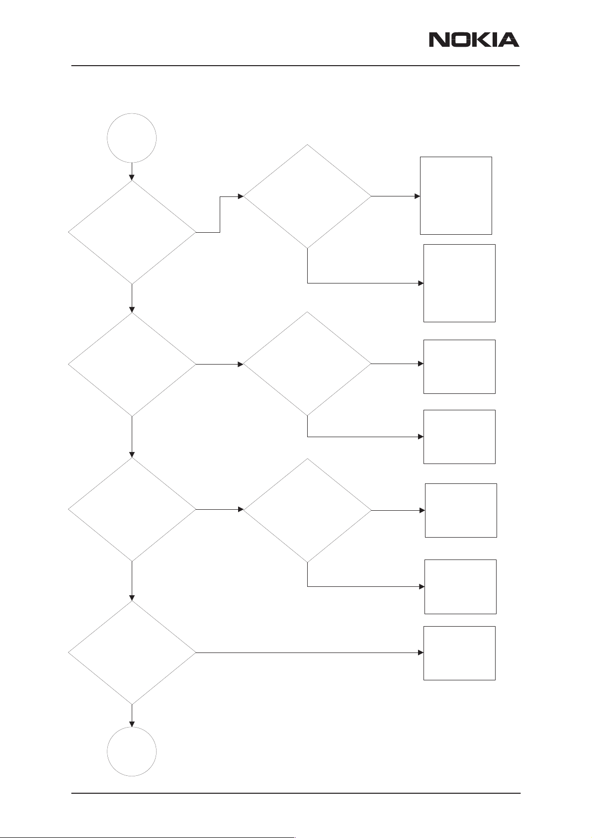
Transmitter troubleshooting diagram
PAMS Technical Documentation
Page 28
Nokia Corporation
Issue 1 02/2002
Page 29

PAMS Technical Documentation
NPM–9
Troubleshooting Instructions
Issue 1 02/2002
Nokia Corporation
Page 29
Page 30

NPM–9
Troubleshooting Instructions
PAMS Technical Documentation
Page 30
Nokia Corporation
Issue 1 02/2002
Page 31

PAMS Technical Documentation
Transmitter signals
NPM–9
Troubleshooting Instructions
TX_I_0, Tx on, Random data, Burst mode
900/1800 antsw tx contr, Tx on, Burst mode
TX_Q_0, Tx on, Random data, Burst mode
900/1800 PA bias, Tx on, Burst mode 900/1800 PA ctrl, Tx on, Burst mode, High
power level
Issue 1 02/2002
Nokia Corporation
Page 31
Page 32

NPM–9
Troubleshooting Instructions
PAMS Technical Documentation
GS MPOW Tue Sep 25 13: 48: 59 2001
REF41.0dBm ATT40dB
10dB/
REF OFS
11. 0 dB
RBW
100 kHz
VBW
100 kHz
SWP
2. 0 s
CENTER 897 . 400 MHz SPAN 2 . 000 MHz
A_ wr i t eB_bl ank
Tx out signal, 900 band, burst mode, channel 37
Page 32
Nokia Corporation
Issue 1 02/2002
Page 33
PAMS Technical Documentation
Receiver
General instructions
Connect test jig to computer with DAU9S cable or to FPS–8 Flash Prommer with XCS–4 modular cable. Make sure that you have PKD–1 dongle
connected to computers parallel port.
Connect DC power supply to module test jig with FLC–2 cable. Set the
DC supply voltage to 3.9V and set the jumper connector on test jig to
”bypass” position.
Connect RF–cable to the module test jig (MJS–46) RF connector and to
RF signal generator.
Set the phone module to test jig and start Phoenix service sofware.
Initialize connection to phone. Use FBUS driver when using DAU9S and
COMBOX driver when using FPS–8.
Choose product from the menu: File –> Choose product –> NPM–9.
NPM–9
Troubleshooting Instructions
From toolbar set operating mode to ”Local”.
Activate RF controls window from the menu: Maintenance –> Testing –>
RF Controls.
From the RF controls window:
– Select band ”GSM900” or ”GSM 1800” (Default = ”GSM900”)
– Set Active unit to ”Rx” (Default = ”Rx”)– Set Operation mode to
”Continuous” (Default = ”Burst”)
– Set AGC to ”8: FEG ON + 46 dB (Default = ”8: FEG ON + 46 dB”)
– Set Rx/Tx channel to 37 on GSM900 band or 700 on GSM1800 band
(Defaults)
Apply 942.46771 MHz (channel 37 + 67.710 kHz offset) or 1842.86771
MHz (channel 700 + 67.710 kHz offset) –90 dBm signal to the RF–connector (remember to compensate for cable attenuation).
Measuring with an oscilloscope on ”RX_I” or ”RX_Q” this picture should
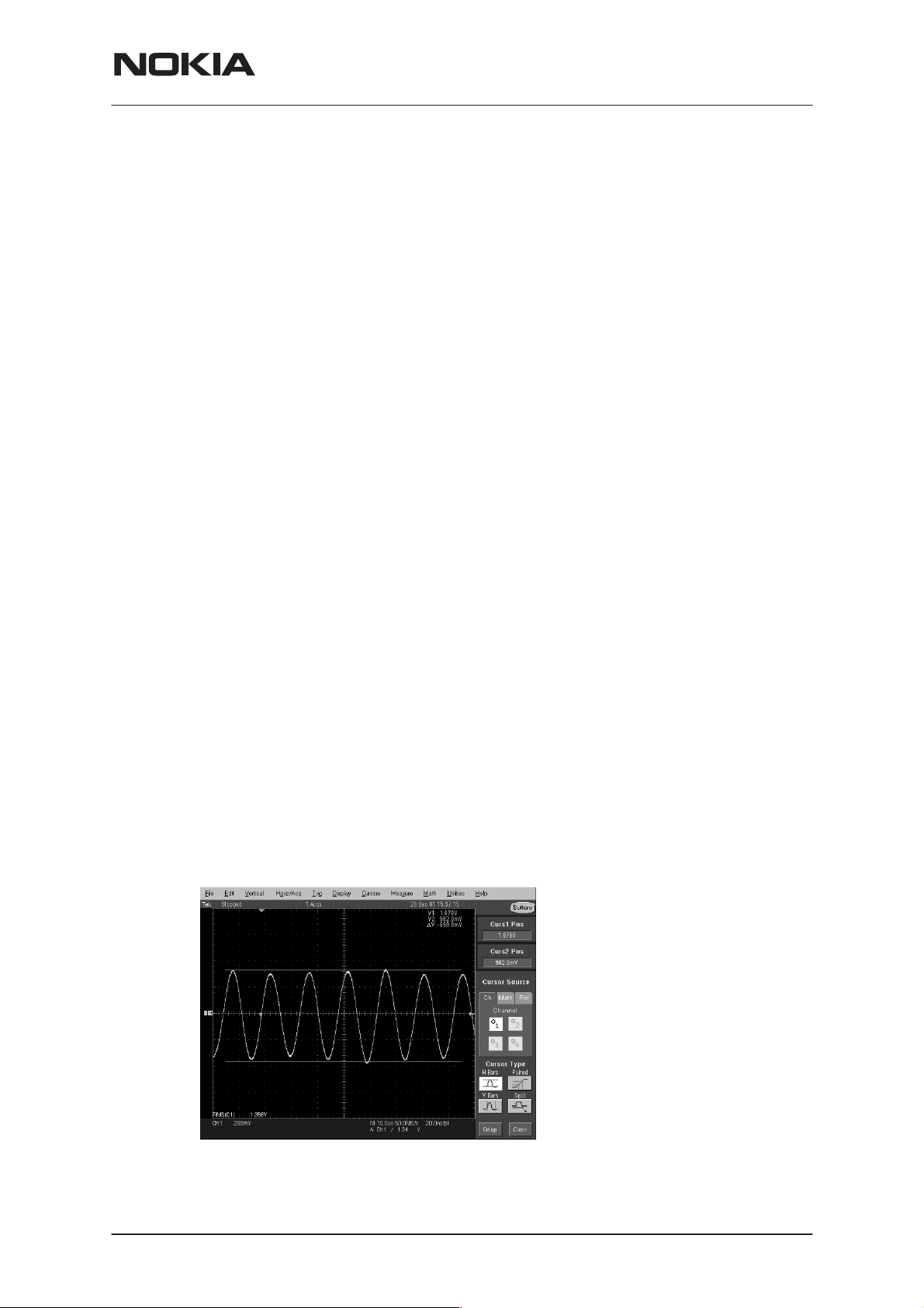
be seen on a working GSM900 or GSM1800 receiver:
Signal amplitude is 700 mVpp, DC offset 1.35 V and frequency 67 kHz. If
this picture is not seen, continue to the next page.
Issue 1 02/2002
Nokia Corporation
Page 33
Page 34

NPM–9
Troubleshooting Instructions
PAMS Technical Documentation
Receiver troubleshooting diagram for GSM900
Apply –90dBm
942.46771MHz signal
from generator to antenna connector
Yes
Oscilloscope at RX_I
Signal 700mVpp
DC offset 1.35V Frequency 67.7kHz
Yes
EGSM RX chain functional
No
Change generator level
to –50dBm
Spectrumanalyzer
900 LNA out
–61 dBm
Yes
NoYes
Spectrumanalyzer
900 1st SAW out
–80 dBm
Oscilloscope
LNA_G 2.7V
LNAB_G 2.7V
Spectrumanalyzer
V500, RFout –57
dBm
Oscilloscope
V500, RFout 2.7V
V500, RFin 0.8 V
Yes
Yes
Spectrumanalyzer
900_RX
–79 dBm
Check dual RX SAW
Z520
Oscilloscope
VR4 2.7V
Check Hagar serial interface Check
R501
Check Hagar
N600
Yes
Check C502
NoNo
Check V500,
L500, R502
Yes
Yes
NoNo
NoNo
Check Antenna switch
Z500
Check Baseband
Spectrumanalyzer
900 bal out
–66 dBm
Yes
Oscilloscope
VR4 2.7V
Check Hagar serial
interface (burst mode)
Yes
Spectrumanalyzer
4G VCO out
3769.6MHz
∼–30 dBm (*
Yes
Check Hagar N600
Check V500, C501,
L502, L503
No
Check Z501, C505,
C506, L501
No
Check Baseband
No
Synthesizer troubleshooting
Yes
All spectrumanalyzer reading
values are measured with 1
kohm passive probe (use
tweezers to connect the
probe ground to the nearest
PWB ground). Reading value
is represented without +26
dB compensation.
* Spectrumanalyzer
reading with 1 kohm
passive probe (right value add +26 dB)
Page 34
Nokia Corporation
Issue 1 02/2002
Page 35

PAMS Technical Documentation
Troubleshooting Instructions
Receiver troubleshooting diagram for GSM1800
Apply –90dBm
1842.86771MHz signal
from generator to antenna connector
Oscilloscope at RX_I
Signal 700mVpp
DC offset 1.35V Frequency 67.7kHz
Change generator level
to –50dBm
Spectrumanalyzer
1800 LNA out
–61 dBm
Spectrumanalyzer
1800 1st SAW out
–77 dBm
Spectrumanalyzer
1800_RX
–78 dBm
NPM–9
NoNoNoYesNoYes
Check Antenna switch
Z500
Yes
GSM1800 RX chain
functional
Yes
Yes
Oscilloscope
LNA_P 0V
LNAB_P 2.7V
Yes
Spectrumanalyzer
V550,
RFout –58 dBm
Oscilloscope
V550, RFout 2.6V
V550, RFin 0.8 V
Yes
Check V550, C551,
L552
Check dual RX SAW
Z520
Oscilloscope
VR4 2.7V
Check Hagar serial interface (burst
mode)
Check Hagar
N600
Yes
Check C552
NoNo
Check V550,
R551, L550,
R558
Yes
Yes
NoNo
Check Baseband
Issue 1 02/2002
No
Spectrumanalyzer
1800 bal out
–66 dBm
Oscilloscope
VR4 2.7V
Check Hagar serial
interface (burst mode)
Spectrumanalyzer
4G VCO out
3685.6MHz
∼–30 dBm (*
Yes
Check Hagar N600
Check Z551, C555,
C556, L551
NoYes
Check Baseband
NoYes
Synthesizer troubleshooting
Nokia Corporation
All spectrumanalyzer reading
values are measured with 1
kohm passive probe (use
tweezers to connect the
probe ground to the nearest
PWB ground). Reading value
is represented without +26
dB compensation.
* Spectrumanalyzer
reading with 1 kohm
passive probe (right value add +26 dB)
Page 35
Page 36

NPM–9
Troubleshooting Instructions
PAMS Technical Documentation
LNA gainstep checking GSM900 & GSM1800
900 LNA out 1800 LNA out
– RF–level at antenna port eg. –50 dBm
– RX continuous mode (local mode)
– difference between AGC –settings
”FEG on” and ”FEG off”
roughly 25 dB (using 250 ohm
passive RF–probe)
LNAB_G LNAB_P
– RX continuous mode (local mode)
– 2,6 V DC voltage ”FEG ON”
– 0 V DC voltage ”FEG OFF”
LNA_G 1800 LNA_P
– RX continuous mode (local mode)
– 2,7 V DC voltage ”FEG ON” and ”FEG
OFF”
– RF–level at antenna port eg. –50 dBm
– RX continuous mode (local mode)
– difference between AGC –settings
”FEG on” and ”FEG off”
roughly 30 dB (using 250 ohm passive
RF–probe)
– RX continuous mode (local mode)
– 2,7 V DC voltage ”FEG ON”
– 0 V DC voltage ”FEG OFF”
– RX continuous mode (local mode)
– 0 V DC voltage ”FEG ON”
– 1.9 V DC voltage ”FEG OFF”
Page 36
Nokia Corporation
Issue 1 02/2002
Page 37

PAMS Technical Documentation
Synthesizer
General instructions
Connect test jig to computer with DAU–9S cable or to FPS–8 Flash Prommer with XCS–4 modular cable.
Make sure that you have PKD–1 dongle connected to computers parallel
port.
Connect DC power supply or FPS–8 to module test jig with FLC–2 cable.
Set the DC supply voltage to 3.9V and set the jumper connector on test
jig to ”bypass” position.
Set the phone module to test jig and start Phoenix service sofware.
Initialize connection to phone. (use FBUS driver when using DAU–9S and
COMBOX driver when using FPS–8)
Select product from the menu: File –> Choose product –>NPM–9
From toolbar set operating mode to ”Local”.
NPM–9
Troubleshooting Instructions
Activate RF controls window from the menu:
Maintenance –> Tuning –> RF Controls
From the RF controls window:
– Select band ”GSM900” or ”GSM 1800” (Default = ”GSM900”)
– Set Active unit to ”Rx” (Default = ”Rx”)
– Set Operation mode to ”Continuous” (Default = ”Burst”)
– Set Rx/Tx channel to 37 on GSM900 band or 700 on GSM1800 band
(Defaults)
Issue 1 02/2002
Nokia Corporation
Page 37
Page 38

NPM–9
Troubleshooting Instructions
Synthesizer troubleshooting diagram
PAMS Technical Documentation
Page 38
Nokia Corporation
Issue 1 02/2002
Page 39

PAMS Technical Documentation
Synthesizer signals
NPM–9
Troubleshooting Instructions
26MHz XO out
4GHz VCO ctrl
900 RX, channel 124, continuous mode
13MHz clock
4GHz VCO ctrl
1800 TX, channel 512, continuous mode
Issue 1 02/2002
Nokia Corporation
Page 39
Page 40

NPM–9
Troubleshooting Instructions
PAMS Technical Documentation
REF –20 . 0 dBm ATT 10 d B
Fr i May 11 13: 03: 26 2001
10dB/
MK R
3. 610400 GHz
RBW
10 kHz
VBW
10 kHz
SWP
50 ms
CENTER 3. 6104000 GHz SPAN 2. 00 0 MHz
A_ v i ewB_bl ank
MARKER
3. 610400 GHz
–30. 72 dBm
4GHz VCO output, 1800 band, RX on, continuous mode
Page 40
Nokia Corporation
Issue 1 02/2002
Page 41

PAMS Technical Documentation
FM Radio troubleshooting
NPM–9
Troubleshooting Instructions
FM Radio component layout
Components L101, C101 and C102 are not shown in picture. Compo-
nents are placed in baseband section.
Issue 1 02/2002
Nokia Corporation
Page 41
Page 42

NPM–9
Troubleshooting Instructions
FM Radio troubleshooting diagram
PAMS Technical Documentation
Note 1. RF test signal parameters:
A,
– Amplitude,
– Carrier ferquency,
– Deviation, ∆
– Modulating frequency
–67.0 dBm
f
, 98,000 MHz
f
, 75 kHz
c
f
, 1,000 kHz
m
(RF generator internal)
Note 2. Use 10x probe. Compare measured RF signal level to a known good product.
Page 42
Nokia Corporation
Issue 1 02/2002
Page 43

PAMS Technical Documentation
FM Radio signals
NPM–9
Troubleshooting Instructions
Audio out from PWB test point – with FM
test signal.
GSMP OW Fr i Aug 31 07: 40: 21 2001
REF – 3 0 . 0 d Bm AT T 0 dB
10dB/
CENT ER
98. 0000 MHz
REF OFS
0. 0 dB
RBW
10 kHz
VBW
10 kHz
SWP
2. 0 s
CENTER 98. 0000 MHz SPAN 500 kHz
A_v i ewB_bl ank
Audio out from test jig connector – with FM
test signal, volume 100%.
GSMP OW Fr i Aug 31 07: 42: 56 2001
REF – 3 0 . 0 d Bm AT T 0 dB
10dB/
CENT ER
108. 7000 MHz
REF OFS
0. 0 dB
RBW
10 kHz
VBW
10 kHz
SWP
2. 0 s
CENTER 108. 7000 MHz SPAN 500 kHz
LC tank 1 – with FM test signal. LC tank 2 – with FM test signal.
GSMP OW Fr i Aug 31 07: 48: 18 2001
REF – 3 0 . 0 d Bm AT T 0 dB
10dB/
A_v i ewB_bl ank
GSMP OW Fr i Aug 31 07: 46: 31 2001
REF –30. 0 dBm ATT 0 dB
10dB/
A_v i ewB_bl ank
A_v i ewB_bl ank
SPAN
1. 000 MHz
REF OFS
0. 0 dB
RBW
10 kHz
VBW
10 kHz
SWP
2. 0 s
CENTER 10. 7000 MHz SPAN 1. 000 MHz
SPAN
1. 000 MHz
REF OFS
0. 0 dB
RBW
10 kHz
VBW
10 kHz
SWP
2. 0 s
CENTER 10. 7000 MHz SPAN 1. 000 MHz
IF out 1 – with FM test signal. IF out 2 – with FM test signal.
Issue 1 02/2002
Nokia Corporation
Page 43
Page 44

NPM–9
Troubleshooting Instructions
PAMS Technical Documentation
This page intentionally left blank.
Page 44
Nokia Corporation
Issue 1 02/2002
 Loading...