

Page 1

PAMS Technical Documentation
NPM–9 Series Transceivers
System Module & UI
Issue 1 02/2002 Nokia Corporation
Page 2

NPM–9
System Module & UI
PAMS Technical Documentation
CONTENTS
Transceiver NPM–9 5. . . . . . . . . . . . . . . . . . . . . . . . . . . . . . . . . . . . .
Introduction 5. . . . . . . . . . . . . . . . . . . . . . . . . . . . . . . . . . . . . . . . . .
Electrical Modules 5. . . . . . . . . . . . . . . . . . . . . . . . . . . . . . . . . .
Operation Modes 6. . . . . . . . . . . . . . . . . . . . . . . . . . . . . . . . . . .
Interconnection Diagram 6. . . . . . . . . . . . . . . . . . . . . . . . . . . . . .
System Module LA5 7. . . . . . . . . . . . . . . . . . . . . . . . . . . . . . . . . . . . .
Baseband Module 7. . . . . . . . . . . . . . . . . . . . . . . . . . . . . . . . . . . .
Block Diagram 7. . . . . . . . . . . . . . . . . . . . . . . . . . . . . . . . . . . . .
Technical Summary 8. . . . . . . . . . . . . . . . . . . . . . . . . . . . . . . .
DC Characteristics 9. . . . . . . . . . . . . . . . . . . . . . . . . . . . . . . . .
Regulators and Supply Voltage Ranges 9. . . . . . . . . . . . .
External and Internal Signals and Connections 10. . . . . . . . .
Internal Signals and Connections 10. . . . . . . . . . . . . . . . . . . . .
FM Radio Interface 10. . . . . . . . . . . . . . . . . . . . . . . . . . . . . . .
Internal microphone 11. . . . . . . . . . . . . . . . . . . . . . . . . . . . . .
Internal speaker 11. . . . . . . . . . . . . . . . . . . . . . . . . . . . . . . . .
AC and DC Characteristics of RF–BB voltage supplies 12
AC and DC Characteristics of RF–BB digital signals 13. .
AC and DC Characteristics of RF–BB analogue signals 14
External Signals and Connections 15. . . . . . . . . . . . . . . . . . . .
UI (board–to–board) connector 15. . . . . . . . . . . . . . . . . . . .
LCD connector 16. . . . . . . . . . . . . . . . . . . . . . . . . . . . . . . . . .
DC connector 17. . . . . . . . . . . . . . . . . . . . . . . . . . . . . . . . . . .
Headset connector 17. . . . . . . . . . . . . . . . . . . . . . . . . . . . . . .
SIM connector 18. . . . . . . . . . . . . . . . . . . . . . . . . . . . . . . . . . .
Functional Description 19. . . . . . . . . . . . . . . . . . . . . . . . . . . . . .
Modes of Operation 19. . . . . . . . . . . . . . . . . . . . . . . . . . . . . . . .
Supply Voltage Regulation 20. . . . . . . . . . . . . . . . . . . . . . . . . .
Battery 21. . . . . . . . . . . . . . . . . . . . . . . . . . . . . . . . . . . . . . . . . . . .
Power Up and Reset 21. . . . . . . . . . . . . . . . . . . . . . . . . . . . . . .
A/D Channels 22. . . . . . . . . . . . . . . . . . . . . . . . . . . . . . . . . . . . . .
FM Radio 23. . . . . . . . . . . . . . . . . . . . . . . . . . . . . . . . . . . . . . . . .
IR Module 24. . . . . . . . . . . . . . . . . . . . . . . . . . . . . . . . . . . . . . . . .
Backup Battery 24. . . . . . . . . . . . . . . . . . . . . . . . . . . . . . . . . . . .
SIM Interface 24. . . . . . . . . . . . . . . . . . . . . . . . . . . . . . . . . . . . . .
Buzzer 25. . . . . . . . . . . . . . . . . . . . . . . . . . . . . . . . . . . . . . . . . . . .
Internal Microphone 25. . . . . . . . . . . . . . . . . . . . . . . . . . . . . . . .
UPP 26. . . . . . . . . . . . . . . . . . . . . . . . . . . . . . . . . . . . . . . . . . . . . .
Memory Block 26. . . . . . . . . . . . . . . . . . . . . . . . . . . . . . . . . . . . .
RF Module 28. . . . . . . . . . . . . . . . . . . . . . . . . . . . . . . . . . . . . . . . . .
RF Frequency Plan 28. . . . . . . . . . . . . . . . . . . . . . . . . . . . . . . . .
DC characteristics 29. . . . . . . . . . . . . . . . . . . . . . . . . . . . . . . . . .
Regulators 29. . . . . . . . . . . . . . . . . . . . . . . . . . . . . . . . . . . . . .
Power Distribution Diagram 30. . . . . . . . . . . . . . . . . . . . . . . . . .
Page 2
Nokia Corporation
Issue 1 02/2002
Page 3

NPM–9
PAMS Technical Documentation
RF characteristics 31. . . . . . . . . . . . . . . . . . . . . . . . . . . . . . . . . .
Transmitter characteristics 31. . . . . . . . . . . . . . . . . . . . . . . .
Receiver characteristics 31. . . . . . . . . . . . . . . . . . . . . . . . . .
RF Block Diagram 32. . . . . . . . . . . . . . . . . . . . . . . . . . . . . . . . . .
Frequency synthesizers 33. . . . . . . . . . . . . . . . . . . . . . . . . . . . .
Receiver 34. . . . . . . . . . . . . . . . . . . . . . . . . . . . . . . . . . . . . . . . . .
Transmitter 35. . . . . . . . . . . . . . . . . . . . . . . . . . . . . . . . . . . . . . . .
AFC function 35. . . . . . . . . . . . . . . . . . . . . . . . . . . . . . . . . . . . . .
DC–compensation 36. . . . . . . . . . . . . . . . . . . . . . . . . . . . . . . . .
UI Board LU9 37. . . . . . . . . . . . . . . . . . . . . . . . . . . . . . . . . . . . . . . .
LCD & Keypad Illumination 37. . . . . . . . . . . . . . . . . . . . . . . . . .
Internal Speaker 38. . . . . . . . . . . . . . . . . . . . . . . . . . . . . . . . . . .
Schematic Diagrams (at the back of the binder): LA5 layout 01 and LU9 layout 11
RF & BB (Version 0.0 Edit 2) for layout version 01 A–1. . . . . . . . . .
RF (Version 2.0 Edit 2) for layout version 01 A–2. . . . . . . . . . . . . . .
System Module & UI
BB Connections (Version 0.0 Edit 4) for layout version 01 A–3. . . .
System Connector (Version 1.3 Edit 162) for layout version 01 A–4
Audio Interface (Version 1.3 Edit 1) for layout version 01 A–5. . . .
UEM of BB (Version 2.0 Edit 1) for layout version 01 A–6. . . . . . . . .
Light Filtering (Version 2.0 Edit ) for layout version 01 A–7. . . . . .
Display and Keyboard Interface (Version 1.3 Edit 212) for layout version 01A–8
Infrared Module (Version 2.0 Edit 38) for layout version 01 A–9. .
FM Radio (Version 1.3 Edit 110) for layout version 01 A–10. . . . . . .
SIM Reader (Version 1.3 Edit 48) for layout version 01 A–11. . . . . .
UPP and decoupling capacitors (Version 2.0 Edit 91) for layout version 01A–12
Discrete capacitors for UPP (Version 1.3 Edit 10) for layout version 01 A–13
GSM RF – BB Interface (Version 1.3 Edit 35) for layout version 01 A–14
Flash Memory (Version 2.0 Edit 35) for layout version 01 A–15. . . .
Discrete capacitors for memory without VFlash1 (V. 1.3 Edit 10) layout 01A–16
Test pattern – 5 pin (Version 2.0 Edit 12) for layout version 01 A–17
Layout Diagram of LA5 – Top (Version 01) A–18. . . . . . . . . . . . . . . . .
Layout Diagram of LA5 – Bottom (Version 01) A–18. . . . . . . . . . . . . .
Testpoints of LA5 – Top (Version xx) A–19. . . . . . . . . . . . . . . . . . . . . . .
Testpoints of LA5 – Bottom (Version 01) A–19. . . . . . . . . . . . . . . . . . .
UI Board – LU9 for version 11 A–20. . . . . . . . . . . . . . . . . . . . . . . . . . . .
Layout Diagram – LU9 for version 11 A–21. . . . . . . . . . . . . . . . . . . . . .
Issue 1 02/2002
Nokia Corporation
Page 3
Page 4

NPM–9
System Module & UI
PAMS Technical Documentation
This page intentionally left blank.
Page 4
Nokia Corporation
Issue 1 02/2002
Page 5

PAMS Technical Documentation
Transceiver NPM–9
Introduction
The NPM–9 is a dual band radio transceiver unit for the E–GSM900 and
GSM1800 networks. GSM power class is 4 and GSM1800 power class is
1. It is a true 3 V transceiver, with an internal antenna and vibra.
The NPM–9 phone includes integrated FM radio. Radio is used as a nor-
mal mono receiver. FM radio is highly integrated. Only few external com-
ponents are needed. Headset is used as an antenna for radio.
The transceiver has a full graphic display and the user interface is based
on a Jack style UI with two soft keys.
An internal antenna is used, there is no connection to an external anten-
na.
The transceiver has a low leakage tolerant earpiece and an omnidirec-
tional microphone, providing an excellent audio quality. The transceiver
supports a full rate, an enhanced full rate and a half rate speech decod-
ing.
NPM–9
System Module & UI
An integrated IR link provides a connection between two NPM–9 trans-
ceivers or a transceiver and a PC (internal data), or a transceiver and a
printer.
The small SIM ( Subscriber Identity Module ) card is located under the
battery. SIM interface supports both 1.8V and 3V SIM cards.
Electrical Modules
The radio module consists of Radio Frequency (RF) and baseband (BB).
User Interface (UI) contains display, keyboard, IR link, vibra, HF/HS con-
nector and audio parts. UI is divided into radio PWB LA5 and UI PWB
LU9. FM radio is located on the main PWB.
The electrical part of the keyboard is located in separate UI PWB named
LU9. LU9 is connected to radio PWB through spring connectors.
The System blocks provide the MCU, DSP, external memory interface
and digital control functions in UPP ASIC (Universal Phone Processor).
Power supply circuitry, charging, audio processing and RF control hard-
ware are in UEM ASIC (Universal Energy Management).
The purpose of the RF block is to receive and demodulate the radio fre-
quency signal from the base station and to transmit a modulated RF sig-
nal to the base station.
Issue 1 02/2002
Nokia Corporation
Page 5
Page 6
NPM–9
System Module & UI
Operation Modes
The transceiver has six different operation modes:
– power off mode – idle mode
– active mode – charge mode
– local mode – test mode
In the power off mode circuits are powered down and only sleep clock is
running.
In the idle mode only the circuits needed for power up are supplied.
In the active mode all the circuits are supplied with power although some
parts might be in the idle state part of the time.
The charge mode is effective in parallel with all previous modes. The
charge mode itself consists of two different states, i.e. the fast charge and
the maintenance mode.
The local and test modes are used for alignment and testing.
PAMS Technical Documentation
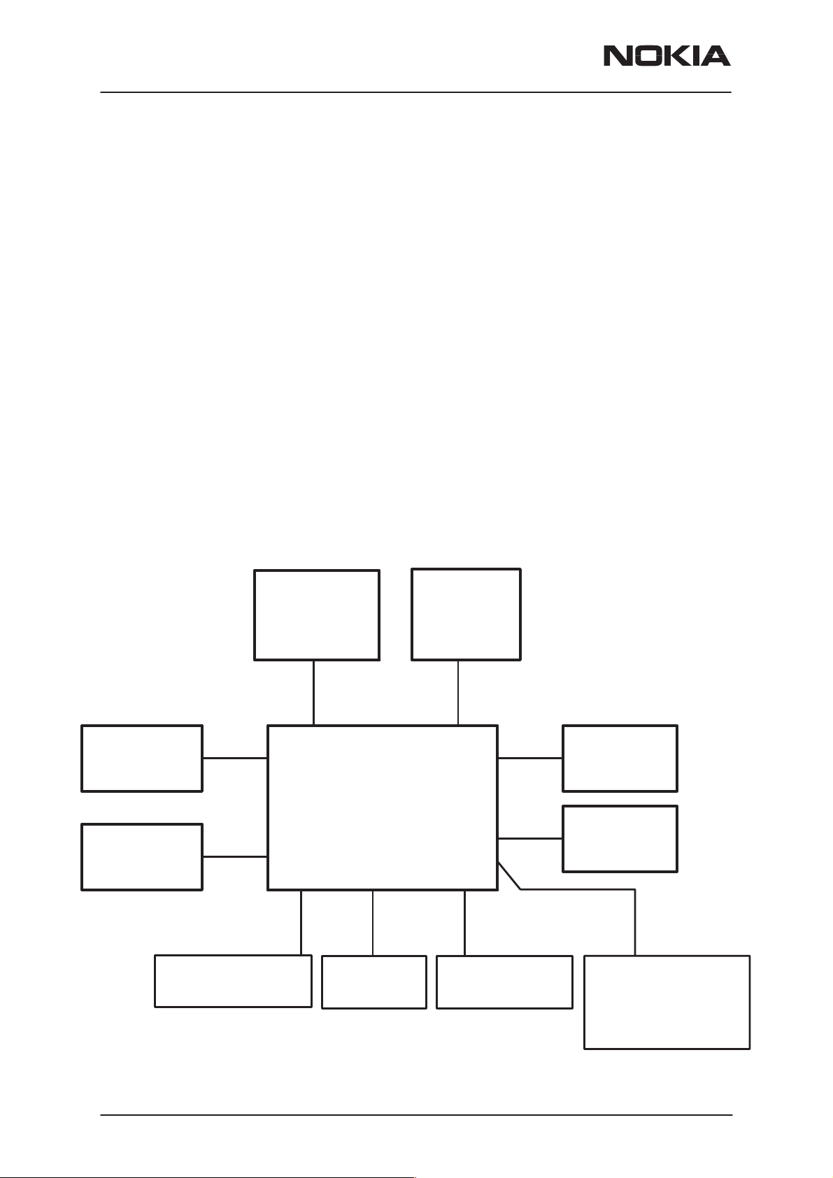
Interconnection Diagram
Keyboard
module
SIM Battery
Radio
Module
LA5
Antenna
Display
Charger
Page 6
MIC
IR Link
Nokia Corporation
Earpiece
HF
+
FM antenna
Issue 1 02/2002
Page 7
PAMS Technical Documentation
System Module LA5
Baseband Module
The baseband architecture supports a power saving function called ”sleep
mode”. This sleep mode shuts off the VCTCXO, which is used as system
clock source for both RF and baseband. During the sleep mode the sys-
tem runs from a 32 kHz crystal. The phone is waken up by a timer run-
ning from this 32 kHz clock supply. The sleep time is determined by net-
work parameters. Sleep mode is entered when both the MCU and the
DSP are in standby mode and the normal VCTCXO clock is switched off.
NPM–9 supports both three and two wire type of Nokia chargers. Three
wire chargers are treated like two wire ones. There is not separate PWM
output for controlling charger but it is connected to GND inside the bottom
connector. Charging is controlled by UEM ASIC (Universal Energy Man-
agement) and EM SW running in the UPP (Universal Phone Processor).
NPM–9
System Module & UI
BLB–2 Li–ion battery is used as main power source for the phone.
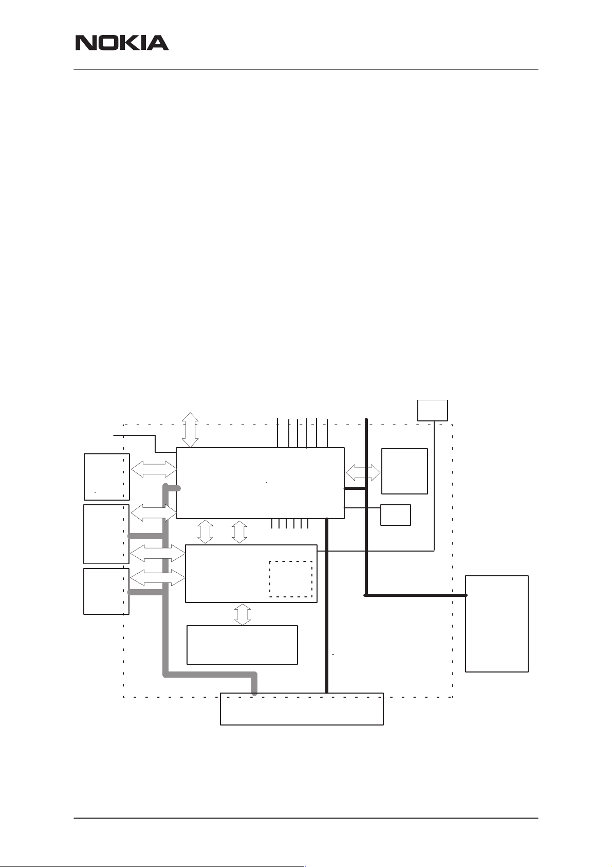
Block Diagram
TX/RX SIGNALS
PWR
IR
FM
radio
UI
Digital Control
UPP
FLASH MEMORY
RF SUPPLIES
UEM
BB SUPPLIES
RAM
PA SUPPL Y
32kHz
CLK
SLEEP CLOCK
SIM
VBAT
13MHz
CLK
SYSTEM CLOCK
BATTERY
BASEBAND
UPP ASIC (Universal Phone Processor) provides the MCU, DSP, external
memory interface and digital control functions. UEM ASIC (Universal En-
ergy Management) contains power supply circuitry, charging, audio proc-
essing and RF control hardware.
Issue 1 02/2002
EXT. AUDIO
HS–connector
Charger
connector
Nokia Corporation
Page 7
Page 8

NPM–9
System Module & UI
Technical Summary
Baseband is running from power rails 2.8V analog voltage and 1.8V I/O
voltage. UPP core voltage Vcore can be lowered down to 1.0V, 1.3V and
1.5V. UEM includes 6 linear LDO (low drop–out) regulators for baseband
and 7 regulators for RF. It also includes 4 current sources for biasing pur-
poses and internal usage. UEM also includes SIM interface which has
supports both 1.8V and 3V SIM cards.
Note: 5V SIM cards are no longer supported by NPM–9 baseband.
A real time clock function is integrated into the UEM which utilizes the
same 32kHz clock supply as the sleep clock. A backup power supply is
provided for the RTC which keeps the real time clock running when the
main battery is removed. The backup power supply is a rechargeable sur-
face mounted capacitor. The backup time with the capacitor is 30 minutes
minimum.
The analog interface between the baseband and the RF section is han-
dled by a UEM ASIC. UEM provides A/D and D/A conversion of the in–
phase and quadrature receive and transmit signal paths and also A/D and
D/A conversions of received and transmitted audio signals to and from
the user interface. The UEM supplies the analog TXC and AFC signals to
RF section according to the UPP DSP digital control. Data transmission
between the UEM and the UPP is implemented using two serial busses,
DBUS for DSP and CBUS for MCU. RF ASIC, Hagar, is controlled
through UPP RFBUS serial interface. There is also separate signals for
PDM coded audio. Digital speech processing is handled by the DSP in-
side UPP ASIC. UEM is a dual voltage circuit, the digital parts are running
from the baseband supply 1.8V and the analog parts are running from the
analog supply 2.78V also VBAT is directly used by some blocks.
PAMS Technical Documentation
The baseband supports both internal and external microphone inputs and
speaker outputs. UEM also includes third microphone input which is used
in NPM–9 for FM radio. Input and output signal source selection and gain
control is done by the UEM according to control messages from the UPP.
Keypad tones, DTMF, and other audio tones are generated and encoded
by the UPP and transmitted to the UEM for decoding. A buzzer and exter-
nal vibra alert control signals are generated by the UEM with separate
PWM outputs.
NPM–9 has two external serial control interfaces: FBUS and MBUS.
These busses can be accessed only through production test pattern.
EMC shielding for baseband is implemented using a metallized plastic
frame and UI PWB ground plane. On the other side the engine is shielded
with PWB grounding. Heat generated by the circuitry will be conducted
out via the PWB ground planes.
NPM–9 radio module is implemented to 8 layer PWB. UI module is divid-
ed between main PWB LA5 and separate UI PWB LU9.
Page 8
Nokia Corporation
Issue 1 02/2002
Page 9
PAMS Technical Documentation
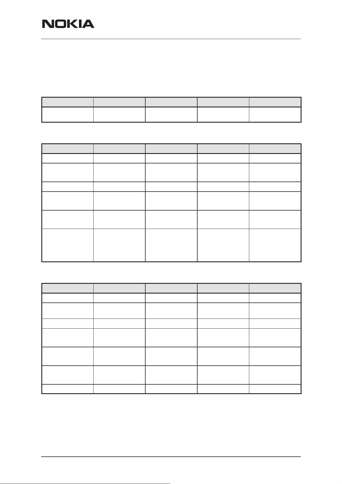
DC Characteristics
Regulators and Supply Voltage Ranges
Battery Voltage Range
Signal Min Nom Max Note
NPM–9
System Module & UI
VBAT 3.1V 3.6V 4.2V (charging
high limit voltage)
BB Regulators
Signal Min Nom Max Note
VANA 2.70V 2.78V 2.86V I
VFLASH1 2.70V 2.78V 2.86V I
VFLASH2 2.70V 2.78V 2.86V I
VSIM 1.745V
2.91V
1.8V
3.0V
1.855V
3.09V
VIO 1.72V 1.8V 1.88V I
VCORE 1.0V
1.235V
1.425V
1.710V
1.053V
1.3V
1.5V
1.8V
1.106V
1.365V
1.575V
1.890V
RF Regulators
3.1V SW cut off
= 80mA
max
= 70mA
max
I
= 1.5mA
Sleep
= 40mA
max
I
= 25mA
max
I
= 0.5mA
Sleep
= 150mA
max
I
= 0.5mA
Sleep
I
= 200mA
max
I
= 0.2mA
Sleep
Default value =
1.5V
Signal Min Nom Max Note
VR1A 4.6V 4.75V 4.9V I
VR2 2.70V
3.20V
2.78V
3.3V
2.86V
3.40V
VR3 2.70V 2.78V 2.86V I
VR4 2.70V 2.78V 2.86V I
VR5 2.70V 2.78V 2.86V I
VR6 2.70V 2.78V 2.86V I
VR7 2.70V 2.78V 2.86V I
max
I
max
max
max
I
Sleep
max
I
Sleep
max
I
Sleep
max
= 10mA
= 100mA
= 20mA
= 50mA
= 0.1mA
= 50mA
= 0.1mA
= 50mA
= 0.1mA
= 45mA
Issue 1 02/2002
Nokia Corporation
Page 9
Page 10
NPM–9
System Module & UI
PAMS Technical Documentation
External and Internal Signals and Connections
This section describes the external and internal electrical connection and
interface levels on the baseband. The electrical interface specifications
are collected into tables that covers a connector or a defined interface.
Internal Signals and Connections
FM Radio Interface
BB Signal FM Radio
Signal
VFLASH2
GenIO(3) FMClk
GenIO(8) FMWrEn
Vcc1 2.7V 2.78V 2.86V max. Icc1
Vcc2 2.7V 2.78V 2.86V max. Icc2
VDD 2.7V 2.78V 2.86V max. IDD
Min Nom Max Condition Note
19mA
800uA
3mA
1.4V
0
30ppm Stability
1.4V
0V
20µs t
1.8V 1.88V
0.4V
75581 kHz Frequency In GSM
2 µs t
1.8V 1.88V
0.4V
High
Low
rise
High
Low
wd
Reference
clock for FM
radio module
rise / fall time
FMWrEn
before rising
edge of
FMCtrlClk
(write operation)
high
GenIO(11) FMCtrlClk
Page 10
1.4V
0
50 ms t
1.8V 1.88V
0.4V
1 µs tr / t
Nokia Corporation
High
Low
start
max. 300kHz
f
rise / fall time
FMCtrlClk
delay after
switching on
the VFLASH2
(oscillator running)
Issue 1 02/2002
Page 11
PAMS Technical Documentation
out ut
NPM–9
System Module & UI
BB Signal
Signal
GenIO(12) FMCtrlDa
1.4V
0
10 µs t
1.5 µs t
GenIO(27) FMTuneX 1.4V
0
1.8V 1.88V
0.4V
14us t
1.8V 1.88V
0.4V
High
Low
da
shift
hold
High
Low
NoteConditionMaxNomMinFM Radio
Bidirectional
shift register
available after
”search
ready”
data available
after
FMCtrlClk
rising edge (read
operation)
FMCtrlDa
sta-
bile after
FMCtrlClk
rising edge
(write operation)
from FM module to UPP
(FMCtrlClk =
’1’)
MIC3P FMAudio
228mV
pp
326mV
pp
460mV
pp
50dB S/N
2% Harmonic
Internal microphone
Signal Min Nom Max Condition Note
MICP
200mV
pp
2.0 V 2.1 V 2.25 V DC
MICN 2.0V 2.1V 2.25V DC
Internal speaker
Signal Min Nom Max Condition Note
EARP
0.75V 0.8V
EARN
0.75V 0.8V
2.0 V
0.85V
2.0 V
0.85V
pp
pp
distortion
AC
AC
DC
AC
DC
2.2kΩ to
MIC1B
Differential
p
(V
= 4.0
diff
Vpp)
Issue 1 02/2002
Nokia Corporation
Page 11
Page 12
NPM–9
04V
tracks and ferrites
f
CO
Current
2 10
mA
tu
tuning
Su
Su ly for TX
VLO
buffers, rescaler
System Module & UI
PAMS Technical Documentation
AC and DC Characteristics of RF–BB voltage supplies
Signal
name
VBAT Battery PA & UEM
VR1A UEM VCP
VR2 UEM VRF_TX
VR3 UEM VCTCXO
From To Parameter Min Typ Max Unit Function
Voltage 2.95 3.6 4.2 V
Current 2000 mA
Current drawn by
PA when ”off”
Voltage 4.6 4.75 4.9 V
Noise density 240 nVrms/
Voltage 2.70 2.78 2.86 V
Current 65 100 mA
Noise density
f=100Hz
f>300Hz
Voltage 2.70 2.78 2.86 V
0.8 2 uA
sqrt(Hz)
120 nVrms/
sqrt(Hz)
Battery supply .
Cut–off level of
regulators is 3.
Losses in pwb
tracks and ferrites
are taken account to
minimum battery
voltage level.
Supply for varactor
or UHF V
ning.
.
Supply for part of
transmit strip.
pply for TX
I/Q–modulators.
Supply for VCTCXO
.
VR4 UEM VRF_RX
VR5 UEM VDIG,
VPRE,
VL
VR6 UEM VBB
Current 1 20 mA
Noise density 240 nVrms/
sqrt(Hz)
Voltage 2.70 2.78 2.86 V
Current 50 mA
Noise density
f = 6 Hz
f = 60 Hz
f 600Hz
Voltage 2.70 2.78 2.86 V
Current 50 mA
Noise density
BW=100Hz...
100kHZ
Voltage 2.70 2.78 2.86 V
Current 50 mA
Noise density
BW=100Hz...
100kHz
5500
240 nVrms/
240 nVrms/
550
55
nVrms/
sqrt(Hz)
sqrt(Hz)
sqrt(Hz)
Supply for Hagar
RX; preamp., mixer,
DTOS
Noise density
decades 20dB/dec
from 6Hz to 600Hz.
From f >600Hz
maximum noise
density
RMS
/√Hz.
l
r
,
55nV
Supply for Hagar
PLL; dividers, LO–
ffr pr
Supply for Hagar
BB and LNA
Page 12
Nokia Corporation
Issue 1 02/2002
Page 13

PAMS Technical Documentation
CO
for RF–IC
density is
some digita
some digital arts of
Signal name
FromToParameter
Fun
ter
DC
ng?
name
VR7 UEM UHF VCO
System Module & UI
Voltage 2.70 2.78 2.86 V
Current 30 mA
NPM–9
FunctionUnitMaxTypMinParameterToFromSignal
Supply for UHF
V
VrefRF01 UEM VREF_RX
VrefRF02 UEM VB_EXT
Noise density
100Hz<f<2kHz
2kHz<f<10kHz
10kHz<f<30kHz
30kHz<f<90kHz
90kHz<f<3MHz
Voltage 1.334 1.35 1.366 V
Current 100 uA
Temp Coef –65 +65 uV/C
Noise density
BW=600Hz...
100kHz Note
Voltage 1.323 1.35 1.377 V
Current 100 uA
Temp Coef –65 +65 uV/C
Noise density
BW=100Hz...
100kHz
70
nVrms/
55
sqrt(Hz)
35
30
30
60 nVrms/
sqrt(Hz)
350 nVrms/
sqrt(Hz)
Voltage Reference
.
Note: Below
600Hz noise
allowed to
increase 20
dB/oct
Supply for RF–BB
digital interface and
l parts of
RF.
AC and DC Characteristics of RF–BB digital signals
Min Typ Max Unit
TXP
(RFGenOut3)
UPP PA &
RF–IC
”1” 1.38 1.88 V
”0” 0 0.4 V
Load Resistance 10 220 kohm
Load Capacitance 20 pF
Timing Accuracy 1/4 symbol
Input Characteristics
c-
tion
Tran
smit
ter
pow
er
amp
lifier
ena
ble /
N2
timi
??
Issue 1 02/2002
Nokia Corporation
Page 13
Page 14

NPM–9
ena
ena
data
data
d
cloc
cloc
(G
)
ag
Hag
circuits, AC
circuits, AC
System Module & UI
PAMS Technical Documentation
RFBusEna1X UPP RF–IC
RFBusData UPP RF–IC
RFBusClk UPP RF–IC
ParameterToFromSignal name
UnitMaxTypMin
”1” 1.38 1.88 V
”0” 0 0.4 V
Current 50 uA
Load resistance 10 220 kohm
Load capacitance 20 pF
”1” 1.38 1.88 V
”0” 0 0.4 V
Load resistance 10 220 kohm
Load capacitance 20 pF
Data frequency 10 MHz
”1” 1.38 1.88 V
”0” 0 0.4 V
Load resistance 10 220 kohm
Load capacitance 20 pF
Data frequency 10 MHz
Fun
c-
tion
RFb
us
ble
RFb
us
;
rea
/writ
e
RFb
us
k
RESET
ENIO6
UPP RF–IC
”1” 1.38 1.85 V
”0” 0 0.4 V
Load capacitance 20 pF
Load resistance 10 220 kohm
Timing accuracy 1/4 symbol
Res
et to
H
ar
AC and DC Characteristics of RF–BB analogue signals
Signal name From To Parameter Min Typ Max Unit Function
VCTCXO VCTCXO UPP
VCTCXOGnd VCTXO UPP DC Level 0 V Ground for
Signal amplitude 0.2 0.8 2.0 Vpp
Input Impedance 10 kohm
Input Capacitance 10 pF
Harmonic Content –8 dBc
Clear signal
window (no glitch)
Duty Cycle 40 60 %
200 mVpp
High stability clock
signal for the logic
coupled. Distorted
sine wave eg.
sawtooth.
reference clock
RXI/RXQ RF–IC UEM
Page 14
Nokia Corporation
Differential voltage
swing (static)
DC level 1.3 1.35 1.4 V
I/Q amplitude
missmatch
I/Q phase
missmatch
1.35 1.4 1.45 Vpp
0.2 dB
–5 5 deg
Issue 1 02/2002
RX baseband
signal.
Page 15

PAMS Technical Documentation
Programmable
voltage
opa
oam G1
NPM–9
System Module & UI
FunctionUnitMaxTypMinParameterToFromSignal name
TXIP / TXIN UEM RF–IC
TXQP /
TXQN
AFC UEM VCTCXO
Aux_DAC
(TxC)
UEM RF–IC Same spec as for TXIP / TXIN Differential
UEM RF
Differential voltage
swing (static)
DC level 1.17 1.20 1.23 V
Source
Impedance
Voltage Min
Max
Resolution 11 bits
Load resistance
and capacitance
Step settling time 0.2 ms
Voltage Min
Max 2.4
Source
Impedance
Resolution 10 bits
2.23 2.48 Vpp
200 ohm
0.0
2.4
1
0.1
V
2.6
kohm
100
nF
0.1 V
200 ohm
Programmable
voltage swing.
common mode
.
Between
TXIP–TXIN
quadrature phase
TX baseband
signal for the RF
modulator
Automatic
frequency control
signal for
VCTCXO
Transmitter power
control
Noise density
BW=100Hz...
100kHz
Temp Coef –65 +65 uV/C
RFTemp RF UEM
Vbase RF UEM Voltage 2.7 V Detected voltage
Voltage at –20oC 1,57
Voltage at +25oC 1,7
Voltage at +60oC 1,79
800 nVrms/
sqrt(Hz)
V Temperature
NOTE; Assumed
power control
mp G=1
sensor of RF.
from PA power
level sensing unit
External Signals and Connections
UI (board–to–board) connector
Pin Signal Min Nom Max Condition Note
1 SLOWAD(2) 1.5V
0.1V
2 VBAT 3.0V 3.6V 4.2V Battery voltage
3 ROW(4) 0.7xVIO
0
2.7V
1.0V
1.8V
0.3xVIO
Flip closed
Flip open
High
Low
used for flip
identification
for leds
Keyboard ma-
trix row 4
Issue 1 02/2002
Nokia Corporation
Page 15
Page 16

NPM–9
System Module & UI
PAMS Technical Documentation
NoteConditionMaxNomMinSignalPin
4 ROW(3) 0.7xVIO
0
5 COL(2) 0.7xVIO
0
6 ROW(2) 0.7xVIO
0
7 COL(1) 0.7xVIO
0
8 ROW(0) 0.7xVIO
0
9 KLIGHT VBAT
10 ROW(1) 0.7xVIO
0
11 COL(3) 0.7xVIO
0
12 COL(4) 0.7xVIO
0
13 GND 0V
14 GND 0V
15 GND 0V
VIO
0.3xVIO
VIO
0.3xVIO
VIO
0.3xVIO
VIO
0.3xVIO
VIO
0.3xVIO
0.3xVBAT
VIO
0.3xVIO
VIO
0.3xVIO
VIO
0.3xVIO
High
Low
High
Low
High
Low
High
Low
High
Low
LED off
LED on
High
Low
High
Low
High
Low
Keyboard matrix row 3
Keyboard matrix column 2
Keyboard matrix row 2
Keyboard matrix column 1
Keyboard matrix row 0
two colour led
control
Keyboard matrix row 1
Keyboard matrix column 3
Keyboard matrix column 4
16 GND 0V
LCD connector
Pin Signal Min Nom Max Condition Note
1 XRES
2 XCS
3 GND 0V
4 SDA
0.8*VIO
0
100ns t
0.8*VIO
0
130ns t
130ns t
300ns t
0.8*VIO
0
0.7*VIO
0
100ns t
100ns t
VIO
0.22*VIO
VIO
0.22*VIO
VIO
0.22*VIO
VIO
0.3*VIO
Logic ’1’
Logic ’0’
rw
Logic ’1’
Logic ’0’
css
csh
csw
Logic ’1’
Logic ’0’
Logic ’1’
Logic ’0’
sds
sdh
Reset
Active low
Reset active
Chip select
Active low
XCS low before
SCLK rising
edge
XCS low after
SCLK rising
edge
XCS high pulse
width
Serial data
(driver input)
Serial data
(driver output)
Data setup time
Data hold time
Page 16
Nokia Corporation
Issue 1 02/2002
Page 17

NPM–9
PAMS Technical Documentation
5 SCLK
6 VDDI (VIO) 1.72V 1.8V 1.88V Logic voltage
7 VDD
(VFLASH1)
8 VOUT 9V Booster output,
0.8*VIO
0
250ns t
1 10ns t
1 10ns t
VIO
0.22*VIO
4.0MHz
Logic ’1’
Logic ’0’
Max frequency
scyc
shw
slw
2.72V 2.78V 2.86V Voltage supply
System Module & UI
NoteConditionMaxNomMinSignalPin
Serial clock input
Clock cycle
Clock high
Clock low
supply
Connected to
VIO
Connected to
VFLASH1
C=1uF connected to GND
DC connector
Pin Signal Min Nom Max Condition Note
2 VCHAR 7.0 V
RMS
8.4 V
RMS
9.2 V
RMS
850 mA
Fast charger
Charger positive input
1 CHGND 0 Charger ground
Headset connector
Pin Signal Min Nom Max Condition Note
5 XMICP
3 XMICN
4 XEARN
7 XEARP
1V
pp
100 mV
2.0 V 2.1 V 2.25 V DC
1V
pp
100 mV
0.75V 0.8V 0.85V DC
1V
pp
0.75V 0.8V 0.85V DC
pp
pp
G = 0dB
G = 20dB
G = 0 dB
G = 20dB
AC
1kΩ to MIC2B
1kΩ to GND
1V
5 HookInt 0V 2.86V
(VFLASH1)
6 HeadInt 0V 2.86V
(VANA)
Issue 1 02/2002
Nokia Corporation
pp
AC
Connected to
UEM AD–converter
Accessory
detection
Page 17
Page 18

NPM–9
System Module & UI
PAMS Technical Documentation
SIM connector
Pin Name Parameter Min Typ Max Unit Notes
1 VSIM
2 SIMRST
3 SIMCLK
4 DATA
1.8V SIM Card 1.6 1.8 1.9
3V SIM Card 2.8 3.0 3.2
1.8V SIM Card 0.9xVSIM
0
3V SIM Card 0.9xVSIM
0
Frequency 3.25 MHz
Trise/Tfall 50 ns
1.8V Voh
1.8V Vol
3 Voh
3 Vol
1.8V Voh
1.8V Vol
3 Voh
3 Vol
1.8V Vih
1.8V Vil
3V Vil
3V Vil
0.9xVSIM
0
0.9xVSIM
0
0.9xVSIM
0
0.9xVSIM
0
0.7xVSIM
0
0.7xVSIM
0
VSIM
0.15xVSIM
VSIM
0.15xVSIM
VSIM
VSIM
VSIM
0.15xVSIM
VSIM
0.15xVSIM
VSIM
0.15xVSIM
VSIM
0.15xVSIM
V Supply voltage
V SIM reset (output)
V
V SIM data (output)
SIM clock
SIM data (input)
Trise/Tfall max 1us
5 NC
6 GND GND 0 V Ground
Page 18
Nokia Corporation
Issue 1 02/2002
Page 19

PAMS Technical Documentation
Functional Description
Modes of Operation
LA5 baseband engine has six different operating modes:
– No supply
– Backup
– Acting Dead
– Active
– Sleep
– Charging
No supply
In NO_SUPPLY mode the phone has no supply voltage. This mode is due
to disconnection of main battery and backup battery or low battery voltage
level in both of the batteries.
Phone is exiting from NO_SUPPLY mode when sufficient battery voltage
level is detected. Battery voltage can rise either by connecting a new bat-
Backup
tery with VBAT > V
tery above V
MSTR+
MSTR+
.
NPM–9
System Module & UI
or by connecting charger and charging the bat-
In BACKUP mode the backup battery has sufficient charge but the main
battery can be disconnected or empty (VBAT < V
VBU
VRTC regulator is disabled in BACKUP mode. VRTC output is supplied
without regulation from backup battery (VBACK). All the other regulators
are disabled.
Acting Dead
If the phone is off when the charger is connected, the phone is powered
on but enters a state called ”Acting Dead”. To the user the phone acts as
if it was switched off. A battery charging alert is given and/or a battery
charging indication on the display is shown to acknowledge the user that
the battery is being charged.
Active
In the active mode the phone is in normal operation, scanning for channels, listening to a base station, transmitting and processing information.
There are several sub–states in the active mode depending on if the
phone is in burst reception, burst transmission, if DSP is working etc.
One of the sub–state of the active mode is FM radio on state. In that case
UEM audio blocks and FM radio are powered on. FM radio circuitry is
controlled by the MCU and 75kHz reference clock is generated in the
UPP. VFLASH2 regulator is operating.
COFF
MSTR
and VBACK >
).
In active mode the RF regulators are controlled by SW writing into UEM’s
registers wanted settings: VR1A can be enabled or disabled. VR2 can be
enabled or disabled and its output voltage can be programmed to be
Issue 1 02/2002
Nokia Corporation
Page 19
Page 20

NPM–9
System Module & UI
2.78V or 3.3V. VR4 –VR7 can be enabled or disabled or forced into low
quiescent current mode. VR3 is always enabled in active mode.
Sleep mode
Sleep mode is entered when both MCU and DSP are in stand–by mode.
Sleep is controlled by both processors. When SLEEPX low signal is detected UEM enters SLEEP mode. VCORE, VIO and VFLASH1 regulators
are put into low quiescent current mode. All RF regulators are disabled in
SLEEP. When SLEEPX=1 is detected UEM enters ACTIVE mode and all
functions are activated.
The sleep mode is exited either by the expiration of a sleep clock counter
in the UEM or by some external interrupt, generated by a charger connection, key press, headset connection etc.
In sleep mode VCTCXO is shut down and 32 kHz sleep clock oscillator is
used as reference clock for the baseband.
Charging
PAMS Technical Documentation
The battery voltage, temperature, size and current are measured by the
UEM controlled by the charging software running in the UPP.
The charging control circuitry (CHACON) inside the UEM controls the
charging current delivered from the charger to the battery. The battery
voltage rise is limited by turning the UEM switch off when the battery voltage has reached 4.2 V. Charging current is monitored by measuring the
voltage drop across a 220 mOhm resistor.
Supply Voltage Regulation
Supply voltage regulation is controlled by UEM asic. There are six separate regulators used by baseband block.
BB Regulators
Signal Min Nom Max Note
VANA 2.70V 2.78V 2.86V I
VFLASH1 2.70V 2.78V 2.86V I
VFLASH2 2.70V 2.78V 2.86V I
VSIM 1.745V
2.91V
VIO 1.72V 1.8V 1.88V I
VCORE 1.0V
1.235V
1.425V
1.710V
1.8V
3.0V
1.053V
1.3V
1.5V
1.8V
1.855V
3.09V
1.106V
1.365V
1.575V
1.890V
= 80mA
max
= 70mA
max
I
= 1.5mA
Sleep
= 40mA
max
I
= 25mA
max
I
= 0.5mA
Sleep
= 150mA
max
I
= 0.5mA
Sleep
I
= 200mA
max
I
= 0.2mA
Sleep
Default value =
1.5V
Page 20
Nokia Corporation
Issue 1 02/2002
Page 21

PAMS Technical Documentation
Battery
Li–ion battery pack BLB–2 is used in NPM–9.
Nominal discharge cut–off voltage 3.1V
Nominal battery voltage 3.6V
Nominal charging voltage 4.2V
Pin numbering of battery pack
Signal name Pin number Function
VBAT 1 Positive battery terminal
BSI 2 Battery capacity measurement (fixed resistor inside the
BTEMP 3 Battery temperature measurement (measured by ntc
GND 4 Negative/common battery terminal
NPM–9
System Module & UI
battery pack)
resistor inside pack)
BLB–2 battery pack pin order
Power Up and Reset
Power up and reset is controlled by the UEM ASIC. NPM–9 baseband
can be powered up in following ways:
1. Press power button which means grounding the PWRONX pin of the
UEM
2. Connect the charger to the charger input
3. Supply battery voltage to the battery pin
4. RTC Alarm, the RTC has been programmed to give an alarm
1 (+)2(BSI)3(BTEMP)4(GND)
After receiving one of the above signals, the UEM counts a 20ms delay
and then enters it’s reset mode. The watchdog starts up, and if the battery
voltage is greater than Vcoff+ a 200ms delay is started to allow references etc. to settle. After this delay elapses the VFLASH1 regulator is enabled. 500us later VR3, VANA, VIO and VCORE are enabled. Finally the
PURX (Power Up Reset) line is held low for 20 ms. This reset, PURX, is
fed to the baseband ASIC UPP, resets are generated for the MCU and
Issue 1 02/2002
Nokia Corporation
Page 21
Page 22

NPM–9
System Module & UI
the DSP. During this reset phase the UEM forces the VCTCXO regulator
on regardless of the status of the sleep control input signal to the UEM.
The FLSRSTx from the ASIC is used to reset the flash during power up
and to put the flash in power down during sleep. All baseband regulators
are switched on at the UEM power on except SIM and VFLASH2 regulators which are controlled by the MCU. The UEM internal watchdogs are
running during the UEM reset state, with the longest watchdog time selected. If the watchdog expires the UEM returns to power off state. The
UEM watchdogs are internally acknowledged at the rising edge of the
PURX signal in order to always give the same watchdog response time to
the MCU.
A/D Channels
The UEM contains the following A/D converter channels that are used for
several measurement purpose. The general slow A/D converter is a 10 bit
converter using the the UEM interface clock for the conversion. An interrupt will be given at the end of the measurement.
PAMS Technical Documentation
The UEM’s 11–channel analog to digital converter is used to monitor
charging functions, battery functions, voltage levels in external accessory
detection inputs, user interface and RF functions.
When the conversion is started the converter input is selected. Then the
signal processing block creates a data with MSB set to ’1’ and and others
to ’0’. In the D/A converter this data controls the switches which connect
the input reference voltage (VrefADC) to the resistor network. The generated output voltage is compared with the input voltage under measurement and if the latter is greater, MSB remains ’1’ else it is set ’0’. The following step is to test the next bit and the next...until LSB is reached. The
result is then stored to ADCR register for UPP to read.
The monitored battery functions are battery voltage (VBATADC), battery
type (BSI) and battery temperature (BTEMP) indication.
The battery type is recognized through a resistive voltage divider. In
phone there is a 100kOhm pull up resistor in the BSI line and the battery
has a pull down resistor in the same line. Depending on the battery type
the pull down resistor value is changed. The battery temperature is measured equivalently except that the battery has a NTC pull down resistor in
the BTEMP line.
KEYB1&2 inputs are used for keyboard scanning purposes. These inputs
are also routed internally to the miscellaneous block. In NPM–9 KEYB1
input is used for flip detection.
Page 22
The HEADINT and HOOKINT are external accessory detection inputs
used for monitoring voltage levels in these inputs. They are routed internally from the miscellaneous block and they are connected to the converter through a 2/1 multiplexer.
The monitored RF functions are PATEMP and VCXOTEMP detection. PATEMP input is used to measure temperature of the RFIC, Hagar. VCXOTEMP is not used in NPM–9.
Nokia Corporation
Issue 1 02/2002
Page 23

PAMS Technical Documentation
FM Radio
FM radio circuitry is implemented using highly integrated radio IC,
TEA5757. Only few external components like filters, discriminator and capacitors are needed.
TEA5757 is an integrated AM/FM stereo radio circuit including digital tuning and control functions. NPM–9 radio is implemented as superheterodyne FM mono receiver. FM stage of the TEA5757 incorporates a tuned
RF stage, a double balanced mixer, one pin oscillator and is designed for
distributed IF ceramic filters. IF frequency is 10.7 MHz.
Channel tuning and other controls are controlled by the MCU. Reference
clock, 75kHz, is generated by the UPP CTSI block.
FM radio circuitry is controlled through serial bus interface by the MCU
SW. TEA5757 informs MCU when channel is tuned by setting
signal to logic ’0’.
Digital Interface
NPM–9
System Module & UI
FMTuneX
UPP TEA5757
GenIO(3)
GenIO(12)
GenIO(11)
GenIO(8)
GenIO(27)
NOTE:
FMCtrlClk
needs to be set to logic ’1’ when data is not written or
FMClk
FMCtrlDa
FMCtrlClk
FMWrEn
FMTuneX
read. This is required for correct operation of the
FM radio audio & antenna connections
Bottom
Connector
1000Ω@100MHz
XTAL
VIO
DATA
BUS–CLK
WR–EN
VIO
MO/ST
FMTuneX
signal.
UEM TEA5757
XEARP
XEARN
Issue 1 02/2002
1n
1n
18pF18pF
72nH
Nokia Corporation
HF
MIC3
HFCM
100nF
3.9nF
4.7kΩ
AFLO
100kΩ
FM_RFI
Page 23
Page 24

NPM–9
System Module & UI
IR Module
The IR interface, when using 2.7V transceiver, is designed into the UEM.
The IR link supports speeds from 9600 bit/s to 1.152 MBit/s up to distance of 1m. Transmission over the IR if half–duplex.
The lenght of the transmitted IR pulse depends on the speed of the transmission. When 230.4 kbit/s or less is used as a transmission speed, pulse
length is maximum 1.63us. If transmission speed is set to 1.152Mbit/s the
pulse length is 154ns according to IrDA specification.
Backup Battery
Backup battery is used in case when main battery is either removed or
discharged. Backup battery is used for keeping real-time clock running for
minimum of 30 minutes.
Rechargeable backup battery is connected between UEM VBACK and
GND. In UEM backup battery charging high limit is set to 3.2V. The cut–
off limit voltage (V
charging is controlled by MCU by writing into UEM register.
BUCoff–
PAMS Technical Documentation
) for backup battery is 2.0V. Backup battery
Polyacene SMD battery type is used. The nominal capacity of the battery
is 0.2 mAh.
SIM Interface
UEM contains the SIM interface logic level shifting. SIM interface can be
programmed to support 3V and 1.8V SIMs. SIM supply voltage is selected by a register in the UEM. It is only allowed to change the SIM supply voltage when the SIM IF is powered down.
The SIM power up/down sequence is generated in the UEM. This means
that the UEM generates the RST signal to the SIM. Also the SIMCardDet
signal is connected to UEM. The card detection is taken from the BSI signal, which detects the removal of the battery. The monitoring of the BSI
signal is done by a comparator inside UEM. The comparator offset is
such that the comparator output do not alter state as long as the battery
is connected. The threshold voltage is calculated from the battery size
specifications.
The SIM interface is powered up when the SIMCardDet signal indicates
”card in”. This signal is derived from the BSI signal.
Parameter Variable Min Typ Max Unit
SIMCARDet, BSI comparator Threshold Vkey 1.94 2.1 2.26 V
SIMCARDet, BSI comparator Hysteresis (1) Vsimhyst 50 75 100 mV
The whole SIM interface locates in two chip UPP and UEM.
The SIM interface in the UEM contains power up/down, port gating, card
detect, data receiving, ATR–counter, registers and level shifting buffers
logic. The SIM interface is the electrical interface between the Subscriber
Identity Module Card (SIM Card) and mobile phone (via UEM device).
Page 24
Nokia Corporation
Issue 1 02/2002
Page 25

PAMS Technical Documentation
The data communication between the card and the phone is asynchronous half duplex. The clock supplied to the card is in GSM system 1.083
MHz or 3.25 MHz. The data baud rate is SIM card clock frequency divided by 372 (by default), 64, 32 or 16. The protocol type, that is supported, is T=0 (asynchronous half duplex character transmission as defined in ISO 7816–3).
NPM–9
System Module & UI
SIM
C5 C6 C7
C1C2C3
From Battery Type contact
C8
C4
The internal clock frequency from UPP CTSI block is 13 MHz in GSM.
Thus to achieve the minimum starting SIMCardClk rate of 3.25 MHz (as is
required by the authentication procedure and the duty cycle requirement
of between 40% and 60%) then the slowest possible clock supplied to the
SIM has to be in the GSM system clock rate of 13/4 MHz.
SIMDATA
SIMCLK
VSIM
BSI
SIMRST
GND
UEM
SIMIF
register
SIMIO
SIMClk
Data
UEM
digital
logic
GND
SIMIO
SIMClk
Data
UPP
UIF Block
UEMInt
CBusDa
CBusEnX
CBusClk
Buzzer
Buzzer is used to generate alerting tones and melodies to indicate incoming call. It is also used to generate keypress and warning tones for the
user. Buzzer is controlled by PWM (Pulse Width Modulation) signal generated by the buzzer driver of the UEM. Target SPL is 100dB (A) at 5cm.
Internal Microphone
The internal microphone capsule is mounted in the bottom connector. Microphone is omnidirectional. The internal microphone is connected to the
UEM microphone input MIC1P/N. The microphone input is asymmetric
and microphone bias is provided by the UEM MIC1B. The microphone
input on the UEM is ESD protected. Spring contacts are used to connect
the microphone contacts to the main PWB.
Issue 1 02/2002
Nokia Corporation
Page 25
Page 26

NPM–9
System Module & UI
UEM
MIC1B
MIC1N
PAMS Technical Documentation
22pF 100nF
33nF
2k2
UPP
33nF
MIC1P
2k2
600Ω@100MHz
27pF
22pF
UPP (Universal Phone Processor) is the digital ASIC of the baseband.
UPP includes 8MBit internal RAM, ARM7 Thump 16/32–bit RISC MCU
core, LEAD3 16–bit DSP core, ROM for MCU boot code and all digital
control logic.
Main functions of the custom logic are:
1. Interface between system logic and MCU/DSP (BodyIf)
2. Clocking, timing, sleep and interrupt block (CTSI) for system
timing control
3. MCU controlled general purpose USART, MBUS USART and
general purpose IOs (PUP).
4. SIM card interface (SIMIf)
5. GSM coder (Coder)
6. GPRS support (GPRSCip)
7. Interfaces for keyboard, LCD and UEM (UIF)
8. Accessory interface for IrDA SIR, IrDA FIR and LPRF (AccIf)
9. SW programmable RF interface (MFI)
10. Programmable serial interface for Hagar RFIC (SCU)
11. Test interface (TestIf)
Memory Block
For the MCU UPP includes ROM, 2 kbytes, that is used mainly for boot
code of MCU. To speed up the MCU operation small 64 byte cache is
also integrated as a part of the MCU memory interface. For program
memory 8Mbit (512 x 16bit) PDRAM is integrated. RAM block can also be
used as data memory and it is byte addressable. RAM is mainly for MCU
purposes but also DSP has also access to it if needed.
Page 26
Nokia Corporation
Issue 1 02/2002
Page 27

PAMS Technical Documentation
MCU code is stored into external flash memory. Size of the flash is 64Mbit
(4096 x 16bit) The NPM–9 baseband supports a burst mode flash with
multiplexed address/data bus. Access to the flash memory is performed
as 16–bit access. The flash has Read While Write capabilities which
makes the emulation of EEPROM within the flash easy.
NPM–9
System Module & UI
Issue 1 02/2002
Nokia Corporation
Page 27
Page 28

NPM–9
System Module & UI
RF Module
This RF module takes care of all RF functions of the engine. RF circuitry
is located on one side (B–side) of the PWB.
EMC leakage is prevented by using a metal B–shield, which screens the
whole RF side (included FM radio) of the engine. The conductive (silicon
or metal) gasket is used between the PWB and the shield. The metal
B–shield is separated to three blocks. The first one include the FM radio.
The second block include the PA, antenna switch, LNAs and dual RX
SAW. The last, but not least, block include the Hagar RF IC, VCO,
VCTCXO, baluns and balanced filters. The blocks are divided on the basis that the attenuation between harmonics of the transmitter and the
VCO signal (including Hagar IC) is a high (over 100dB). The VCO and TX
outputs of the Hagar RF IC are located one another as far as possible. In
order to guard against the radiated spurious inside blocks, the RF transmission lines are made with striplines after PA.
PAMS Technical Documentation
The baseband circuitry is located on the A–side of the board, which is
shielded with a metallized frame and ground plane of the UI–board.
Maximum height inside on B–side is 1.8 mm. Heat generated by the circuitry will be conducted out via the PWB ground planes and metallic
B–shield
RF Frequency Plan
925–960
MHz
1805–1880
MHz
f/4
HAGAR
I–signal
I–signalI–signalI–signal
Q–signal
f
f
RX
f/2f/4
f
f/2
f
3420–
PLL
3840
MHz
Page 28
1710–1785
MHz
880–915
MHz
Nokia Corporation
26 MHz
VCTCXO
I–signal
Q–signal
TX
Issue 1 02/2002
Page 29

PAMS Technical Documentation
DC characteristics
Regulators
Transceiver has a multifunction power management IC on baseband section, which contains among other functions; 7 pcs of 2.78 V regulators
and 4.8V up–switcher for charge pump.
All regulators can be controlled individually with 2.78 V logic directly or
through control register. In GSM direct controls are used to get fast
switching, because regulators are used to enable RF–functions.
Use of the regulators can be seen in the Power Distribution Diagram.
VrefRF01and VrefRF02 are used as the reference voltages for HAGAR
RF–IC, VrefRF01 (1.35V) for bias reference and VrfeRF02 (1.35V) for RX
ADC’s reference.
Regulators (except VR2 and VR7) are connected to HAGAR. Different
modes were switched on by the aid of serial bus.
NPM–9
System Module & UI
List of the needed supply voltages :
Volt. source Load
VR1 PLL charge pump (4,8 V)
VR2 TX modulator
VR3 VCTCXO + buffer
VR4 HAGAR IC (LNAs+mixer+DTOS)
VR5 HAGAR IC (div+LO–buff+prescaler),
VR6 HAGAR (Vdd_bb)
VR7 VCO
VrefRF01 ref. voltage for HAGAR
VrefRF02 ref. voltage for HAGAR
Vbatt PA
Issue 1 02/2002
Nokia Corporation
Page 29
Page 30

NPM–9
System Module & UI
Power Distribution Diagram
PAMS Technical Documentation
SOURCE
VR1
VR2
VR3
VR4
VR5
4.75 V +/– 3.2 %
10 mA
2.78 V +/– 3 %
100 mA
2.78 V +/– 3 %
20 mA
2.78 V +/– 3 %
50 mA
2.78 V +/– 3 %
50 mA
LOAD
Charge pump in HAGAR
TX IQ modulator, power
control opamp in
Hagar
VCTCXO
VCTCXO buffer in Hagar
E–GSM & DCS LNA
RX mixer in Hagar
DTOS in Hagar
PLL in Hagar
UEM
VR6
VR7
VrefRF01
VrefRF02
2.78 V +/– 3 %
50 mA
2.78 V +/– 3 %
50 mA
1.35 v +/– 1.15 %
< 100 ua
1.35 V +/– 2 %
< 100 ua
Dividers in Hagar
LO buffers in Hagar
Prescaler in Hagar
Power detector
BB section in Hagar
SHF VCO Module
Ref. volt. for Hagar RX
Ref. volt. for Hagar
Page 30
VBATT
3.2 – 4.5 V
1700 mA (max)
Nokia Corporation
Dual PA module
Issue 1 02/2002
Page 31

PAMS Technical Documentation
System Module & UI
RF characteristics
Item Values (E–GSM / GSM1800)
Receive frequency range 925 ... 960 MHz / 1805...1880 MHz
Transmit frequency range 880 ... 915 MHz / 1710...1785 MHz
Duplex spacing 45 MHz / 95 MHz
Channel spacing 200 kHz
Number of RF channels 174 / 374
Power class 4 (2 W) / 1 (1 W)
Number of power levels 15 / 16
Transmitter characteristics
Item Values (E–GSM/GSM1800)
Type Direct conversion, nonlinear, FDMA/TDMA
LO frequency range 3520...3660 MHz / 3420...3570 MHz
Output power 2 W / 1 W peak
Gain control range min. 30 dB
Maximum phase error ( RMS/peak ) max 5 deg./20 deg. peak
NPM–9
Receiver characteristics
Item Values, E–GSM/GSM1800
Type Direct conversion, Linear, FDMA/TDMA
LO frequencies 3700...3840 MHz / 3610...3760 MHz
Typical 3 dB bandwidth +/– 91 kHz
Sensitivity min. – 102 dBm (GSM1800 norm.cond. only)
Total typical receiver voltage gain ( from antenna
to RX ADC )
Receiver output level ( RF level –95 dBm ) 230 mVpp, single–ended I/Q signals to RX ADCs
Typical AGC dynamic range 83 dB
Accurate AGC control range 60 dB
Typical AGC step in LNA 30 dB GSM1800 25 dB EGSM
Usable input dynamic range –102 ... –10 dBm
RSSI dynamic range –110 ... –48 dBm
Compensated gain variation in receiving band +/– 1.0 dB
86 dB
Issue 1 02/2002
Nokia Corporation
Page 31
Page 32

Page 32
Nokia Corporation
PCN
Dual SAW
EGSM
LNA
LNA
SAW
SAW
HAGAR
f/2
NPM–9
RF Block Diagram
I
Q
VrefRF01
System Module & UI
f
VrefRF02
CTRL
SERIAL CTRL
BUS
Issue 1 02/2002
ANT SW
Coupler
Dual PA
SAW
PCN
EGSM
f/2
f
PLL
SHF
VCO
f
f/2
13 MHz
f/2
to ASIC
f
f/2
f
26 MHz
VCXO
AFC
TXC
TXP
TXIP
TXIN
TXQP
TXQN
RF_temp
PAMS Technical Documentation
Page 33

PAMS Technical Documentation
Frequency synthesizers
VCO frequency is locked with PLL into stable frequency source, which is
a VCTCXO–module ( voltage controlled temperature compensated crystal
oscillator ). VCTCXO is running at 26 MHz. Temperature drifting is controlled with AFC ( automatic frequency control ) voltage. VCTCXO is
locked into frequency of the base station. AFC is generated by baseband
with a 11 bit conventional DAC. 13MHz VCTCXO can also be used if multislot operations is not needed. If more than 1(RX)+1(TX) slot is wanted
settling times have to be less than 300us from channel to channel. This
can be achieved when PLL loopbandwith is ~35kHz. Noise coming from
the loop and noise from dividers (20*logN) increases rms phase error
over 3 degrees which is the maximum for synthesizer.
R
f
ref
f_out /
M
PHASE
DET.
CHARGE
PUMP
NPM–9
System Module & UI
26 MHz frequency reference
AFC–controlled VCTCXO
LP
f_out
VCO
Kd
M
Kvco
M = A(P+1) + (N–A)P=
= NP+A
PLL is located in HAGAR RF–IC and is controlled via serial RFBus. There
is 64/65 (P/P+1) prescaler, N– and A–divider, reference divider, phase detector and charge pump for the external loop filter. SHF local signal, generated by a VCO–module ( VCO = voltage controlled oscillator ), is fed
thru 180deg balanced phase shifter to prescaler. Prescaler is a dual modulus divider. Output of the prescaler is fed to N– and A–divider, which
produce the input to phase detector. Phase detector compares this signal
to reference signal (400kHz), which is divided with reference divider from
VCTCXO output. Output of the phase detector is connected into charge
pump, which charges or discharges integrator capacitor in the loop filter
depending on the phase of the measured frequency compared to reference frequency.
Loop filter filters out comparison pulses of phase detector and generates
DC control voltage to VCO. Loop filter defines step response of the PLL (
settling time ) and effects to stability of the loop, that’s why integrator capacitor has a resistor for phase compensation. Other filter components
are for sideband rejection. Dividers are controlled via serial bus. RFBusData is for data, RFBusClk is serial clock for the bus and RFBusEna1X is
a latch enable, which stores new data into dividers.
LO–signal is generated by SHF VCO module. VCO has double frequency
in GSM1800 and x 4 frequency in EGSM compared to actual RF channel
Issue 1 02/2002
Nokia Corporation
Page 33
Page 34

NPM–9
System Module & UI
frequency. LO signal is divided by two or four in HAGAR (depending on
system mode).
Receiver
Receiver is a direct conversion, dual band linear receiver. Received RF–
signal from the antenna is fed via RF–antenna switch module to 1st RX
bandpass RF–SAW filters and MMIC LNAs (low noise amplifier). RF–antenna switch module contains upperband and lowerband operation. The
LNA amplified signal is fed to 2nd RX bandpass RF–SAW filters. Both 2
RX bandpass RF–SAW filters have un–bal/bal configuration to get the
balanced (balanced) feed for Hagar.
Discrete LNAs have three gain levels. The first one is max. gain, the second one is about –30dB(GSM1800) and –25dB(EGSM900) below max.
gain and the last one is off state. The gain selection control of LNAs
comes from HAGAR IC.
RX bandpass RF–SAW filters define how good are the blocking characteristics against spurious signals outside passband and the protection
against spurious responses.
PAMS Technical Documentation
nd
Differential RX signal is amplified and mixed directly down to BB frequency in HAGAR. Local signal is generated with external VCO. VCO signal is
divided by 2 (GSM1800) or by 4 (E–GSM900). PLL and dividers are in
HAGAR–IC.
From the mixer output to ADC input RX signal is divided into I– and
Q–signals. Accurate phasing is generated in LO dividers. After the mixer
DTOS amplifiers convert the differential signals to single ended. DTOS
has two gain stages. The first one has constant gain of 12dB and 85kHz
cut off frequency. The gain of second stage is controlled with control signal g10. If g10 is high (1) the gain is 6dB and if g10 is low (0) the gain of
the stage is –4dB.
The active channel filters in HAGAR provides selectivity for channels
(–3dB @ +/–91 kHz typ.). Integrated base band filter is active–RC–filter
with two off–chip capacitors. Large RC–time constants needed in the
channel select filter of direct conversion receiver are produced with large
off–chip capacitors because the impedance levels could not be increased
due to the noise specifications. Baseband filter consists of two stages,
DTOS and BIQUAD. DTOS is differential to single–ended converter having 8dB or 18dB gain. BIQUAD is modified Sallen–Key Biquad.
Integrated resistors and capacitors are tunable. These are controlled with
a digital control word. The correct control words that compensate for the
process variations of integrated resistors and capacitors and of tolerance
of off chip capacitors are found with the calibration circuit.
Page 34
Next stage in the receiver chain is AGC–amplifier, also integrated into HAGAR. AGC has digital gain control via serial mode bus. AGC–stage provides gain control range (40 dB, 10 dB steps) for the receiver and also the
necessary DC compensation. Additional 10 dB AGC step is implemented
in DTOS stages.
Nokia Corporation
Issue 1 02/2002
Page 35

PAMS Technical Documentation
DC compensation is made during DCN1 and DCN2 operations (controlled
via serial bus). DCN1 is carried out by charging the large external capacitors in AGC stages to a voltage which cause a zero dc–offset. DCN2 set
the signal offset to constant value (VrefRF_02 1.35 V). The VrefRF_02
signal is used as a zero level to RX ADCs.
Single ended filtered I/Q–signal is then fed to ADCs in BB. Input level for
ADC is 1.45 Vpp max.
Rf–temp port is intended to be used for compensation of RX SAW filters
thermal behavior. This phenomena will have impact to RSSI reporting accuracy. The current information is –35ppm/C for center frequency drift
for all bands. This temperature information is a voltage over two diodes
and diodes are fed with constant current.
Transmitter
Transmitter chain consists of two final frequency IQ–modulators for upper
and lower band, a dual power amplifier and a power control loop.
NPM–9
System Module & UI
I– and Q–signals are generated by baseband. After post filtering (RC–network) they go into IQ–modulator in HAGAR. LO–signal for modulator is
generated by VCO and is divided by 2 or by 4 depending on system
mode. There are separate outputs one for EGSM and one for GSM1800.
In EGSM branch there is a SAW filter before PA to attenuate unwanted
signals and wideband noise from the Hagar IC.
The final amplification is realized with dual band power amplifier. It has
two different power chains one for EGSM and one for GSM1800. PA is
able to produce over 2 W (0 dBm input level) in EGSM band and over 1
W (0 dBm input level) in upperband band into 50 ohm output . Gain control range is over 45 dB to get desired power levels and power ramping
up and down.
Harmonics generated by the nonlinear PA are filtered out with filtering inside the antenna switch –module.
Power control circuitry consists of discrete power detector (common for
lower and upperband) and error amplifier in HAGAR. There is a directional coupler connected between PA output and antenna switch. It is a dualband type and has input and outputs for both systems. Dir. coupler takes
a sample from the forward going power with certain ratio. This signal is
rectified in a schottky–diode and it produces a DC–signal after filtering.
The possibility to improve efficiency in low power levels has been specified in power amplifier module. The improved efficiency will take place on
power level 7 and lower in EGSM. For this option there is control input
line in PA module.
AFC function
AFC is used to lock the transceivers clock to frequency of the base station. AFC–voltage is generated in BB with 11 bit DA–converter. There is a
Issue 1 02/2002
Nokia Corporation
Page 35
Page 36

NPM–9
System Module & UI
RC–filter in AFC control line to reduce the noise from the converter. Settling time requirement for the RC–network comes from signalling, how
often PSW ( pure sine wave ) slots occur. They are repeated after 10
frames. AFC tracks base station frequency continuously, so transceiver
has a stable frequency, because changes in VCTCXO–output don’t occur
so fast ( temperature ).
Settling time requirement comes also from the start up–time allowed.
When transceiver is in sleep mode and ”wakes” up to receive mode ,
there is only about 5 ms for the AFC–voltage to settle. When the first
burst comes in system clock has to be settled into +/– 0.1 ppm frequency
accuracy. The VCTCXO–module requires also 5 ms to settle into final
frequency. Amplitude rises into full swing in 1 ... 2 ms, but frequency settling time is higher so this oscillator must be powered up early enough.
DC–compensation
DC compensation is made during DCN1 and DCN2 operations (controlled
via serial bus). DCN1 is carried out by charging the large external capacitors in AGC stages to a voltage which cause a zero dc–offset. DCN2 set
the signal offset to constant value (RXREF 1.35 V). The RXREF signal is
used as a zero level to RX ADCs.
PAMS Technical Documentation
Page 36
Nokia Corporation
Issue 1 02/2002
Page 37

PAMS Technical Documentation
UI Board LU9
NPM–9 consists of separate UI board, named as LU9, which includes
contacts for the keypad domes and LEDs for keypad illumination. UI
board is connected to main PWB through 16 pole board–to–board connector with springs. Signals of the connector are described in section External and Internal Signals and Connections.
5x4 matrix keyboard is used in NPM–9. Key pressing is detected by scanning procedure. Keypad signals are connected UPP keyboard interface.
When no key is pressed row inputs are high due to UPP internal pull–up
resistors. The columns are written zero. When key is pressed one row is
pulled down and an interrupt is generated to MCU. After receiving interrupt MCU starts scanning procedure. All columns are first written high and
then one column at the time is written down. All other columns except one
which was written down are set as inputs. Rows are read while column at
the time is written down. If some row is down it indicates that key which is
at the cross point of selected column and row was pressed. After detecting pressed key all register inside the UPP are reset and columns are
written back to zero.
NPM–9
System Module & UI
LCD & Keypad Illumination
In NPM–9 blue leds are used for LCD and keypad illumination. For LCD
illumination four leds are used and for keypad six leds.
Current through leds is controlled by transistor circuitry. External transistor driver circuitry is used as constant current source in order to prevent
any change in battery voltage be seen as changing led brightness. Battery voltage is changing for example during charging depending on a
charger, battery type and age.
VBATT
10R
Keypad leds
VBATT
VBATT
15R
LCD leds
KLight
Issue 1 02/2002
Nokia Corporation
330R
Page 37
Page 38

NPM–9
System Module & UI
LEDs are controlled by the UEM PWM outputs. Both LEDs are controlled
KLight
by
biasing the transistor and limiting the current by resistors. Current is set
separately to keyboard and LCD leds.
Internal Speaker
The internal earpiece is a dynamic earpiece with an impedance of 32
ohms. The earpiece is low impedance one since the sound pressure is to
be generated using current and not voltage as the supply voltage is restricted to 2.7V. The earpiece is driven directly by the UEM and the earpiece driver in UEM is a bridge amplifier.
UEM
PAMS Technical Documentation
output of the UEM. Current flow through the LEDS is set by
EARP
EARN
22Ω
22Ω
1000Ω@100MHz
1000Ω@100MHz
27pF 27pF
Page 38
Nokia Corporation
Issue 1 02/2002
 Loading...