

Page 1

Programmes After Market Services
NHP-2 Series Transceivers
3. System Module
Issue 1 05/2002 Nokia Corporation
Page 2

NHP-2
3. System Module PAMS Technical Documentation
Page 2 Nokia Corporation Issue 1 05/2002
Page 3

NHP-2
PAMS Technical Documentation 3. System Module
Contents
Page No
Useful Terms.................................................................................................................. 7
Transceiver NHP-2 ...................................................................................................... 11
Introduction ................................................................................................................11
Operational Modes.................................................................................................. 11
Engine Module............................................................................................................. 13
Environmental Specifications ....................................................................................13
Temperature Conditions ............................................................................................13
Baseband Module......................................................................................................... 14
UEM ..........................................................................................................................14
UEM Introduction................................................................................................... 14
Regulators................................................................................................................ 14
RF Interface............................................................................................................. 16
Charging Control..................................................................................................... 16
Digital Interface....................................................................................................... 16
Audio Codec............................................................................................................ 16
UI Drivers................................................................................................................ 16
IR Interface.............................................................................................................. 16
AD Converters......................................................................................................... 17
BB-RF Interface Connections...................................................................................... 17
UPP ............................................................................................................................20
UPP Introduction..................................................................................................... 20
Blocks...................................................................................................................... 20
Flash Memory ............................................................................................................21
Introduction............................................................................................................. 21
User Interface Hardware .............................................................................................. 21
LCD ...........................................................................................................................21
Introduction............................................................................................................. 21
Interface................................................................................................................... 21
Keyboard ....................................................................................................................21
Introduction............................................................................................................. 21
Power Key............................................................................................................... 22
Keys......................................................................................................................... 22
Lights .........................................................................................................................22
Introduction............................................................................................................. 22
Interfaces................................................................................................................. 22
Technical Information............................................................................................. 22
Vibra ..........................................................................................................................23
Introduction............................................................................................................. 23
Interfaces................................................................................................................. 23
Audio Hardware........................................................................................................... 23
Earpiece .....................................................................................................................23
Introduction............................................................................................................. 23
Microphone ................................................................................................................23
Introduction............................................................................................................. 23
Buzzer ........................................................................................................................24
Introduction............................................................................................................. 24
Battery.......................................................................................................................... 24
Issue 1 05/2002 Nokia Corporation Page 3
Page 4

NHP-2
3. System Module PAMS Technical Documentation
Phone Battery .............................................................................................................24
Introduction............................................................................................................. 24
Interface................................................................................................................... 24
Battery Connector ......................................................................................................25
Accessories Interface ................................................................................................... 26
System connector (DCT4) ........................................................................................... 26
Introduction............................................................................................................. 26
Interface................................................................................................................... 26
Technical Information............................................................................................. 27
PPH-1 Handsfree .......................................................................................................27
Introduction............................................................................................................. 27
Interface................................................................................................................... 27
IR module ..................................................................................................................28
Introduction............................................................................................................. 28
Interface................................................................................................................... 28
Technical Information............................................................................................. 28
Charger IF ..................................................................................................................28
Introduction............................................................................................................. 28
Interface................................................................................................................... 28
Test Interfaces.............................................................................................................. 30
Production Test Pattern ..............................................................................................30
Other Test Points .......................................................................................................30
EMC............................................................................................................................. 30
General .......................................................................................................................30
BB Component and Control I/O Line Protection ......................................................31
Keyboard Lines ....................................................................................................... 31
C-Cover................................................................................................................... 31
PWB........................................................................................................................ 31
LCD......................................................................................................................... 31
Microphone ............................................................................................................. 31
EARP....................................................................................................................... 31
Buzzer...................................................................................................................... 31
IRDA....................................................................................................................... 32
Bottom Connector Lines ......................................................................................... 32
Battery Connector Lines.......................................................................................... 32
M-bus F-bus ............................................................................................................ 32
General Information About Testing ...........................................................................33
Phone operating modes ........................................................................................... 33
RF Module ................................................................................................................... 33
Requirements .............................................................................................................33
Temperature Conditions.......................................................................................... 33
Main Technical Characteristics.................................................................................... 34
Environmental Specifications ................................................................................. 34
Normal and extreme voltages.................................................................................. 34
Voltage range: ............................................................................................................34
• nominal battery voltage: 3.6 V ................................................................................34
• maximum battery voltage: 4.5 V .............................................................................34
• minimum battery voltage: 3.2 V .............................................................................34
Page 4 Nokia Corporation Issue 1 05/2002
Page 5

NHP-2
PAMS Technical Documentation 3. System Module
Temperature conditions: ............................................................................................34
• ambient temperature: -30...+ 60o C .........................................................................34
• PWB temperature: -30...+85o C ..............................................................................34
• storage temperature range: -40 to +85o C ...............................................................34
Antenna ......................................................................................................................34
Transmitter .................................................................................................................35
Synthesizer .................................................................................................................37
UHF LO Synthesizer............................................................................................... 37
Receiver .....................................................................................................................39
Issue 1 05/2002 Nokia Corporation Page 5
Page 6

NHP-2
3. System Module PAMS Technical Documentation
Page 6 Nokia Corporation Issue 1 05/2002
Page 7

NHP-2
PAMS Technical Documentation 3. System Module
Useful Terms
AMPS (Advanced Mobile Phone Service): The term used by AT&T's Bell Laboratories
(prior to the break-up of the Bell System in 1984) to refer to its cellular technology. The
AMPS standard has been the foundation for the industry in the United States, although it
has been slightly modified in recent years. 'AMPS-compatible' means equipment
designed to work with most cellular telephones.
Analog: The traditional method of modulating radio signals so that they can carry infor-
mation. Analog is a method of representing information such that data points can vary
continuously, rather than only in discrete steps, as with digital modulation. AM (amplitude modulation) and FM (frequency modulation) are the two most common methods of
analog modulation. Though most U.S. cellular systems today carry phone conversations
using analog, some have begun offering digital transmission. See also Digital Modulation.
ANSI (The American National Standards Institute): A nonprofit, privately funded
membership organization that coordinates the development of U.S. voluntary national
standards and is the U.S. representative to non-treaty international standards-setting
entities including the International Organization for Standardization (ISO) and the International Electrotechnical Commission.
Antenna: A device for transmitting and/or receiving signals. The size and shape of
antennas are determined, in large part, by the frequency of the signal they are receiving.
Antennas are needed on both the wireless handset and the base station.
Authentication: A process used by the wireless carriers to verify the identity of a mobile
station.
Browser: Software that moves documents on the World Wide Web to your computer,
PDA, or phone. See HDML, HTML, HTTP and WML.
CDG (CDMA Development Group): A consortium of companies that have joined
together to lead the adoption and evolution of CDMA wireless systems around the world.
CDM: Customer Development Manager. Regional Nokia CDMA personnel for direct cus-
tomer contact with Carriers, formerly known as Field Marketing.
CDMA (Code Division Multiple Access): A spread-spectrum approach to digital
transmission. With CDMA, each conversation is digitized and then tagged with a code.
The mobile phone is then instructed to decipher only a particular code to pluck the right
conversation off the air. The process can be compared in some ways to an English-speaking person picking out in a crowded room of French speakers the only other person who
is speaking English. See also Digital Modulation.
Packet Data: Technology that allows data files to be broken into a number of 'packets'
and sent along idle channels of existing cellular voice networks.
Circuit Switched: A switching technique that establishes a dedicated and uninter-
rupted connection between the sender and the receiver.
Issue 1 05/2002 Nokia Corporation Page 7
Page 8

NHP-2
3. System Module PAMS Technical Documentation
Encryption: The transformation of data, for the purpose of privacy, into an unreadable
format until reformatted with a decryption key. 'Public key' encryption utilizes the RSA
(which stands for its developers, Rivest, Shamir, and Adleman) encryption key. PGP, or
Pretty Good Privacy, is a cryptography program for computer data, e-mail, and voice conversation.
ESN (Electronic Serial Number): The unique number assigned to a wireless phone by
the manufacturer. According to the Federal Communications Commission, the ESN is to
be fixed and unchangeable - a sort of unique fingerprint for each phone. See also MIN.
FCC (Federal Communications Commission): The government agency responsible
for regulating telecommunications in the United States.
GHz (GigaHertz Billions of Her tz) : Personal Communications Services operate in the
1.9 GHz band of the electromagnetic spectrum. See also Hertz, KHz, MHz.
GPS (Global Positioning System): A satellite system using 24 satellites orbiting the
earth at 10,900 miles that enables users to pinpoint precise locations using the satellites
as reference points.
Handsfree: A feature that permits a driver to use a wireless car phone without lifting or
holding the handset. An important safety feature.
HDML (Handheld Device Markup Language): A modification of standard HTML,
developed by Unwired Planet, for use on small screens of mobile phones, PDAs, and pagers. HDML is a text-based markup language, which uses HyperText Transfer Protocol
(HTTP) and is compatible with Web servers.
HTML (HyperText Markup Language): An authoring software language used on the
Web. HTML is used to create Web pages and hyperlinks.
HTTP (HyperText Transfer Protocol): The protocol used by the Web server and the
client browser to communicate and move documents around the Internet.
IM (Instant Messaging): A conversational interface across different platforms and sys-
tems via a wireless instant messaging server. Allows the user to send & receive messages
seamlessly.
IMSI (International Mobile Station Identifier): A number assigned to a mobile sta-
tion by the wireless carrier uniquely identifying the mobile station nationally and internationally. See also MIN, TMSI
Infrared: A band of the electromagnetic spectrum used for airwave communications
and some fiber-optic transmission systems. Infrared is commonly used for short-range
(up to 20 feet) through-the-air data transmission. Many PC devices have infrared ports,
called Infrared Serial Data Link (IRDA), to synchronize with other devices. IRDA supports
speeds up to 1.5 Mbps.
Page 8 Nokia Corporation Issue 1 05/2002
Page 9

NHP-2
PAMS Technical Documentation 3. System Module
IOTA (Internet Over The Air): Specification for Internet based Over The Air handset
configuration management.
MIN (Mobile Identification Number): A number assigned by the wireless carrier to a
customer's phone. The MIN is meant to be changeable, since the phone could change
hands or a customer could move to another city. See also ESN, IMSI, TMSI.
MIME (Multipurpose Internet Mail Extensions): The standard format, developed
and adopted by the Internet Engineering Task Force (IETF), for including non-text information in Internet mail, thus supporting the transmission of mixed-media messages
across TCP/IP networks. In addition to covering binary, audio, and video data, MIME is the
standard for transmitting foreign language text, which cannot be represented in ASCII
code.
NAM (Number Assignment Module): The NAM is the electronic memory in the wire-
less phone that stores the telephone number and electronic serial number.
OTA (Over the Air): Network based features for over the air activation's OTASP (Over
the Air Service Provisioning, OTAPA (Over The Air Parameter Administration) pertinent to
IS-683 (A).
PCS (Personal Communications Services): FCC terminology describing two-way,
personal, digital wireless communications systems. Several traditional cellular companies
now offer PCS services.
PDA (Personal Digital Assistant): Portable computing devices capable of transmitting
data. These devices make possible services such as paging, data messaging, electronic
mail, stock quotations, handwriting recognition, personal computing, facsimile, date
book, and other information-handling capabilities.
PIM (Personal Information Manager): Also known as a 'contact manager,' is a form
of software that logs personal and business information, such as contacts, appointments,
lists, notes, occasions, etc.
PRI (Product Release Instructions): Programmable product parameters for default
customer settings.
PRL (Preferred Roaming List): A list of customer preferred settings supported by IS-
683 capabilities.
Protocol: A specific set of rules for organizing the transmission of data in a network.
RF (Radio Frequency): A frequency well above the range of human hearing.
SMS (Short Message Service): A service to send short alphanumeric messages
between devices.
Spread Spectrum: A modulation technique, also known as frequency hopping, used in
Issue 1 05/2002 Nokia Corporation Page 9
Page 10

NHP-2
3. System Module PAMS Technical Documentation
wireless systems. The data is packetized and spread over a range of bandwidth.
Standby Time: The amount of time a fully charged wireless portable or transportable
phone can be on (though not in a call) before the phone's battery will lose power. See
also Talk Time.
Synchronization: Also known as 'replication,' it is the process of uploading and down-
loading information from two or more databases, so that each is identical.
Talk Time: The length of time one can talk on a portable or transportable wireless
phone without recharging the battery. The battery capacity of a phone is usually
expressed in terms of 'minutes of talk time' or 'hours of standby time.' When one is talking, the phone draws more power from the battery. See also Standby Time.
TAM: Technical Account Manager. Assigned member of Nokia CDMA Product Accep-
tance group to a particular Carrier or list of Carriers.
Telecommunications Act of 1996: Signed into law by President Clinton on February 8,
1996, it establishes a pro-competitive, deregulatory framework for telecommunications
in the United States.
TIA (Telecommunications Industry Association): The Telecomms standards body.
TMSI (T emporary Mobile S tation Identifier): A mobile station identifier (MSID) sent
over the air interface and is assigned dynamically by the network to the mobile station.
See also MIN, IMSI
Vibra: A built-in vibrating device for silent user alert.
Vocoder: A device used to convert speech into digital signals. See also Digital Modula-
tion.
Voice-Activated Dialing: A feature that permits one to dial a phone number by speak-
ing to a wireless phone instead of using a keypad. The feature contributes to convenience
as well as driving safety.
WAP (Wireless Applications Pr otocol): A proposed protocol for wireless applications.
The protocol is designed to simplify how wireless users access electronic and voice mail,
send and receive faxes, make stock trades, conduct banking transactions and view miniature Web pages on a small screen.
WLL (Wireless Local Loop): A local wireless communications network that bypasses
the local exchange carrier and provides high-speed, fixed data transmission.
WML (Wireless Markup Language): A compact version of the Handheld Device
Markup Language. See HDML.
Page 10 Nokia Corporation Issue 1 05/2002
Page 11

NHP-2
PAMS Technical Documentation 3. System Module
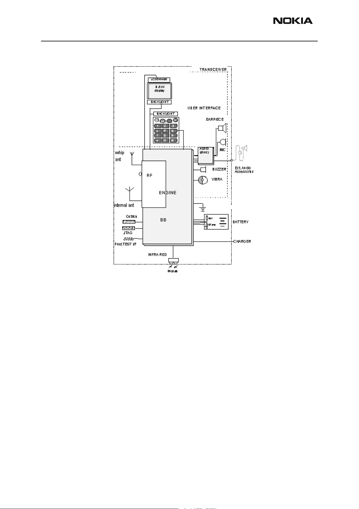
Transceiver NHP-2
Introduction
The NHP-2 is a CDMA DCT 4.0 engine incorporating IS-95B and IS-2000 features with
full 1XRTT data rate capacity. Advanced messaging features include SMS (MO/MT),
Instant Messaging, Nokia ‘Chat’ and Smart Messaging (ring tones, graphics, images, and
animations).
The standard internal battery (BLB-3) provides users with up to four hours of talk time
and 250 hours of standby time.
The transceiver has a full graphic display and the user interface is based on the Jack 3 UI
with two soft keys.
Both an internal and a whip antenna are used. When the whip antenna is in, only the
internal antenna is active. When the whip is retracted, both antennas are active. An
external RF connector also is used.
NHP-2 variants include:
• NHP-2AX (6385) tri-mode;
• NHP-2FX (6370) PCS; and
For additional variant information, refer to Chapter 5, Variants.
Operational Modes
There are several different operational modes: Modes have different states controlled by
the cellular SW. Some examples are: Idle State (on ACCH), Camping (on DCCH), Scanning,
Conversation, No Service Power Save (NSPS) previously OOR = Out of Range.
In the power-off mode, only the circuits needed for power-up are supplied.
In the idle mode, circuits are powered down and only the sleep clock is running.
In the active mode, all the circuits are supplied with power, although some parts might
be in idle state part of the time.
The charge mode is effective in parallel with all previous modes. The charge mode itself
consists of two different states, i.e. the fast charge and the maintenance mode.
The local mode is used for alignment and testing.
Issue 1 05/2002 Nokia Corporation Page 11
Page 12
NHP-2
3. System Module PAMS Technical Documentation
Figure 1: Interconnecting Diagram
Page 12 Nokia Corporation Issue 1 05/2002
Page 13

NHP-2
PAMS Technical Documentation 3. System Module
Engine Module
Environmental Specifications
Normal and extreme voltages
Voltage range:
• nominal battery voltage: 3.6 V
• maximum battery voltage: 4.5 V
• minimum battery voltage: 3.2 V
Temperature Conditions
Temperature range:
• ambient temperature: -30...+ 60o C
• PWB temperature: -30...+85o C
Issue 1 05/2002 Nokia Corporation Page 13
Page 14

NHP-2
V
A
X
3. System Module PAMS Technical Documentation
Baseband Module
The core part of the NHP-2 baseband module consists of two ASICs—UEM and UPP—and
flash memory. The following sections describe these parts.
PA supply
RFIC CTRL
SAFARI
RFCLK
19.44MHz
UPP
MEMADDA
MEMCONT
FLASH
RF Supplies
RF RX/T
BATTERY
UEM
PURX
RF RX/TX
SLEEPCLOCK
32kHz
CBUS/DBUS
UDIO
BB Supplies
KLIGHT/DLIGHT
PWR ON
EXTERNAL AUDIO
BASEBAND
CHARGER CONNECT ION
DCT4 System Connector
UI
IR
EAR
MIC
BUZZER
IBRA
UEM
UEM Introduction
UEM is the Universal Energy Management IC for DCT4 digital handportable phones. In
addition to energy management, it performs all the baseband mixed-signal functions.
Most of UEM pins have 2kV ESD protection. Those signals that are considered to be
exposed more easily to ESD have 8kV protection inside UEM. Such signals are all audio
signals, headset signals, BSI, Btemp, Fbus, and Mbus signals.
Regulators
UEM has six regulators for baseband power supplies and seven regulators for RF power
supplies. VR1 regulator has two outputs VR1a and VR1b. NHP-2 has a DC/DC connector
to provide power to the UPP VCORE.
Bypass capacitor (1uF) is required for each regulator output to ensure stability.
Reference voltages for regulators require external 1uF capacitors. Vref25RF is reference
voltage for VR2 regulator; Vref25BB is reference voltage for VANA, VFLASH1, VFLASH2,
Page 14 Nokia Corporation Issue 1 05/2002
Page 15

NHP-2
PAMS Technical Documentation 3. System Module
VR1 regulators; Vref278 is reference voltage for VR3, VR4, VR5, VR6, VR7 regulators;
VrefRF01 is reference voltage for VIO, VCORE, VSIM regulators, and for RF.
BB RF
VANA: 2.78Vtyp 80mAmax VR1a:4.75V 12mAmax
VR1b:4.75V 12mAmax
Vflash1: 2.78Vtyp 70mAmax
Vflash2: 2.78Vtyp
40mAmax
VSim: 1.8/3.0V 25mAmax VR3:2.78V 20mA
VIO: 1.8Vtyp
150mAmax
Vcore: 1.0-1.8V
200mAmax
VR2:2.78V 100mAmax
VR4: 2.78V 50mAmax
VR5: 2.78V 50mAmax
VR6: 2.78V 50mAmax
VR7: 2.78V 45mAmax
VANA regulator supplies internal and external analog circuitry of BB. It's disabled in
sleep mode.
Vflash1 regulator supplies LCD, IR-module, and digital parts of UEM ASIC. It's enabled
during startup and goes to low Iq-mode in sleep mode.
Vflash2 regulator supplies data cable (DLR-3). It's enabled/disenabled through writing
register and default is off.
VIO regulator supplies both external and internal logic circuitries. It's used by LCD, flash,
Robin, Batman, Bluetooth, and UPP. Regulator goes in to low Iq-mode in sleep mode.
VCORE DC/DC regulator supplies DSP and Core part of UPP. Voltage is programmable and
the startup default is 1.5V. Regulator goes to low Iq-mode in sleep mode.
VR1 regulator uses two LDOs and a charge pump. This regulator is used by Robin RF ASIC
(VR1B) and synthesizer circuits (VR1A).
VR2 is a linear regulator used to supply Robin RF ASIC and the detector circuitry.
VR3 is a linear regulator used by Robin RF ASIC and VCTCXO circuitry.
VR4 is a linear regulator used by the PLL and UHF VCO circuitry.
VR5 is a linear regulator used by the Batman RFIC and the Alfred RF ASIC.
VR6 is a linear regulator used by Robin RF ASIC and TX LO buffer.
Issue 1 05/2002 Nokia Corporation Page 15
Page 16

NHP-2
3. System Module PAMS Technical Documentation
VR7 is a linear regulator used by Batman RF ASIC.
IPA1 and IPA2 are programmable current generators. The 27kW/1%/100ppm external
resistor is used to improve the accuracy of output current. IPA1 is used by lower band PA
and IPA2 is used by higher band PA.
RF Interface
UEM handles the interface between the baseband and the RF section. It provides A/D and
D/A conversion of the in-phase and quadrature receive and transmit signal paths, and
also A/D and D/A conversions of received and transmitted audio signals to and from the
UI section. The UEM supplies the analog AFC signal to the RF section according to the
UPP DSP digital control. It also converts PA temperature into real data for the DSP.
Charging Control
The CHACON block of UEM asics controls charging. Needed functions for charging controls are pwm-controlled battery charging switch, charger-monitoring circuitry, battery
voltage monitoring circuitry and RTC supply circuitry for backup battery charging. In
addition, external components are needed for EMC protection of the charger input to the
baseband module. The DCT4 baseband is designed to electrically support both DCT3 and
DCT4 chargers.
Digital Interface
Data transmission between the UEM and the UPP is implemented using two serial connections, DBUS (9.6 MHz) for DSP and CBUS (1.2 MHz in CDMA) for MCU. UEM is a dualvoltage circuit: the digital parts are running from 1.8V and the analog parts are running
from 2.78V. Vbat (3,6V) voltage regulators inputs also are used.
Audio Codec
The baseband supports two external microphone inputs and one external earphone output. The inputs can be taken from an internal microphone, from a headset microphone,
or from an external microphone signal source through a headset connector. The output
for the internal earpiece is a dual-ended type output, and the differential output is capable of driving 4Vpp to the earpiece with a 60 dB minimum signal to total distortion ratio.
Input and output signal source selection and gain control is performed inside the UEM
ASIC according to control messages from the UPP. Both a buzzer and an external vibra
alert control signals are generated by the UEM with separate PWM outputs.
UI Drivers
There is a single output driver for buzzer, vibra, display, keyboard LEDs, and IR inside
UEM. These generate PWM square wave to devices.
IR Interface
The IR interface is designed into the UEM. The low frequency mode of IR module covers
speeds up to 1.152 mbit/s. The device (Vishay) tranceivers integrate a sensitive receiver
and a built-in power driver. The combination of thin, long resistive and inductive wiring
should be avoided. The inputs (Txd, SD/Mode) and the output (Rxd) should be directly
coupled to I/O circuit. VBAT gives power supply to transmit LED and serial resistor limits
Page 16 Nokia Corporation Issue 1 05/2002
Page 17

NHP-2
PAMS Technical Documentation 3. System Module
current. Receiving infrared data to IR LED, it goes straight to UPP by RXD line. Vflash1 is
the power supply of the IR module transmit.The IR module has one control pin to control
shutdown.
AD Converters
There is an 11-channel analog to digital converter in UEM. The AD converters are calibrated in the production line.
BB-RF Interface Connections
All the signal descriptions and properties in the following tables are valid only for active
signals.
Table 1: PDM Interface
Signal name From To Parameter Min Typ Max Unit Function
RX_IF_AGC UPP
GenIO 9
TX_IF_AGC UPP
GenIO 7
TX_RF_AGC UPP
GenIO 26
PA_GAIN UPP
GenIO 19
Signal
name
From To Parameter Input characteristics Function
Batman Voltage Min
Max
---------------Clk Rate
Robin Vo ltage Min
Max
---------------Clk Rate
Robin Vo ltage Min
Max
---------------Clk Rate
Robin Vo ltage Min
Max
---------------Clk Rate
(1)
0.0
1.75
--------
(1)
0.0
1.75
-------
0.0
1.75
--------
(3)
0.0
1.75
--------
(3)
Table 2: General I/O Interface
1.8
------
9.6
1.8
-------
9.6
1.8
--------
9.6
1.8
--------
9.6
0.1
1.86
-------
19.2
0.1
1.86
--------
19.2
0.1
1.86
--------
19.2
0.1
1.86
--------
19.2
V
-------MHz
V
-------MHz
V
-------MHz
V
-------MHz
Controls gain of VGA r
in receiver
Controls gain of VGA
in IF VGA in Robin
Controls gain of TX
driver in Robin
Controls gain of PA
TX_Gate UPP
Gen IO 8
pullup
PA_Boost UPP
Gen IO 28
pullup
Robin “1” Transmitter Off
“0” Transmitter On
Timing Accuracy
Snapper
Shark
“1” boost mode
“0” data mode
Timing Accuracy
1.38 1.88 V
0 0.4 V
4 chips, and can be up
to a total of 255 chips
1.38 1.88 V
0 0.4 V
4 chips, and can be up
to a total of 255 chips
Punctures the PA’s and
the Robin ASIC
Digital Into RF
Sets PA current for
desired linearity
Digital Into RF
Issue 1 05/2002 Nokia Corporation Page 17
Page 18

NHP-2
3. System Module PAMS Technical Documentation
Table 3: VCTCXO Interface
Signal name From To Parameter Min Typ Max Unit Function
CLK192M_UPP VCTCXO Upp
Batman
Robin
UHF PLL
AFC UEM VCTCXO Voltage Min
Frequency
-----------------------Signal amplitude
Max
------------------------Settling time
Table 4: Regulated Supplies from UEM to RF
Signal
name
VBAT Battery PA & UEM,
VR1A UEM UHF Synth Voltage
From To Parameter Min Typ Max Unit Function
Voltage
external driver
amps
----------------
Current
----------------
Current
(4)
-------
0.5
0.0
2.4
------- -------
3.2
----0
4.6
-----0
3.5
------
4.75
-----4
19.2
-------
1.0
-------
1.5
0.1
2.55
-------
0.2
5.1
-----2A
peak
4.9
-----5
MHz
-------
Vpp
V
------ms
V
------
V
-----mA
High stability clock
signal for logic circuits, AC coupled
sinewave.
Analog Out of RF
Automatic frequency control
signal for VCTCXO
Digital Into RF
Battery supply.
Lower limit is to
guarantee regulator PSRR
Charge pump + linear regulator.
VR1B UEM PA Iref current
sources in
Robin
VR2 UEM Robin driver
amps
VR3 UEM VCTCXO Robin
VHF synthesizer
VR4 UEM UHF VCO, syn-
thesizer
VR5 UEM Batman IF, BB,
LNA, mixer
VR6 UEM Robin IF, BB,
mixers
VR7 UEM Batman VHF
synthesizer
VREFRF01 UEM Batman Vref Voltage 1.334 1.35 1.366 V Voltage Reference
Voltage
----------------
Current
Voltage
----------------
Current
Voltage
----------------
Current
Voltage
----------------
Current
Voltage
----------------
Current
Voltage
----------------
Current
Voltage
----------------
Current
4.6
-----0
2.70
------
2.70
------
2.70
------
2.70
------
2.70
------
2.70
------
4.75
-----4
2.78
------
2.78
------
2.78
------
2.78
------
2.78
------
2.78
------
4.9
-----5
2.86
-----100
2.8
-----20
V
-----mA
V
-----mA
V
-----mA
V
-----mA
V
-----mA
V
-----mA
V
-----mA
Charge pump + linear regulator
Linear regulator
Low noise linear
regulator for
VCTCXO
Low lq linear regulator
Low lq linear regulator
Low lq linear regulator
Low noise linear
regulator for synthesizer
for RF-IC 1.2%
accuracy
Page 18 Nokia Corporation Issue 1 05/2002
Page 19

NHP-2
PAMS Technical Documentation 3. System Module
Table 4: Regulated Supplies from UEM to RF
Signal
name
VREFRF02 UEM Robin Vref Voltage 1.334 1.35 1.366 V Voltage Reference
VIO UEM Digital IO + PLL
From To Parameter Min Typ Max Unit Function
for RF-IC 1.2%
accuracy
digital
Voltage
----------------
Current
1.70
------
1.8 1.88
-----50
V
-----mA
Supply for RF-BB
digital interface
and some digital
parts of RF.
Table 5: Slow A/D Converters
Signal name From To Parameter Min Typ Max Unit Function
PA_TEMP Thermistor UEM Input voltage
range
---------------Input clock freq
PWROUT Robin UEM Input voltage
range
---------------Input clock freq
0
------- ------
0
------- ------
2.741
--------
2.5
2.741
--------
2.5
V
-----MHz
V
-----MHz
PA temperature sensor output voltage
Analog Out of RF
Buffered output of TX
output detector and
TX power supply
Analog Out of RF
FALSE_DET Robin UEM Input voltage
range
---------------Input clock freq
0
------- ------
2.741
--------
2.5
V
-----MHz
protection circuit
that is independent
of main transmitter
on-off control circuit
and minimizes the
possibility of false
transmission caused
by component failure
Table 6: RF-BB Analog Signals
Signal name From To Parameter Min Typ Max Unit Function
RX_IP_RF
RX_IN_RF
RX_QP_RF
RX_QN_RF
TX_IP_RF
TX_IN_RF
TX_QP_RF
TX_QN_RF
Batman UEM Differential volt-
age swing (static)
-------------------------DC level
-------------------------Input Bandwidth
UEM Robin Differential volt-
age swing (static)
--------------------------DC level
---------------------------
-3 dB Bandwidth
1.35
--------
1.3
--------
--------
1.65
-------650
1.4
-------
1.35
-------
0.9
-------
1.7
-------
1.45
--------
1.4
-------615
1.0
-------
1.75
-------1950
Vpp
------V
------kHz
Vpp
------V
------kHz
Differential in-phase
and quadrature RX
baseband signal
Analog Out of RF
Differential quadra-
ture phase TX baseband signal for RF
modulator
Analog into RF
Issue 1 05/2002 Nokia Corporation Page 19
Page 20

NHP-2
3. System Module PAMS Technical Documentation
Table 7: RFIC Control
Signal name From To Parameter Min Typ Max Unit Function
RF_BUS_CLK
RF_BUS_DATA
RF_BUS_EN1X
SYNTH_LE UPP PLL Voltage
UPP Robin/Batman/
PLL
High-level input
voltage, V
Low-level input
voltage, V
High-level output
voltage, V
Low-level output
voltage, V
Clock
Timing reso lu t i on
Table 8: RFIC Control
Signal
name
PURX UEM Robin/Batman Voltage Level
From To Paramete r Min Typ Max Unit Function
------------------------Timing resolution
IH
IL
OH
OL
0
-------- -------
1.8
-------10
2.35
0.5
2.45
0.4
10
V
-----us
V
V
V
V
MHz
V
us
Power Up Reset
for Batman and
Robin
1.2
1.3
01.8
1.3
1.4
9.72
Serial Clock =
Digital Into RF
Bidirectional
Serial Date =
Digital I/O
Latch enable
for Batman and
Robin = Digital
Into RF
Synthesizer
latch enable
UPP
UPP Introduction
NHP-2 uses UPP8Mv2.2 ASIC. The RAM size is 4M. The UPP ASIC is designed to operate
in a DCT4 engine, and is designed as part of the DCT4 common baseband task force. The
DCT4 processor architecture consists of both DSP and MCU processors.
Blocks
UPP is internally partitioned into two main parts: the Brain and the Body.
The Brain consists of the Processor and Memory System (i.e., Processor cores, Mega-cells,
internal memories, peripherals and external memory interface). The following blocks are
included: the DSP Subsystem (DSPSS), the MCU Subsystem (MCUSS), the emulation control EMUCtl, the program/data RAM PDRAM, and the Brain Peripherals–subsystem
(BrainPer).
The Body consists of the NMP custom cellular logic functions. These contain all interfaces and functions needed for interfacing with other DCT4 baseband and RF parts. It
includes the following sub-blocks: MFI, SCU, CTSI, RxModem, AccIF, UIF, Coder, GPRSCip,
BodyIF, SIMIF, PUP and CDMA (Corona).
Page 20 Nokia Corporation Issue 1 05/2002
Page 21

NHP-2
PAMS Technical Documentation 3. System Module
Flash Memory
Introduction
Flash memory is a high-performance, 32-Mbit, single power supply 1.8 Volt-only FLASH
memory device. This device is designed to be programmed in-system with the standard
system 1.8-volt Vcc supply. A 12.0 volt Vpp is not required for program or erase operations, although an acceleration pin is available if faster write performance is required.
The device is a boot-sectored device, consisting of eight 8Kb and 63 sectors of 64Kb
each.
The device has two read modes: asynchronous read and burst mode read. Device powersup in an asynchronous read mode. In the asynchronous mode, the device has two control
functions which must be satisfied in order to obtain data at the outputs. In the linear
mode, the device will deliver a continuous sequential word stream starting at the specified word and continuing until the end of the memory or until the user loads in a new
starting address or stops the burst advance. The burst mode read operation is a synchronous operation tied to the rising edge of the clock. The microprocessor supplies only the
initial address; all subsequent addresses are automatically generated by the device at the
rising edge of subsequent clock cycles. The burst read cycle consists of an address phase
and a corresponding data phase. The device also is capable of Burst Suspend and Burst
Resume operations.
In order to reduce the power consumpition on the bus, a Power Save function is introduced. This reduces the amount of switching on the external bus.
User Interface Hardware
LCD
Introduction
NHP-2 uses black & white GD51 96x65 full dot-matrix graphical display. The LCD module
includes LCD glass, LCD COG-driver, elastomer connector, and a metal frame. LCD module
is included in the light guide assembly module.
Interface
LCD is controlled by UI SW and control signals.
Booster capacitor (C302 1uF) is connected between booster pin (Vout) and ground. The
capacitor stores boosting voltage.
Pin 9 (GND) is the metal frame ground pin, so it is not coming from the display driver.
Keyboard
Introduction
NHP-2 keyboard design is Nokia Jack style, with up and down navigation keys, two soft
keys, 12 number keys, and side volume keys. The PWR key is located on top in IR lens.
Issue 1 05/2002 Nokia Corporation Page 21
Page 22

NHP-2
3. System Module PAMS Technical Documentation
Power Key
All signals for keyboard are coming from UPP asic except pwr key signal which is connected directly to UEM. Pressing of pwr key is detected so that switch of pwr key connects PWONX is of UEM to GND and creates an interrupt.
Keys
Other keys are detected so that when a key is pressed down, the metal dome connects
one S-line and one R-line of UPP to GND and creates an interrupt for SW. Matrix of how
lines are connected and which lines are used for different keys is described in the following table. S-line S0 and R-line R5 are not used.
NC = Not Connected
Lights
Introduction
NHP-2 has 10 LEDs for lighting purposes: six (V304-V309) are for keyboard and four
(V300-V303) for display. LED type is Osram LGM470, green light emitting and SMD
through-hole mounted.
Interfaces
Display lights are controlled by UEM Dlight signal (8-bit register DriverPWMR, bits 3...0).
Dlight output is Pulse Width Modulation (PWM) signal, which is used to control average
current going through LEDs (see the following table) . When battery voltage changes, a
new PWM value is written to the PWM register, which allows the brightness of lights to
remain consistent with all battery voltages. Signal frequency is fixed at 128Hz.
Returns /
Scans
R0 NC Send End NC
R1 Soft left Up Down Soft right
R2 1 4 7 *
R3 2 5 8 0
R4 3 6 9 #
S1 S2 S3 S4
Keyboard lights are controlled by Klight signal from UEM (8-bit register DriverPWMR,
bits 7...4). Klight output is also a PWM signal and is used in a manner similar to Dlight.
Technical Information
Each LED requires a hole in the PWB where the body of the LED is located. Terminals are
soldered on component side of module PWB. LEDs have white plastic body around the
diode itself, which directs the emitted light to UI side. Current for LCD lights is limited by
resistor between Vbatt and LEDs. For keyboard lights, there are resistors in parallel.
Page 22 Nokia Corporation Issue 1 05/2002
Page 23

NHP-2
PAMS Technical Documentation 3. System Module
Vibra
Introduction
Vibra is located on the D-cover and is connected by spring connectors on the PWB. It is
located in the left bottom side of the engine.
Interfaces
Vibra is controlled by pwm signal VIBRA from UEM. This signal allows control of both
frequency and pulse width of signal. Pulse width is used to control current when battery
voltage changes. Frequency control searches for optimum frequency to ensure silent and
efficient vibrating.
Parameter Requirement Unit
Rated DC Voltage 1.3 V
Rated speed 9500 ±3000 rpm
Rated current 11 5 ±20 mA
Starting current 150 ±20 mA
Armature resistant 8.6 ohm
Rated DC voltage available 1.2 to 1.7 V
Starting DC voltage min. 1.2 V
Audio Hardware
Earpiece
Introduction
The 13 mm speaker capsule that is used in DCT3 products also is used in NHP-2.
The speaker is dynamical—very sensitive, and capable of producing relatively high sound
pressure at low frequencies. The speaker capsule and surrounding mechanics comprise
the earpiece.
Microphone
Introduction
The microphone is an electric microphone with omnidirectional polar pattern. It consists
of an electrically polarized membrane and a metal electrode, which form a capacitor. Air
pressure changes (i.e., sound) move the membrane, which causes voltage changes across
the capacitor. Since the capacitance is typically 2 pF, a FET buffer is needed inside the
microphone capsule for the signal generated by the capacitor. The microphone needs
bias voltage as a result of the FET.
Issue 1 05/2002 Nokia Corporation Page 23
Page 24

NHP-2
Ni-MH
GND
Battery
3. System Module PAMS Technical Documentation
Buzzer
Introduction
The functioning principle for the buzzer is magnetic. The diaphragm of the buzzer is
made of magnetic material and is located in a magnetic field created by a permanent
magnet. The winding is not attached to the diaphragm as is the case with the speaker.
The winding is located in the magnetic circuit so that it can alter the magnetic field of
the permanent magnet, thus changing the magnetic force affecting the diaphragm.
This functioning principle makes the buzzer very efficient but also sensitive to external
magnetic fields. It should not be located close to transmitter power wires on PWB. Otherwise, the transmitter current can be heard from the buzzer. The useful frequency range
is approximately 2 kHz-5kHz.
Battery
Phone Battery
Introduction
A 1000 mAh Li-ion battery (BLB-3) is standard in NHP-2.
Interface
The battery block contains NTC and BSI resistors for temperature measurement and battery identification. The BSI fixed resistor value indicates the chemistry and default
capacity of a battery. NTC resistor measures the battery temperature. Temperature and
capacity information is needed for charge control. These resistors are connected to the
BSI and BTEMP pins of battery connector. Phone has pull-up resistors (R202) for these
lines so that they can be read by A/D inputs in the phone (see the following figure).
Resistor array (R206) is ESD protection. There also are spark caps in the BSI and BTEMP
lines to prevent ESD.
UEM
C220
1n
C217
1n
R202/1
100k
R205/1
10k
R205/2
10k
VFLASH 1VANA VBAT
R202/4
100k
C100
10p
connector
VBATT
BSI
BTEMP
OVERCHARGE/
OVERDISCHARG E
PROTECTION
Batteries have a specific red line to indicate if the battery has been subjected to excess
humidity. The batteries are delivered in a "protection" mode, which gives longer storage
time. The voltage seen in the outer terminals is zero (or floating), and the battery is activated by connecting the charger. Battery has internal protection for overvoltage and
overcurrent.
Page 24 Nokia Corporation Issue 1 05/2002
Page 25

NHP-2
1 (+)
2(BSI)
3(BTEMP)
4(GND)
PAMS Technical Documentation 3. System Module
Battery Connector
NHP-2 uses a spring-type battery connector. This makes the phone easier to assemble in
production and ensures a more reliable connection between the battery and PWB.
Signal
#
name
1 VBAT (+) (batt.) VBAT I/O Vbat
2 BSI BSI (batt.) UEM Out Ana.
3 BTEMP BTEMP
4 GND GND GND Gnd
Connected
from - to
(batt.)
Batt. I/O
UEM Out Ana.
Signal properties
A/D--levels--freq./timing
Description /
Notes
Issue 1 05/2002 Nokia Corporation Page 25
Page 26

NHP-2
3. System Module PAMS Technical Documentation
Accessories Interface
System connector (DCT4)
Introduction
NHP-2 uses DCT4 accessories via a DCT4 system connector.
Interface
Interface is supported by DCT4-compatible fully differential 4-wire (XMICN, XMICP,
XEARN, and XEARP) accessories.
Below is a diagram of the DCT4 connector.
GND
VIN
PWMO (GND)
XMICP
XMICN
XEAR
XEARN
HEADINT
MICNMICP
An accessory is detected by the HeadInt- line, which is connected to the XMIC. When
accessory is connected, it generates headint- interruption (UEMINT) to MCU. After that,
hookInt line is used to determine which accessory is connected. This is done by the voltage divider, which consists of a phone's internal pull-up and accessory-specific pulldown. Voltage generated by this divider is then read by the ad- converter of UEM. The
HookInt- interrupt is generated by the button in the headset or by the accessory external
audio input.
The following diagram illustrates accessory detection / external audio.
Page 26 Nokia Corporation Issue 1 05/2002
Page 27

NHP-2
MicGnd
PAMS Technical Documentation 3. System Module
2.7V
Hookint
/MBUS
EAD
HeadintHeadint
MIC1&3 Bias
MIC1P
MIC1N
HF
HFCM
3...25k
UEM
Technical Information
ESD protection is ensured by spark caps, buried capacitor (Z152 and Z154-157), and
inside UEM, which is protected ±8kV. RF and BB noises are prevented by inductors.
PPH-1 Handsfree
Introduction
• provides charging and hand sfree functionality
2.1V
33N
0.8V
33N
1k2
1.8V
0.3V
1k2
Interface
A 4-wire interface is implemented with 2.5mm diameter round plug/jack, which is similar to the “standard” stereo plug, except the innermost contact is split in two.
2. XEARN
4. XEARP
5. HEADINT
3. XMICP
1. XMICN
• built-in speaker
• uses phone microphone, but also has a connector for HFM-8 optional
external microphone (using HFM-8 mutes phone microphone)
Issue 1 05/2002 Nokia Corporation Page 27
Page 28

NHP-2
3. System Module PAMS Technical Documentation
IR module
Introduction
The IR module is used for short-range data transfer. It is a low-power infrared transceiver
module complaint to the IrDA 1.2 standard for fast infrared data communication. The IR
module is located on top of the engine side next to PWR switch.
Interface
IR transmit is controlled by TXD line from UEM.
VBAT gives power supply to transmit LED and serial resistor (R350) limits current. There
also is a filter capacitor (C351) on VBAT-line to ensure proper voltage. Receiving infrared
data from the IR LED, it goes directly to UEM via the RXD line.
VFLASH1 is the power supply of the IR module expects transmit. It is filtered by capacitor
(C350 and C352). The IR module has one control pin to regulate shutdown. Component
V350 is a control-lever-shifter that is used to change proper voltage to IR module from
UPP (GENIO(10) for shutdown.
Technical Information
The IR interface is designed into the UEM. The IR link supports speeds from 9600 bit/s to
1.152 MBit/s, up to 1m. A special baud rate is used for the NMP-specific speech and
control information transmission. This dedicated protocol has special HW support for
extracting the audio and control information.
IRModuleFIR-pin can be set: ’0’ = slow up to 115 kbps. Another way to set module speed
SIR or MIR is to use TXD/SD SW control; then NC-pin is unconnected.
This module needs one 2.7V_logic control output from digi-ASIC. TFDU5102 has split
power supply and RXD is tristate at shutdown.
Charger IF
Introduction
The charger connection is implemented through the bottom connector. DCT-4 bottom
connector supports charging with both plug chargers and desktop stand chargers.
There are three signals for charging. Charger gnd pin is used for both desktop and for
plug chargers as well as charger voltage. PWM control line, which is needed for 3-wire
chargers, is connected directly to gnd in module PWB so the NHP-2 engine doesn't provide any PWM control to chargers. Charging controlling is done inside UEM by switching
UEM internal charger switch on/off.
Interface
The fuse F100 protects phone from too high currents (e.g., when broken or pirate chargers are used). L100 protects engine from RF noises, which may occur in charging cable.
V100 protects UEM ASIC from reverse polarity charging voltage and from too high
Page 28 Nokia Corporation Issue 1 05/2002
Page 29

NHP-2
PAMS Technical Documentation 3. System Module
charging voltage. C105 is also used for ESD and EMC protection. Spark gaps are used for
ESD protection right after the charger plug.
Issue 1 05/2002 Nokia Corporation Page 29
Page 30

NHP-2
X
3. System Module PAMS Technical Documentation
Test Interfaces
Production Test Pattern
Interface for NHP-2 production testing is 5-pin pad layout in BB area (see figure below).
Production tester connects to these pads by using spring connectors. Interface includes
MBUS, USRX, FBUSTX, VPP, and GND signals. Pad size is 1.7mm. The same pads also are
used for AS test equipment such as module jig and service cable.
Other Test Points
BB ASICs and flash memory are CSP components and the visibility to BB signals is very
poor. This makes measuring of most of the BB signals impossible. In order to debug BB at
least at some level, the most important signals can be accessed from 0.6mm test points.
The figure below shows test points located between UEM and UPP. There is an opening in
baseband shield to provide access to these pads.
2.
FBUS_TX
6.
VPP
3.
FBUS_R X
8.
7.
MBUS
UEM (D200)
GND
EMC
General
EMC performance of the NHP-2 baseband is improved by using a shield to cover main
J414
DBUSCLKDBUSDA
J403
J413
J402
PURXSLEEPX
SLEEPCLK
J404
J405
UEMINT
CBUSDA
J407
J415
DBUSEN1X
UPP (D400)
CBUSENX
J408
J412
FBUSRX
CBUSCLK
J406
J409
MBUSTX MBUSR
FBUSTX
J411
J410
Page 30 Nokia Corporation Issue 1 05/2002
Page 31

NHP-2
PAMS Technical Documentation 3. System Module
components of BB, such as UEM, UPP, and Flash. UEM has internal protection against
±8kV ESD pulse. BB shield is soldered into PWB and it also increases the rigidity of PWB
in BB area, thus improving phone reliability. Shield also improves thermal dissipation by
spreading the heat more widely.
A protective metal deck is located underneath the battery and is grounded to both the
BB shield and the RF shield.
BB Component and Control I/O Line Protection
Keyboard Lines
ESD protection for keyboard signals is implemented by using metaldome detection.
Grounded keydomes are very effective for ESD protection and do not require additional
components for ESD protection -> very low cost solution. The distance from A-cover to
PWB is made longer with the spikes in the keymat. C-cover metallization also protects
keyboard lines.
C-Cover
C-cover on UI side is metallized from inner surface (partly) and grounded to module gnd.
All those areas where plated C-cover touches PWB surface are grounded and solder mask
are opened.
PWB
All edges are grounded from both sides of PWB and solder mask is opened from these
areas. Target is that any ESD pulse faces ground area when entering the phone (e.g.,
between mechanics covers).
All holes in PWB are grounded and plated through holes (with the exception of LED
holes, which cannot be grounded).
LCD
ESD protection for LCD is implemented by connecting metal frame of LCD to gnd. Connection is only on one side, at the top of the LCD, and that is not the best solution. Due
to SAR issues, the C-cover metallization is cut in the middle, just under the display, making the whole engine more sensitive to ESD. Software protects against LCD crashing.
Microphone
Microphones metal cover is connected to gnd and there are spark gaps on PWB. Microphone is an unsymmetrical circuit, which makes it well protected against EMC.
EARP
EARP is protected with the C-cover metallization and with plastic-fronted earpiece.
Buzzer
PWB openings with C-cover metallization protect buzzer from ESD.
Issue 1 05/2002 Nokia Corporation Page 31
Page 32

NHP-2
3. System Module PAMS Technical Documentation
IRDA
PWB openings with C-cover metallization protect IRDA lines from ESD.
Bottom Connector Lines
HF and HFCM lines have spark gaps, ferrite bead RF filter (450W/100MHz), and PWB
capacitors (5x5mm).
Headint and Hookint have spark gaps as well as RC-circuit (1k & 1n).
Charger + is protected with a ferrite bead (42W/100MHz) and capacitor to ground (1n).
Charger - is protected with a ferrite bead (42W/100MHz) and PWB capacitor (5x5mm)
separating it from the battery ground.
Battery Connector Lines
BSI and BTEMP lines are protected with spark gaps and RC circuit (10k & 1n) where resistors are size 0603.
M-bus F-bus
Opening in the protective metal deck underneath battery is so small that ESD does not
get into M-bus and F-bus lines in the production test pattern.
Page 32 Nokia Corporation Issue 1 05/2002
Page 33

NHP-2
PAMS Technical Documentation 3. System Module
General Information About Testing
Phone operating modes
Phone has three different modes for testing/repairing phone. Modes can be selected with
suitable resistors connected to BSI- and BTEMP- lines as follows:
Mode BSI- resistor BTEMP- resistor Remarks
Normal 68k 47k
Local 560_ (<1k_) What ever
Test > 1k 560_ (<1k_) Recommended with base-
band testing. Same as
local mode, but making a
phone call is possible.
The MCU software enters automatically to local or test mode at start-up if corresponding resistors are connected.
Note! Baseband doesn't wake up automatically when the battery voltage is connected (normal mode).
Power can be switched on by
• pressing the PWR key
• connectin g a charger
• RC-alarm function
In the local and test mode, the baseband can be controlled through MBUS or FBUS (FBUS
is recommended) connections by Phoenix service software.
RF Module
Requirements
The NHP-2FX RF module supports CDMA1900 as described in:
• J-STD-018 Recommended Minimum Performance Requirements for 1.8 to 2.0 GHZ
Code Division Multiple Access (CDMA) Personal Stations;
• IS2000-2-A Physical Layer Standard for cdma2000 Spread Spectrum Systems; and
• IS-98D (Draft 4) Recommended Minimum Performance Standard for Spread Spectrum
Mobile Stations.
Temperature Conditions
Surface temperature (SPR5 - Product Safety)
Issue 1 05/2002 Nokia Corporation Page 33
Page 34

NHP-2
3. System Module PAMS Technical Documentation
Maximum temperature rise is 50o C for nonmetallic surfaces and 30o C for metal surfaces at room temperature.
Other temperature requirements (SPR4 - Operating Conditions)
o
Meeting requirements: -30...+ 60
Storage requirements: -30...+85o C
C
Main Technical Characteristics
Environmental Specifications
Normal and extreme voltages
Voltage range:
• nominal battery voltage: 3.6 V
• maximum battery voltage: 4.5 V
• minimum battery voltage: 3.2 V
Temperature conditions:
• ambient temperature: -30...+ 60o C
• PWB temperature: -30...+85o C
• storage temperature range: -40 to +85o C
Antenna
A dual-band, whip antenna/internal antenna combination is used.
Page 34 Nokia Corporation Issue 1 05/2002
Page 35

NHP-2
PAMS Technical Documentation 3. System Module
Transmitter
WHIP
ANT.
Internal
ANT.
RX
RF
Conn.
PCS DUPLEXER
Isolator
SNAPPER
PA
SPLIT BAND
SAW FILTER
Hi BAND
Lo BAND
Detector
HORNET
TX_RF_AGC
( UPP )
P_DET
P_REF
Figure 2: PCS block diagram
PCS
DVR
CELL
DVR
UHF LO
ROBIN
UP CONV
Current Mirror
PA_AGC
( UPP )
IF AGC
PWROUT
(UEM)
19.2
MHz
CLK
VHF PLL
TX_ IF_AGC
( UPP )
DATA
SIO
Enable
Resonator
CLK
Filter &
VHF SYNTH
Div By 2
I/Q
MODBBFilter
2
I
inputs
Q
2
Figure 3: Trimode block diagram
The transmit chain up to the RF driver stage is integrated into one transmit-integrated
circuit called Robin, with external power amplifiers (PA). The channel bandwidth is 50
kHz.
All data transmitted on the channel is convolutionally encoded and block-interleaved.
Modulation is 64-ary orthogonal (RC1 and RC2) and direct sequence spread by a quadrature pair of PN sequences at a fixed chip rate. The data is filtered, O-QPSK modulated
and up-converted to the appropriate transmission frequency. RC3 and RC4 use HPSK
Issue 1 05/2002 Nokia Corporation Page 35
Page 36

NHP-2
3. System Module PAMS Technical Documentation
modulation at data rates up to 153.6 kBPS (RC3) and 115.2 kBPS (RC4).
The baseband I/Q signals are converted to IF frequency in the I/Q modulator by Quadrature mixing. The modulated IF signals go through a variable gain amplifier (IF AGC) and
then are routed either to the PCS TX path. The path consists of an upconverter and a
variable gain RF amplifier. The IF signal is converted up to RF with a differential output
upconverter and then fed to the RF amplifier. The RF amplifier has variable gain capability (RF AGC) with up to 25 dB of dynamic gain control.
The outputs of the RF amplifiers are differential. The differential outputs from Robin are
combined into single-ended output by an external balun and fed into an external driver
amplifier module (Hornet for PCS and Tomcat for cell). There are two outputs from this
module that feed a split-band filter. The split-band filter output is connected to a SPDT
RF switch that results in a single output.
This split-band filter provides the needed Rx band rejection performance. The wide PCS
Tx band (60 MHz) and small separation (20 MHz) between TX and Rx band prevents a
single SAW filter from achieving the required Rx rejection. As a result, the PCS band SAW
filter is divided into two bands, each 35 MHz wide.
The output of the SPDT RF switch then is connected to the PA (Snapper). Out of the PA is
an isolator, then antenna.
The PA modules contain all the necessary matching networks and reference current circuitry for variable gain control and biasing ON/OFF. A variable reference current is used
to vary the PA gain and PA bias current. The variable gain technique reduces PA current
consumption and improves the signal-to-noise ratio at low output power levels. The precision bias current (and gain) control is achieved by varying the PA reference current
with a PDM control voltage. The PA module also incorporates a “Boost” mode that can be
turned on for signal modulations exhibiting Peak to Average (PAR) ratios greater than
4.0.
The transmitter chain utilizes smart power techniques and only the required circuits are
powered at the appropriate times. In order to save energy in puncture mode, when there
is no speech activity during a call, the driver and power amplifiers and the Robin IC are
switched ON and OFF rapidly. These units also are in the OFF state when the transmitter
is in standby. The ON/OFF switch commands are issued by a Digital ASIC (UPP). The UPP’s
PDM controls a current mirror in Robin that provides the PA reference current. Switching
each reference current ON/OFF switches each PA ON/OFF. The VHF synthesizer and power
detector circuits are left on during the puncture mode.
Page 36 Nokia Corporation Issue 1 05/2002
Page 37

NHP-2
PAMS Technical Documentation 3. System Module
Synthesizer
Refer to Figure 2 for a block diagram that illustrates all three synthesizers and how they
interconnect in the system.
Batman
RX VHF Synthesizer
128PCS
UHF Synthesizer
Phase
Detector
9-Bit B
Counter
53PCS
LMX2377
Phase
Detector
13-Bit B
Counter
1286 - 1323PCS
Prescaler
32/33
5-Bit A
Counter
Prescaler
5-Bit A
Counter
0 - 31
Charge
Pump
2 mA
12PCS
Charge
Pump
4 mA384PCS
32/33
VCO Band
Control
RX VHF VCO
Tank
UHF VCO
Splitter
UHF LO
Alfred
RF_BUS_CLK
RF_BUS_DATA
RF_BUS_EN1X
SYNTH_LE
Reference
Divider
Reference
Divider
AFC
UEM
VCTCXO
19.2 MHz
UHF LO Synthesizer
The UHF LO synthesizer generates the first RX LO frequency for the receiver (down-conversion) and the second TX LO frequency for the transmitter (up-conversion). The synthesizer is a dual-modulus prescaler type and utilizes a phase-frequency detector with a
charge pump that sinks or sources currents, depending upon the phase difference
between the phase detector input signals.
ROBIN
SSB
Mixers
TX VHF Synthesizer
384
PCS
Phase
Detector
9-Bit B
Counter
260
Prescaler
5-Bit A
Counter
PCS
Charge
Pump
2 mA
32/33
VCO
4
Band
Control
Reference
Divider
PCS
UPP
Figure 4: Synthesizer System Block Diagram
TX VHF VCO
Tank
Issue 1 05/2002 Nokia Corporation Page 37
Page 38

NHP-2
3. System Module PAMS Technical Documentation
For PCS, channel spacing and the comparison frequency is 50 kHz. For the cellular AMPS/
CDMA band, channel spacing is 30 kHz. An external buffer is provided for high isolation
between Robin and the VCO to reduce VCO pulling due to changing load.
1st TX VHF LO Synthesizer (Robin)
The TX VHF Synthesizer is integrated within the Robin RFIC and generates the LO signals
for the IQ-modulator in Robin. The synthesizer has an internal VCO with an external resonator. The VCO operates at two times the CELL and PCS IF frequencies. A band-switch
signal, VCO_Band, is used to shift the center frequency of the external resonator.
The synthesizer is a dual-modulus prescaler type, and utilizes a phase detector with a
charge pump that sinks or sources currents, depending on the phase difference between
the detector input signals. The width of the pulses depends on the phase difference
between the signals at input of the phase detector. The main divider, auxiliary divider,
and reference divider are programmable through the serial interface to Robin.
The TX VHF Synthesizer generates 346.2 MHz for Cell Band and 416.2 MHz for PCS band.
The TX VHF Synthesizer comparison frequency for Cell Band is 30 kHz and PCS band is 50
kHz.
2nd RX VHF LO Synthesizer (Batman)
The RX VHF Synthesizer is integrated within the Batman RFIC and generates the LO signals for the IQ demodulator in Batman. The synthesizer has an internal VCO with an
external resonator. The VCO operates at two times the common 128.1 MHz RX IF frequency. A band-switch signal, Band_Sel, is used to select the band of operation for the
UHF VCO.
The synthesizer is a dual-modulus prescaler type, and utilizes a phase detector with a
charge pump that signals or sources currents, depending upon the phase difference
between the detector input signals. The width of the pulses depends on the phase difference between the signals at input of the phase detector. The main divider, auxiliary
divider, and reference divider are programmable through the serial interface to Batman.
The RX VHF Synthesizer generates 256.2 MHz for both Cell Band and the PCS Band.
The RX VHF Synthesizer comparison frequency for both Cell Band and PCS Band is 160
kHz.
VCTCXO - System Reference Oscillator
The VCTCXO provides the frequency reference for all the synthesizers. It is a voltage-controlled, temperature-compensated, 19.2MHz crystal oscillator that can be pulled over a
small range of its output frequency. This allows for an AFC function to be implemented
for any frequency accuracy requirements. This is done by DSP processing of received I/Q
signals.
Closed loop AFC operation allows very close frequency tracking of the base station to be
done in CDMA mode. This will enable the unit to track out aging effects and give the
Page 38 Nokia Corporation Issue 1 05/2002
Page 39

NHP-2
PAMS Technical Documentation 3. System Module
required center frequency accuracy in cellular and PCS bands.
The most practical way of clock distribution is driving all three chips (UHF PLL, Batman,
and Robin) directly from the VCTCXO. A buffer is used to drive the UPP in order to isolate
the UPP’s digital noise from the VCTCXO, which prevents contamination of the 19.2 MHz
reference onto the PLL chips of the system. Since the VCTCXO output is a sinewave, such
clock distribution will not cause any clock signal integrity problems, even for relatively
long traces (what might occur in case of a digital square waveform with fast transition
times). The VCTCXO output is AC, coupled to Batman, Robin, UFH PLL, and the digital
ASICs (see Figure 3) to eliminate DC incompatibility between those pins.
Figure 5: VCTCXO Clock Distribution
Receiver
IQ
PCS
PCS
LNA
UHF
VCO
Cell
LNA
RFA
LOA
Cell
RFA
ALFRED
AMPS
CDMA
IF
128.1MHz
CDMA
IF SAW
VGA
DEMOD
BBFIL/BBAMP
BATMAN D
Figure 6: Columbia Receiver Block Diagram
The receiver is a dual conversion I/Q receiver with a first IF of 128.1 MHz. The front-end
Issue 1 05/2002 Nokia Corporation Page 39
ADC
I
Q
Page 40

NHP-2
3. System Module PAMS Technical Documentation
RFIC (Alfred) contains a low noise amplifier (LNA), a radio frequency amplifier (RFA), a
down-converter, an intermediate frequency amplifier (IFA), and a local oscillator amplifier (LOA). This IC also contains 800 MHz blocks, but these are not active in this application. Between the LNA and the RFA is a bandpass filter which will reject out-of-band
spurious and act as image rejection. The IF filter is between the Alfred IC and the BatmanD IC. The purpose of this filter is to guarantee rejection in adjacent and alternate
channels.
The RX IF ASIC BatmanD is used to convert the IF down to baseband I and Q. The ASIC
contains a VGA section, IQ demodulator, baseband filters (BBFIL) for AMPS and CDMA.
Switchable gain baseband amplifier (BBAMP), and RX VHF PLL. The I/Q BB signals are
output to UEM chip for analog-to-digital conversion and further signal processing.
Page 40 Nokia Corporation Issue 1 05/2002
 Loading...