

Page 1

Programmes After Market Services
NHP-2 Series Transceivers
9. Troubleshooting
Issue 1 05/2002 Nokia Corporation
Page 2

NHP-2
9. Troubleshooting PAMS Technical Documentation
Page 2 Nokia Corporation Issue 1 05/2002
Page 3

NHP-2
PAMS Technical Documentation 9. Troubleshooting
Contents
Page No
Transceiver Troubleshooting ......................................................................................... 5
Baseband Description ..................................................................................................5
BB and RF Architecture............................................................................................ 6
Power Up and Reset.................................................................................................. 6
Troubleshooting ........................................................................................................ 8
Phone is totally dead ............................................................................................... 11
Phone Doesn’t Stay On or Phone is Jammed.......................................................... 12
Flash programming ................................................................................................. 14
Flash programming ................................................................................................ 18
Charging Operation................................................................................................. 19
Charger troubleshooting.......................................................................................... 22
Display and Keyboard............................................................................................. 23
Display faults........................................................................................................... 24
Keypad faults........................................................................................................... 27
Audio....................................................................................................................... 29
Accessories.............................................................................................................. 30
Audio Troubleshooting ........................................................................................... 31
Microphone failure.................................................................................................. 32
Vibra failure ............................................................................................................ 33
Buzzer failure.......................................................................................................... 34
Receiver fault finding ................................................................................................35
General instructions for RX troubleshooting.......................................................... 35
Path of the received signal ...................................................................................... 35
Fault finding charts for receiver chain .................................................................... 36
Cell CDMA............................................................................................................. 39
Troubleshooting 128.1 MHz IF Saw Filter............................................................. 39
PCS.......................................................................................................................... 39
Transmitter fault finding ............................................................................................43
General instructions for TX troubleshooting .......................................................... 43
Path of the transmitted signall................................................................................. 43
Fault finding charts for transmitter.......................................................................... 44
AMPS...................................................................................................................... 44
Cell CDMA............................................................................................................. 46
PCS (only dualbander)............................................................................................ 47
Synthesizer fault finding ............................................................................................51
19.2 MHz reference oscillator................................................................................. 51
Fault finding chart for 19.2 MHz oscillator ............................................................ 52
RX VHF VCO......................................................................................................... 52
Fault finding chart for RX VHF VCO .................................................................... 53
TX VHF Synth........................................................................................................ 53
Fault finding chart for TX VHF VCO..................................................................... 54
UHF Synthesizer..................................................................................................... 54
Fault finding chart for UHF Synthesizer ................................................................ 55
Test Point Diagrams................................................................................................ 56
Issue 1 05/2002 Nokia Corporation Page 3
Page 4

NHP-2
9. Troubleshooting PAMS Te chnical Documentation
Page 4 Nokia Corporation Issue 1 05/2002
Page 5

NHP-2
PAMS Technical Documentation 9. Troubleshooting
Transceiver Troubleshooting
Baseband Description
The baseband module is a CDMA dual-band engine. Baseband architecture is based on
the DCT4 Apollo engine. The baseband consists of three new ASICs: Universal Energy
Management (UEM), Universal Phone Processor (UPP), and Flash 64 Megabit.
The baseband architecture supports a power-saving function called “sleep mode”. This
sleep mode shuts off the VCTCXO, which is used as a system clock source for both RF and
Baseband. During the sleep mode, the system runs from a 32 kHz crystal. The phone is
wakened by a timer running from this 32 kHz clock supply. The sleep time is determined
by network parameters. Sleep mode is entered when both the MCU and the DSP are in
standby mode and the normal VCTCXO clock is switched off.
NHP-2 supports both three- and two-wire types of DCT3 chargers. There is a separate
PWM output for controlling the three-wire charger. Charging is controlled by the UEM
ASIC and by EM SW running in the UPP.
Issue 1 05/2002 Nokia Corporation Page 5
Page 6
NHP-2
9. Troubleshooting PAMS Te chnical Documentation
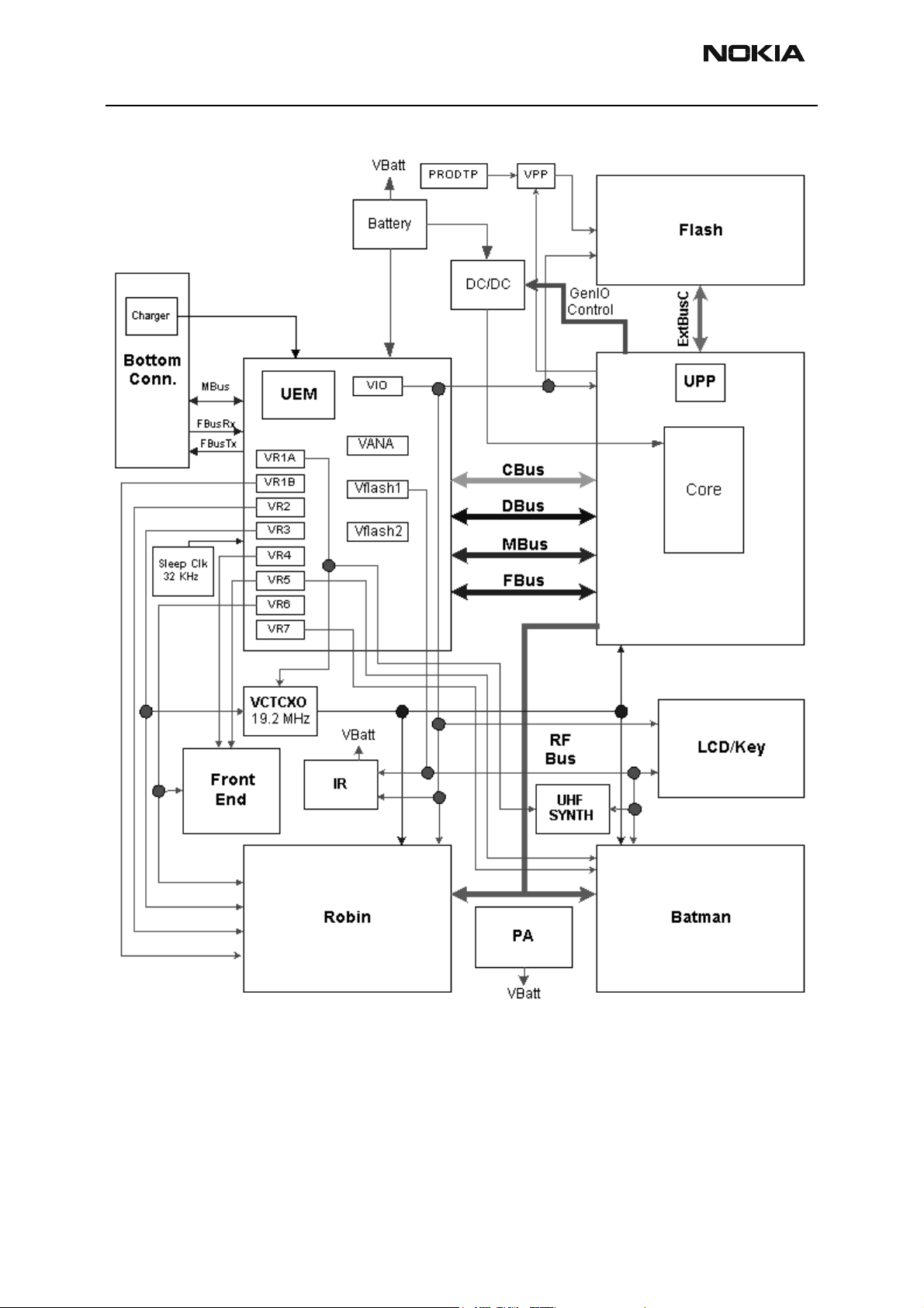
BB and RF Architecture
Figure 1: NHP-2 Power Distribution
Power Up and Reset
Power up and reset is controlled by the UEM ASIC. There are three ways to power up the
baseband module:
1 Power Button (grounding the PWRONX pin of the UEM).
Page 6 Nokia Corporation Issue 1 05/2002
Page 7
NHP-2
PAMS Technical Documentation 9. Troubleshooting
2 Connect the charger to the charger input.
3 RTC Alarm (when the RTC logic has been programmed to give an alarm).
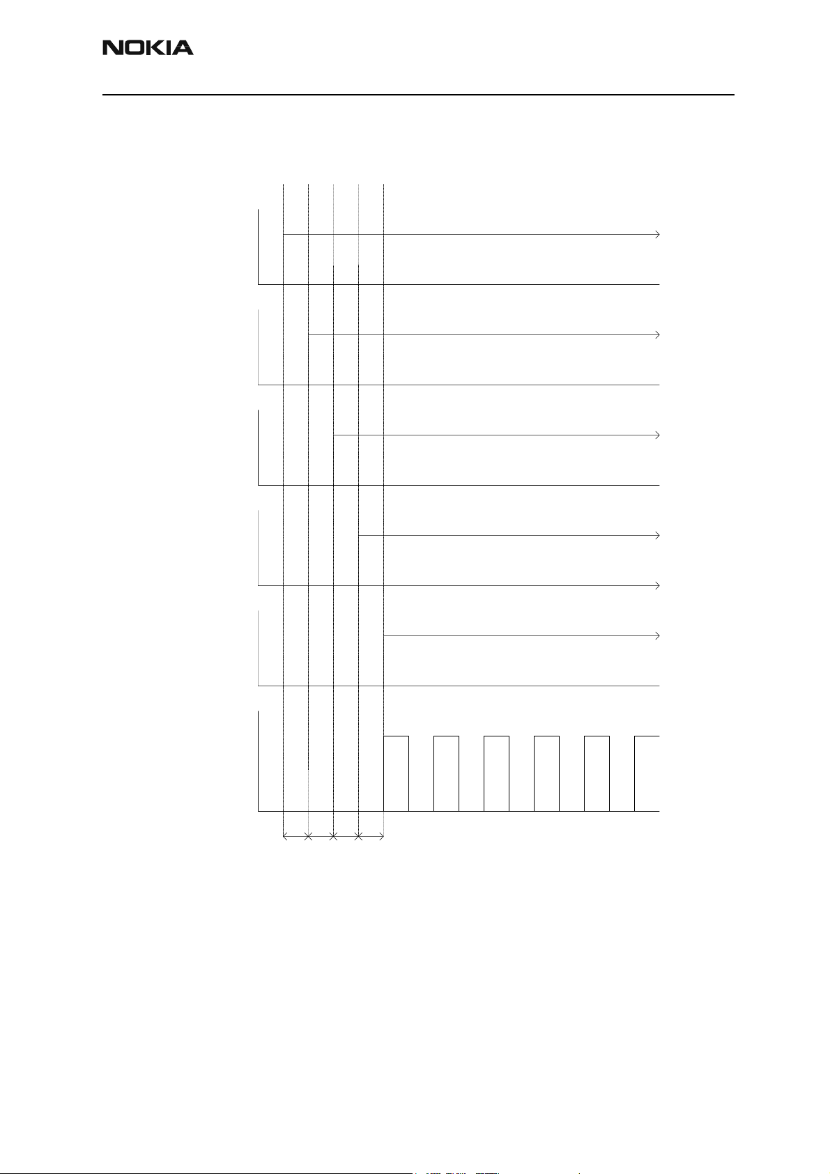
Reference signal
PwrOnX
Charger Detection
RTC
UEMRSTX
VFlash1
VIO
VCORE
VANA
VR3
19.2MHz Clk
PURX
32kHz XTAL
t1 t2 t4t3
t1 = 20ms
t2 = 200ms
t3 = 500us
t4 = 20ms
Figure 2: UEM start-up sequence from reset to power-on mode
Issue 1 05/2002 Nokia Corporation Page 7
Page 8
NHP-2
9. Troubleshooting PAMS Te chnical Documentation
Troubleshooting
First, carry out a thorough visual check of the module. Make sure that:
- there are no mechanical damages
- solder joints are OK
Before changing anything, ALL SUPPLY VOLTAGES AND SYSTEM CLOCK / SLEEP CLOCK
should be checked.
Power up faults
Power-up sequence
UEM acts as a HW master during start up
1 VBATT limits: 2.1V for internal state machine, 3V triggering whole startup
2 Regulator sequencing
• Hw "core" regulators "on": VANA, VIO, VFLA SH1, VFLASH2, and
VCORE, which provide nominal voltages and curre nts according to
Table 1.
Page 8 Nokia Corporation Issue 1 05/2002
Page 9
NHP-2
PAMS Technical Documentation 9. Troubleshooting
Table 1: Baseband regulators
Maximum
Regulator
VCORE (dc/dc) 300 1.5 Output voltage selectable 1.0V/1.3V/1.5V/1.8V.
VIO 150 1.8 Always enabled, except during power-off mode.
VFLASH1 70 2.78 Always enabled, except during power-off mode.
VFLASH2 40 2.78 Enabled only when data cable is connected.
VANA 80 2.78 Enabled only when the system is awake. (Off
current
(mA)
Vout (V) Notes
Power-up default: 1.5V
during sleep mode and power-off mode.)
• UEM supplies voltages VR1A, VR1B, VR2, VR3, VR4, VR5, VR6,
and VR7 for RF. See Table 2.
Table 2: RF regulators
Maximum
Regulator
VR1A 10 4.75 Enabled when receiver is on.
VR1B 10 4.75 Enabled when transmitter is on
VR2 100 2.78 Enabled when transmitter is on
VR3 20 2.78 Enabled when SleepX is high
VR4 50 2.78 Enabled when receiver is on
VR5 50 2.78 Enabled when receiver is on
VR6 50 2.78 Enabled when transmitter is on
VR7 45 2.78 Enabled when receiver is on
current
(mA)
Vout (V) Notes
3 Reset releasing delay
• Supply voltages stabilize to their UEM hw default value
• RFCLK grows to full swing
• Core is ready to run but waiting for PURX release
4 Reset releasing
• UPP releases the SLEEPX up to "non sleep" -state to prevent the
UEM switching the regulators "OFF"
Issue 1 05/2002 Nokia Corporation Page 9
Page 10

NHP-2
9. Troubleshooting PAMS Te chnical Documentation
5 MCU starts running the Bootsrap Code
• written in stone/ UPP internal ROM
• the program checks if there exists any reason for FDL mode (Flash
Down Load)
• If there exists executable code in FLASH and there exists no reason
for FDL, the MCU starts running the MCU pro gram from FLASH.
6 MCU runs the FLASH MCU code the phone initialization, user interfaces, internal
blocks, etc.
• Core regulator voltage setting for required DSP speed
• Initializes the DSP and concerning hw
Releases DSP reset -> DSP starts running
1 Power key pressed
• After 20ms, UEM enters RESET MODE if VBAT>Vmstr+
• VFLASH1, Vana, Vcore, Vio, and VR3 goes high.
• VCTCXO enabled by VR3 -> RFClk 19.44 MHz running.
2 Purx released
• Purx released by UE M , U EM IN T go es high for 100 ms , Sle epX goes
high and SleepClk (32 KHz) starts running.
3 Software running
• Default value of V core is 1.5 V.
• Cbus (1.2MHz) and Dbus (9.6MHz) clocks start running.
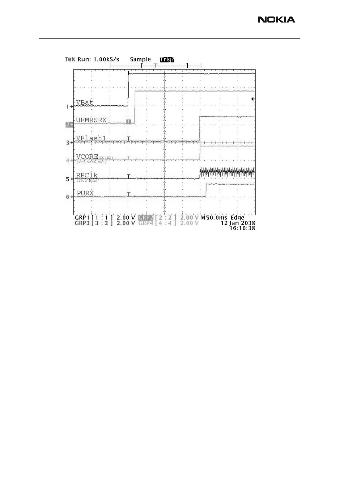
Note! In case of power up faults, it's not possible to force phone on by disabling watchdog. Instead it's
recommended to use normal or single triggering on oscilloscope, so that it's possible to see if signal
goes to its normal value even for a while when power key is pressed.
Page 10 Nokia Corporation Issue 1 05/2002
Page 11
NHP-2
PAMS Technical Documentation 9. Troubleshooting
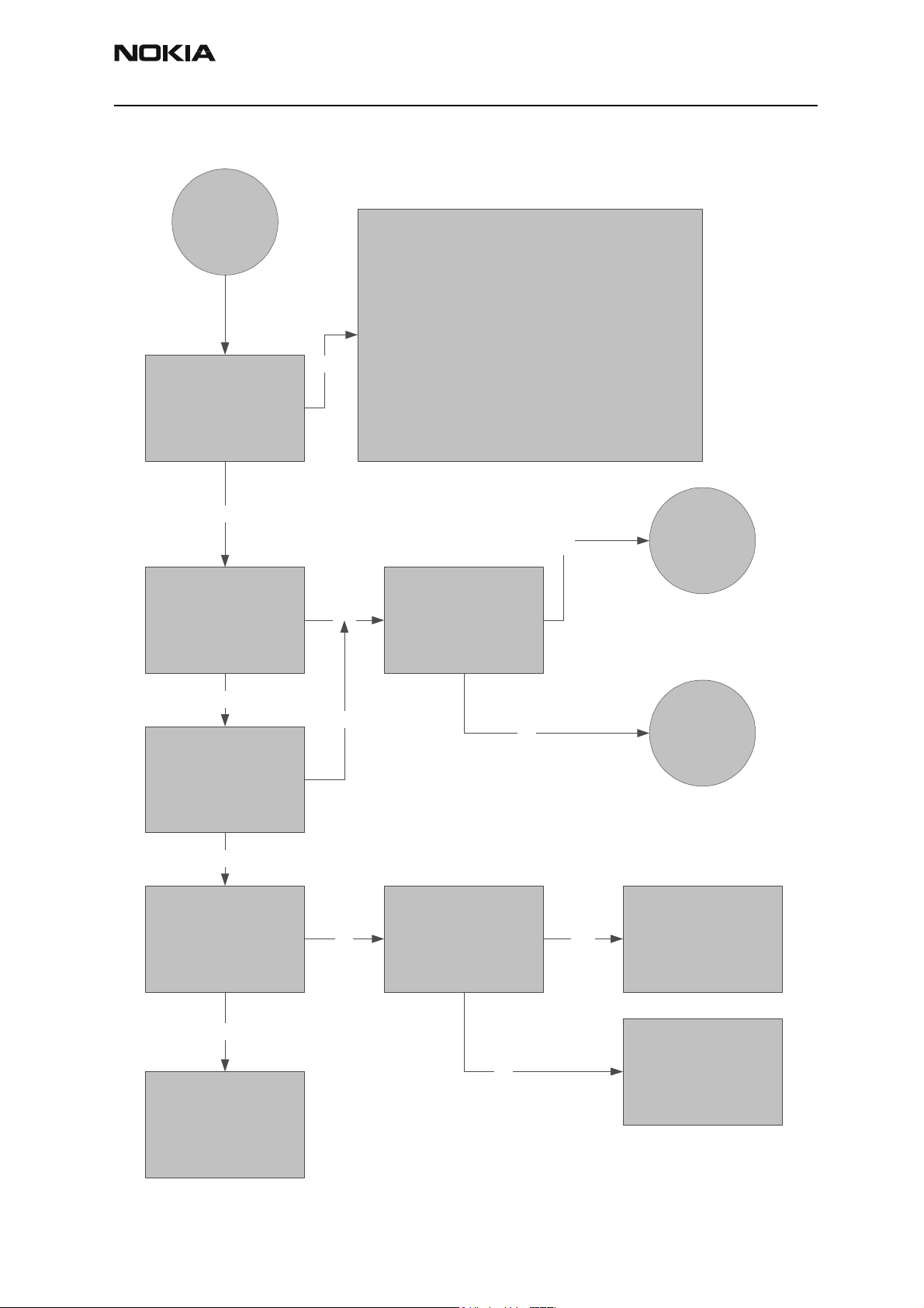
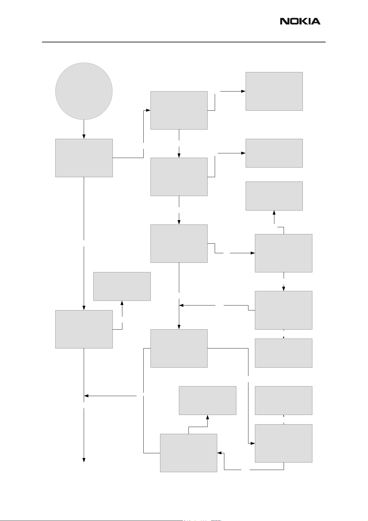
Phone is totally dead
Phone is dead
-If current is zero, check X101 solder and VBATT lines
-If current is too high, check for shorts
-Make sure all BB regulators are at their respective
voltage levels (e.g. , VANA, VIO, VCORE (DC-DC),
VFlash1, and VR3. See phone's top view diagram for
Yes
Phone current is zero
or too high?
test points
-Make sure the System Clk is 19.2 MHz and that the
Sleep Clk is 32 KHz
-Make sure PURX and SleepX signals are high (1.8V)
No
Phone current is < 30 mA
No
Phone current is <= 35 mA
Yes
Is phone in Local Mode?
Yes
No
Is phone flash programming
OK?
No
Check BSI line X101, R202,
R206, C230, C109.
Are they OK?
Yes
Phone is
jammed
Flash faults
YesNo
Change UEM
Yes
No
OK restart
Repair
Issue 1 05/2002 Nokia Corporation Page 11
Page 12
NHP-2
9. Troubleshooting PAMS Te chnical Documentation
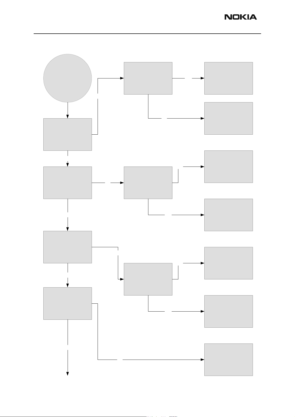
Phone Doesn’t Stay On or Phone is Jammed
Check VBATT, VIO,
Phone is jammed
No
VCORE, VFlash1, VANA,
VR3 capacitors.
Are they OK? (See phone
top view diagram for
capacitor locations).
Yes
Check RSI/BTEMP lines
and VBATT lines.
If OK, change UEM.
Measure VIO, VCORE,
Vflash1, VANA, and VR3
voltages.
Are they OK?
Yes
Measure 32kHz Sleep Clk
from test point.
Is it OK?
Measure 19.2MHz RF Clk
at test point J499.
Is it OK?
Yes
No
Measure 32kHz Clk crystal.
Is it OK?
No
Measure 19.2 MHz Clk
coming from VCTCXO at
C524.
Is it OK?
No
Repair
No
YesYes
No
Change B200
Change UEM
Check G503, C505, C520,
C502, C523, C525, C524,
R511, R510, R512, R520,
R521, R522, R517, R516.
If OK, change G501.
Measure PURX and SleepX
at test points J402 and
J403.
Are they high (1.8V)?
Yes
Yes
No
Change UPP
Change UEM
Page 12 Nokia Corporation Issue 1 05/2002
Page 13

NHP-2
PAMS Technical Documentation 9. Troubleshooting
Phone shuts down after
32 seconds
No
Measure DBusClk 9.6MHz
signal from test point J413.
Is it OK?
Yes
Read phone info.
Is it OK?
No
No
Has the phone been
flashed?
Yes
Measure watchdog signal
CBusDA from test point
J407.
Is it OK?
Change UPP
Yes
Measure FBusRx signal
during phone info read from
test point J412.
Is it OK?
No
NoYes
No
Flash the phone
Change UPP and re-flash
Change UEM and re-flash
Change UEM
Yes
Yes
Measure FBusTx signal
during phone info read from
test point J411.
Retest
Is it OK?
No
Yes
Change UPP
Change UEM
Issue 1 05/2002 Nokia Corporation Page 13
Page 14

NHP-2
9. Troubleshooting PAMS Te chnical Documentation
Flash programming
Connections to Baseband
The flash programming equipment is connected to the baseband using test pads for galvanic connection. Test pads are allocated in such a way that they can be accessed when
the phone is assembled. The flash programming interface uses the VPP, FBUSTX, FBUSRX,
MBUS, and BSI connections for connection to the baseband. The connection is through
the UEM, which means that the logic levels correspond to 2.7V. Power is supplied using
the battery contacts.
Baseband power is controlled by the flash prommer in production and in reprogramming
situations. When supply voltage is applied to the battery terminals, the baseband will
power up.
Flash programming procedure
• Phone communicates with prommer via production test pattern, using
signals:
FBUSTX (serial data to phone),
FBUSRX (Serial data from phone),
MBUS (serial clock for FBUSRX)
VPP (External flashing voltage for speed up flashing)
Also BSI line is used when initializing flashing(battery connector)
• When phone has entered flash programming mode, prommer indicates
to UEM that flash programming will take place by writing 8-bit password
to UEM. Prommer will first set BSI to “1” and then uses FBUSRX for
writing and MBUS for clocking. After that, BSI is reset to “0”.
• MCU indicates to prommer that it has been noticed, by using the
FBUSTX signal. After this, it reports UP P type ID and is ready to receive
secondary boot code to its internal SRAM.
Page 14 Nokia Corporation Issue 1 05/2002
Page 15
NHP-2
X
rn
n
PAMS Technical Documentation 9. Troubleshooting
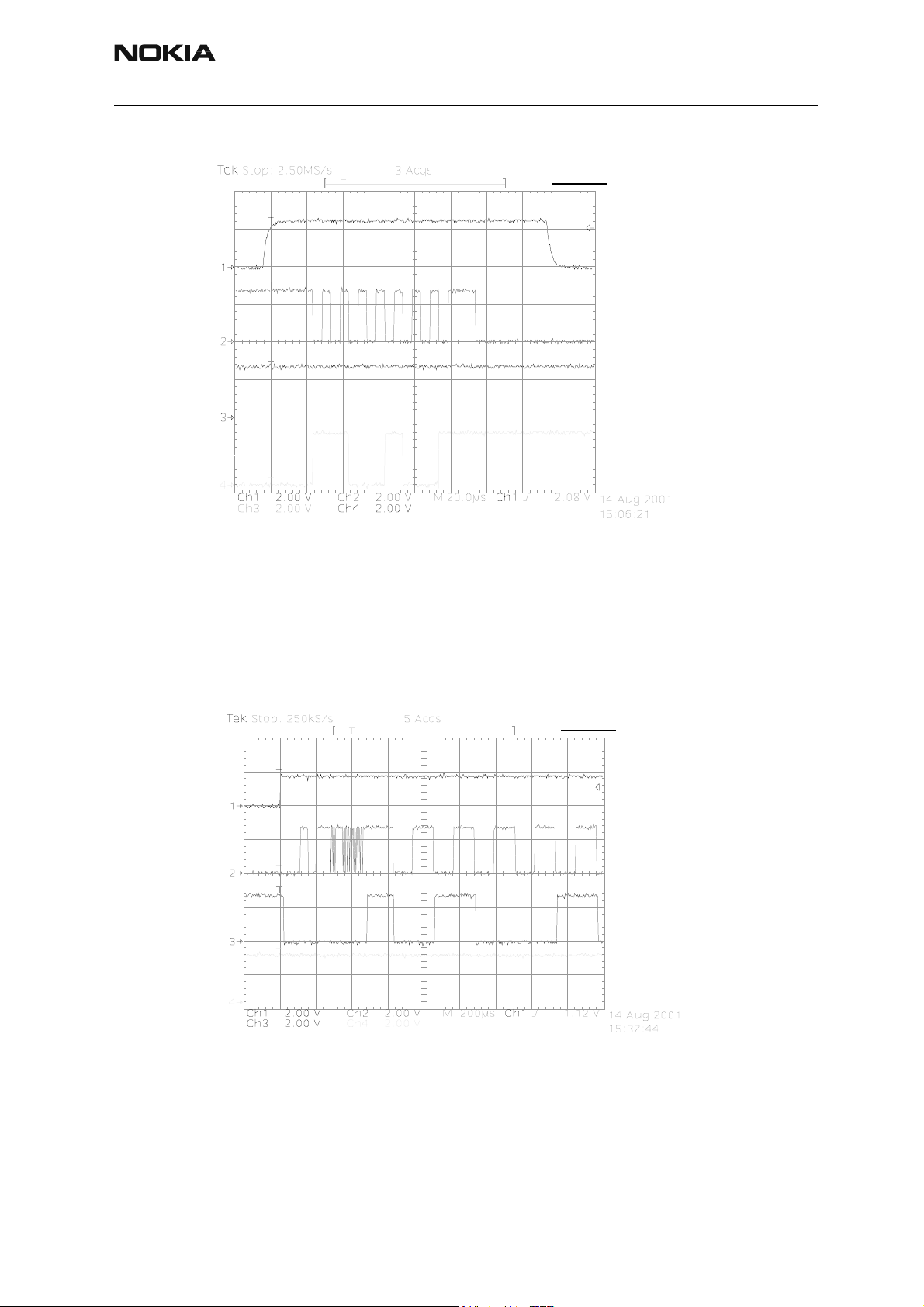
FLASH_1
CH1 = BSI
CH2 = MBUS
CH3 = FBUSTX
CH4 = FBUSR
Measure points
Production test patte
(J396)
Figure 3: Flashing start
• This boot code asks MCU to report prommer phone’s configuration
information, including flash device type. Now, the prommer can select
and send algorithm code to MCU SRAM (and SRAM/Flash self-tests
can be execut ed).
FLASH_2
CH1 = PURX
CH2 = MBUS
CH3 = FBUSTX
CH4 = FBUSRX
Measure points
Production test patter
(J396)
Figure 4: Flashing, continued
Issue 1 05/2002 Nokia Corporation Page 15
Page 16
NHP-2
9. Troubleshooting PAMS Te chnical Documentation
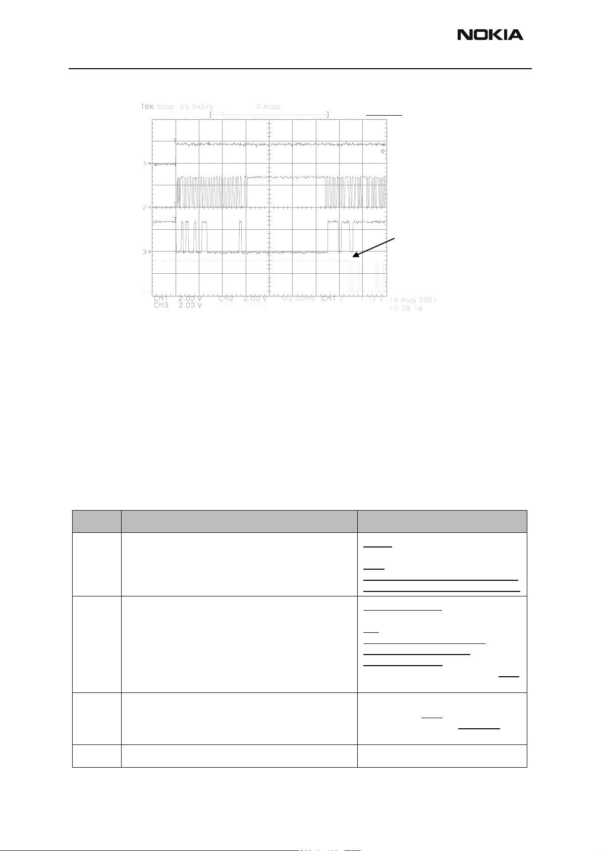
FLASH_3
CH1 = PURX
CH2 = MBUS
CH3 = FBUSTX
CH4 = FBUSRX
Measure points
Produ c tio n te s t pattern
(J396)
Data transfer has
started (Fbus_Rx)
Figure 5: Flashing, continued
Flash programming error codes
• Error codes can be seen from the test results or from Phoenix's flashtool*
• Underlined note means that the connection un der consid eration is being
used for the first time.
• Some error codes may be added later. Here are the most common
ones.
Table 3: Flash programming error codes
Error Description Not working properly
C101
C102
"The Phone does not set FbusTx line high after the startup." Vflash1
VBatt
BSI and FbusRX from prommer to UEM.
FbusTx from UPP->UEM->Prommer(SA0)
"The Phone does not set FbusTx line low after the line has
been high. The Prommer generates this error also when the
Phone is not connected to the Prommer."
PURX(also to Safari)
VR3
Rfclock(VCTCXO->Safari->UPP)
Mbus from Prommer->UEM>UPP(MbusRx)(SA0)
FbusTx from UPP->UEM->P rommer(SA 1)
BSI and FbusRX from prommer to UEM.
C103
C104
" Boot serial line fail." Mbus from Prommer->UEM-
>UPP(MbusRx)(SA1)
FbusRx from Prommer->UEM->UPP
FbusTx from UPP->UEM->Prommer
"MCU ID message sending failed in the Phone." FbusTx from UPP->UEM->Prommer
Page 16 Nokia Corporation Issue 1 05/2002
Page 17
NHP-2
PAMS Technical Documentation 9. Troubleshooting
C105
C106
C107
C586
C686
Cx81
Cx82
A204
Cx83
Cx84
Cx85
"The Phone has not received Secondary boot codes length
bytes correctly."
"The Phone has not received Secondary code bytes correctly." Mbus from Prommer->UEM-
"The Phone MCU can not start Secondary code correctly." UPP
"The erasing status response from the Phone informs about
fail."
"The programming status response from the Phone informs
about fail."
"The Prommer has detected a checksum error in the message,
which it has received from the Phone."
"The Prommer has detected a wrong ID byte in the message,
which it has received from the Phone."
" The flash manufacturer and device Ids in the existing Algorithm files do not match with the Ids received from the target
phone."
"The Prommer has not received Phone acknowledge to the
message."
"The Phone has generated NAK signal during data block transfer."
"Data block handling timeout"
Mbus from Prommer->UEM>UPP(MbusRx)
FbusRx from Prommer->UEM->UPP
FbusTx from UPP->UEM->Prommer
>UPP(MbusRx)
FbusRx from Prommer->UEM->UPP
FbusTx from UPP->UEM->Prommer
Flash
Flash
FbusTx from UPP->UEM->Prommer
FbusTx from UPP->UEM->Prommer
Flash
UPP
VIO/VANA?
Signals between UPP-Flash
Mbus from Prommer->UEM>UPP(MbusRx)
FbusRx from Prommer->UEM->UPP
FbusTx from UPP->UEM->Prommer
Cx87
Startup
for
flashing
"Wrong MCU ID." RFClock
UPP(Vcore)
Required startup for flashing Vflash1
VBatt
Issue 1 05/2002 Nokia Corporation Page 17
Page 18
NHP-2
9. Troubleshooting PAMS Te chnical Documentation
Flash programming
Flash faults
Phone does not set
Flashbus TXD line high
after start up
No
Measure BSI pulse during
Flash programming.
Yes
Measure FBusRx (2.78V)
signal during flash
programming from bottom
connector and test point
J412 (1.8V).
Is it the same?
Measure test point J411
(1.8V) and FBusTx signal
(2.78V) during flash
programming from bottom
connector.
Are they the same?
Is it OK?
Yes
Yes
No
No
No
Check BSI line X101, C230,
R206, C109, R202
Check R102, C103, and
R104.
If OK, then Change UEM.
Change UPP
No
Is there a pulse on J411?
Phone does not set
Flashbus TXD line low after
the line has been high
No
Change UEM
Yes
Measure MBus (2.78V) and
test point J410 (1.8V).
Are they the same?
Yes
Is pulse getting to test point
Yes
J410?
Change UEM
Yes
No
Is there a pulse on
FBusTx?
No
Check R100 and C101.
If OK, then change UEM.
No
Check R101 and C104
No
Is pulse getting to UEM?
Yes
Page 18 Nokia Corporation Issue 1 05/2002
Page 19

NHP-2
PAMS Technical Documentation 9. Troubleshooting
Can you read the
manufacturer ID and the
device ID?
Yes
Is the phone totally dead?
No
Yes
Change Flash
See Phone is dead
flowchart.
Phone doesn't start up or
phone is jammed.
Charging Operation
A Lithium-ion battery with a capacity of 920 mAh is used in NHP-2. Temperature and
capacity information are needed for charge control. These resistors are connected to the
BSI and BTEMP pins of battery connector. The phone has 100 kW pull-up resistors for
these lines so that they can be read by A/D inputs in the phone.
No
No
Retest
Yes
See Phone is jammed
flowchart.
Issue 1 05/2002 Nokia Corporation Page 19
Page 20

NHP-2
4
V100
9. Troubleshooting PAMS Te chnical Documentation
Charging circuitry
The UEM ASIC controls charging, depending on the charger being used and the battery
size. External components are needed for EMC, reverse polarity, and transient protection
of the input to the baseband module. The charger connection is through the system connector interface. NHP-2 baseband is designed to support DCT3 chargers from an electrical point of view. Both two- and three-wire chargers are supported.
(GND)
3(BTEMP)
Figure 6: BLB-3 battery pack pin order
2(BSI)
1 (+)
R200
battery
Figure 7: Charging circuitry
Charger Detection
Connecting a charger creates voltage on VCHAR input of the UEM. When VCHAR input
voltage level is detected to rise above 2 V (VCHdet+threshold) by UEM, charging starts.
VCHARDET signal is generated to indicate the presence of the charger for the SW. The
charger identification/acceptance is controlled by EM SW.
The charger recognition is initiated when the EM SW receives a “charger connected”
interrupt. The algorithm basically consists of the following three steps:
1 Check that the charger output (voltage and current) is within safety limits.
Page 20 Nokia Corporation Issue 1 05/2002
Page 21

NHP-2
)
PAMS Technical Documentation 9. Troubleshooting
2 Identify the charger as a two-wire or three-wire charger.
3 Check that the charger is within the charger window (voltage and current).
If the charger is accepted and identified, the appropriate charging algorithm is initiated.
X100
1, 3
4, 5
F100
1.5A
R107 R108
10K 10K
L100
________
42R/100MHz
D100 C100
C107
10n
Figure 8: Charging circuit
"VCHARIN"
1n0
"PWMO"
0
2
1
CHARGER(4:0
Issue 1 05/2002 Nokia Corporation Page 21
Page 22

NHP-2
9. Troubleshooting PAMS Te chnical Documentation
Charger troubleshooting
Connect charger. Make
sure battery is connected.
Battery bar doesn't work
(scroll)
Yes
Measure voltage over
D100. Is it >3.0 Vdc?
Yes
Read BTEMP value. Is it
- 25C (0319)?
Yes
No
No
No
Retest
Check X100, F100, L100,
D100, C100
Change UEM
Remove (fuse) F100 and
measure current.
Is it -350-390 mA?
No
Change UEM
RetestYes
Page 22 Nokia Corporation Issue 1 05/2002
Page 23

NHP-2
PAMS Technical Documentation 9. Troubleshooting
Display and Keyboard
LEDs are used for LCK and keypad illumination in NHP-2. There are six LEDs for the LCD
and six LEDs for the keypad.
A black/white LCD is used in NHP-2. Interface uses 9-bit data transfer. The interface is
similar to DCT3-type interface, except that Command/Data information is transferred
together with the data. D/C bit set during each transmitted byte.
Issue 1 05/2002 Nokia Corporation Page 23
Page 24

NHP-2
9. Troubleshooting PAMS Te chnical Documentation
Display faults
Are the UI module's LE Ds
turned on after phone is
turned on or when making a
phone call?
No No
Set phone in Local Mode. Use Phoenix "Message
Sender" and navigate as follows: DEV _HOST ->
DEV_PC -> PN_LIGHT -> OBJ_ROUTING_REQ ->
>LIGHT_CONTROL_TARGER_KBD. Select
Measure VBATT voltage at
R302 and R30. Is it OK?
Yes
OBJ_PC -> UTID -
"LIGHT_STATE_BLINK" and cl ick "Send"
Check VBATT line
Measure UEM signal on
V305, V306, V307, V308,
V314, V315.
Is the signal OK?
Yes
No
Change UEM
Change LEDs
Page 24 Nokia Corporation Issue 1 05/2002
Page 25

NHP-2
PAMS Technical Documentation 9. Troubleshooting
Are the display module
LEDs turned on when
phone is turned on or when
making a phone call?
Measure VBATT voltage at
No No
Set phone in Local Mode. Use Phoenix
"Message Sender" and navigate as foll ows:
DEV_HOST -> DEV_PC -> PN_LIGHT ->
OBJ_ROUTING_REQ -> OBJ_PC -> UTID ->
LIGHT_CONTROL_TARGER_DISPLAY.
Select "LIGHT_STATE_BLINK " and click
R302 and R300.
Is it OK?
Yes
LIGHT_CONTROL_REQ ->
"Send"
Measure UEM signal on
V300, V301, V302, V303,
V310, V311.
Is the signal OK?
No
Check VBATT line
Change UEM
Yes
Change LEDs
Issue 1 05/2002 Nokia Corporation Page 25
Page 26

NHP-2
9. Troubleshooting PAMS Te chnical Documentation
Does the display start?
No Yes
Set phone in Local Mode. Use Phoenix
"Message Sender" and navigate as foll ows:
DEV_HOST -> DEV_PC -> PN_TEST ->
OBJ_ROUTING_REQ -> OBJ_PC -> UTID ->
TEST_DISPLAY_SEt -> NUM_SB: ->
TEST_SB_UI_DISPLAY_PATTERN ->
"TEST_PATTERN_ALTPIXELS" and clic k
Try changing display
module.
Does it work?
No
TEST_UI_TEST_REQ ->
SB_LENGTH. Select
"Send"
Check test points J307,
J308, and J309.
Are signals OK?
(Refer to Display Section).
No
Retest
Change UPP
Yes
Change Display
Page 26 Nokia Corporation Issue 1 05/2002
Page 27

NHP-2
PAMS Technical Documentation 9. Troubleshooting
Keypad faults
Is the power key working?
Measure voltage at S300
when power key is pressed.
Is it High?
No No
Measure voltage at S300.
Is it High?
Yes
Yes Yes
No
Check S300. Is it OK?
No
Check S300, C305, and
R304.
If OK, change UEM.
See Phone is
Dead flowchart
Change S300
See Phone is
Jammed
flowchart
Issue 1 05/2002 Nokia Corporation Page 27
Page 28

NHP-2
9. Troubleshooting PAMS Te chnical Documentation
Are the UI module keys
working?
Change keypads module.
Is it working?
No
Measure ROW 0-4 signals
between UPP and Z300.
Are they -1.8V?
Yes
Measure ROW 0-4 signals
between Z300 and
keypads.
Are they -1.8V?
No
No
RetestNo Yes
Make sure there are no
shorts on Z300.
If OK, change UPP.
Change Z300
Yes
Make sure there are no
shorts on Z300.
If OK, change UPP.
Page 28 Nokia Corporation Issue 1 05/2002
Page 29

NHP-2
PAMS Technical Documentation 9. Troubleshooting
Is the volume UP key
working?
Yes
Is the volume DOWN key
working?
No No
Measure S0 (P00) of UPP
Hold down the UP key and
Measure S0 (P15) of UPP
No No
at S301.
Is it 1.8V?
Yes
remeasure.
Is it 1.8V?
Yes
at S301.
Is it 1.8V?
No
Check S301 lines.
If OK, change UPP.
Change UPP
Change S301
Check S301 lines.
If OK, change UPP
Audio
Yes
Hold down the DOWN key
and remeasure.
Is it 1.8V?
Yes
No
Change UPP
Change S301
Audio control and processing in NHP-2 is accomplished by UEM, which contains the
audio codec, and by UPP, which contains the MCU and DSP blocks, handling and processing the audio data signals.
The baseband supports three microphone inputs and two earpiece outputs. Microphone
Issue 1 05/2002 Nokia Corporation Page 29
Page 30

NHP-2
9. Troubleshooting PAMS Te chnical Documentation
inputs are MIC1, MIC2, and MIC3. MIC1 input is used for the phone’s internal microphone; MIC2 input is used for headsets or loopset. MIC3 input is used for third-party
accessories (2.5mm Jack).
Every microphone input can have either a differential or single-ended AC connection to
UEM circuit. In NHP-2, the internal microphone (MIC1) is differential, whereas MIC2 and
MIC3 microphones for accessory detection are single-ended. The microphone signals
from different sources are connected to separate inputs at UEM. Inputs for the microphone signals are differential type. Also, MICBIAS1 is used for MIC1 and MIC3 and
MICBIAS2 is used for MIC2.
Accessories
NHP-2 supports single-ended external audio accessory connection. Headset and data
cables can be connected directly to the system connector or 2.5mm jack supporting TTY/
TDD or third-party accessories. Detection of different accessories is made in analog mode
by reading the DC voltage value of its corresponding AD converter. The following table
indicates accessory detection levels.
Columbia Accessory Detection Table Limits
ADC Upper
Accessory ADC Lower Limit
Type Voltage Hex Voltage Hex HEADINT KEYB1 Detection answer/end call
Value Value Value Value
HEADINT
HDC_9P 0.50V 0x012 400mV 0x094 X N/A
HEADINT N/A
HDE-1 0.50V 0x012 400mV 0x094 X N/A
HEADINT N/A
LPS-1 0.50V 0x012 400mV 0x094
HEADINT N/A
DLR-3P 500mV 0x0B9 850mV 0x13A
JBA-4 900mV 0x14B 1400mV 0x202 X N/A
Third Party
Acc. 0.50V 0x012 1.0V 0x170 N/A X
GenIO21 N/A
TTY/TDD 2.40V 0x374 2.78V 0x3FF N/A X
Limit ADC used Interrupt Interrupt to
HOOKIN
T
X
X
N/A
N/A
HEADINT N/A
GenIO21 N/A
Page 30 Nokia Corporation Issue 1 05/2002
Page 31

NHP-2
PAMS Technical Documentation 9. Troubleshooting
Audio Troubleshooting
Earpiece failure
Is the earpiece working?
No Yes
Change earpiece.
Is it working now?
No
Set phone in LOCAL mode. Use
Phoenix "Baseband Audio
Control" and set the following:
Enable Tx, Enable Rx, Select
MIC2 (0dB), Enable earpiece
only. Inject 1KHz sine signal
200mVpp on XEAR.
Is the signal coming out of
the UEM on EARP and
EARN?
No
Retest
Check R161, R159, C156,
R173, C154, C155, R152,
R154, C150, C152.
If OK, change UEM.
Yes
Check R150, C180, and
If OK, change earpiece.
C161.
Issue 1 05/2002 Nokia Corporation Page 31
Page 32

NHP-2
9. Troubleshooting PAMS Te chnical Documentation
Microphone failure
Is the microphone working?
No Yes
Change the microphone. Is
it working now?
No
Set phone in Local Mode.
Use Phoenix "Baseband
Audio Control" and set the
following: Enable Tx,
Enable Rx, Select MIC1,
Enable HF only (single-
ended). Talk through the
microphone.
Measure MICB1 voltage
from MICP pads on bott o m
connector. Is it -2.1V?
Yes
No
Retest
Check C195, R176, C176,
R167, C174, C175, R172,
R164, C170, C172. If OK,
change UEM.
Is the signal going to the
UEM at MICP and MICN at
C170 and C172?
Yes
Is the signal going out of
the UEM at XEAR, pin 10
on the bottom connector
(X100)?
Yes
No
No
If connection is OK at C170
and C172, then change
microphone.
Check R160 and C164. If
OK, change UEM.
Retest
Page 32 Nokia Corporation Issue 1 05/2002
Page 33

NHP-2
PAMS Technical Documentation 9. Troubleshooting
Vibra failure
Is vibra working?
Measure VBATT voltage
pin 1 of M300. Is it OK?
Yes
Set phone in Local Mode. Use Phoenix "Message
Sender" and navigate as follows: DEV_HOST ->
Dev_PC -> PN_ACCESSORY ->
PN_OBJ_ROUTING_REQ -> PN_OBJ_PC ->
UTID_100 -> ACC_VIBRA_CTRL_REQ. Select
"ACC_ON" and click "Send".
Measure UEM signal on
pin 2 of M300.
Is the signal OK?
NoNo
No
Check VBATT line
Change UEM
Change vibraYes
Issue 1 05/2002 Nokia Corporation Page 33
Page 34

NHP-2
9. Troubleshooting PAMS Te chnical Documentation
Buzzer failure
Is buzzer working?
Measure VBATT voltage
from B302. Is it OK ?
Yes
Set phone in Local Mode.
Use Phoenix "Baseband
Audio Control". Under
Buzzer on Frequency and
Duty cycle input 20.
Check signal on pin 2 of
B302. Is the signal OK?
NoNo
No
Check VBATT line
Change UEM
Change buzzerYes
Page 34 Nokia Corporation Issue 1 05/2002
Page 35

NHP-2
PAMS Technical Documentation 9. Troubleshooting
Receiver fault finding
PCS
RFA
LOA
Cell
RFA
UHF
VCO
PCS
LNA
Cell
LNA
ALFRED
Figure 9: Receiver block diagram
General instructions for RX troubleshooting
Start Phoenix software and use it to start the wanted RX-mode of the mobile phone.
Troubleshooting flowchart is divided into three steps: general checking, local checking,
and RX-chain checking. Notice that before changing ASICs or filter, all solderings and
missing components must be checked visually. After any possible component changes,
the phone must be retuned.
Path of the received signal
AMPS
CDMA
IF
128.1MHz
AMPS
IF XTL
CDMA
IF SAW
VGA
IQ
DEMOD
ADC
I
BBFIL/BBAMP
Q
BATMAN D
Block level description of the receiver:
(Antenna/ext RF) Antenna Switch – Diplexer – Duplexer – Low Noise Amplifier (LNA) –
RX band filter – First mixer – 128.1 MHz RX IF filter – IF-amplifier – second mixer – 614
kHz low-pass filter – adjustable IQ amplifier – Baseband.
Issue 1 05/2002 Nokia Corporation Page 35
Page 36

NHP-2
9. Troubleshooting PAMS Te chnical Documentation
Fault finding charts for receiver chain
AMPS
Using Phoenix,
configure phone AGC
& audio routing to
make SINAD
measurement
Apply 881.49 MHz =
ch 383 -116dBm,
8kHz dev, 1kHz sine
signal to external
RF-connector X800.
YES
Connect HS to cellular
tester; open audio
AF: 1kHz sine signal,
meas SINAD
AF:>12 dB
NO
AMPS RX-chain OK
YES
Check UHF Vc (from
C509) V: 1.8...2.1V
YES
Check RXVHF Vc
(from C715),
V:0.7...1.3
Using Phoenix,
readjust AGC to
obtain proper Rx I/Q
level
NO
NO
Start synthesizer
troubleshooting
Start synthesizer
troubleshooting
Apply 881.49 MHz
-30dBm, sine signal to
external RF-connector
X900.
Page 36 Nokia Corporation Issue 1 05/2002
Page 37

NHP-2
d
of
ou
t
PAMS Technical Documentation 9. Troubleshooting
Note!
Check input level at
diplexer (Z805) input
YES
NO
Change EXT RF
connector
Check all soldering
and components in
antenna circuit before
changing.
Check input level at
duplex filter. You also
can check level at
diplexer output.
YES
Check input level at
LNA input (L750)
YES
Check RF level at cell
band filter input.
NO
NO
NO
Change diplexer
(Z805)
Change duplex filter
(Z804)
Change Alfred N750
Note!
Check all soldering an
discrete components
front end.
Note!
Check all
solderings and
discrete
components
around Alfred
before changing.
YES
Check RF level at
C_Mix_IN
YES
NO
Change Alfred N750
Note!
From beginning to
C_Mix_IN input, y
should see strong
RF signal level at
881.49 MHz. Exac
level is difficult to
define due to
variable
impedances in RX
path. Also, the
probe type used
affects results.
Issue 1 05/2002 Nokia Corporation Page 37
Page 38

NHP-2
r
9. Troubleshooting PAMS Te chnical Documentation
Check RF level at RX
IF filter input
at 128.1 MHz
YES
Check RF level at RX
IF filter output
at 128.1 MHz
Check RF level at
NO NO
NO
PCS_Cell_LO
at 1009.59 MHz
YES
Change UHF PLL
(N501)
Change RX IF filter
(Z752)
Note!
Check all discrete
components and
voltages around
Alfred.
Start UHF synthesize
troubleshoot
YES
Check RX I and Q
signals at I:
R707,R708,R709,
R710
YES
Check UEM and start
baseband
troubleshoot
Check RF level by
NO NO
L701 without having
electrical contact at
256.2 MHz
YES
Change Batman
(N701)
Start synthesizer
troubleshoot
Page 38 Nokia Corporation Issue 1 05/2002
Page 39

NHP-2
PAMS Technical Documentation 9. Troubleshooting
Cell CDMA
Troubleshooting 128.1 MHz IF Saw Filter
Since the same physical signal path is used for both analog and digital modes at the
lower band, there is no need for additional troubleshooting in the digital mode. So if the
digital mode at the lower band is not working properly, start the analog mode troubleshooting.
PCS
st
Only EXT RF connector –> 1
IF needs separate troubleshoot at upper band. After down
conversion (RF –> 128.1 MHz) both lower and upper band use same signal path.
Issue 1 05/2002 Nokia Corporation Page 39
Page 40

NHP-2
9. Troubleshooting PAMS Te chnical Documentation
.
Using Phoenix,
configure RX to
ch 600 and set
appropriate gain.
Apply 1960.0 MHz =
ch 600 -50dBm signal
to external
RF-connector X800.
YES
Check RX I and Q
signals at I:
R707 - R710
NO
Check UHF Vc (from
C509) V: 2.2 ...2.6V
YES
Check RXVHF Vc
(from C715)
V: 0.7 ...1.3
YES
NO
NO
PCS RX-chain is OK
Start synthesizer
troubleshooting
Start synthesizer
troubleshooting
YES
Page 40 Nokia Corporation Issue 1 05/2002
Page 41

NHP-2
PAMS Technical Documentation 9. Troubleshooting
Check input level of
diplexer (Z805)
YES
Check input level of
duplex filter (Z803)
YES
Check RF level at
LNA input (at duplex
filter RX output port)
NO
NO
NO
Change EXT RF
connector
Change diplexer
(Z805)
Change duplex filter
(Z803)
Note!
Check all soldering and
components in antenna
circuit before changing.
Note!
Check all soldering and
discrete components of
front end.
Note!
Before replacing Alfred,
check all the solderings
and components around
N750.
YES
Check RF level at
PCS band filter (Z750)
input
YES
Change Alfred (N750)???NO
Issue 1 05/2002 Nokia Corporation Page 41
Page 42

NHP-2
9. Troubleshooting PAMS Te chnical Documentation
Check RF level at
P_MIX_IN
YES
Check RF level at RX
IF filter input
at 128.1 MHz
YES
Continue
troubleshooting Cell
Band
NO
NO
Change PCS band
filter Z750
Check RF level at
PCS_Cell_LO at
2088.1 MHz
YES
Change UHF PLL
(N501)
NO
Start UHF synthesizer
troubleshooting
Note!
Check all discrete
components and
voltages around
Alfred.
Page 42 Nokia Corporation Issue 1 05/2002
Page 43

NHP-2
PAMS Technical Documentation 9. Troubleshooting
Transmitter fault finding
RX
SPLIT BAND
SAW FILTER
Hi BAND
Lo BAND
CELL
SAW
Filter
Detector
HORNET
TX_RF_AGC
( UPP )
TOMCAT
P_DET
P_REF
WHIP
ANT.
Internal
ANT.
Ant.
Switch
RF
Conn.
RX
PCS DUPLEXERCELL DUPLEXER
Isolator
Diplexer
Isolator
SNAPPER
PA
SHARK
PA
Figure 10: Transmitter block diagram
General instructions for TX troubleshooting
PCS
DVR
CELL
DVR
UHF LO
ROBIN
UP CONV
Current Mirror
PA_AGC
( UPP )
IF AGC
PWROUT
(UEM)
19.2
MHz
CLK
VHF PLL
TX_ IF_AGC
( UPP )
DATA
SIO
Enable
Filter &
Resonator
CLK
Div By 2
I/Q
MODBBFilter
VHF SYNTH
2
I
inputs
Q
2
Always use RF-cable connected from external RF-connector to analyzer via (rf-power)
attenuator. This is important to protect analyzer against excessive rf-power and to prevent unwanted rf-power from leaking to the cellular frequencies.
Start Phoenix software and select TX mode. It is recommended that you select mid channel (383 for AMPS/CDMA or 600 for PCS) and appropriate power level.
Note: Tune the phone after any component change.
Path of the transmitted signal
AMPS/Cell CDMA
UEM TX I/Q DA-converters -> I/Q modulator and VGA (Robin) -> IF ->
Upconverter + driver - EXT Driver amp > BPF -> PA -> (Power detector) -> Duplex-filter
-> Diplexer -> EXT RF-connector -> Cyclops -> Antenna
PCS (ONLY DUALBANDER)
UEM TX I/Q DA-converters -> I/Q modulator and VGA (Robin) -> IF-> Upconverter +
driver ->Balun -> BPF -> PA-> (Power detector) -> Duplex-filter -> Diplexer ->
EXT RF-connector -> Cyclops -> Antenna
l
Power detection and power control circuit belongs under power control part of this
guide.
Issue 1 05/2002 Nokia Corporation Page 43
Page 44

NHP-2
9. Troubleshooting PAMS Te chnical Documentation
Fault finding charts for transmitter
AMPS
Start Phoenix software and set phone to the Analog mode. Set channel 383 and Powerlevel 2. Connect RF-cable to Ext RF connector and connect cable to Spectrum analyzer
input and measure RF level. Please notice insertion loss of the cable and attenuations.
Page 44 Nokia Corporation Issue 1 05/2002
Page 45

NHP-2
PAMS Technical Documentation 9. Troubleshooting
AMPS, PL2, CH383
Visual check of TX
block
-PA and up converter
-TX SAW
-Duplex filter
-Passive components
OK
Check LO-signal
(1009.59 MHz) @ up
converter and TX VHF
(346.2 MHz) @ N601
NO
Start synthesizer
troubleshooting
OK
Check supply voltage
-VR2
-VR3
-VR6
-VR1B
OK
Check TXi/q signals
Test points
R626 - R629
OK
NO
NO
Check UEM and UPP
(baseband)
Check UEM
(baseband)
Check TX RF (836.49
MHz) output power
and @ up converter
RF: 0 dBm +/- 6 dB
OK
NO
Change Robin
Issue 1 05/2002 Nokia Corporation Page 45
Page 46

NHP-2
r
9. Troubleshooting PAMS Te chnical Documentation
Check TX SAW input
and output power
IL: -3dB
OK
Is Itot 700...800 mA?
Check PA output
power and gain.
Output power: -28
dBm
Gain: -30 dB
OK
Check Isolator Z802
insertion loss
IL< 0.3 dB
NO
NO
NO
Change TX SAW filte
Z604
Change PA
N801
Change Isolator
Z802
OK
Check duplexer Z803, diplexer
Z805, and RF connector X800
insertion loss
Dupl IL -2.2 dB
Dipl -0.35 dB
RF conn -0.1 dB
OK
Start Power control
troubleshooting
Cell CDMA
The transmitter chain is exactly same as AMPS mode, except control current. Thus, it is
important that AMPS has no faults.
NO
Change Z803 or Z805
or RF connector
Page 46 Nokia Corporation Issue 1 05/2002
Page 47

NHP-2
PAMS Technical Documentation 9. Troubleshooting
PCS (only dualbander)
PCS mode and Cell CDMA mode have a common RF modulator, making it important that
Cell CDMA mode has no faults.
PCS Cell CDMA,
+24 dBm, CH600
Is Cell CDMA mode
OK?
OK
Check LO-signal
2088.1 MHz @ T775
and TX VHF
116.2 MHz @ N750
OK
Check supply voltage
_VR2
-VBATTRF
-VR3
-VR6
-VR1B
OK
NO
NO
NO
Start AMPS
troubleshooting
Start synthesizer
troubleshooting
Check UEM and UPP
(baseband)
Check TX RF (1880
MHz) output power
@T603 output
RF: 0 dBm +/- 6 dB
OK
Check Z601 input and
output power IL: -3 dB
OK
NO
NO
Change Robin
Change Z601
Issue 1 05/2002 Nokia Corporation Page 47
Page 48

NHP-2
9. Troubleshooting PAMS Te chnical Documentation
Is Itot 350...450 mA?
Check PA output
power and gain.
Output power: -27
dBm
Gain: -30 dB
OK
NO
Change PA
N960
Check Isolator Z801
insertion loss
IL< 0.3 dB
OK
Check duplexer Z804
diplexer Z805 and RF
connector X800 insertion
loss
Dupl IL -2.2 dB
Dipl -0.35 dB
RF conn -0.1 dB
OK
Start Power control
troubleshooting
NO
NO
Change Isolator
Z801
Change Z804 or Z805
or RF connector
Power control loop
Basically power detection is done with circuitry and power control is done inside Robin
and PA. Power detection is basically similar for both bands, except both bands have individual couplers.
Page 48 Nokia Corporation Issue 1 05/2002
Page 49

NHP-2
Detected voltages are described in the next table and diagram.
T
N
PAMS Technical Documentation 9. Troubleshooting
Note!
Is PWRDET vs.
output power OK?
See chart below.
YES
NO
Check VR2.
Check PWRDET
circuitry.
See
PWRDET
vs. Output
power curve
Is DAC value vs.
PWRDET (mV) OK?
NO
Check UEM
(baseband)
YPICAL DETECTED VOLTAGES AT POWER LEVELS PL2…PL10 FOR DUALBANDER
800A 800D 1900D
Pout TXPWRDET Pout TXPWRDET Pout TXPWRDET
PL dBm dac mV dBm dac mV dBm dac mV
2 26.5 633 1671 27.3 696 1839 27.3 662 1746
3 22.5 393 1038 23.3 433 1142 23.3 405 1069
4 18.5 237 625 19.3 261 688 19.3 245 648
5 14.5 141 372 15.3 155 410 15.3 147 387
6 10.5 82 215 11.3 90 237 11.3 84 222
7 6.5 46 120 7.3 50 132 7.3 46 122
8 - - - 3.3 27 70 3.3 24 64
9 - - - -0.7 13 33 -0.7 11 30
10 - - - -4.7 5 12 -4.7 5 12
OTE: DAC VALUES MAY VARY ABOUT +/- 20%
Issue 1 05/2002 Nokia Corporation Page 49
Page 50

NHP-2
9. Troubleshooting PAMS Te chnical Documentation
2000
1800
1600
1400
Detected voltage [mV]
1200
1000
800
600
400
200
0
246810
Power level
800A
800D
1900D
Page 50 Nokia Corporation Issue 1 05/2002
Page 51

NHP-2
PAMS Technical Documentation 9. Troubleshooting
Synthesizer fault finding
There are four oscillators generating the needed frequencies for RF-section. 19.2 MHz
reference oscillator, 1 GHz and 2GHz UHF VCO, TX VHF VCO, and RX VHF VCO. RX VHF
frequency is fixed 256.2 MHz and TX VHF has two fixed frequencies: 246.2 MHz for lowband and 416.2 MHz for upper band. UHF VCO's operating frequencíes are controlled by
PLL-circuit of LMX2370I. All locals are locked to stable 19.2 MHz reference oscillator.
The frequency range for UHF VCO is two separate bands. The output frequency range for
the lower band is from 997.11 MHz to 1022.07 MHz. In upper band, the output frequency
range from the UHF VCO is from 2058.1 MHz to 2118.05 MHz.
It is practical to check out the synthesizer status by measuring control voltage of the
VCO from the Integrator capacitor. If the voltage is stable and reasonable, local oscillators are running correctly.
19.2 MHz reference oscillator
The 19.2 MHz oscillator frequency (G790) is controlled by UEM. This 19.2 MHz signal is
connected to Batman/Robin and there in PLL-circuits and to UPP.
All synthesizers use divided VCTCXO signal as a reference signal for Phase locked loop to
provide correct LO-frequency.
Baseband needs a reference signal where it can generate the necessary clock signals and
VCTCXO output signal is also buffered and connected to UPP.
Issue 1 05/2002 Nokia Corporation Page 51
Page 52

NHP-2
9. Troubleshooting PAMS Te chnical Documentation
Fault finding chart for 19.2 MHz oscillator
Start Here!
2 Change VCTCXO
OK
2.No
Is VCTCXO
oscillating?
19.2 MHz
1.No
OK
1 Check voltage
C505
2.78 V
OK
RX VHF VCO
The RX VHF VCO signal is used to generate receiver Intermediate frequency. RX VHF VCO
has one fixed frequency 256.2 MHz. Operating frequency is locked in Phase-locked Loop.
RX VHF VCO output signal is fed to Batman. Inside, the Batman signal is divided for
Phase detector and RX parts. Before I/Q-modulator frequency is divided by 2.
No
OK
Check resistor
Page 52 Nokia Corporation Issue 1 05/2002
Page 53

NHP-2
PAMS Technical Documentation 9. Troubleshooting
Fault finding chart for RX VHF VCO
Measure oscillator frequency over L701 coil. Don´t connect probe to pads!
AMPS, CH383
4
Change Batman
NO
NO
OK
TX VHF Synth
The TX VHF VCO signal is used to generate transmitter Intermediate frequency. TX VHF
VCO has two fixed frequencies: 346.2 MHz for lower band and 416.2 MHz for upper
band. Operating frequency is locked in Phase-locked Loop and frequency is divided by
two before modulator.
3
Check loop filter
components:
C701,R714,C715,
R703,R702,C704
1
3.No YES
3.No
OK
Start Here.
Is oscillator locked to
256.2 MHz?
OK
OK 2.No
2
Check resonator
components:
V701,C716,L701, and
DC block C702
OK
Issue 1 05/2002 Nokia Corporation Page 53
Page 54

NHP-2
9. Troubleshooting PAMS Te chnical Documentation
Fault finding chart for TX VHF VCO
AMPS, CH383 -> TX VHF frequency 346.2 MHz
PCS, CH600 -> TX VHF frequency 416.2 MHz
4
Check components:
C612,C613,C632
R607,R605,R606
O
K
4
.
N
o
5
Change
Robin
OK
3
Check resonator
components:
V601,C631,L611,
C630,C629,V602,
C637,C638
OK
5.No
1
Start Here
Is oscillator locked to
346.2 MHz or 416.2
MHz?
o
N
.
3
2.No OK
K
O
s
e
Y
UHF Synthesizer
The UHF synthesizer consists of an external UHF VCO, loop filter and integrated PLL in
LMX2370 N501. IC contains stages like counters, prescaler, divider by two, phase and frequency comparator, and a charge pump circuit.
The output frequency of the VCO depends on the DC-control voltage, which is controlled
by PLL-circuit inside N501.
2
Check operating
voltage:
2.78 V at R609
No
OK
Check:
R609
Page 54 Nokia Corporation Issue 1 05/2002
Page 55

NHP-2
PAMS Technical Documentation 9. Troubleshooting
Fault finding chart for UHF Synthesizer
Change VCO
OK
Change N501
3.No
4.No
Is frequency locked?
2.No
OK
Check loopfilter
components and
balun
START HERE
1.No
OK
Check VCO operating
voltage: 2.78V
No
OK
Is EVM OK?
No OK
1
Check loopfilter
components
Check r esistor R515
Yes
NoYes
OK
Issue 1 05/2002 Nokia Corporation Page 55
Page 56

NHP-2
9. Troubleshooting PAMS Te chnical Documentation
Test Point Diagrams
Test points (TPD) are illustrated in the following diagrams.
Figure 11: Test points — top view A
Page 56 Nokia Corporation Issue 1 05/2002
Page 57

NHP-2
PAMS Technical Documentation 9. Troubleshooting
Figure 12: Test points — top view B
Issue 1 05/2002 Nokia Corporation Page 57
Page 58

NHP-2
9. Troubleshooting PAMS Te chnical Documentation
Figure 13: Test points — bottom view A
Page 58 Nokia Corporation Issue 1 05/2002
Page 59

NHP-2
PAMS Technical Documentation 9. Troubleshooting
Figure 14: Test points — bottom view B
Issue 1 05/2002 Nokia Corporation Page 59
Page 60

NHP-2
9. Troubleshooting PAMS Te chnical Documentation
Page 60 Nokia Corporation Issue 1 05/2002
 Loading...