

Page 1

After Sales Technical Documentation
TROUBLESHOOTING
INSTRUCTIONS
FOR NHA–2 & NHA–4
Original, 43/96 NMP Part No. 0275035
Page 2
Troubleshooting Instructions
AMENDMENT RECORD SHEET
After Sales
Technical Documentation
Amendment
Number
Date Inserted By Comments
Page 2
Original, 45/95
Page 3

After Sales
Technical Documentation
TROUBLESHOOTING INSTRUCTIONS
Contents
Introduction Page 4
General Page 4
General Chart Page 5
Logic Fault Page 6
Receiver Fault 1 Page 7
Receiver Fault 2 Page 8
Transmitter Fault 1 Page 9
Transmitter Fault 2 Page 10
Earphone Level/Modulation Level Fault Page 11
Display or Keypad Fault Page 12
Call Set–up Fault Page 13
Troubleshooting Instructions
Original, 45/95
Page 3
Page 4

Troubleshooting Instructions
Introduction
General
The purpose is to define fault block of the module and then find out the broken
component. The trouble shooting diagram has been planned so that the fault,
whatever it is, can be found by as simple measurements as possible.
The flow diagrams give you the overview of the blocks. The purpose is that you
proceed through the flow diagram so that, if your answer is YES for the asked
question, go straight to the next level, but if your answer is NO, you have to go
the subbranch.
Required servicing equipment:
– PC for PC locals
– Power supply (2.0 A)
– Digital multimeter
After Sales
Technical Documentation
– Oscilloscope
– RF cables
– Modular cable
– RS232/MBUS adapter
– CMT/Marconi
– RF measuring chassis
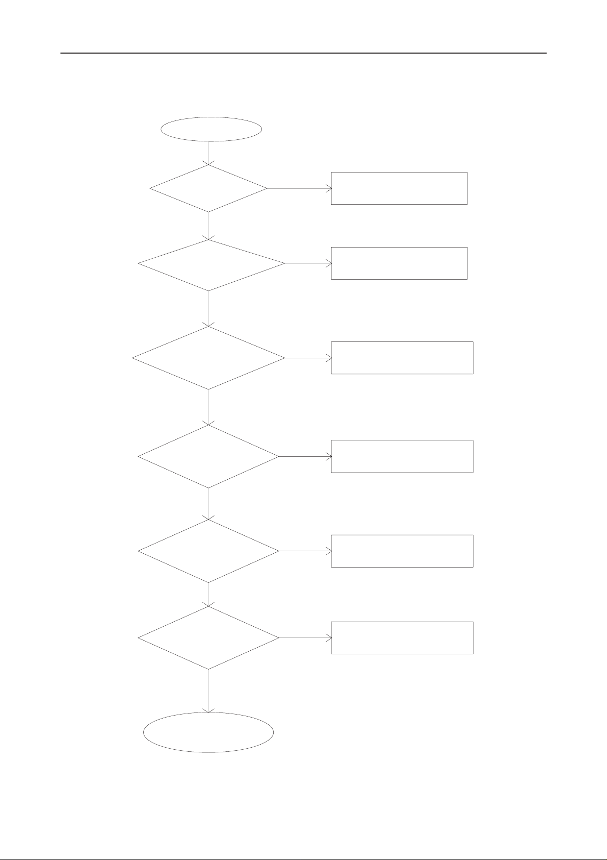
The Troubleshooting for NHA–2 consist of 8 consequent checks according to
the following flow diagram.
Page 4
Original, 45/95
Page 5
After Sales
Technical Documentation
General Chart
Troubleshooting Instructions
START
Will turn into
local mode ?
Receiver OK ?
( SINAD OK )
Transmitter operating
( RF power OK ) ?
Earphone level /
modulation
Yes
Yes
Yes
No
No
No
No
Logic fault
Receiver fault
Transmitter fault
Earphone level or
modulation fault
Is display / keypad
working ?
Call set–up ?
END
Yes
Yes
Yes
No
No
Display or keypad fault
Call set–up fault
Original, 45/95
Page 5
Page 6

Page 6
Logic Fault
Troubleshooting Instructions
Original, 45/95
Logic fault
Power drops off or
does not assume
local mode.
Check clock
signal of N2/pin 61
0.8 Vpp/14.85 MHz
OK ?
YES
Is RESET 0V
in N1/pin 10 ?
YES
Check :
– loading of N1/pin 10
– CRESET N1/pin 20 2.4V
– VCHAR N1/pin 21 0.7 V
NO
NO
Are VL (N1/pin 23)
and VA (N1/pin 2)
3.3 V ?
Check:
– solderings of G600
– loading of CLKIN–line
– C77
– if OK, change G600
Check CLKMCU
of N2/pin 63
3.5 Vpp/2.4 MHz .
OK ?
Check :
– D1/ VA, VL, GND, data and adress lines
– N1/pin 11 TXD 3.3 V
– N1/pin 12 3.3 V
– loading of RXD line
– loading of MBUS line
– if OK, change D1
YES
YES
NO
Is
G600 / VCC
3.6 V ?
NO
Check :
– COFF N1/pin 16 2 Vpp
– VBAT N1/pins 1, 5 and 22 4.8 V
– GND N1/pins 7, 19 and 24
– CREF N1/pin 6 3.3 V
– if OK, change N1
Check :
– loading of VRXI–line
NOYES
Check :
– loading of CLKMCU line
– solderings of N2
– if OK, change N2
– R717 and R718
– VREF–line
– the components
affecting V901 and
V902 d.c. operating
points
Technical Documentation
After Sales
Page 7

After Sales
Technical Documentation
Receiver Fault 1
Check :
– loading of VREF line
– if OK, change N1
Check the components
affecting V901 and
V902 d.c. operating
points
No
Troubleshooting Instructions
Is VREF
( R906 ) 3.3V ?
Are VRXI
and RXBIAS
( V700/c ) 3.65 V
AF signal at
R716 DAF line
Yes
Is VRX
Yes
( V700/b ) 2.6 V ?
( C901 ) 3.7 V ?
Is ( VCC )
1.85 V
N700/pin 4
Yes
Yes
Check :
– R717
– loading of RXI line
– RXBIAS line
Check IF demodulator circuit
C727, solderings of N700,
N700/pin 9 and R716
L704, C723, R712, R715, C722,
C706 and C705
Check :
– the operation between
– V703 d.c. voltages
3–5–10–11
at different pins
Check :
– solderings of N700
– 2nd IF line N700/
– N700 d.c. voltages
45 MHz ?
Is there at
C705 – 34dBm*/
No
Yes Yes
Yes
Earphone
level fault
Check R702,
V700 d.c. operation
point
No No
Check solderings of Z703,
L706, C706, Z702, V701
and C716
Check level at
45 MHz. OK ?
C706 – 51dBm*/
*measured with 10:1 divider
Original, 45/95
Receiver fault
Noise or AF signal
at X1/pin 9 XEAR
No No No No No
Simplex sens.
( TX off ) OK?
Yes
Yes
Transmitter
No
TX spectrum
fault
OK ?
Test point
2.5 – 4.0 V
RXVCO, middle channel
No
fault 2
Receiver
Yes
filter Z700
Replace duplex
Yes
Injektion level
at C709 – 16dBm*
No
Check solderings of
Yes
V601, C600, C602
and C709
?
Is there at
44.55 MHz
N700/pin 2 – 28dBm*/
No
Check solderings
of R636, C749, C718,
C719 and L710.
Check also N700/
pins 1 and 2.
Yes
Yes
Is there level
at Z703 – 63dBm* ?
No
Check the operation
between the aerial
and Z703
Page 7
Page 8

Troubleshooting Instructions
Receiver Fault 2
Receiver fault 1
After Sales
Technical Documentation
*measured with 10:1 divider
Check L603
– 1.9 V. OK ?
Yes
Are N650/
pins 4 and 14
2.8 V ?
Yes
Control signals
of N650/pins 8, 11, 12,
13, 19 ( pin 8 –17dBm*/
14.85 MHz )
OK ?
Yes
Check d.c voltages :
V601/c (3.7V) b (2.0V) e (1.3V)
V602/c (3.2V) b (1.6V) e (0.9V)
OK ?
No
No
No
No
Check –VMOD line
between display module
( or –VOUT pad ) and
V603 anode
Check :
– L605, V605, R646, R647
– loading of N650/pins 4 and 14
Check following lines :
– D1/pin 13 ( SDATA )
– D1/pin 17 ( SCLK )
– D1/pin 18 ( SLE )
– D1/pin 26 ( SLD )
Check G600 and C669
Check :
– V700/b ( RXBIAS ) 2.6 V
– V604 d.c voltages
– the components affecting
V601 and V602 d.c.
operating points
Yes
Resistance
between N650/pin 3
and V603 8.2 Kohm
Yes
Is RXVCO
oscillating at
V602 collector ?
( – 28 dBm* )
Yes
Is level to
prescaler N650/
pin 6 – 30dBm* ?
Yes
Check the critical components
of VCO : C604, V603, C614,
C613, C612, C601
No
No
No
Fault in loop filter
Check the critical components
of VCO : C604, V603, C614,
C613, C612, C601
C600, R600, R614 or
the freguency of VCO
is substantially off
the mark ( C604, V603,
C614, C613, C612, C601 )
Page 8
Original, 45/95
Page 9

After Sales
Technical Documentation
Transmitter Fault 1
Check loading
of TXS line.
If OK, change D1.
Check
3.3V
TXS D1/pin 21
Check :
– V654 and V651
– the components affecting
operating points
V654 and V651 d.c.
Troubleshooting Instructions
Check the operation
between the components
R625 and C662.
Measure level at L653
–17dBm*/90 MHz
Check the operation
between the components
C662 and C804.
Yes Yes
3.5 V
Check V662
collector ( TSYN )
Yes
Current
consumption
level >= 450mA
of biggest power
No No No No
Yes
error
frequency
Power OK,
Transmitter fault
but transmitter
*measured with 10:1 divider
Is there
Check duplex filter
Z700 TX port solder
joint, path from
V805 collector
Check the operation
of G600 and its
eeprom values
Yes
90 MHz ?
about 3 V at
testpoint TXVCO
and at L653 –17dBm*/
No
Check the operation of
the differential amplifier
Transmitter fault 2
( V807, V809, V808 )
No
–19dBm* ?
Is there at
V662 collector
No
Check the critical
Yes
4 V.
Check that
collector is
VCONT at V803
Yes
components of
the amplifier V803
No
Yes
Is there at
–14dBm* ?
V660 collector
No
Is there at
No
Check the components
affecting V804 d.c.
operating point
–4dBm*
V803 collector
( biggest power ) ?
YesYes
Is there
+2dBm* ?
at V804 collector
Original, 45/95
Check the
components
affecting V805
d.c. operating
point
Page 9
Page 10

Page 10
Transmitter fault 1
Transmitter Fault 2
Troubleshooting Instructions
Original, 45/95
Resistance between
N650/pin 17 and V659
cathode is about 5 Kohm
Fault in loop filter
Check d.c.voltages
Yes Yes
V657/c (2.7V) b (2.7V) e (2.0V)
V658/c (1.8V) b (1.1V) e (0.5V)
OK ?
NoNo
Check the components
affecting V657 and V658
d.c. operating points
Check the critical
components of VCO :
V659, C663, C659, L651,
C675. Check also C686,
C637 and N650/pin 15.
Technical Documentation
After Sales
Page 11

After Sales
Technical Documentation
Earphone Level/Modulation Level Fault
ST 1.7 Vpp
SAT 420mVpp
MOD
LPIN
Troubleshooting Instructions
X1/pin 9
XEAR
330 mVpp
pin 52 pin 53 pin 55
pin 51
EMPI EMPO
pin 50
COMO
pin 49
COMI
pin 47
ATTO
120 mVpp 120 mVpp 190 mVpp 190mVpp 270 mVpp 270 mVpp 540 mVpp
pin 35
XEAR
pin 34
VOLI
pin 32
EXPO
pin 29
EXPI
pin 28
FILO
Original, 45/95
– voice modulation 2.9 kHz
– volume 3
– comp. on
– XMIC line 60 mV / 1 kHz
Signals levels of N2
pin 46
XMIC
140 mVpp
pin 27
DAF
140 mVpp 200 mVpp 200 mVpp 140 mVpp 140 mVpp 330 mVpp
Page 11
Page 12

Troubleshooting Instructions
Display or Keypad Fault
Display or keypad fault
After Sales
Technical Documentation
Display OK ?
Yes
Check :
– loading of –VOUT
– soldering of X2/pin 5
No
No
Change the
display module
Display OK ?
Lights OK ?
–VOUT OK ?
Pulses to
0V on COL 0–3
lines
Yes
Yes
Yes
Check:
– X2/pins 1 and 15 ( VBAT )
– X2/pins 4 and 16 ( GND )
– X2/pin 3 ( LCDCLK ) 2Vpp / 80 kHz
– X2/pin 7 ( RESET ) 3.3 V
–the operation of E, R_W and RS lines
–the operation of DB (3:0) lines
No
–the operation of XPWRON N1/pin 13
and PWRON N1/pin 9
–the operation of XPWROFF line
N1/pin 14
No No
D1/pin 52
lights line at
+3.3 V with
lights on
Yes
Check the operation of
switches V42 and V43.
Check also the components
V30 – V41.
No
Check COL 0–3 lines
from D1 to keyboard
Check load in the
lights line.
If OK, change D1.
Page 12
Yes
ROW 0–5 lines are to carry
3.3 V and pulses to 0V when
corresponding key depressed.
Check those lines.
Original, 45/95
Page 13

Original, 45/95
Call set–up fault
Call Set–up Fault
After Sales
Technical Documentation
Will the phone
assume SERV –mode ?
Check:
– the operation of ST signal
– the operation of SAT signal
– the operation of Transmitter
– the operation of TXI line
– the operation of Synthesizer
– the operation of VCO
– if OK, change N2
Yes
No
Subscriber
data OK ?
RSSI
operative ?
Data detection
of N2 operative ?
Yes
Yes
Yes
No
No
No
If the reprogramming
impossible, check D2
control lines and
solder joints.
Check N700/12/RSSI line
and the operation of
D1 A/D converters ( pins 78–85 ).
Inspect the signal path from
N700/pin 9 DAF to N2/ pin27.
Check also other lines
from N2.
Troubleshooting Instructions
Page 13
Replace N2.
Page 14

Troubleshooting Instructions
After Sales
Technical Documentation
This page intentionally left blank.
Page 14
Original, 45/95
 Loading...