

Page 1

After Sales Technical Documentation
NHA–2 Series Transceiver
Chapter 4
SYSTEM MODULE
Original 06/97
Page 2

NHA–2
After Sales
System Module
CHAPTER 4 – SYSTEM MODULE
Contents
Introduction Page 4–4. . . . . . . . . . . . . . . . . . . . . . . . . . . . . . . . . . . . . . . . . . . .
Technical Specifications Page 4–4. . . . . . . . . . . . . . . . . . . . . . . . . . . . . . . . .
Modes of Operation Page 4–4. . . . . . . . . . . . . . . . . . . . . . . . . . . . . . . . . . .
External and Internal Connections Page 4–5. . . . . . . . . . . . . . . . . . . . . .
Bottom Connector Page 4–5. . . . . . . . . . . . . . . . . . . . . . . . . . . . . . . . . .
Display Connector Page 4–7. . . . . . . . . . . . . . . . . . . . . . . . . . . . . . . . . .
Baseband Block Description Page 4–8. . . . . . . . . . . . . . . . . . . . . . . . . . . . . .
Circuit Description Page 4–8. . . . . . . . . . . . . . . . . . . . . . . . . . . . . . . . . . . .
Microcontroller Page 4–8. . . . . . . . . . . . . . . . . . . . . . . . . . . . . . . . . . . . .
Input/Output Ports of MCU Page 4–9. . . . . . . . . . . . . . . . . . . . . . . .
A/D Converter of MCU Page 4–13. . . . . . . . . . . . . . . . . . . . . . . . . . . .
MCU SLEEP Mode Operation Page 4–15. . . . . . . . . . . . . . . . . . . . .
Audio Page 4–15. . . . . . . . . . . . . . . . . . . . . . . . . . . . . . . . . . . . . . . . . . . . .
NASTA RX Signal Paths Page 4–16. . . . . . . . . . . . . . . . . . . . . . . . . .
NASTA TX Signal Paths Page 4–16. . . . . . . . . . . . . . . . . . . . . . . . . .
User Interface Page 4–17. . . . . . . . . . . . . . . . . . . . . . . . . . . . . . . . . . . . .
Power Page 4–17. . . . . . . . . . . . . . . . . . . . . . . . . . . . . . . . . . . . . . . . . . . .
Power Circuit Operation Page 4–18. . . . . . . . . . . . . . . . . . . . . . . . . .
MBUS Hardware Description Page 4–19. . . . . . . . . . . . . . . . . . . . . . . .
ESN Description Page 4–19. . . . . . . . . . . . . . . . . . . . . . . . . . . . . . . . . . .
Technical Documentation
RF Block Description Page 4–20. . . . . . . . . . . . . . . . . . . . . . . . . . . . . . . . . . . .
Receiver Page 4–20. . . . . . . . . . . . . . . . . . . . . . . . . . . . . . . . . . . . . . . . . . . .
RX Synthesizer Page 4–20. . . . . . . . . . . . . . . . . . . . . . . . . . . . . . . . . . . . . .
RX Loop Filter Page 4–21. . . . . . . . . . . . . . . . . . . . . . . . . . . . . . . . . . . . . . .
RX VCO Page 4–21. . . . . . . . . . . . . . . . . . . . . . . . . . . . . . . . . . . . . . . . . . . . .
TX Synthesizer Page 4–21. . . . . . . . . . . . . . . . . . . . . . . . . . . . . . . . . . . . . . .
TX VCO Page 4–22. . . . . . . . . . . . . . . . . . . . . . . . . . . . . . . . . . . . . . . . . . . . .
TX Loop Filter Page 4–22. . . . . . . . . . . . . . . . . . . . . . . . . . . . . . . . . . . . . . . .
Transmitter Page 4–22. . . . . . . . . . . . . . . . . . . . . . . . . . . . . . . . . . . . . . . . . .
Regulators Page 4–23. . . . . . . . . . . . . . . . . . . . . . . . . . . . . . . . . . . . . . . . . . .
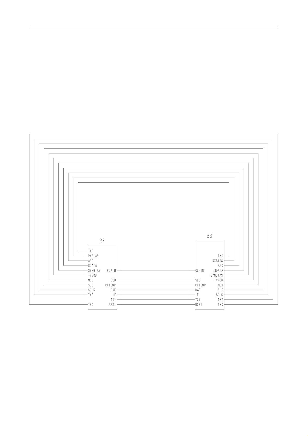
Connections between RF and BB Sections (Version: 6.0 Edit: 42) Page 4–24. .
Block Diagram of Baseband Page 4–25. . . . . . . . . . . . . . . . . . . . . . . . . . . . . .
Block Diagram of NASTA Page 4–26. . . . . . . . . . . . . . . . . . . . . . . . . . . . . . . .
Block Diagram of MUUMI Page 4–27. . . . . . . . . . . . . . . . . . . . . . . . . . . . . . . .
Block Diagram of Baseband Power Distribution Page 4–28. . . . . . . . . . . . .
JR4: Circuit Diagram of Baseband Section (Version:12 Edit:134) Page 4–29. . .
Page 4–2
Original 06/97
Page 3

After Sales
NHA–2
Technical Documentation
JR4: Circuit Diagram of Baseband Section (Version:13 Edit:140) Page 4–30. . .
JR4: Circuit Diagram of MCU & EEPROM (Version:12 Edit: 95) Page 4–31
JR4: Circuit Diagram of MCU & EEPROM (Version:13 Edit: 99) Page 4–32
JR4: Circuit Diagram of Audio (Version:12 Edit: 144) Page 4–33. . . . . . . .
JR4: Circuit Diagram of Audio (Version:13 Edit:159) Page 4–34. . . . . . . . .
JR4: Circuit Diagram of Power Supply (Version:12 Edit:128) Page 4–35. .
JR4: Circuit Diagram of Power Supply (Version:13 Edit:129) Page 4–36. .
JR4: Circuit Diagram of User Interface (Version:12 Edit: 89) Page 4–37. .
JR4: Circuit Diagram of User Interface (Version:13 Edit:89) Page 4–38. . .
Block Diagram of RF Section Page 4–39. . . . . . . . . . . . . . . . . . . . . . . . . . . . .
Power Distribution Diagram of RF Section Page 4–40. . . . . . . . . . . . . . . . . .
JR4: Circuit Diagram of RF Section (version 12) Page 4–41. . . . . . . . . . . .
JR4: Circuit Diagram of RF Section (version 13) Page 4–42. . . . . . . . . . . .
System Module
JR7: Circuit Diagram of RF Section (version 13) Page 4–43. . . . . . . . . . . .
JR4: Layout Diagrams (version 12) Page 4–44. . . . . . . . . . . . . . . . . . . . . . . .
JR4: Layout Diagrams (version 13) Page 4–45. . . . . . . . . . . . . . . . . . . . . . . .
JR7: Layout Diagrams (version 13) Page 4–46. . . . . . . . . . . . . . . . . . . . . . . .
JR7: Circuit Diagram of Baseband Section (Version:13 Edit:140) Page 4–47. . .
JR7: Circuit Diagram of MCU & EEPROM (Version:13 Edit: 98) Page 4–48
JR7: Circuit Diagram of Audio (Version:13 Edit: 159) Page 4–49. . . . . . . .
JR7: Circuit Diagram of Power Supply (Version:13 Edit:129) Page 4–50. .
JR7: Circuit Diagram of User Interface (Version:13 Edit: 89) Page 4–51. .
Part List of JR4 (Code: 0200613, Issue: 9.12) Page 4–52. . . . . . . . . . . . . .
Part List of JR4 (Code: 0200613, Issue: 13.0) Page 4–65. . . . . . . . . . . . . .
Part List of JR7 (Code: 0200843, EDMS Issue:13.0 ) Page 4–74. . . . . . . .
Original 06/97
Page 4–3
Page 4

NHA–2
After Sales
System Module
Introduction
System module is designed to operate in handportable phone in AMPS system.
Baseband hardware is integrated to same printed circuit board with RF hard-
ware. Module includes modem, audio filters, microcontroller, power supply, non-
volatile memory, keyboard and display. Display is a different module. The mo-
dem and audio operations is integrated to NASTA ASIC. Power supply circuits
like regulators, voltage detection and charging control are integrated to custom
MUUMI circuit. The microcontroller is a Hitachi H8 series controller with mini-
mum 60–64 kbytes ROM and 2 kbytes RAM. The 2 kbyte nonvolatile EEPROM
memory is a serial IIC–bus type device. This custom EEPROM includes also 16
bytes one time programmable (OTP) part for electrical serial number (ESN)
The display is a 5*7 dot matrix, 2 line liquid crystal display with single chip con-
troller IC with negative voltage generation for LCD and RF VCOs.
Technical Specifications
Technical Documentation
Modes of Operation
The system module hardware module has 4 basic operation modes: active
(call), standby (service) and power off.
Page 4–4
Original 06/97
Page 5

After Sales
NHA–2
Technical Documentation
External and Internal Connections
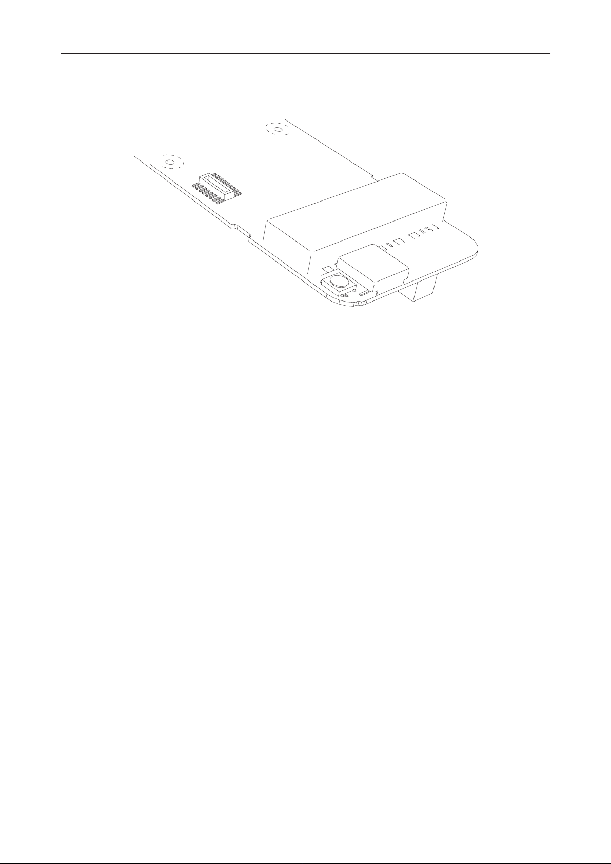
The system module has two connector, external bottom connector and internal
display module connector.
Bottom Connector
14
13
15
System Module
16
S0001130
Accessory Connector
Pin: Name: Description:
1 GND Digital ground
2 V_OUT Battery voltage out
3 XMIC External microphone input and accessory
4 NC No connection
5 NC No connection
6 MBUS Bidirectional asynchronous bus
7 NC No connection
7
12
17 20
16
• min/typ/max: 3.25...4...6 V (load 3 mA)
identification
• min/max: 0...VA+1.0 V
• logic low level: 0...05 V
• logic high level: 2.4...3.5 V
1918
8 SGND Signal ground
9 XEAR External audio output and mute control
Original 06/97
• mute on: 0...0.5 V d.c.
• mute off: 1.0...2.0 V d.c.
Page 4–5
Page 6

NHA–2
After Sales
System Module
Pin: Name: Description:
10 HOOK Hook control, accessory connection detect
11 NC No connection
12 VIN Charging voltage input
Battery Connector
Pin: Name: Description:
13 GND Battery ground
14 BSI Battery size indicator
15 BTEM Battery temperature
Technical Documentation
• hook off (handset in use) : 0...05 V
• hook on, (handset not in use): 2.4...3.5 V
• max: 16 V
• R2=47k pullup resistor in
module
• 47 kΩ NTC in battery to gnd,
47 kΩ pullup in module
16 VBAT Battery voltage
Charging connectors
Pin: Name: Description:
17, 19 VC Charging voltage input
18, 20 GND Charger ground
• min/typ/max: 4.0...4.8...8.0 V
• min/max: 4...16 V
Page 4–6
Original 06/97
Page 7
After Sales
NHA–2
Technical Documentation
Display Connector
1
S0001113
Pin: Name: Description:
1, 15 VBAT Battery voltage
System Module
9
16
8
• voltage min/typ/max: 4.2...4.8...6.8 V
• illumination current typ/max: 20...40 mA
2 LIGHTS Display illumination control
• lights on voltage typ/max: 1.4...1.75 V
• drive current typ/max: 100...200 µA
3 LCDCLK Display controller clock input
• 80 kHz/0...3.5 V
4, 16 GND Ground
5 –VOUT Negative voltage out
• voltage min/typ/max: –6.0...–6.6...–7.0 V
• max load current: 50 µA
6 VL Supply voltage to controller
• voltage min/typ/max: 3.1...3.3...3.5 V
• loading current typ/max: 1.4...1.5 mA
7 _RESET Controller reset input
• low/high voltage: 0.6 V/2.8 V
8 RS Register select
• low/high voltage: 0.6 V/2.8 V
9 R/W Read/write select
• low/high voltage: 0.6 V/2.8 V
10 E Enable controller bus
11–14 DB0–DB3 Controller 4–bit data bus, DB4=MSB
Original 06/97
• low/high voltage: 0.6 V/2.8 V
• low/high voltage: 0.6 V/2.8 V
Page 4–7
Page 8

NHA–2
After Sales
System Module
Baseband Block Description
Circuit Description
The module consists of following main components:
– H8/3042 16–bit single chip microcontroller with 64 kbytes ROM (EPROM)
and 2 kbytes RAM
– NASTA modem and audio ASIC
– External audio amplifier with on/off control and buzzer driver circuit
– MUUMI power supply (and control), ASIC and discrete charge switch control
logic
– serial I2C–bus 2 kbytes EEPROM with 16 bytes one time programmable
electrical serial number (ESN) area
– NJU6428 LCD controller with 2* VL negative voltage generation is located in
the separate display module
The baseband block diagram illustrates the baseband module connections and
interface to charger, battery and display module.
Technical Documentation
Microcontroller
NHA–2 microcontroller is a H8/3042, that is operating in single–chip normal
mode (mode 6) 64 kbyte address space. Maximum 62 kbytes ROM can be
used for program. MCU operating clock (=2.4 MHz) is generated on NASTA.
Microcontroller includes 2 serial channels, 5 pcs 16–bit timer units(ITU) with
PWM and interval capability, 10–bit A/D–converter with 8 channels, watchdog
timer and refresh timer. Serial channel 0 is used for asynchronous M2BUS–
communication and channel 1 is used for synchronous synthesizer interface.
Four timer units are used for pulse width modulation (PWM) outputs: buzzer
control(BUZZ_DRIVE) ITU0, charge control (CSWPWM) ITU1, TX power control (TXC) ITU2 and TX booster power control (BENA) ITU3. M2BUS net free
interrupt reserves one timer unit ITU4. Keyboard interface reserves 10
I/O–lines: 4 column outputs (COL3–0) and 6 row inputs. Different power on/off
switch is connected through MUUMI circuit to MCU input PWRON.
Page 4–8
Original 06/97
Page 9

After Sales
NHA–2
Technical Documentation
Input/Output Ports of MCU
All input/output pins are used as I/O–ports. NASTA address and data bus is
connected to I/O–pins.
Port 1
Pin name Pin use description
P10/A0 NA0, NASTA address bus ,output
P11/A1 NA1, NASTA address bus ,output
P12/A2 NA2, NASTA address bus ,output
P13/A3 NA3, NASTA address bus ,output
P14/A4 NCS
P15/A5 NRD, NASTA read control output
P16/A6 NWR, NASTA write control output
P17/A7
Port 2
Pin name Pin use description
System Module
, NASTA chip select control output
Port 3
P20/A8 ROW0, Keyboard matrix row input 0 (input pullup used)
P21/A9 ROW1, Keyboard matrix row input 1 (input pullup used)
P22/A10 ROW2, Keyboard matrix row input 2 (input pullup used)
P23/A11 ROW3, Keyboard matrix row input 3 (input pullup used)
P24/A12 ROW4, Keyboard matrix row input 4 (input pullup used)
P25/A13 ROW5, Keyboard matrix row input 5 (input pullup used)
P26/A14 PWRON, buffered power on key input (=1 when PWR–
key pressed)
P27/A15 LIGHTS, Keyboard and display illumination on/off=1/0
control output
Pin name Pin use description
P30/D8 ND0, NASTA data bus,I/O
P31/D9 ND1, NASTA data bus,I/O
P32/D10 ND2, NASTA data bus,I/O
P33/D11 ND3, NASTA data bus,I/O
P34/D12 ND4, NASTA data bus,I/O
P35/D13 ND5, NASTA data bus,I/O
P36/D14 ND6, NASTA data bus,I/O
P37/D15 ND7, NASTA data bus,I/O
Original 06/97
Page 4–9
Page 10

NHA–2
After Sales
System Module
Port 4
Pin name Pin use description
P40/D0 SLE, Synthesizer latch enable
P41/D1 unused output
P42/D2 TXE, Transmitter regulator on/off=1/0 control
P43/D3 TXS, Transmitter synthesizer on/off control
P44/D4 RXV0, RX VCO aligning output
P45/D5 RXV1, RX VCO aligning output
P46/D6 RXV2, RX VCO aligning output
P47/D7 SLD, synthesizer lock detect input, internal pullup used
Port 5
Pin name Pin use description
P50/A16 COL0, Keyboard column output 0
P51/A17 COL1, Keyboard column output 1
P52/A18 COL2, Keyboard column output 2
P53/A19 COL3, Keyboard column output 3
Technical Documentation
(pullup used, when input)
(pullup used, when input)
(pullup used ,when input)
(pullup used ,when input)
Port 6
Pin name Pin use description
P60/WAIT DB0, LCD controller data bus,I/O
P61/BREQ DB1, LCD controller data bus,I/O
P62/BACK
P63/AS DB3, LCD controller data bus,I/O
P64/RD E, LCD controller bus enable control output
P65/HWR
P66/LWR RS, LCD controller register select control output
DB2, LCD controller data bus,I/O
R/W, LCD controller bus read/write control output
Page 4–10
Original 06/97
Page 11

After Sales
NHA–2
Technical Documentation
Port 7
Pin name Pin use description
P70/AN0 VBSW, Battery (VBAT) voltage measurement input
P71/AN1 VCSW, Charger voltage measurement input
P72/AN2 BSI, Battery size indication
P73/AN3 BTEMP, Battery temperature measurement
P74/AN4 RSSI, Receiver Signal Strenght Indication
P75/AN5 TXI, Transmitter power indication
P76/AN6 RFTEMP, RF temperature measurement
P77/AN7 XMIC, external audio and accessory identification input
Port 8
Pin name Pin use description
System Module
(10–bit resolution)
HEADSET ADAPTER connected: 602 nominal
(685...505 accepted), Compact HF connected:
410 nominal (504...324 accepted )
Port 9
P80/RFS/IRQ0 NINT, Interrupt from NASTA
P81/CS3
P82/CS2
P83/CS1/IRQ3 unused output
P84/CS0
Pin name Pin use description
P90/TxD0 MBUS out
P91/TxD1 SDATA,Synthesizer serial data output
P92/RxD0 MBUS in
P93/RxD1 SDA, serial EEPROM IIC–bus data
P94/SCK0/IRQ4
P95/SCK1/IRQ5 SCLK, serial data clock output to synthesizers
/IRQ1 HOOK, HOOK on=1/off=0 status, accessory
connect interrupt (falling edge)
/IRQ2 EXT_RF, 0=external antenna in use, input
(not used in C1, configure as output)
unused output
SCL, serial EEPROM IIC–bus clock
Original 06/97
Page 4–11
Page 12

NHA–2
After Sales
System Module
Port A
Pin name Pin use description
PA0 XEARON, external audio amplifier on/off=1/0 and hands
PA1/TCLKB LCDCLK, 80 kHz clock input for slow clock PWM to timer
PA2/TIOCA0 BUZZ_DRIVE, Buzzer drive output from timer unit 0, level
PA3/TIOCB0 unused output
PA4/TIOCA1 CSWPWM, Charger PWM control output (Timer unit 1)
PA5/TIOCB1 XPWROFF, Power off and watchdog clear control output,
PA6/TIOCA2 TXC, Transmitter power control PWM output (Timer unit 2)
PA7/TIOCB2 RXV3, RX VCO aligning output
Port B
Pin name Pin use description
Technical Documentation
free mute (on=0) control
unit 1
adjust with PWM
watchdog cleared on falling edge
PB0/TP8/TIOCA3 BENA, TX booster power control PWM output
(not used in C1 product)
PB1/TP9/TIOCB3 ABC/PWR key input, =0 when ABC/PWR key pressed
PB2/TP10/TIOCA4 unused output
PB3/TP11/TIOCB4 MBUSNF, MBUS net free timer input (Timer unit 4)
PB4/TP12/TOCXA4 unused output
PB5/TP13/TOCXB4 unused output
PB6/TP14 unused output
PB7/TP15 unused output
Page 4–12
Original 06/97
Page 13

After Sales
NHA–2
Technical Documentation
A/D Converter of MCU
A/D converter has 10 bit resolution with ±8 LSB absolute accuracy and 3.3 V
±3% reference voltage input. All 8 analog inputs can be multiplexed to A/D con-
verter input. The A/D conversion time is 134 CPU clock cycles maximum
(CKS=1) and input sampling time is 40 clock cycles.
Description of Input Channels
Channel 0: WBSW, Battery Voltage Measurement
Battery voltage can be measured from 4 V to 9.075 V nominal with 3.3 V reference voltage. The absolute accuracy is low because of the reference 3 % accuracy and A/D converter ±8 LSB accuracy. This battery voltage measurement
offset error must be calibrated with input voltage 4.8 V. The A/D conversion result can be calculated from equation:
A/D readout = 1024 * (VBSW* ( 4/11))/VREF VREF=3.3 V
For example (voltage, min/nom/max A/D value):
4.3 V 456...484...515 cutt off limit/idle
4.8 V 509...541...575 battery voltage reference trim
6.8 V 722...767...815 high battery charging voltage limit
System Module
Channel 1: VCSW, Charger Voltage Measurement
Charger voltage can be measured up to 21.6 V nominal. The A/D conversion
result can be calculated from equation:
A/D readout = 1024 * (VCSW*(18/118))/VREF VREF=3.3 V
For example:
4.8 V 198...227...257 Charger voltage reference trim
10 V 413...473...536 –
11 V 661...757...859 Max charger voltage
Channel 2: BSI, Battery Size Indication
Battery capacity can be defined with BSI resistor value calculated from equation:
BSI = 47 kΩ / ((4 mAh * 1023)/ C) –1)
A/D readout gives battery capacity from equation:
A/D readout = C/4 C= Battery capacity
For example:
470 mAh/6.8 kΩ 121...129...137
950 mAh/15 kΩ 235...247...261
1.2 Ah/20 kΩ 291...305...321
1.6 Ah/30 kΩ 382...398...416
Original 06/97
Page 4–13
Page 14

NHA–2
After Sales
System Module
Channel 3: BTEMP, Battery Temperature Measurement
Battery temperature measurement is implemented with 47 kΩ NTC and 47 kΩ
pullup resistor. The A/D conversion readout can be calculated from equation:
A/D readout= 1024* ( R
NTC
/( R
NTC
+47kΩ))
For example:
5 °C 705...743...780
25 °C 486...512...537
45 °C 289...305...320
Channel 4: RSSI, Receive Signal Strength
Receiving signal strength is proportional to input voltage / A/D–readout.
Typical value for noise level signal strength is 0.2 V = 0062= 03E H and for
maximum signal strength is 2.4 V = 0744 = 2E8 H. Input value for –90 dBm RF
input level is typically 1.16 V= 0360 = 168 H . RF input level change of 1 dBm
equals about 24 mV= 7.5 A/D steps.
Channel 5: TXI, Transmitter Power Level Indication
Transmitter power level indication is used to monitor the transmitted power level. A/D input is used to check, if TX power is on or off. The limit for check is
1.0 V, which is equal to 320 as A/D readout.
Technical Documentation
Channel 6: RFTEMP, RF VCXO Temperature Measure
VCXO module temperature measurement is based on CMOS temperature sensor chip with linear – 8.1 mV/K voltage output. The nominal output voltage of
sensor IC is at +30 °C 1.497 V. One degree temperature change is equal to 2.5
A/D quantisize steps.
For example:
–20 °C 549...589...636
+30 °C 429...464...508
+80 °C 304...336...376
Channel 7: ID, Accessory Identification Input
Accessory identification is included in XMIC signal d.c. voltage level = ID analog input. This d.c. voltage level is defined by pullup resistor. Compact HF unit
and headset adapter can be recognized from this input:
Compact HF unit 324...409...504 22 kΩ pulldown resistor
Headset adapter 505...601...685 47 kΩ pulldown resistor
LCD controller interface to microcontroller is a 4–bit parallel type including 4 bidirectional data lines DB3–0 (port 63–60), register select control RS (port 66)
output, read/write control R/W (port 65) output and bus enable control E (port
64) output. Data lines DB3–0 and control signals RS ,R/W must be set to high
state during standby operation because of the pullup resistors in LCD controller. LCD controller resetting requires clock during _RESET active low . This
clock is created with LCD controller internal RC–oscillator changing LCDCLK
output from NASTA to 3–state.
Page 4–14
Original 06/97
Page 15

After Sales
NHA–2
Technical Documentation
Interface between microcontroller and NASTA circuit is bidirectional 8–bit parallel type with 4 address lines. Address, data and control lines are used in microcontroller as I/O–port pins. Data lines direction must be controlled with microcontroller data direction register. Interface includes address outputs NA3–0
(port 1), data inputs (read) / outputs (write) ND7–0 (port 3), chip select control
output NCS
NWR (port 16) and interrupt input NINT (port 80) . If NASTA circuit is not selected , control signals (read,write and chip select) must be in high state and
data lines must be outputs.
The serial I2C–bus interface EEPROM is connected to MCU I/O–pins:
SDA (serial data) to port 93 and SCL (serial clock) to port 94.
MCU SLEEP Mode Operation
Microcontroller is driven to sleep mode by software in order to save power. In
sleep mode all I/O–pins,RAM and CPU registers are held. Timers, clock and
supporting functions are active. MCU exits from sleep mode by interrupt: NASTA modem interrupt, MBUS serial communication interface interrupt (SCI 0) or
operating system timer interrupt (refresh controller timer).
(port 14), read control output NRD (port 15) , write control output
System Module
Audio
The main audio and modem operations are included in NASTA ASIC circuit.
NASTA includes following operations:
– AMPS/TACS modem with extended standby operation
– all RX/TX audio filters, compander, limiters, mute switches
– microphone amplifier, ceramic earpiece amplifier, accessory audio output
(XEAR) and input (XMIC).
– DTMF generator.
– IF counter and 8–bit D/A–output for AFC control
– voltage controlled oscillator and clock generation
The NASTA circuit is connected to MCU with 8–bit parallel bus and interrupt request line.
The 14.85 MHz clock input is generated in RF module voltage controlled crystal
oscillator (VCXO). This input clock is used to synthesize 4.8 MHz clock to NASTA internal circuits. NASTA creates 2.4 MHz clock to microcontroller
(CLKMCU) and 80 kHz clock to LCD controller. The buzzer driver amplifier is
driven by MCU PWM output. The buzzer volume level is adjusted with pulse
width. The accessory audio output line XEAR is driven by transistor pair (V53)
buffer. The buffer is short circuit protected with 47 ohm series resistor and has
on/off (mute) control from MCU output (XEARON). This XEAR buffer amplifier
outputs more than 1.6 V DC voltage to control accessory audio to mute off
state. Accessory audio input XMIC is connected also with low pass filter (R52
and C70) to MCU A/D–converter input. This accessory identification input (ID)
is used to recognize the connected accessory type and check, if accessory is
connected or not.
Original 06/97
Page 4–15
Page 16

NHA–2
After Sales
System Module
NASTA RX Signal Paths
The incoming audio, data and SAT (Supervisory Audio Tone) analog signal
(DAF = N2 pin 27) is connected through the RX trimmer and the anti alias filter
to modem data comparator input, to 6 kHz bandpass type SAT filter input and
to receive audio filter.
The data from the anti alias filter is connected through the comparator to a
Manchester decoder, which decodes Manchester data to the NRZ (Non Return
to Zero) format.Modem is synchronized to the receiving data with a digital
phase locked loop and a word synchronization detection block. Data validity is
continuously detected, and this information is used internally when word synchronization detection is accepted.The serial data from the Manchester decoder is 3/5 majority voted, BCH–decoded, corrected and shifted to receiver register. The Receiver timing block extracts the data from received frames on control
and voice channels and generates data transfer interrupts . It maintains bit and
word synchronization during different frames and passes the synchronization
status forward to the status register.
The SAT signal is filtered and amplified with a bandpass filter . Signal is converted to digital square wave signal with a comparator .SAT detection is done
with a digital PLL/detection circuitry. The regenerated SAT is then fed to transmit summing block.
Technical Documentation
RX audio signal is selected with the input mux. Other possibilities is to select
DTMF or RX mute. RX audio signal is filtered with a de–emphasis and bandpass filter. Signal is fed through amplitude expander 1:2 (EXP). RX volume level is controlled with amplifier in the range –20 ... +17.5 dB.Hands free control
block includes a bandpass filter, window comparator and controller for RX TX
attenuators. RX hands free attenuator has selectable minimum gain from
–30...–21 dB to max 0 dB. RX and TX attenuation sum is always constant at HF
use (30...21 dB). Side tone is added to earphone signal. The audio signal is fed
either to earphone amplifier output (EARM, EARP) or to accessory audio amplifier output (XEAR).
NASTA TX Signal Paths
The data to be transmitted will be loaded into the transmitting data register.
From the transmit data register the 8 bit data is transformed to serial data which
is fed to the Manchester encoder and then to the summing block output (MOD,
N2 pin 55).
Microphone signal is fed to microphone amplifier input (MIC, N2 pin 43). NASTA has a control for microphone bias current output (BIMIC, N2 pin 44). Signal
source can be selected with the input multiplexer: microphone, accessory input
(XMIC, N2 pin 46) or internal dtmf generator. TX hands free attenuator has selectable minimum gain from –30...–21 dB to maximum 0 dB. Signal is going to
trimmer, which is tuned for nominal speech deviation or DTMF level. Signal is
filtered in the TX audio bandpass filter.
Page 4–16
Original 06/97
Page 17

After Sales
NHA–2
Technical Documentation
Signal is fed through amplitude compressor 2:1 to the first limiter for low frequency amplitude limiting. Signal is then pre–emphasised and limited again.
Signal is lowpass filtered and fed to trimmer for speech maximum deviation tuning. It is fed to the TX summing block to be summed with data, ST and SAT
signals.
DTMF generator generates dual and single tones for RX and TX lines. Tolerance of DTMF frequencies is ±1.5 %.
User Interface
The user interface includes interface to display module and keyboard with illumination. The display module is connected with 16 pin connector. The display
module interface includes 4 bit data bus (DB(3:0)), bus enable (E), read/write
(R_W), register select (RS), reset (_RESET) and 80 kHz clock input to LCD–
controller (LCDCLK). The keyboard illumination includes 12 LEDs and 2 transistor(V42, V43) drivers. Keyboard consists of 6*4 matrix and different ABC/
PWR–key and PWR–switch. The keyboard interface to microcontroller includes
4 column outputs from MCU (COL(3:0)), 6 row inputs (ROW(5:0)), ABC/PWR–
key input (ABCKEY) and PWR–switch input (PWRON).
System Module
Power
Module goes to power on state always, when either ABC/PWR–key or PWR
switch is pressed. The software decides, if ABC/PWR–key is active power key
or not. This and other key variations is defined by software.
The baseband power supplying circuit MUUMI includes:
– 3 pcs 3.3 V regulated outputs
– VL = Logic voltage for digital circuits
– VA = Analog voltage for analog circuits
– VREF = Reference voltage for A/D converter and RF regulator
– switched outputs of battery (VBSW) and charger voltage (VCSW)
measurement to MCU A/D–converter
– battery voltage detection and reset logic
– charger switch control output used to limit battery voltage VBAT < 8.0V
– power on/off switch input (XPWRON), buffered output to MCU (PWRON)
– watchdog timer using oscillator in COFF pin, cleared by falling edge input in
PWROFFX, elapsing time for WD timer is 1...3 seconds
– M2BUS open drain output driver
The charge switch driving circuit is implemented with discrete components. This
circuit includes transient voltage protection, soft charge switching, low voltage
battery charging and battery disconnecting with charger connected protection.
This circuit also limits battery voltage when charger is connected to protect
MUUMI and TX transistors.
Original 06/97
Page 4–17
Page 18

NHA–2
After Sales
System Module
Power Circuit Operation
NHA–2 power circuitry have three different operating modes: POWER OFF,
RESET and POWER ON. In POWER OFF state MUUMI regulator outputs are
disabled and reset control output signal (PURX) is active low. MUUMI internal
oscillator at pin COFF is working in all operating modes. MUUMI goes through
short RESET state (100 ms) to POWER ON–state, if PWR–button is pressed or
charger voltage input is connected to charging input VC (charging voltage
detection in MUUMI input VCHAR is level active). In RESET–state regulator
outputs VL, VA and VREF are active and PURX–signal is active low. If battery
voltage VBAT is lower than 4.1 V (3.9 V...4.3 V) the circuit cannot go to POWER
ON state. MUUMI goes also to RESET state, when battery voltage is falling below 3.9 V (3.7 V...4.1 V). This situation is possible, when battery is fully discharged or battery is disconnected.
In POWER ON mode all regulator outputs are active and MUUMI reset signal
output PURX is inactive high. Microcontroller XPWROFF–output signal clears
at falling edge the watchdog inside MUUMI. If the watchdog is not cleared,
MUUMI goes to POWER OFF state. When the charger is connected and battery voltage is higher than 4.1 V, module stays in POWER ON mode.
Technical Documentation
The microcontroller controls battery charging with CSWPWM output and
MUUMI limits the maximum battery voltage to 7.6 V with CHRGSW–output.
No current flows from charger (VC) to battery, if MCU output CSWPWM is active low and _RESET signal is inactive high. The battery is charged also, when
charger is connected and _RESET signal is active low. The charging circuit
charges the battery during RESET to higher than 4.3 V
Page 4–18
Original 06/97
Page 19

After Sales
NHA–2
Technical Documentation
MBUS Hardware Description
MBUS hardware interface consists of serial communication interface channel
inside MCU, net free timer (MCU), open drain output driver (MUUMI), 4.7 kΩ
pull–up resistor and protection/filtering resistor/capasitors. MBUS voltage levels
are based to 3.3 V supply voltage.
N1 (MUUMI)
M2BUSIN
11
asychronous data
output from MCU
(pin 12)
760k
M2BUSOUT
12
System Module
received data input to
MCU(pin 14) and net
free timer input to MCU
(pin 5)
Bidirectional MBUS
signal to system
connector
ESN Description
The Electrical Serial Number can be programmed only once and cannot be manipulated in the field. The custom EEPROM circuit includes 16 bytes one time
programmable (OTP) part for the ESN. The ESN component is a SO–8 package soldered to main printed circuit board.
The software of the microcontroller is not alterable and cannot even be read,
because of the microcontroller security option. The microcontroller program
memory is either OTP or mask type.
Original 06/97
Page 4–19
Page 20

NHA–2
After Sales
System Module
RF Block Description
Receiver
The receiver is a dual–conversion superheterodyne using two intermediate frequencies, 45 MHz and 450 kHz.
The RF signal from the duplexer RX port is applied to the RF amplifier. The amplifier is realized with transistor V700. Amplifier stage input matching is accomplished by C701. R700 and R701 are used for biasing. Output matching is carried out by Z03 and Z04. Components C702 and C703 are used for RF
bypassing. The RF amplifier and the IF circuit are connected in series with
R702 so that the same supply current is passed through both stages.
Next the signal is filtered with Z703. The filter is followed by a single balanced
diode mixer, realized with Z701, Z711, Z712, C709, C716 and V701.
After the mixer the 45 MHz IF signal is filtered with crystal filter Z702. The
matching between mixer and the filter is realized with L706 and C706. Next the
IF signal is amplified by V703. Input matching is realized with C714, L702 and
L705. The biasing is realized with R713, R714 and R710. From the amplifier
the IF–signal is applied to the second mixer.
Technical Documentation
The second mixer, the LO buffer transistor, IF amplifier and quadrature detector
are all integrated in the circuit N700. The second LO frequency, 44.55 MHz, is
third harmonic off the VCXO frequency. LO signal is realized with tank circuit
C719 and L710. After the mixer the 450 kHz IF signal is filtered with ceramic
filter Z704. Between the filter and IF amplifier is a band–pass filter consisting of
C728, L709 and C730. The IF amplifier output signal is phase shifted by resonance circuit C727, C723, R712 and L704. After this the signal is fed to a quadrature detector.
Signal DAF is low pass filtered by R716 and C734. The DAF, RSSI and 2nd IF
signal (450 kHz) are fed to the audio/logic unit.
RX Synthesizer
The first injection frequency is generated by a digital phase locked loop (PLL).
The output frequency of the loop (LO) is obtained from a voltage–controlled oscillator (VCO) V602. The bandwidth of the PLL can be varied by dataword programming. The VCO output signal is amplified by transistor V601 and fed to the
receiver mixer via Z06. The injection level required by the receiver mixer is
about +3 dBm. In addition, the signal is fed to the dualsynthesizer circuit N650
and via R625 to a LO amplifier which is realized with V661.
Page 4–20
The overall divisor of the chain is selected according to the desired channel.
The internal dividers of N650 are programmed with 17 bits, which are trans-
ferred serially on the SDATA (synthesizer data) line from the processor into an
internal shift register also locating in N650. Data transfer is timed with SCLK
clock pulses.
Original 06/97
Page 21

After Sales
NHA–2
Technical Documentation
The divided frequency is compared with a highly stable reference frequency by
a phase comparator in the PLL circuit (N650). The phase comparator controls
the VCO frequency by means of a d.c. voltage through the loop filter so as to
keep the divided frequency applied to the phase comparator equal to the fixed
reference frequency.
The reference frequency is 30 kHz. This reference frequency is obtained from
The voltage controlled crystal oscillator (VCXO). The oscillator frequency is
14.85 MHz. The VCXO frequency is divided by 495.
RX Loop Filter
Phase comparator output is pin 3. If the VCO frequency is too high, the output
goes low and discharge integrating capacitor C618. After this, the DC control
voltage and the VCO frequency will decrease.
If the VCO frequency is too low, the output goes high and charge the integrating capacitor C618. Thereafter the DC control voltage and the VCO frequency
will go up.
Output pulses from the phase detector have to be supplied to the loop filter.
The function of the integrator is to convert positive and negative pulses to DC
voltage. The remaining ripple and AC components are filtered in the lowpass
filter. The integrator comprises components R610, C619, C624 and C618. The
lowpass filter consists of R608 and C616.
System Module
RX VCO
The VCO is a Clapp type oscillator. The oscillator’s resonant frequency is determined by the circuitry Z600, C604, V603,C601, C614, C611, C612 and C613.
The center frequency of the VCO is adjusted by changing amount of constant
current generated by V100 in BB section. The VCO signal is amplified by buffer
amplifier V601. This amplifier produces a level of –5 dBm to the synthesizer
N650 and amplifier V661 in TX synthesizer via R625. The same buffer V601
produces +3 dBm level to the first mixer via Z06.
TX Synthesizer
The transmitter synthesizer generates a frequency modulated transmitter signal
for the transmitter section.
The TX offset synthesizer consists of a 90 MHz PLL circuit, passive loop filter
and a 90 MHz VCO equipped with a chip coil resonator. The bandwidth of the
PLL can be varied by dataword programming. Modulation is brought to the
VCO.
The TX signal is obtained by mixing the signals of offset synthesizer and RX
synthesizer with a single balanced diode mixer. From the mixer the –10 dBm
level is fed to the amplifier. The TX signal is filtered with a SAW filter before inputting it to the transmitter.
Original 06/97
Page 4–21
Page 22

NHA–2
After Sales
System Module
TX VCO
The VCO is a Clapp type oscillator. The oscillator’s resonance frequency is determined by the circuitry L651, C659, V659, C663, C630, C631 and C675. The
center frequency of the resonance circuit is not adjustable (By increasing or decreasing the capacitor C659 the resonance frequency can be changed). The
VCO signal is amplified by V657 and fed to the prescaler and to the mixer.
TX Loop Filter
Output pulses from the phase detector N650 pin 17 have to be supplied to the
loop filter. The integrator, which is constituted of R674, C680 and C683, converts positive and negative pulses to d.c. voltage. The remaining ripple is filtered in the low–pass filter accomplished by R672 and C665.
Transmitter
The transmitter is realized with four discrete transistors. The modulated RF signal from the TX synthesizer is applied to the input transistor V660 of the transmitter. V660 amplifies the signal for the power control stage V803, which is
biased to B–class. The power level is controlled by the collector voltage of
V803. Transistors V804 and V805 are biased to C–class and amplify the RF
signal to the desired output power level. The amplified RF signal is fed through
a low–pass filter to the duplex filter. The harmonics of the transmitter are reduced by the duplex filter. A voltage proportional to the output power is rectified
from a directional coupler by d.c. biased Schottky diode V801. This rectified
voltage is fed to a differential amplifier which consists of double transistor V809.
There is a negative feedback from the rectified voltage to the bias voltage of
diode V801 consisting of transistor V810 and associated components. The purpose of arranging the feedback is to suppress the rectified voltage to a range
below 3 volts. The reference voltage is filtered from the PWM signal TXC by
R814 and C826. The differential amplifier adjusts the collector voltage of the
transistor V803 so that the reference voltage and the voltage proportional to the
output power are equal. The transmitter is switched on when TXE goes high
(logic 1), which enables the transmitter power control circuit by transistor V808
and the first stage of the transmitter. When the transmitter is inactive (TXE low)
the RF level from the transmitter is reduced below –60 dBm.
Technical Documentation
Page 4–22
The rectified voltage, which is proportional to the power output signal, is fed
along TXI line through R820 to the BB–unit. This TXI line (TX power on Indicator) is used to avoid false transmission.
Original 06/97
Page 23

After Sales
NHA–2
Technical Documentation
Regulators
Transistors V901 and V902 form a voltage regulator for RF parts. It is realized
with discrete transistors because the output noise has to be very low. The 3.3 V
reference voltage (VREF) comes from the logic module. This regulated voltage
goes directly to RX part and also to RX synthesizer. TX synthesizer get it’s supply voltage via a switch. The switch is realized with transistors V651 and
V654.It is controlled over digital line TXS from the logic module.
System Module
Original 06/97
Page 4–23
Page 24
NHA–2
After Sales
System Module
Technical Documentation
Connections between RF and BB Sections (Version: 6.0 Edit: 42)
Page 4–24
Original 06/97
Page 25
After Sales
NHA–2
Technical Documentation
Block Diagram of Baseband
NASTA
DAF
D/A
IF
CTR
SPEECH
DATA/ST
CLK
DIV
SYNBIAS
RXBIAS
14.85 MHz
MOD
AFC
IF
CTR
CLK
GEN
SAT
DATA
SAT
DET
MAN
DPLL
DEC
MCU INTERFACE
ND0–7,NA0–3
_NCS,_WR,_RD
_NINT
HF
DET
VOTE
SMUX
SMUX
DATA/
ST
ENCODE
System Module
EARPHONE
EAR
XEARON
XMIC
BUZZ_DRIVE
VBAT
XEAR
MIC
MICROPHONE
BUZZER
VC
4.8V
NTC
Battery
pack
–VMOD
TXE,TXS,TXC
SLE,SDATA,SCLK
Charge
switch
control
VBAT
BTEMP
BSI
ON/OFF
VCO
NEG VOLT
TRIM
–VLCD
XEARON
RXV(3:0)
RF CONTROLS
HOOK, EXT_RF
Charger
det,crl
VB det
RESET
PWR ON
WDOG
MUUMI
VBSW
VCSW
BTEMP
BSI
RSSI
TXI
RFTEMP
XMIC/ID
RESET,PWRON
MBUS
2.4MHz
WDOG
TIMER
ITU
16 BIT
TIMERS
INTERRUPT
CONTROL
A/D
10 BIT
8 CH
TXD,XPWROFF
VL=3.3V
VA=3.3V
VREF=3.3V
H8/3042
H8/300
CPU
ROM
64K
RAM
2K
SCL,SDA
EEPROM
2 kbytes
VCSW
VBSW
DMA
REFRESH
CONTRL
TPC,
TIMING
PATTERN CRL
SCI
SERIAL
IFCE
2 CHAN
80 kHz
RS,R/W,E,
DB0–3
LIGHTS
ROW0–5
COM1–7,COM9–15,COMMK
SEG1–60
LCD–
CONTROLLER
KEYBOARD
COL0–3
HOOK
EXT_RF
XEAR
XMIC
ACCESSORY
CONNECTOR
–VLCDout
MBUS
HOOK
EXT_RF
XEAR
XMIC
BENA
V_OUT
Original 06/97
Page 4–25
Page 26

Page 4–26
MIC
BIMIC
CMIC
XMIC
50
REF
2.4
MICAM
DTMF GEN
GND GEN
14.85 MHz>500 pp
CLKIN
CLKOUT
OSC
IFAMP
IF
(450 kHz)
REF GEN
CLKGEN
TXMUX TXATT MICTRI TXBP
XCLR
TMODE
CLKLCD CLKMCU
TSEL
CLOCKDIV
MCS1&2
IFCNTR
MANDEC
Nom–dev
50 71
ATTO
COMI
CWCI
COMO
COMPR LIM1
sideari
BCH
INT
CLOCKS
VOTE
TIMER
EMPI
SMUX
CORR
100
EMPO LPIN
PREEM LIM2 TXLP TXTRI
MANEN
STATUS BITS
TR
Par/Ser
SYNBIAS
CONTROL BITS
RXBIAS
TOUT
CREG
Max–dev
aloop
DATA
GEN
SAT
GEN
ST
GEN
SUM
TXTRI
SATFIL
HFBP
SATCOMP
DATAC
CAMPBO
Extended
210
Data–dev
WTRFIL
ATST
ATOUT
D/St 1640 pp
Sat 410/435 pp
210
MOD
loop
Block Diagram of NASTA
System Module
NHA–2
VDD1
VDD2
VSS2
VDA1
VSA1
VDA2
VSA2
VSS1
DAF
50
D 398 pp
Sat 99/100 pp
Original 06/97
DATAC
D 792 pp
dtmf
RXTRI RXAAF
100
DPLL
loop
DATVAL
RXMUX
aloop
XCSXRDXWRXINT A0 A1 A2 A3 D0 D1 D2 D3 D4 D5 D6 D7
SATFIL,6kHz SATCOMP SATDET
360
RXFIL
71
FILO
EXP VOL
EAMPBO
EXPI
EWCI
EXPO
4
VOLI
50
INTERFACE
HF
CONTR
RXATT ACC
Level: AMPS/TACS (mVrms)
All levels: (mV)
( ) : Not use now
EAR
64 pins Tqfp
50
EARP
50
EARM
EVGND
XEAR
50
VDD1
XRD
XCS
A3
A2
A1
A0
D7
D6
D5
D4
D3
D2
D1
D0
VDD2
1 2 3 4 5 6 7 8 9 10111213141516
63CLKMCU
64XWR
18 XCLR
17 TOUT
61CLKIN
62CLKLCD
20 TSEL
19 TMODE
59ATOUT
60CLKOUT
22 SYNBIAS
21 XINT
57VSS1
58BUZZ
NASTA
24 IF
23 RXBIAS
56VSA1
25 VSS2
55MOD
26 VSA2
sideari
SIDEAR
AFC
dtmf
D/A
8 bit
BUZZ DRIV
DACO
BUZZ
Technical Documentation
(1500 pp)
(3000 pp)
49COMI
50COMO
51EMPI
52EMPO
53LPIN
54ATST
48474645444342414039383736353433
VDA1
ATTO
XMIC
CMIC
BIMIC
MIC
REF
SIDEAR
DACO
CWCI
EARP
EARM
EVGND
XEAR
VOLI
VDA2
32 EXPO
31 EWCI
30 EAMPBO
29 EXPI
28 FILO
27 DAF
After Sales
Page 27

After Sales
NHA–2
Technical Documentation
Block Diagram of MUUMI
VBAT1
1
VBAT2
22
VBAT3
5
M2BUSIN
11
760k
BANDGAP
REF
PWM
15
760k
CHARGER
CTRL
LOGIC
70k
40k
System Module
VBATSW
M2BUSOUT
VREF
17
12
VL
23
VA
2
4
21
13
14
3
VCHAR
PWRONX
PWROFFX
TEST
VBAT
32k
760k
760k
LOW VBAT
& CHARGER
DETECT
PWR ON/OFF
&
RESET LOGIC
Creset
20
16
Coff
VL_ENA
VA_ENA
VREF_ENA
VSW_ENA
VCHAR
24
GND1
GND2
19
GND3
7
CHRGSW
PWRONXBUFF
VCHARSW
Cref
6
PURX
8
10
9
18
Original 06/97
Page 4–27
Page 28

NHA–2
After Sales
System Module
Technical Documentation
Block Diagram of Baseband Power Distribution
VC
VB
MUUMI
VL
VREF
VA
NASTA
EEPROM
Microcontroller
LCD
controller
Page 4–28
Original 06/97
Page 29

After Sales
NHA–2
Technical Documentation
System Module
JR4: Circuit Diagram of Baseband Section (Version:12 Edit:134)
Original 06/97
Page 4–29
Page 30

NHA–2
After Sales
System Module
Technical Documentation
JR4: Circuit Diagram of Baseband Section (Version:13 Edit:140)
Page 4–30
Original 06/97
Page 31

After Sales
NHA–2
Technical Documentation
System Module
JR4: Circuit Diagram of MCU & EEPROM (Version:12 Edit: 95)
Original 06/97
Page 4–31
Page 32

NHA–2
After Sales
System Module
Technical Documentation
JR4: Circuit Diagram of MCU & EEPROM (Version:13 Edit: 99)
Page 4–32
Original 06/97
Page 33

After Sales
NHA–2
Technical Documentation
JR4: Circuit Diagram of Audio (Version:12 Edit: 144)
System Module
Original 06/97
Page 4–33
Page 34

NHA–2
After Sales
System Module
Technical Documentation
JR4: Circuit Diagram of Audio (Version:13 Edit:159)
Page 4–34
Original 06/97
Page 35

After Sales
NHA–2
Technical Documentation
System Module
JR4: Circuit Diagram of Power Supply (Version:12 Edit:128)
Original 06/97
Page 4–35
Page 36

NHA–2
After Sales
System Module
Technical Documentation
JR4: Circuit Diagram of Power Supply (Version:13 Edit:129)
Page 4–36
Original 06/97
Page 37

After Sales
NHA–2
Technical Documentation
System Module
JR4: Circuit Diagram of User Interface (Version:12 Edit: 89)
Original 06/97
Page 4–37
Page 38

NHA–2
After Sales
System Module
Technical Documentation
JR4: Circuit Diagram of User Interface (Version:13 Edit:89)
Page 4–38
Original 06/97
Page 39

After Sales
NHA–2
Technical Documentation
Block Diagram of RF Section
System Module
Original 06/97
Page 4–39
Page 40

NHA–2
After Sales
System Module
Technical Documentation
Power Distribution Diagram of RF Section
Page 4–40
Original 06/97
Page 41

After Sales
NHA–2
Technical Documentation
JR4: Circuit Diagram of RF Section (version 12)
System Module
Original 06/97
Page 4–41
Page 42

NHA–2
After Sales
System Module
Technical Documentation
JR4: Circuit Diagram of RF Section (version 13)
Page 4–42
Original 06/97
Page 43

After Sales
NHA–2
Technical Documentation
JR7: Circuit Diagram of RF Section (version 13)
System Module
Original 06/97
Page 4–43
Page 44

NHA–2
After Sales
System Module
JR4: Layout Diagrams (version 12)
Technical Documentation
Page 4–44
Original 06/97
Page 45

After Sales
NHA–2
Technical Documentation
JR4: Layout Diagrams (version 13)
System Module
Original 06/97
Page 4–45
Page 46

NHA–2
After Sales
System Module
JR7: Layout Diagrams (version 13)
Technical Documentation
Page 4–46
Original 06/97
Page 47

After Sales
NHA–2
Technical Documentation
System Module
JR7: Circuit Diagram of Baseband Section (Version:13 Edit:140)
Original 06/97
Page 4–47
Page 48

NHA–2
After Sales
System Module
Technical Documentation
JR7: Circuit Diagram of MCU & EEPROM (Version:13 Edit: 98)
Page 4–48
Original 06/97
Page 49

After Sales
NHA–2
Technical Documentation
JR7: Circuit Diagram of Audio (Version:13 Edit: 159)
System Module
Original 06/97
Page 4–49
Page 50

NHA–2
After Sales
System Module
Technical Documentation
JR7: Circuit Diagram of Power Supply (Version:13 Edit:129)
Page 4–50
Original 06/97
Page 51

After Sales
NHA–2
Technical Documentation
System Module
JR7: Circuit Diagram of User Interface (Version:13 Edit: 89)
Original 06/97
Page 4–51
Page 52

NHA–2
After Sales
System Module
Technical Documentation
Part List of JR4 (Code: 0200613, Issue: 9.12)
ITEM CODE DESCRIPTION VALUE TYPE
R001 1430770 Chip resistor 4.7 k 5 % 0.063 W 0402
R002 1430796 Chip resistor 47 k 5 % 0.063 W 0402
R003 1430796 Chip resistor 47 k 5 % 0.063 W 0402
R004 1430796 Chip resistor 47 k 5 % 0.063 W 0402
R005 1430778 Chip resistor 10 k 5 % 0.063 W 0402
R006 1430778 Chip resistor 10 k 5 % 0.063 W 0402
R007 1430804 Chip resistor 100 k 5 % 0.063 W 0402
R008 1430796 Chip resistor 47 k 5 % 0.063 W 0402
R009 1430796 Chip resistor 47 k 5 % 0.063 W 0402
R011 1430790 Chip resistor 27 k 5 % 0.063 W 0402
R014 1430830 Chip resistor 1.0 M 5 % 0.063 W 0402
R015 1430796 Chip resistor 47 k 5 % 0.063 W 0402
R016 1430758 Chip resistor 1.5 k 5 % 0.063 W 0402
R017 1430740 Chip resistor 330 5 % 0.063 W 0402
R018 1430764 Chip resistor 3.3 k 5 % 0.063 W 0402
R019 1430788 Chip resistor 22 k 5 % 0.063 W 0402
R020 1430770 Chip resistor 4.7 k 5 % 0.063 W 0402
R021 1430778 Chip resistor 10 k 5 % 0.063 W 0402
R022 1430780 Chip resistor 12 k 5 % 0.063 W 0402
R023 1430786 Chip resistor 18 k 5 % 0.063 W 0402
R024 1430778 Chip resistor 10 k 5 % 0.063 W 0402
R025 1430730 Chip resistor 150 5 % 0.063 W 0402
R026 1430804 Chip resistor 100 k 5 % 0.063 W 0402
R027 1430786 Chip resistor 18 k 5 % 0.063 W 0402
R028 1430770 Chip resistor 4.7 k 5 % 0.063 W 0402
R029 1430770 Chip resistor 4.7 k 5 % 0.063 W 0402
R030 1430734 Chip resistor 220 5 % 0.063 W 0402
R031 1430754 Chip resistor 1.0 k 5 % 0.063 W 0402
R032 1430754 Chip resistor 1.0 k 5 % 0.063 W 0402
R033 1430754 Chip resistor 1.0 k 5 % 0.063 W 0402
R034 1430754 Chip resistor 1.0 k 5 % 0.063 W 0402
R035 1430804 Chip resistor 100 k 5 % 0.063 W 0402
R036 1430778 Chip resistor 10 k 5 % 0.063 W 0402
R040 1430762 Chip resistor 2.2 k 5 % 0.063 W 0402
R041 1430762 Chip resistor 2.2 k 5 % 0.063 W 0402
R042 1430710 Chip resistor 22 5 % 0.063 W 0402
R043 1430710 Chip resistor 22 5 % 0.063 W 0402
R044 1430754 Chip resistor 1.0 k 5 % 0.063 W 0402
R045 1430778 Chip resistor 10 k 5 % 0.063 W 0402
R050 1430792 Chip resistor 33 k 5 % 0.063 W 0402
R051 1430762 Chip resistor 2.2 k 5 % 0.063 W 0402
R052 1430778 Chip resistor 10 k 5 % 0.063 W 0402
R053 1430762 Chip resistor 2.2 k 5 % 0.063 W 0402
Page 4–52
Original 06/97
Page 53

After Sales
NHA–2
Technical Documentation
R054 1430804 Chip resistor 100 k 5 % 0.063 W 0402
R056 1430764 Chip resistor 3.3 k 5 % 0.063 W 0402
R058 1430710 Chip resistor 22 5 % 0.063 W 0402
R059 1430710 Chip resistor 22 5 % 0.063 W 0402
R060 1430778 Chip resistor 10 k 5 % 0.063 W 0402
R061 1430816 Chip resistor 330 k 5 % 0.063 W 0402
R062 1430788 Chip resistor 22 k 5 % 0.063 W 0402
R063 1430710 Chip resistor 22 5 % 0.063 W 0402
R064 1430700 Chip resistor 10 5 % 0.063 W 0402
R065 1430744 Chip resistor 470 5 % 0.063 W 0402
R066 1430718 Chip resistor 47 5 % 0.063 W 0402
R067 1430744 Chip resistor 470 5 % 0.063 W 0402
R071 1430804 Chip resistor 100 k 5 % 0.063 W 0402
R072 1430804 Chip resistor 100 k 5 % 0.063 W 0402
R073 1430804 Chip resistor 100 k 5 % 0.063 W 0402
R100 1430812 Chip resistor 220 k 5 % 0.063 W 0402
R101 1430816 Chip resistor 330 k 5 % 0.063 W 0402
R102 1430822 Chip resistor 560 k 5 % 0.063 W 0402
R103 1430830 Chip resistor 1.0 M 5 % 0.063 W 0402
R104 1430826 Chip resistor 680 k 5 % 0.063 W 0402
R106 1430808 Chip resistor 150 k 5 % 0.063 W 0402
R107 1430790 Chip resistor 27 k 5 % 0.063 W 0402
R600 1430726 Chip resistor 100 5 % 0.063 W 0402
R601 1430804 Chip resistor 100 k 5 % 0.063 W 0402
R602 1430804 Chip resistor 100 k 5 % 0.063 W 0402
R604 1430710 Chip resistor 22 5 % 0.063 W 0402
R605 1430832 Chip resistor 2.7 k 5 % 0.063 W 0402
R606 1430724 Chip resistor 82 5 % 0.063 W 0402
R607 1430726 Chip resistor 100 5 % 0.063 W 0402
R608 1430776 Chip resistor 8.2 k 5 % 0.063 W 0402
R609 1430720 Chip resistor 56 5 % 0.063 W 0402
R610 1430762 Chip resistor 2.2 k 5 % 0.063 W 0402
R611 1430762 Chip resistor 2.2 k 5 % 0.063 W 0402
R612 1430764 Chip resistor 3.3 k 5 % 0.063 W 0402
R613 1430728 Chip resistor 120 5 % 0.063 W 0402
R614 1430718 Chip resistor 47 5 % 0.063 W 0402
R615 1430798 Chip resistor 56 k 5 % 0.063 W 0402
R616 1430700 Chip resistor 10 5 % 0.063 W 0402
R617 1430746 Chip resistor 560 5 % 0.063 W 0402
R619 1430774 Chip resistor 6.8 k 5 % 0.063 W 0402
R620 1430796 Chip resistor 47 k 5 % 0.063 W 0402
R621 1430778 Chip resistor 10 k 5 % 0.063 W 0402
R622 1430778 Chip resistor 10 k 5 % 0.063 W 0402
R623 1430778 Chip resistor 10 k 5 % 0.063 W 0402
R624 1430718 Chip resistor 47 5 % 0.063 W 0402
R625 1430722 Chip resistor 68 5 % 0.063 W 0402
R626 1430832 Chip resistor 2.7 k 5 % 0.063 W 0402
R627 1430762 Chip resistor 2.2 k 5 % 0.063 W 0402
System Module
Original 06/97
Page 4–53
Page 54

NHA–2
After Sales
System Module
R628 1430700 Chip resistor 10 5 % 0.063 W 0402
R629 1430832 Chip resistor 2.7 k 5 % 0.063 W 0402
R630 1430832 Chip resistor 2.7 k 5 % 0.063 W 0402
R631 1430710 Chip resistor 22 5 % 0.063 W 0402
R632 1430804 Chip resistor 100 k 5 % 0.063 W 0402
R633 1430740 Chip resistor 330 5 % 0.063 W 0402
R635 1430714 Chip resistor 33 5 % 0.063 W 0402
R636 1430754 Chip resistor 1.0 k 5 % 0.063 W 0402
R637 1430714 Chip resistor 33 5 % 0.063 W 0402
R639 1430742 Chip resistor 390 5 % 0.063 W 0402
R640 1430778 Chip resistor 10 k 5 % 0.063 W 0402
R641 1430726 Chip resistor 100 5 % 0.063 W 0402
R644 1430788 Chip resistor 22 k 5 % 0.063 W 0402
R645 1430700 Chip resistor 10 5 % 0.063 W 0402
R646 1430710 Chip resistor 22 5 % 0.063 W 0402
R647 1430710 Chip resistor 22 5 % 0.063 W 0402
R652 1430778 Chip resistor 10 k 5 % 0.063 W 0402
R653 1430764 Chip resistor 3.3 k 5 % 0.063 W 0402
R654 1430804 Chip resistor 100 k 5 % 0.063 W 0402
R656 1430762 Chip resistor 2.2 k 5 % 0.063 W 0402
R659 1430754 Chip resistor 1.0 k 5 % 0.063 W 0402
R660 1430700 Chip resistor 10 5 % 0.063 W 0402
R663 1430722 Chip resistor 68 5 % 0.063 W 0402
R664 1430754 Chip resistor 1.0 k 5 % 0.063 W 0402
R667 1430748 Chip resistor 680 5 % 0.063 W 0402
R668 1430718 Chip resistor 47 5 % 0.063 W 0402
R669 1430778 Chip resistor 10 k 5 % 0.063 W 0402
R670 1430742 Chip resistor 390 5 % 0.063 W 0402
R671 1430754 Chip resistor 1.0 k 5 % 0.063 W 0402
R672 1430764 Chip resistor 3.3 k 5 % 0.063 W 0402
R673 1430764 Chip resistor 3.3 k 5 % 0.063 W 0402
R674 1430762 Chip resistor 2.2 k 5 % 0.063 W 0402
R675 1430700 Chip resistor 10 5 % 0.063 W 0402
R681 1430726 Chip resistor 100 5 % 0.063 W 0402
R683 1430802 Chip resistor 82 k 5 % 0.063 W 0402
R700 1430778 Chip resistor 10 k 5 % 0.063 W 0402
R701 1430754 Chip resistor 1.0 k 5 % 0.063 W 0402
R702 1430700 Chip resistor 10 5 % 0.063 W 0402
R703 1430754 Chip resistor 1.0 k 5 % 0.063 W 0402
R705 1430726 Chip resistor 100 5 % 0.063 W 0402
R710 1430774 Chip resistor 6.8 k 5 % 0.063 W 0402
R712 1430764 Chip resistor 3.3 k 5 % 0.063 W 0402
R713 1430784 Chip resistor 15 k 5 % 0.063 W 0402
R714 1430754 Chip resistor 1.0 k 5 % 0.063 W 0402
R715 1430758 Chip resistor 1.5 k 5 % 0.063 W 0402
R716 1430762 Chip resistor 2.2 k 5 % 0.063 W 0402
R717 1430700 Chip resistor 10 5 % 0.063 W 0402
R718 1430700 Chip resistor 10 5 % 0.063 W 0402
Technical Documentation
Page 4–54
Original 06/97
Page 55

After Sales
NHA–2
Technical Documentation
R721 1430724 Chip resistor 82 5 % 0.063 W 0402
R801 1430724 Chip resistor 82 5 % 0.063 W 0402
R804 1430734 Chip resistor 220 5 % 0.063 W 0402
R805 1430762 Chip resistor 2.2 k 5 % 0.063 W 0402
R806 1430746 Chip resistor 560 5 % 0.063 W 0402
R807 1430700 Chip resistor 10 5 % 0.063 W 0402
R808 1430718 Chip resistor 47 5 % 0.063 W 0402
R809 1430700 Chip resistor 10 5 % 0.063 W 0402
R810 1430718 Chip resistor 47 5 % 0.063 W 0402
R811 1430700 Chip resistor 10 5 % 0.063 W 0402
R813 1430700 Chip resistor 10 5 % 0.063 W 0402
R814 1430778 Chip resistor 10 k 5 % 0.063 W 0402
R815 1430778 Chip resistor 10 k 5 % 0.063 W 0402
R816 1430792 Chip resistor 33 k 5 % 0.063 W 0402
R817 1430754 Chip resistor 1.0 k 5 % 0.063 W 0402
R818 1430792 Chip resistor 33 k 5 % 0.063 W 0402
R819 1430770 Chip resistor 4.7 k 5 % 0.063 W 0402
R820 1430792 Chip resistor 33 k 5 % 0.063 W 0402
R821 1430772 Chip resistor 5.6 k 5 % 0.063 W 0402
R823 1430804 Chip resistor 100 k 5 % 0.063 W 0402
R824 1430770 Chip resistor 4.7 k 5 % 0.063 W 0402
R825 1430710 Chip resistor 22 5 % 0.063 W 0402
R901 1430762 Chip resistor 2.2 k 5 % 0.063 W 0402
R902 1430788 Chip resistor 22 k 5 % 0.063 W 0402
R903 1430754 Chip resistor 1.0 k 5 % 0.063 W 0402
R904 1430778 Chip resistor 10 k 5 % 0.063 W 0402
R906 1430778 Chip resistor 10 k 5 % 0.063 W 0402
C001 2320107 Ceramic cap. 10 n 5 % 50 V 0603
C002 2320107 Ceramic cap. 10 n 5 % 50 V 0603
C003 2320107 Ceramic cap. 10 n 5 % 50 V 0603
C004 2320107 Ceramic cap. 10 n 5 % 50 V 0603
C005 2320107 Ceramic cap. 10 n 5 % 50 V 0603
C006 2320107 Ceramic cap. 10 n 5 % 50 V 0603
C007 2320107 Ceramic cap. 10 n 5 % 50 V 0603
C008 2320107 Ceramic cap. 10 n 5 % 50 V 0603
C009 2320107 Ceramic cap. 10 n 5 % 50 V 0603
C011 2320107 Ceramic cap. 10 n 5 % 50 V 0603
C012 2310784 Ceramic cap. 100 n 10 % 25 V 0805
C013 2320544 Ceramic cap. 22 p 5 % 50 V 0402
C015 2320107 Ceramic cap. 10 n 5 % 50 V 0603
C016 2320107 Ceramic cap. 10 n 5 % 50 V 0603
C017 2610100 Tantalum cap. 1R001 1430770 Chip resistor
4.7 k 5 % 0.063 W 0402
R002 1430796 Chip resistor 47 k 5 % 0.063 W 0402
R003 1430796 Chip resistor 47 k 5 % 0.063 W 0402
R004 1430796 Chip resistor 47 k 5 % 0.063 W 0402
R005 1430778 Chip resistor 10 k 5 % 0.063 W 0402
R006 1430778 Chip resistor 10 k 5 % 0.063 W 0402
System Module
Original 06/97
Page 4–55
Page 56

NHA–2
After Sales
System Module
R007 1430804 Chip resistor 100 k 5 % 0.063 W 0402
R008 1430796 Chip resistor 47 k 5 % 0.063 W 0402
R009 1430796 Chip resistor 47 k 5 % 0.063 W 0402
R011 1430790 Chip resistor 27 k 5 % 0.063 W 0402
R014 1430830 Chip resistor 1.0 M 5 % 0.063 W 0402
R015 1430796 Chip resistor 47 k 5 % 0.063 W 0402
R016 1430758 Chip resistor 1.5 k 5 % 0.063 W 0402
R017 1430740 Chip resistor 330 5 % 0.063 W 0402
R018 1430764 Chip resistor 3.3 k 5 % 0.063 W 0402
R019 1430788 Chip resistor 22 k 5 % 0.063 W 0402
R020 1430770 Chip resistor 4.7 k 5 % 0.063 W 0402
R021 1430778 Chip resistor 10 k 5 % 0.063 W 0402
R022 1430780 Chip resistor 12 k 5 % 0.063 W 0402
R023 1430786 Chip resistor 18 k 5 % 0.063 W 0402
R024 1430778 Chip resistor 10 k 5 % 0.063 W 0402
R025 1430730 Chip resistor 150 5 % 0.063 W 0402
R026 1430804 Chip resistor 100 k 5 % 0.063 W 0402
R027 1430786 Chip resistor 18 k 5 % 0.063 W 0402
R028 1430770 Chip resistor 4.7 k 5 % 0.063 W 0402
R029 1430770 Chip resistor 4.7 k 5 % 0.063 W 0402
R030 1430734 Chip resistor 220 5 % 0.063 W 0402
R031 1430754 Chip resistor 1.0 k 5 % 0.063 W 0402
R032 1430754 Chip resistor 1.0 k 5 % 0.063 W 0402
R033 1430754 Chip resistor 1.0 k 5 % 0.063 W 0402
R034 1430754 Chip resistor 1.0 k 5 % 0.063 W 0402
R035 1430804 Chip resistor 100 k 5 % 0.063 W 0402
R036 1430778 Chip resistor 10 k 5 % 0.063 W 0402
R040 1430762 Chip resistor 2.2 k 5 % 0.063 W 0402
R041 1430762 Chip resistor 2.2 k 5 % 0.063 W 0402
R042 1430710 Chip resistor 22 5 % 0.063 W 0402
R043 1430710 Chip resistor 22 5 % 0.063 W 0402
R044 1430754 Chip resistor 1.0 k 5 % 0.063 W 0402
R045 1430778 Chip resistor 10 k 5 % 0.063 W 0402
R050 1430792 Chip resistor 33 k 5 % 0.063 W 0402
R051 1430762 Chip resistor 2.2 k 5 % 0.063 W 0402
R052 1430778 Chip resistor 10 k 5 % 0.063 W 0402
R053 1430762 Chip resistor 2.2 k 5 % 0.063 W 0402
R054 1430804 Chip resistor 100 k 5 % 0.063 W 0402
R056 1430764 Chip resistor 3.3 k 5 % 0.063 W 0402
R058 1430710 Chip resistor 22 5 % 0.063 W 0402
R059 1430710 Chip resistor 22 5 % 0.063 W 0402
R060 1430778 Chip resistor 10 k 5 % 0.063 W 0402
R061 1430816 Chip resistor 330 k 5 % 0.063 W 0402
R062 1430788 Chip resistor 22 k 5 % 0.063 W 0402
R063 1430710 Chip resistor 22 5 % 0.063 W 0402
R064 1430700 Chip resistor 10 5 % 0.063 W 0402
R065 1430744 Chip resistor 470 5 % 0.063 W 0402
R066 1430718 Chip resistor 47 5 % 0.063 W 0402
Technical Documentation
Page 4–56
Original 06/97
Page 57

After Sales
NHA–2
Technical Documentation
R067 1430744 Chip resistor 470 5 % 0.063 W 0402
R071 1430804 Chip resistor 100 k 5 % 0.063 W 0402
R072 1430804 Chip resistor 100 k 5 % 0.063 W 0402
R073 1430804 Chip resistor 100 k 5 % 0.063 W 0402
R100 1430812 Chip resistor 220 k 5 % 0.063 W 0402
R101 1430816 Chip resistor 330 k 5 % 0.063 W 0402
R102 1430822 Chip resistor 560 k 5 % 0.063 W 0402
R103 1430830 Chip resistor 1.0 M 5 % 0.063 W 0402
R104 1430826 Chip resistor 680 k 5 % 0.063 W 0402
R106 1430808 Chip resistor 150 k 5 % 0.063 W 0402
R107 1430790 Chip resistor 27 k 5 % 0.063 W 0402
R600 1430726 Chip resistor 100 5 % 0.063 W 0402
R601 1430804 Chip resistor 100 k 5 % 0.063 W 0402
R602 1430804 Chip resistor 100 k 5 % 0.063 W 0402
R604 1430710 Chip resistor 22 5 % 0.063 W 0402
R605 1430832 Chip resistor 2.7 k 5 % 0.063 W 0402
R606 1430724 Chip resistor 82 5 % 0.063 W 0402
R607 1430726 Chip resistor 100 5 % 0.063 W 0402
R608 1430776 Chip resistor 8.2 k 5 % 0.063 W 0402
R609 1430720 Chip resistor 56 5 % 0.063 W 0402
R610 1430762 Chip resistor 2.2 k 5 % 0.063 W 0402
R611 1430762 Chip resistor 2.2 k 5 % 0.063 W 0402
R612 1430764 Chip resistor 3.3 k 5 % 0.063 W 0402
R613 1430728 Chip resistor 120 5 % 0.063 W 0402
R614 1430718 Chip resistor 47 5 % 0.063 W 0402
R615 1430798 Chip resistor 56 k 5 % 0.063 W 0402
R616 1430700 Chip resistor 10 5 % 0.063 W 0402
R617 1430746 Chip resistor 560 5 % 0.063 W 0402
R619 1430774 Chip resistor 6.8 k 5 % 0.063 W 0402
R620 1430796 Chip resistor 47 k 5 % 0.063 W 0402
R621 1430778 Chip resistor 10 k 5 % 0.063 W 0402
R622 1430778 Chip resistor 10 k 5 % 0.063 W 0402
R623 1430778 Chip resistor 10 k 5 % 0.063 W 0402
R624 1430718 Chip resistor 47 5 % 0.063 W 0402
R625 1430722 Chip resistor 68 5 % 0.063 W 0402
R626 1430832 Chip resistor 2.7 k 5 % 0.063 W 0402
R627 1430762 Chip resistor 2.2 k 5 % 0.063 W 0402
R628 1430700 Chip resistor 10 5 % 0.063 W 0402
R629 1430832 Chip resistor 2.7 k 5 % 0.063 W 0402
R630 1430832 Chip resistor 2.7 k 5 % 0.063 W 0402
R631 1430710 Chip resistor 22 5 % 0.063 W 0402
R632 1430804 Chip resistor 100 k 5 % 0.063 W 0402
R633 1430740 Chip resistor 330 5 % 0.063 W 0402
R635 1430714 Shipres 0w06 33r j 0402 0402
R636 1430754 Chip resistor 1.0 k 5 % 0.063 W 0402
R637 1430714 Shipres 0w06 33r j 0402 0402
R639 1430742 Chip resistor 390 5 % 0.063 W 0402
R640 1430778 Chip resistor 10 k 5 % 0.063 W 0402
System Module
Original 06/97
Page 4–57
Page 58

NHA–2
After Sales
System Module
R641 1430726 Chip resistor 100 5 % 0.063 W 0402
R644 1430788 Chip resistor 22 k 5 % 0.063 W 0402
R645 1430700 Chip resistor 10 5 % 0.063 W 0402
R646 1430710 Chip resistor 22 5 % 0.063 W 0402
R647 1430710 Chip resistor 22 5 % 0.063 W 0402
R652 1430778 Chip resistor 10 k 5 % 0.063 W 0402
R653 1430764 Chip resistor 3.3 k 5 % 0.063 W 0402
R654 1430804 Chip resistor 100 k 5 % 0.063 W 0402
R656 1430762 Chip resistor 2.2 k 5 % 0.063 W 0402
R659 1430754 Chip resistor 1.0 k 5 % 0.063 W 0402
R660 1430700 Chip resistor 10 5 % 0.063 W 0402
R663 1430722 Chip resistor 68 5 % 0.063 W 0402
R664 1430754 Chip resistor 1.0 k 5 % 0.063 W 0402
R667 1430748 Chip resistor 680 5 % 0.063 W 0402
R668 1430718 Chip resistor 47 5 % 0.063 W 0402
R669 1430778 Chip resistor 10 k 5 % 0.063 W 0402
R670 1430742 Chip resistor 390 5 % 0.063 W 0402
R671 1430754 Chip resistor 1.0 k 5 % 0.063 W 0402
R672 1430764 Chip resistor 3.3 k 5 % 0.063 W 0402
R673 1430764 Chip resistor 3.3 k 5 % 0.063 W 0402
R674 1430762 Chip resistor 2.2 k 5 % 0.063 W 0402
R675 1430700 Chip resistor 10 5 % 0.063 W 0402
R681 1430726 Chip resistor 100 5 % 0.063 W 0402
R683 1430802 Chip resistor 82 k 5 % 0.063 W 0402
R700 1430778 Chip resistor 10 k 5 % 0.063 W 0402
R701 1430754 Chip resistor 1.0 k 5 % 0.063 W 0402
R702 1430700 Chip resistor 10 5 % 0.063 W 0402
R703 1430754 Chip resistor 1.0 k 5 % 0.063 W 0402
R705 1430726 Chip resistor 100 5 % 0.063 W 0402
R710 1430774 Chip resistor 6.8 k 5 % 0.063 W 0402
R712 1430764 Chip resistor 3.3 k 5 % 0.063 W 0402
R713 1430784 Chip resistor 15 k 5 % 0.063 W 0402
R714 1430754 Chip resistor 1.0 k 5 % 0.063 W 0402
R715 1430758 Chip resistor 1.5 k 5 % 0.063 W 0402
R716 1430762 Chip resistor 2.2 k 5 % 0.063 W 0402
R717 1430700 Chip resistor 10 5 % 0.063 W 0402
R718 1430700 Chip resistor 10 5 % 0.063 W 0402
R721 1430724 Chip resistor 82 5 % 0.063 W 0402
R801 1430724 Chip resistor 82 5 % 0.063 W 0402
R804 1430734 Chip resistor 220 5 % 0.063 W 0402
R805 1430762 Chip resistor 2.2 k 5 % 0.063 W 0402
R806 1430746 Chip resistor 560 5 % 0.063 W 0402
R807 1430700 Chip resistor 10 5 % 0.063 W 0402
R808 1430718 Chip resistor 47 5 % 0.063 W 0402
R809 1430700 Chip resistor 10 5 % 0.063 W 0402
R810 1430718 Chip resistor 47 5 % 0.063 W 0402
R811 1430700 Chip resistor 10 5 % 0.063 W 0402
R813 1430700 Chip resistor 10 5 % 0.063 W 0402
Technical Documentation
Page 4–58
Original 06/97
Page 59

After Sales
NHA–2
Technical Documentation
R814 1430778 Chip resistor 10 k 5 % 0.063 W 0402
R815 1430778 Chip resistor 10 k 5 % 0.063 W 0402
R816 1430792 Chip resistor 33 k 5 % 0.063 W 0402
R817 1430754 Chip resistor 1.0 k 5 % 0.063 W 0402
R818 1430792 Chip resistor 33 k 5 % 0.063 W 0402
R819 1430770 Chip resistor 4.7 k 5 % 0.063 W 0402
R820 1430792 Chip resistor 33 k 5 % 0.063 W 0402
R821 1430772 Chip resistor 5.6 k 5 % 0.063 W 0402
R823 1430804 Chip resistor 100 k 5 % 0.063 W 0402
R824 1430770 Chip resistor 4.7 k 5 % 0.063 W 0402
R825 1430710 Chip resistor 22 5 % 0.063 W 0402
R901 1430762 Chip resistor 2.2 k 5 % 0.063 W 0402
R902 1430788 Chip resistor 22 k 5 % 0.063 W 0402
R903 1430754 Chip resistor 1.0 k 5 % 0.063 W 0402
R904 1430778 Chip resistor 10 k 5 % 0.063 W 0402
R906 1430778 Chip resistor 10 k 5 % 0.063 W 0402
C001 2320107 Ceramic cap. 10 n 5 % 50 V 0603
C002 2320107 Ceramic cap. 10 n 5 % 50 V 0603
C003 2320107 Ceramic cap. 10 n 5 % 50 V 0603
C004 2320107 Ceramic cap. 10 n 5 % 50 V 0603
C005 2320107 Ceramic cap. 10 n 5 % 50 V 0603
C006 2320107 Ceramic cap. 10 n 5 % 50 V 0603
C007 2320107 Ceramic cap. 10 n 5 % 50 V 0603
C008 2320107 Ceramic cap. 10 n 5 % 50 V 0603
C009 2320107 Ceramic cap. 10 n 5 % 50 V 0603
C011 2320107 Ceramic cap. 10 n 5 % 50 V 0603
C012 2310784 Ceramic cap. 100 n 10 % 25 V 0805
C013 2320544 Ceramic cap. 22 p 5 % 50 V 0402
C015 2320107 Ceramic cap. 10 n 5 % 50 V 0603
C016 2320107 Ceramic cap. 10 n 5 % 50 V 0603
C017 2610100 Tantalum cap. 1 u 20 % 10 V 2.0x1.3x1.2
C018 2604456 Tantalum cap. 4.7 u 20 % 16 V 4.7x2.6x2.1
C019 2320107 Ceramic cap. 10 n 5 % 50 V 0603
C020 2320107 Ceramic cap. 10 n 5 % 50 V 0603
C021 2320107 Ceramic cap. 10 n 5 % 50 V 0603
C022 2604199 Tantalum cap. 2.2 u 20 % 3.2x1.6x1.6
C023 2604199 Tantalum cap. 2.2 u 20 % 3.2x1.6x1.6
C024 2604199 Tantalum cap. 2.2 u 20 % 3.2x1.6x1.6
C025 2320576 Ceramic cap. 470 p 5 % 50 V 0402
C030 2320546 Ceramic cap. 27 p 5 % 50 V 0402
C050 2310791 Ceramic cap. 33 n 20 % 50 V 0805
C051 2310791 Ceramic cap. 33 n 20 % 50 V 0805
C052 2310791 Ceramic cap. 33 n 20 % 50 V 0805
C053 2310791 Ceramic cap. 33 n 20 % 50 V 0805
C054 2310791 Ceramic cap. 33 n 20 % 50 V 0805
C055 2310784 Ceramic cap. 100 n 10 % 25 V 0805
C056 2310791 Ceramic cap. 33 n 20 % 50 V 0805
C057 2310777 Ceramic cap. 22 n 20 % 50 V 0805
System Module
Original 06/97
Page 4–59
Page 60

NHA–2
After Sales
System Module
C058 2320546 Ceramic cap. 27 p 5 % 50 V 0402
C059 2320107 Ceramic cap. 10 n 5 % 50 V 0603
C060 2320107 Ceramic cap. 10 n 5 % 50 V 0603
C062 2310791 Ceramic cap. 33 n 20 % 50 V 0805
C063 2310791 Ceramic cap. 33 n 20 % 50 V 0805
C064 2310791 Ceramic cap. 33 n 20 % 50 V 0805
C066 2312410 Ceramic cap. 1.0 u 10 % 16 V 1206
C068 2320107 Ceramic cap. 10 n 5 % 50 V 0603
C069 2320584 Ceramic cap. 1.0 n 5 % 50 V 0402
C070 2312410 Ceramic cap. 1.0 u 10 % 16 V 1206
C071 2320546 Ceramic cap. 27 p 5 % 50 V 0402
C072 2320546 Ceramic cap. 27 p 5 % 50 V 0402
C076 2310784 Ceramic cap. 100 n 10 % 25 V 0805
C077 2320584 Ceramic cap. 1.0 n 5 % 50 V 0402
C600 2320520 Ceramic cap. 2.2 p 0.25 % 50 V 0402
C601 2320526 Ceramic cap. 3.9 p 0.25 % 50 V 0402
C602 2320524 Ceramic cap. 3.3 p 0.25 % 50 V 0402
C603 2320560 Ceramic cap. 100 p 5 % 50 V 0402
C604 2320546 Ceramic cap. 27 p 5 % 50 V 0402
C605 2611668 Tantalum cap. 4.7 u 20 % 10 V 3.2x1.6x1.6
C606 2320602 Ceramic cap. 4.7 p 0.25 % 50 V 0402
C607 2611668 Tantalum cap. 4.7 u 20 % 10 V 3.2x1.6x1.6
C608 2320596 Ceramic cap. 3.3 n 5 % 50 V 0402
C609 2604199 Tantalum cap. 2.2 u 20 % 3.2x1.6x1.6
C610 2320596 Ceramic cap. 3.3 n 5 % 50 V 0402
C611 2320538 Ceramic cap. 12 p 5 % 50 V 0402
C612 2320524 Ceramic cap. 3.3 p 0.25 % 50 V 0402
C613 2320520 Ceramic cap. 2.2 p 0.25 % 50 V 0402
C614 2320548 Ceramic cap. 33 p 5 % 50 V 0402
C616 2310769 Ceramic cap. 15 n 20 % 50 V 0805
C617 2320546 Ceramic cap. 27 p 5 % 50 V 0402
C618 2604209 Tantalum cap. 1.0 u 20 % 16 V 3.2x1.6x1.6
C619 2310791 Ceramic cap. 33 n 20 % 50 V 0805
C620 2320584 Ceramic cap. 1.0 n 5 % 50 V 0402
C621 2320596 Ceramic cap. 3.3 n 5 % 50 V 0402
C622 2320544 Ceramic cap. 22 p 5 % 50 V 0402
C623 2604199 Tantalum cap. 2.2 u 20 % 3.2x1.6x1.6
C624 2310791 Ceramic cap. 33 n 20 % 50 V 0805
C625 2320546 Ceramic cap. 27 p 5 % 50 V 0402
C627 2611668 Tantalum cap. 4.7 u 20 % 10 V 3.2x1.6x1.6
C628 2320107 Ceramic cap. 10 n 5 % 50 V 0603
C629 2320546 Ceramic cap. 27 p 5 % 50 V 0402
C630 2320554 Ceramic cap. 56 p 5 % 50 V 0402
C631 2320556 Ceramic cap. 68 p 5 % 50 V 0402
C632 2604209 Tantalum cap. 1.0 u 20 % 16 V 3.2x1.6x1.6
C633 2320584 Ceramic cap. 1.0 n 5 % 50 V 0402
C634 2320584 Ceramic cap. 1.0 n 5 % 50 V 0402
C635 2320534 Ceramic cap. 8.2 p 0.25 % 50 V 0402
Technical Documentation
Page 4–60
Original 06/97
Page 61

After Sales
NHA–2
Technical Documentation
C636 2320546 Ceramic cap. 27 p 5 % 50 V 0402
C637 2320584 Ceramic cap. 1.0 n 5 % 50 V 0402
C638 2320596 Ceramic cap. 3.3 n 5 % 50 V 0402
C639 2320548 Ceramic cap. 33 p 5 % 50 V 0402
C640 2320548 Ceramic cap. 33 p 5 % 50 V 0402
C641 2320546 Ceramic cap. 27 p 5 % 50 V 0402
C642 2320602 Ceramic cap. 4.7 p 0.25 % 50 V 0402
C643 2320546 Ceramic cap. 27 p 5 % 50 V 0402
C644 2320596 Ceramic cap. 3.3 n 5 % 50 V 0402
C654 2320107 Ceramic cap. 10 n 5 % 50 V 0603
C655 2604209 Tantalum cap. 1.0 u 20 % 16 V 3.2x1.6x1.6
C656 2320546 Ceramic cap. 27 p 5 % 50 V 0402
C657 2320596 Ceramic cap. 3.3 n 5 % 50 V 0402
C658 2320584 Ceramic cap. 1.0 n 5 % 50 V 0402
C659 2320556 Ceramic cap. 68 p 5 % 50 V 0402
C660 2320546 Ceramic cap. 27 p 5 % 50 V 0402
C662 2320602 Ceramic cap. 4.7 p 0.25 % 50 V 0402
C663 2320576 Ceramic cap. 470 p 5 % 50 V 0402
C665 2310780 Ceramic cap. 68 n 10 % 25 V 0805
C669 2320596 Ceramic cap. 3.3 n 5 % 50 V 0402
C670 2611668 Tantalum cap. 4.7 u 20 % 10 V 3.2x1.6x1.6
C671 2320548 Ceramic cap. 33 p 5 % 50 V 0402
C675 2320548 Ceramic cap. 33 p 5 % 50 V 0402
C676 2320546 Ceramic cap. 27 p 5 % 50 V 0402
C677 2320524 Ceramic cap. 3.3 p 0.25 % 50 V 0402
C678 2320526 Ceramic cap. 3.9 p 0.25 % 50 V 0402
C679 2320560 Ceramic cap. 100 p 5 % 50 V 0402
C680 2610016 Tantalum cap. 0.47 u 10 % 25 V 3.2x1.6x1.6
C681 2320552 Ceramic cap. 47 p 5 % 50 V 0402
C682 2320552 Ceramic cap. 47 p 5 % 50 V 0402
C683 2611668 Tantalum cap. 4.7 u 20 % 10 V 3.2x1.6x1.6
C686 2320560 Ceramic cap. 100 p 5 % 50 V 0402
C690 2604209 Tantalum cap. 1.0 u 20 % 16 V 3.2x1.6x1.6
C691 2320548 Ceramic cap. 33 p 5 % 50 V 0402
C701 2320546 Ceramic cap. 27 p 5 % 50 V 0402
C702 2320560 Ceramic cap. 100 p 5 % 50 V 0402
C703 2320560 Ceramic cap. 100 p 5 % 50 V 0402
C704 2320546 Ceramic cap. 27 p 5 % 50 V 0402
C705 2320584 Ceramic cap. 1.0 n 5 % 50 V 0402
C706 2320540 Ceramic cap. 15 p 5 % 50 V 0402
C709 2320526 Ceramic cap. 3.9 p 0.25 % 50 V 0402
C712 2320584 Ceramic cap. 1.0 n 5 % 50 V 0402
C714 2320534 Ceramic cap. 8.2 p 0.25 % 50 V 0402
C715 2320596 Ceramic cap. 3.3 n 5 % 50 V 0402
C716 2320520 Ceramic cap. 2.2 p 0.25 % 50 V 0402
C718 2320584 Ceramic cap. 1.0 n 5 % 50 V 0402
C719 2320544 Ceramic cap. 22 p 5 % 50 V 0402
C720 2312410 Ceramic cap. 1.0 u 10 % 16 V 1206
System Module
Original 06/97
Page 4–61
Page 62

NHA–2
After Sales
System Module
C721 2320546 Ceramic cap. 27 p 5 % 50 V 0402
C722 2310784 Ceramic cap. 100 n 10 % 25 V 0805
C723 2310490 Ceramic cap. 360 p 2 % 50 V 0805
C725 2320107 Ceramic cap. 10 n 5 % 50 V 0603
C726 2320596 Ceramic cap. 3.3 n 5 % 50 V 0402
C727 2320548 Ceramic cap. 33 p 5 % 50 V 0402
C728 2320594 Ceramic cap. 2.7 n 5 % 50 V 0402
C729 2320107 Ceramic cap. 10 n 5 % 50 V 0603
C730 2320592 Ceramic cap. 2.2 n 5 % 50 V 0402
C734 2320584 Ceramic cap. 1.0 n 5 % 50 V 0402
C735 2320596 Ceramic cap. 3.3 n 5 % 50 V 0402
C736 2320596 Ceramic cap. 3.3 n 5 % 50 V 0402
C737 2320584 Ceramic cap. 1.0 n 5 % 50 V 0402
C749 2320584 Ceramic cap. 1.0 n 5 % 50 V 0402
C801 2320548 Ceramic cap. 33 p 5 % 50 V 0402
C802 2320596 Ceramic cap. 3.3 n 5 % 50 V 0402
C804 2320524 Ceramic cap. 3.3 p 0.25 % 50 V 0402
C805 2320530 Ceramic cap. 5.6 p 0.25 % 50 V 0402
C806 2604209 Tantalum cap. 1.0 u 20 % 16 V 3.2x1.6x1.6
C807 2320560 Ceramic cap. 100 p 5 % 50 V 0402
C808 2320540 Ceramic cap. 15 p 5 % 50 V 0402
C810 2320548 Ceramic cap. 33 p 5 % 50 V 0402
C811 2320107 Ceramic cap. 10 n 5 % 50 V 0603
C813 2320530 Ceramic cap. 5.6 p 0.25 % 50 V 0402
C815 2320548 Ceramic cap. 33 p 5 % 50 V 0402
C816 2320107 Ceramic cap. 10 n 5 % 50 V 0603
C818 2604456 Tantalum cap. 4.7 u 20 % 16 V 4.7x2.6x2.1
C820 2320548 Ceramic cap. 33 p 5 % 50 V 0402
C822 2320107 Ceramic cap. 10 n 5 % 50 V 0603
C824 2320548 Ceramic cap. 33 p 5 % 50 V 0402
C825 2320526 Ceramic cap. 3.9 p 0.25 % 50 V 0402
C826 2310752 Ceramic cap. 10 n 20 % 50 V 0805
C827 2320584 Ceramic cap. 1.0 n 5 % 50 V 0402
C828 2320548 Ceramic cap. 33 p 5 % 50 V 0402
C830 2320548 Ceramic cap. 33 p 5 % 50 V 0402
C831 2320522 Ceramic cap. 2.7 p 0.25 % 50 V 0402
C834 2320548 Ceramic cap. 33 p 5 % 50 V 0402
C835 2320548 Ceramic cap. 33 p 5 % 50 V 0402
C839 2320107 Ceramic cap. 10 n 5 % 50 V 0603
C840 2320548 Ceramic cap. 33 p 5 % 50 V 0402
C901 2611668 Tantalum cap. 4.7 u 20 % 10 V 3.2x1.6x1.6
C904 2604199 Tantalum cap. 2.2 u 20 % 3.2x1.6x1.6
C905 2320548 Ceramic cap. 33 p 5 % 50 V 0402
C906 2320596 Ceramic cap. 3.3 n 5 % 50 V 0402
C907 2320548 Ceramic cap. 33 p 5 % 50 V 0402
L601 3641574 Chip coil 68 n 5 % Q=40 0805
L602 3641574 Chip coil 68 n 5 % Q=40 0805
L603 3641574 Chip coil 68 n 5 % Q=40 0805
Technical Documentation
Page 4–62
Original 06/97
Page 63

After Sales
NHA–2
Technical Documentation
L604 3641574 Chip coil 68 n 5 % Q=40 0805
L605 3641574 Chip coil 68 n 5 % Q=40 0805
L651 3641548 Chip coil 100 n 10 % Q=40 0805
L653 3641574 Chip coil 68 n 5 % Q=40 0805
L702 3608439 Chip coil 820 n 5 % 1206
L704 3660102 Coil adj. 320 u 2 % Q=80
L705 3608439 Chip coil 820 n 5 % 1206
L706 3608502 Chip coil 1 u 5 % 1206
L709 3608365 Chip coil 100 u 5 % Q=18 3.2x2.5
L710 3641302 Chip coil 470 n 5 % 1008
L801 3641262 Ferrite bead 30 Ω/100 MHz 2 A 1206
G600 4350005 VCXO 14.85 MHz ±20 ppm 3 V 6–3% 2 mA
Z692 4511083 SM, saw bpf 836.5 MHz ±12.5 MHz AMPS
Z700 4512051 SM, dupl.hc 824–849/869–894 MHz AMPS
Z702 4513060 SM, xtal bpf 45 MHz ±15 kHz/3 dB TR6
Z703 4550102 SM, ceramic filterer 869–894 MHz 9.3x7.6
Z704 4556922 Cer. filter L2.2
V001 4210020 Transistor BCP69–25 pnp 20 V 2 A SOT223
V002 4110034 Schottky diode MBRS140 40 V 1 A DO214AA
V003 4219904 Transistor x 2 UMX1 npn 40 V SOT363
V005 4110028 Trans. supr. 16V 23 A 600 W DO214AA
V006 4210102 Transistor BC858W pnp 30 V 100 mA SOT323
V007 4200226 Darl. transistor BCV27 npn 30 V 300 mA SOT23
V008 4200226 Darl. transistor BCV27 npn 30 V 300 mA SOT23
V009 4210100 Transistor BC848W npn 30 V SOT323
V030 4864388 Led Green 0603
V031 4864388 Led Green 0603
V032 4864388 Led Green 0603
V033 4864388 Led Green 0603
V034 4864388 Led Green 0603
V035 4864388 Led Green 0603
V036 4864388 Led Green 0603
V037 4864388 Led Green 0603
V038 4864388 Led Green 0603
V039 4864388 Led Green 0603
V040 4864388 Led Green 0603
V041 4864388 Led Green 0603
V042 4200917 Transistor BC848B/BCW32 npn 30 V 100 mA SOT23
V043 4200917 Transistor BC848B/BCW32 npn 30 V 100 mA SOT23
V044 4100189 Schottky diode BAS70–05 70 V 15 mA SOT23
V050 4210100 Transistor BC848W npn 30 V SOT323
V051 4100285 Diode x 2 BAV99 70 V 200 mA SER.SOT23
V053 4219922 Transistor x 2 UMZ1 n&p 40 V 0.1 A UM6
V100 4200909 Transistor BC858B/BCW30 pnp 30 V 100 mA SOT23
V601 4210132 Transistor NE68130 npn 10 V 65 mA SOT323
V602 4210132 Transistor NE68130 npn 10 V 65 mA SOT323
V603 4110018 Cap. diode BB135 30 V SOD323
V604 4219922 Transistor x 2 UMZ1 n&p 40 V 0.1 A UM6
System Module
Original 06/97
Page 4–63
Page 64

NHA–2
After Sales
System Module
V605 4100260 Diode x 2 BAW56 70 V 200 mA SOT23
V651 4210102 Transistor BC858W pnp 30 V 100 mA SOT323
V654 4210100 Transistor BC848W npn 30 V SOT323
V655 4100567 Sch. diode x 2 BAS70–04 70V15 mA SERSOT23
V657 4210066 Transistor BFR93AW npn 12 V 35 mA SOT323
V658 4210079 Transistor BFS17 npn 15 V 50 mA SOT23
V659 4104951 Cap. diode x 2 BBY39 SOT23
V660 4210058 Transistor MRF947 npn 10 V 50 mA SOT323
V661 4210132 Transistor NE68130 npn 10 V 65 mA SOT323
V662 4210058 Transistor MRF947 npn 10 V 50 mA SOT323
V700 4210004 Transistor BFG67X npn 20 V 50 mA 7SOT143
V701 4115802 Sch. diode x 2 4V 30 mA SOT23
V703 4210066 Transistor BFR93AW npn 12 V 35 mA SOT323
V801 4100567 Sch. diode x 2 BAS70–04 70 V 15 mA SERSOT23
V803 4210091 Transistor BFG540W/X npn 15 V SOT343
V804 4210133 Transistor BFG10W/X npn 10 V 0.25 A SOT343
V805 4210072 Transistor BLT71 npn 8V V 0.5 A SOT223
V807 4210054 Transistor FMMT589 pnp 30 V 1 A SOT23
V808 4219922 Transistor x 2 UMZ1 n&p 40 V 0.1 A UM6
V809 4219904 Transistor x 2 UMX1 npn 40 V SOT363
V810 4210102 Transistor BC858W pnp 30 V 100 mA SOT323
V901 4210054 Transistor FMMT589 pnp 30 V 1 A SOT23
V902 4219904 Transistor x 2 UMX1 npn 40 V SOT363
D001 4340191 IC, MCU
D002 4370044 IC, EEPROM NMP70044 SO8S
N001 4370084 IC, STT203C muumi NMP70084 VSOP24
N002 4375062 IC, nasta3 MAS1006B NMP75062 TQFP64
N650 4349616 IC, 2xsynth 1.1 GHz 3 V UMA1015M SSO20
N700 4349694 IC, IF amp+FM detector TA31136 SSO16
S002 5200120 Push button switch 6.4x5.2 smd
X001 5469001 System connector for dct2 product PRODUCT
X002 5449078 SM, conn pcb/pcb 16 pol f PITCH0.8MM
X701 9510248 Antenna clip 4D25100 NHA–2NA
9854046 PCB JRX1 46.0X152.0X1.0 M4 2/PA
9854046 PC board JRX1 46.0x152.0x1.0 m4 2/pa
Technical Documentation
Page 4–64
Original 06/97
Page 65

After Sales
NHA–2
Technical Documentation
System Module
Part List of JR4 (Code: 0200613, Issue: 13.0)
ITEM CODE DESCRIPTION VALUE TYPE
R001 1430770 Chip resistor 4.7 k 5 % 0.063 W 0402
R002 1430796 Chip resistor 47 k 5 % 0.063 W 0402
R003 1430796 Chip resistor 47 k 5 % 0.063 W 0402
R004 1430796 Chip resistor 47 k 5 % 0.063 W 0402
R005 1430778 Chip resistor 10 k 5 % 0.063 W 0402
R006 1430778 Chip resistor 10 k 5 % 0.063 W 0402
R007 1430804 Chip resistor 100 k 5 % 0.063 W 0402
R008 1430796 Chip resistor 47 k 5 % 0.063 W 0402
R009 1430796 Chip resistor 47 k 5 % 0.063 W 0402
R011 1430790 Chip resistor 27 k 5 % 0.063 W 0402
R014 1430830 Chip resistor 1.0 M 5 % 0.063 W 0402
R015 1430796 Chip resistor 47 k 5 % 0.063 W 0402
R016 1430758 Chip resistor 1.5 k 5 % 0.063 W 0402
R017 1430740 Chip resistor 330 5 % 0.063 W 0402
R018 1430764 Chip resistor 3.3 k 5 % 0.063 W 0402
R019 1430788 Chip resistor 22 k 5 % 0.063 W 0402
R020 1430770 Chip resistor 4.7 k 5 % 0.063 W 0402
R021 1430778 Chip resistor 10 k 5 % 0.063 W 0402
R022 1430780 Chip resistor 12 k 5 % 0.063 W 0402
R023 1430786 Chip resistor 18 k 5 % 0.063 W 0402
R024 1430778 Chip resistor 10 k 5 % 0.063 W 0402
R025 1430730 Chip resistor 150 5 % 0.063 W 0402
R026 1430804 Chip resistor 100 k 5 % 0.063 W 0402
R027 1430786 Chip resistor 18 k 5 % 0.063 W 0402
R028 1430770 Chip resistor 4.7 k 5 % 0.063 W 0402
R029 1430770 Chip resistor 4.7 k 5 % 0.063 W 0402
R030 1430734 Chip resistor 220 5 % 0.063 W 0402
R031 1430754 Chip resistor 1.0 k 5 % 0.063 W 0402
R032 1430754 Chip resistor 1.0 k 5 % 0.063 W 0402
R033 1430754 Chip resistor 1.0 k 5 % 0.063 W 0402
R034 1430754 Chip resistor 1.0 k 5 % 0.063 W 0402
R035 1430804 Chip resistor 100 k 5 % 0.063 W 0402
R036 1430778 Chip resistor 10 k 5 % 0.063 W 0402
R037 1430710 Chip resistor 22 5 % 0.063 W 0402
R039 1430804 Chip resistor 100 k 5 % 0.063 W 0402
R040 1430762 Chip resistor 2.2 k 5 % 0.063 W 0402
R041 1430762 Chip resistor 2.2 k 5 % 0.063 W 0402
R042 1430710 Chip resistor 22 5 % 0.063 W 0402
R043 1430710 Chip resistor 22 5 % 0.063 W 0402
R044 1430754 Chip resistor 1.0 k 5 % 0.063 W 0402
R045 1430754 Chip resistor 1.0 k 5 % 0.063 W 0402
R050 1430792 Chip resistor 33 k 5 % 0.063 W 0402
R051 1430762 Chip resistor 2.2 k 5 % 0.063 W 0402
Original 06/97
Page 4–65
Page 66

NHA–2
After Sales
System Module
R052 1430778 Chip resistor 10 k 5 % 0.063 W 0402
R053 1430762 Chip resistor 2.2 k 5 % 0.063 W 0402
R056 1430764 Chip resistor 3.3 k 5 % 0.063 W 0402
R058 1430710 Chip resistor 22 5 % 0.063 W 0402
R059 1430710 Chip resistor 22 5 % 0.063 W 0402
R060 1430778 Chip resistor 10 k 5 % 0.063 W 0402
R061 1430816 Chip resistor 330 k 5 % 0.063 W 0402
R062 1430788 Chip resistor 22 k 5 % 0.063 W 0402
R063 1430710 Chip resistor 22 5 % 0.063 W 0402
R064 1430700 Chip resistor 10 5 % 0.063 W 0402
R065 1430744 Chip resistor 470 5 % 0.063 W 0402
R066 1430718 Chip resistor 47 5 % 0.063 W 0402
R067 1430744 Chip resistor 470 5 % 0.063 W 0402
R072 1430804 Chip resistor 100 k 5 % 0.063 W 0402
R073 1430804 Chip resistor 100 k 5 % 0.063 W 0402
R100 1430812 Chip resistor 220 k 5 % 0.063 W 0402
R101 1430816 Chip resistor 330 k 5 % 0.063 W 0402
R102 1430822 Chip resistor 560 k 5 % 0.063 W 0402
R103 1430830 Chip resistor 1.0 M 5 % 0.063 W 0402
R104 1430826 Chip resistor 680 k 5 % 0.063 W 0402
R106 1430808 Chip resistor 150 k 5 % 0.063 W 0402
R107 1430790 Chip resistor 27 k 5 % 0.063 W 0402
R600 1430726 Chip resistor 100 5 % 0.063 W 0402
R604 1430710 Chip resistor 22 5 % 0.063 W 0402
R605 1430832 Chip resistor 2.7 k 5 % 0.063 W 0402
R606 1430724 Chip resistor 82 5 % 0.063 W 0402
R607 1430726 Chip resistor 100 5 % 0.063 W 0402
R608 1430776 Chip resistor 8.2 k 5 % 0.063 W 0402
R609 1430720 Chip resistor 56 5 % 0.063 W 0402
R610 1430762 Chip resistor 2.2 k 5 % 0.063 W 0402
R611 1430762 Chip resistor 2.2 k 5 % 0.063 W 0402
R612 1430764 Chip resistor 3.3 k 5 % 0.063 W 0402
R613 1430728 Chip resistor 120 5 % 0.063 W 0402
R614 1430718 Chip resistor 47 5 % 0.063 W 0402
R615 1430798 Chip resistor 56 k 5 % 0.063 W 0402
R616 1430700 Chip resistor 10 5 % 0.063 W 0402
R617 1430746 Chip resistor 560 5 % 0.063 W 0402
R619 1430774 Chip resistor 6.8 k 5 % 0.063 W 0402
R620 1430796 Chip resistor 47 k 5 % 0.063 W 0402
R621 1430778 Chip resistor 10 k 5 % 0.063 W 0402
R622 1430778 Chip resistor 10 k 5 % 0.063 W 0402
R623 1430778 Chip resistor 10 k 5 % 0.063 W 0402
R624 1430718 Chip resistor 47 5 % 0.063 W 0402
R625 1430722 Chip resistor 68 5 % 0.063 W 0402
R626 1430832 Chip resistor 2.7 k 5 % 0.063 W 0402
R627 1430762 Chip resistor 2.2 k 5 % 0.063 W 0402
R628 1430700 Chip resistor 10 5 % 0.063 W 0402
R629 1430832 Chip resistor 2.7 k 5 % 0.063 W 0402
Technical Documentation
Page 4–66
Original 06/97
Page 67

After Sales
NHA–2
Technical Documentation
R630 1430832 Chip resistor 2.7 k 5 % 0.063 W 0402
R631 1430710 Chip resistor 22 5 % 0.063 W 0402
R632 1430804 Chip resistor 100 k 5 % 0.063 W 0402
R635 1430714 Chip resistor 33 5 % 0.063 W 0402
R636 1430754 Chip resistor 1.0 k 5 % 0.063 W 0402
R637 1430714 Chip resistor 33 5 % 0.063 W 0402
R639 1430742 Chip resistor 390 5 % 0.063 W 0402
R640 1430778 Chip resistor 10 k 5 % 0.063 W 0402
R641 1430726 Chip resistor 100 5 % 0.063 W 0402
R645 1430700 Chip resistor 10 5 % 0.063 W 0402
R646 1430730 Chip resistor 150 5 % 0.063 W 0402
R647 1430734 Chip resistor 220 5 % 0.063 W 0402
R648 1430740 Chip resistor 330 5 % 0.063 W 0402
R652 1430778 Chip resistor 10 k 5 % 0.063 W 0402
R654 1430804 Chip resistor 100 k 5 % 0.063 W 0402
R656 1430762 Chip resistor 2.2 k 5 % 0.063 W 0402
R659 1430754 Chip resistor 1.0 k 5 % 0.063 W 0402
R660 1430700 Chip resistor 10 5 % 0.063 W 0402
R663 1430722 Chip resistor 68 5 % 0.063 W 0402
R664 1430754 Chip resistor 1.0 k 5 % 0.063 W 0402
R667 1430748 Chip resistor 680 5 % 0.063 W 0402
R668 1430718 Chip resistor 47 5 % 0.063 W 0402
R669 1430778 Chip resistor 10 k 5 % 0.063 W 0402
R670 1430742 Chip resistor 390 5 % 0.063 W 0402
R671 1430754 Chip resistor 1.0 k 5 % 0.063 W 0402
R672 1430764 Chip resistor 3.3 k 5 % 0.063 W 0402
R673 1430764 Chip resistor 3.3 k 5 % 0.063 W 0402
R674 1430762 Chip resistor 2.2 k 5 % 0.063 W 0402
R675 1430700 Chip resistor 10 5 % 0.063 W 0402
R681 1430726 Chip resistor 100 5 % 0.063 W 0402
R683 1430802 Chip resistor 82 k 5 % 0.063 W 0402
R700 1430778 Chip resistor 10 k 5 % 0.063 W 0402
R701 1430754 Chip resistor 1.0 k 5 % 0.063 W 0402
R702 1430700 Chip resistor 10 5 % 0.063 W 0402
R703 1430754 Chip resistor 1.0 k 5 % 0.063 W 0402
R705 1430726 Chip resistor 100 5 % 0.063 W 0402
R710 1430774 Chip resistor 6.8 k 5 % 0.063 W 0402
R712 1430764 Chip resistor 3.3 k 5 % 0.063 W 0402
R713 1430784 Chip resistor 15 k 5 % 0.063 W 0402
R714 1430754 Chip resistor 1.0 k 5 % 0.063 W 0402
R715 1430758 Chip resistor 1.5 k 5 % 0.063 W 0402
R716 1430762 Chip resistor 2.2 k 5 % 0.063 W 0402
R717 1430700 Chip resistor 10 5 % 0.063 W 0402
R718 1430700 Chip resistor 10 5 % 0.063 W 0402
R721 1430724 Chip resistor 82 5 % 0.063 W 0402
R801 1430724 Chip resistor 82 5 % 0.063 W 0402
R802 1430808 Chip resistor 150 k 5 % 0.063 W 0402
R804 1430734 Chip resistor 220 5 % 0.063 W 0402
System Module
Original 06/97
Page 4–67
Page 68

NHA–2
After Sales
System Module
R805 1430762 Chip resistor 2.2 k 5 % 0.063 W 0402
R806 1430746 Chip resistor 560 5 % 0.063 W 0402
R807 1430700 Chip resistor 10 5 % 0.063 W 0402
R808 1430718 Chip resistor 47 5 % 0.063 W 0402
R809 1430700 Chip resistor 10 5 % 0.063 W 0402
R810 1430718 Chip resistor 47 5 % 0.063 W 0402
R811 1430700 Chip resistor 10 5 % 0.063 W 0402
R813 1430700 Chip resistor 10 5 % 0.063 W 0402
R814 1430778 Chip resistor 10 k 5 % 0.063 W 0402
R815 1430778 Chip resistor 10 k 5 % 0.063 W 0402
R816 1430792 Chip resistor 33 k 5 % 0.063 W 0402
R817 1430754 Chip resistor 1.0 k 5 % 0.063 W 0402
R818 1430792 Chip resistor 33 k 5 % 0.063 W 0402
R819 1430770 Chip resistor 4.7 k 5 % 0.063 W 0402
R820 1430792 Chip resistor 33 k 5 % 0.063 W 0402
R821 1430772 Chip resistor 5.6 k 5 % 0.063 W 0402
R823 1430804 Chip resistor 100 k 5 % 0.063 W 0402
R824 1430770 Chip resistor 4.7 k 5 % 0.063 W 0402
R825 1430710 Chip resistor 22 5 % 0.063 W 0402
R901 1430762 Chip resistor 2.2 k 5 % 0.063 W 0402
R902 1430788 Chip resistor 22 k 5 % 0.063 W 0402
R903 1430764 Chip resistor 3.3 k 5 % 0.063 W 0402
R904 1430778 Chip resistor 10 k 5 % 0.063 W 0402
R906 1430778 Chip resistor 10 k 5 % 0.063 W 0402
R907 1430754 Chip resistor 1.0 k 5 % 0.063 W 0402
C001 2320107 Ceramic cap. 10 n 5 % 50 V 0603
C002 2320107 Ceramic cap. 10 n 5 % 50 V 0603
C003 2320107 Ceramic cap. 10 n 5 % 50 V 0603
C004 2320107 Ceramic cap. 10 n 5 % 50 V 0603
C005 2320107 Ceramic cap. 10 n 5 % 50 V 0603
C006 2320107 Ceramic cap. 10 n 5 % 50 V 0603
C007 2320107 Ceramic cap. 10 n 5 % 50 V 0603
C008 2320107 Ceramic cap. 10 n 5 % 50 V 0603
C009 2320107 Ceramic cap. 10 n 5 % 50 V 0603
C011 2320107 Ceramic cap. 10 n 5 % 50 V 0603
C012 2310784 Ceramic cap. 100 n 10 % 25 V 0805
C013 2320544 Ceramic cap. 22 p 5 % 50 V 0402
C015 2320107 Ceramic cap. 10 n 5 % 50 V 0603
C016 2320107 Ceramic cap. 10 n 5 % 50 V 0603
C017 2610100 Tantalum cap. 1 u 20 % 10 V 2.0x1.3x1.2
C018 2604456 Tantalum cap. 4.7 u 20 % 16 V 4.7x2.6x2.1
C019 2320107 Ceramic cap. 10 n 5 % 50 V 0603
C020 2320107 Ceramic cap. 10 n 5 % 50 V 0603
C021 2320107 Ceramic cap. 10 n 5 % 50 V 0603
C022 2604199 Tantalum cap. 2.2 u 20 % 3.2x1.6x1.6
C023 2604199 Tantalum cap. 2.2 u 20 % 3.2x1.6x1.6
C024 2604199 Tantalum cap. 2.2 u 20 % 3.2x1.6x1.6
C025 2320576 Ceramic cap. 470 p 5 % 50 V 0402
Technical Documentation
Page 4–68
Original 06/97
Page 69

After Sales
NHA–2
Technical Documentation
C030 2320546 Ceramic cap. 27 p 5 % 50 V 0402
C050 2310791 Ceramic cap. 33 n 20 % 50 V 0805
C051 2310791 Ceramic cap. 33 n 20 % 50 V 0805
C052 2310791 Ceramic cap. 33 n 20 % 50 V 0805
C053 2310791 Ceramic cap. 33 n 20 % 50 V 0805
C054 2310791 Ceramic cap. 33 n 20 % 50 V 0805
C055 2310784 Ceramic cap. 100 n 10 % 25 V 0805
C056 2310791 Ceramic cap. 33 n 20 % 50 V 0805
C057 2310777 Ceramic cap. 22 n 20 % 50 V 0805
C058 2320546 Ceramic cap. 27 p 5 % 50 V 0402
C059 2320107 Ceramic cap. 10 n 5 % 50 V 0603
C060 2320107 Ceramic cap. 10 n 5 % 50 V 0603
C062 2310791 Ceramic cap. 33 n 20 % 50 V 0805
C063 2310791 Ceramic cap. 33 n 20 % 50 V 0805
C064 2310791 Ceramic cap. 33 n 20 % 50 V 0805
C066 2312410 Ceramic cap. 1.0 u 10 % 16 V 1206
C068 2320107 Ceramic cap. 10 n 5 % 50 V 0603
C069 2320584 Ceramic cap. 1.0 n 5 % 50 V 0402
C070 2312410 Ceramic cap. 1.0 u 10 % 16 V 1206
C071 2320584 Ceramic cap. 1.0 n 5 % 50 V 0402
C072 2320546 Ceramic cap. 27 p 5 % 50 V 0402
C076 2310784 Ceramic cap. 100 n 10 % 25 V 0805
C077 2320584 Ceramic cap. 1.0 n 5 % 50 V 0402
C600 2320520 Ceramic cap. 2.2 p 0.25 % 50 V 0402
C601 2320526 Ceramic cap. 3.9 p 0.25 % 50 V 0402
C602 2320524 Ceramic cap. 3.3 p 0.25 % 50 V 0402
C603 2320560 Ceramic cap. 100 p 5 % 50 V 0402
C604 2320546 Ceramic cap. 27 p 5 % 50 V 0402
C605 2611668 Tantalum cap. 4.7 u 20 % 10 V 3.2x1.6x1.6
C606 2320602 Ceramic cap. 4.7 p 0.25 % 50 V 0402
C607 2611668 Tantalum cap. 4.7 u 20 % 10 V 3.2x1.6x1.6
C608 2320596 Ceramic cap. 3.3 n 5 % 50 V 0402
C609 2604199 Tantalum cap. 2.2 u 20 % 3.2x1.6x1.6
C610 2320596 Ceramic cap. 3.3 n 5 % 50 V 0402
C611 2320538 Ceramic cap. 12 p 5 % 50 V 0402
C612 2320524 Ceramic cap. 3.3 p 0.25 % 50 V 0402
C613 2320520 Ceramic cap. 2.2 p 0.25 % 50 V 0402
C614 2320554 Ceramic cap. 56 p 5 % 50 V 0402
C616 2310769 Ceramic cap. 15 n 20 % 50 V 0805
C617 2320546 Ceramic cap. 27 p 5 % 50 V 0402
C618 2604209 Tantalum cap. 1.0 u 20 % 16 V 3.2x1.6x1.6
C619 2310791 Ceramic cap. 33 n 20 % 50 V 0805
C620 2320584 Ceramic cap. 1.0 n 5 % 50 V 0402
C621 2320596 Ceramic cap. 3.3 n 5 % 50 V 0402
C622 2320544 Ceramic cap. 22 p 5 % 50 V 0402
C623 2604199 Tantalum cap. 2.2 u 20 % 3.2x1.6x1.6
C624 2310791 Ceramic cap. 33 n 20 % 50 V 0805
C625 2320546 Ceramic cap. 27 p 5 % 50 V 0402
System Module
Original 06/97
Page 4–69
Page 70

NHA–2
After Sales
System Module
C627 2611668 Tantalum cap. 4.7 u 20 % 10 V 3.2x1.6x1.6
C628 2320107 Ceramic cap. 10 n 5 % 50 V 0603
C629 2320546 Ceramic cap. 27 p 5 % 50 V 0402
C630 2320554 Ceramic cap. 56 p 5 % 50 V 0402
C631 2320556 Ceramic cap. 68 p 5 % 50 V 0402
C632 2604209 Tantalum cap. 1.0 u 20 % 16 V 3.2x1.6x1.6
C633 2320584 Ceramic cap. 1.0 n 5 % 50 V 0402
C634 2320584 Ceramic cap. 1.0 n 5 % 50 V 0402
C635 2320534 Ceramic cap. 8.2 p 0.25 % 50 V 0402
C636 2320546 Ceramic cap. 27 p 5 % 50 V 0402
C637 2320584 Ceramic cap. 1.0 n 5 % 50 V 0402
C638 2320596 Ceramic cap. 3.3 n 5 % 50 V 0402
C639 2320548 Ceramic cap. 33 p 5 % 50 V 0402
C640 2320548 Ceramic cap. 33 p 5 % 50 V 0402
C641 2320546 Ceramic cap. 27 p 5 % 50 V 0402
C642 2320602 Ceramic cap. 4.7 p 0.25 % 50 V 0402
C643 2320546 Ceramic cap. 27 p 5 % 50 V 0402
C644 2320596 Ceramic cap. 3.3 n 5 % 50 V 0402
C654 2320107 Ceramic cap. 10 n 5 % 50 V 0603
C655 2604209 Tantalum cap. 1.0 u 20 % 16 V 3.2x1.6x1.6
C656 2320546 Ceramic cap. 27 p 5 % 50 V 0402
C657 2320596 Ceramic cap. 3.3 n 5 % 50 V 0402
C658 2320584 Ceramic cap. 1.0 n 5 % 50 V 0402
C659 2320556 Ceramic cap. 68 p 5 % 50 V 0402
C660 2320546 Ceramic cap. 27 p 5 % 50 V 0402
C662 2320602 Ceramic cap. 4.7 p 0.25 % 50 V 0402
C663 2320576 Ceramic cap. 470 p 5 % 50 V 0402
C665 2310780 Ceramic cap. 68 n 10 % 25 V 0805
C669 2320596 Ceramic cap. 3.3 n 5 % 50 V 0402
C670 2611668 Tantalum cap. 4.7 u 20 % 10 V 3.2x1.6x1.6
C671 2320548 Ceramic cap. 33 p 5 % 50 V 0402
C675 2320548 Ceramic cap. 33 p 5 % 50 V 0402
C676 2320546 Ceramic cap. 27 p 5 % 50 V 0402
C677 2320524 Ceramic cap. 3.3 p 0.25 % 50 V 0402
C678 2320526 Ceramic cap. 3.9 p 0.25 % 50 V 0402
C679 2320560 Ceramic cap. 100 p 5 % 50 V 0402
C680 2610016 Tantalum cap. 0.47 u 10 % 25 V 3.2x1.6x1.6
C681 2320552 Ceramic cap. 47 p 5 % 50 V 0402
C682 2320552 Ceramic cap. 47 p 5 % 50 V 0402
C683 2611668 Tantalum cap. 4.7 u 20 % 10 V 3.2x1.6x1.6
C686 2320560 Ceramic cap. 100 p 5 % 50 V 0402
C690 2604209 Tantalum cap. 1.0 u 20 % 16 V 3.2x1.6x1.6
C691 2320548 Ceramic cap. 33 p 5 % 50 V 0402
C701 2320546 Ceramic cap. 27 p 5 % 50 V 0402
C702 2320560 Ceramic cap. 100 p 5 % 50 V 0402
C703 2320560 Ceramic cap. 100 p 5 % 50 V 0402
C704 2320546 Ceramic cap. 27 p 5 % 50 V 0402
C705 2320584 Ceramic cap. 1.0 n 5 % 50 V 0402
Technical Documentation
Page 4–70
Original 06/97
Page 71

After Sales
NHA–2
Technical Documentation
C706 2320540 Ceramic cap. 15 p 5 % 50 V 0402
C709 2320526 Ceramic cap. 3.9 p 0.25 % 50 V 0402
C712 2320584 Ceramic cap. 1.0 n 5 % 50 V 0402
C714 2320534 Ceramic cap. 8.2 p 0.25 % 50 V 0402
C715 2320596 Ceramic cap. 3.3 n 5 % 50 V 0402
C716 2320520 Ceramic cap. 2.2 p 0.25 % 50 V 0402
C718 2320584 Ceramic cap. 1.0 n 5 % 50 V 0402
C719 2320544 Ceramic cap. 22 p 5 % 50 V 0402
C720 2312410 Ceramic cap. 1.0 u 10 % 16 V 1206
C721 2320546 Ceramic cap. 27 p 5 % 50 V 0402
C722 2310784 Ceramic cap. 100 n 10 % 25 V 0805
C723 2310490 Ceramic cap. 360 p 2 % 50 V 0805
C725 2320107 Ceramic cap. 10 n 5 % 50 V 0603
C726 2320596 Ceramic cap. 3.3 n 5 % 50 V 0402
C727 2320548 Ceramic cap. 33 p 5 % 50 V 0402
C728 2320594 Ceramic cap. 2.7 n 5 % 50 V 0402
C729 2320107 Ceramic cap. 10 n 5 % 50 V 0603
C730 2320592 Ceramic cap. 2.2 n 5 % 50 V 0402
C734 2320584 Ceramic cap. 1.0 n 5 % 50 V 0402
C735 2320596 Ceramic cap. 3.3 n 5 % 50 V 0402
C736 2320596 Ceramic cap. 3.3 n 5 % 50 V 0402
C737 2320584 Ceramic cap. 1.0 n 5 % 50 V 0402
C740 2604209 Tantalum cap. 1.0 u 20 % 16 V 3.2x1.6x1.6
C749 2320584 Ceramic cap. 1.0 n 5 % 50 V 0402
C801 2320548 Ceramic cap. 33 p 5 % 50 V 0402
C802 2320596 Ceramic cap. 3.3 n 5 % 50 V 0402
C804 2320524 Ceramic cap. 3.3 p 0.25 % 50 V 0402
C805 2320530 Ceramic cap. 5.6 p 0.25 % 50 V 0402
C806 2604209 Tantalum cap. 1.0 u 20 % 16 V 3.2x1.6x1.6
C807 2320560 Ceramic cap. 100 p 5 % 50 V 0402
C808 2320540 Ceramic cap. 15 p 5 % 50 V 0402
C810 2320548 Ceramic cap. 33 p 5 % 50 V 0402
C811 2320107 Ceramic cap. 10 n 5 % 50 V 0603
C813 2320530 Ceramic cap. 5.6 p 0.25 % 50 V 0402
C815 2320548 Ceramic cap. 33 p 5 % 50 V 0402
C816 2320107 Ceramic cap. 10 n 5 % 50 V 0603
C818 2604456 Tantalum cap. 4.7 u 20 % 16 V 4.7x2.6x2.1
C820 2320548 Ceramic cap. 33 p 5 % 50 V 0402
C822 2320107 Ceramic cap. 10 n 5 % 50 V 0603
C824 2320548 Ceramic cap. 33 p 5 % 50 V 0402
C825 2320526 Ceramic cap. 3.9 p 0.25 % 50 V 0402
C826 2310752 Ceramic cap. 10 n 20 % 50 V 0805
C827 2320584 Ceramic cap. 1.0 n 5 % 50 V 0402
C828 2320548 Ceramic cap. 33 p 5 % 50 V 0402
C830 2320548 Ceramic cap. 33 p 5 % 50 V 0402
C831 2320522 Ceramic cap. 2.7 p 0.25 % 50 V 0402
C834 2320548 Ceramic cap. 33 p 5 % 50 V 0402
C835 2320548 Ceramic cap. 33 p 5 % 50 V 0402
System Module
Original 06/97
Page 4–71
Page 72

NHA–2
After Sales
System Module
C839 2320107 Ceramic cap. 10 n 5 % 50 V 0603
C840 2320548 Ceramic cap. 33 p 5 % 50 V 0402
C901 2611668 Tantalum cap. 4.7 u 20 % 10 V 3.2x1.6x1.6
C904 2604199 Tantalum cap. 2.2 u 20 % 3.2x1.6x1.6
C905 2320548 Ceramic cap. 33 p 5 % 50 V 0402
C906 2320596 Ceramic cap. 3.3 n 5 % 50 V 0402
C907 2320548 Ceramic cap. 33 p 5 % 50 V 0402
L601 3641574 Chip coil 68 n 5 % Q=40/200 MHz 0805
L602 3641574 Chip coil 68 n 5 % Q=40/200 MHz 0805
L603 3641574 Chip coil 68 n 5 % Q=40/200 MHz 0805
L604 3641574 Chip coil 68 n 5 % Q=40/200 MHz 0805
L605 3641574 Chip coil 68 n 5 % Q=40/200 MHz 0805
L651 3641548 Chip coil 100 n 10 % Q=40/150 MHz 0805
L653 3641548 Chip coil 100 n 10 % Q=40/150 MHz 0805
L702 3608439 Chip coil 820 n 5 % 1206
L704 3660102 Coil adj. 320 u 2 % Q=80 5X5
L705 3608439 Chip coil 820 n 5 % 1206
L706 3608502 Chip coil 5 % Q=28/35 MHz 1206
L709 3608365 Chip coil 100 u 5 % Q=18 3.2x2.5
L710 3641302 Chip coil 470 n 5 % Q=30/25 MHz 1008
L801 3641262 Ferrite bead 30r/100mhz 2a 1206 1206
G600 4350065 Vcxo 14.85mhz+–15ppm 3.6v jrv2
Z692 4511083 Saw filter 836.5+–12.5 M /5 5.4x4.7
Z700 4512051 Dupl 824–849/869–894mhz 45x15.3 45x15.3
Z702 4513060 SM, xtal bpf 45mhz+–15khz/3db t TR6
Z703 4550102 Cer.filt 881.5+–12.5mhz 10x7.8 10x7.8
Z704 4556922 Cer.filt 450+–15khz 9.6x8.5rad 9.6x8.5rad
V001 4210020 Transistor BCP69–25 pnp 20 V 1 A SOT223
V002 4110034 Schottky diode MBRS140 40 V 1 A DO214AA
V003 4219904 Transistor x 2 UMX1 npn 40 V SOT363
V005 4110028 Trans. supr. 16V 23 A 600 W DO214AA
V006 4210102 Transistor BC858W pnp 30 V 100 mA
V007 4200226 Darl. transistor BCV27 npn 30 V 300 mA SOT23
V008 4200226 Darl. transistor BCV27 npn 30 V 300 mA SOT23
V009 4210100 Transistor BC848W npn 30 V SOT323
V030 4864388 Led Green 0603
V033 4864388 Led Green 0603
V034 4864388 Led Green 0603
V035 4864388 Led Green 0603
V036 4864388 Led Green 0603
V038 4864388 Led Green 0603
V040 4864388 Led Green 0603
V041 4864388 Led Green 0603
V042 4200917 Transistor BC848B/BCW32 npn 30 V 100 mA SOT23
V043 4200917 Transistor BC848B/BCW32 npn 30 V 100 mA SOT23
V050 4210100 Transistor BC848W npn 30 V SOT323
V051 4100285 Diode x 2 BAV99 70 V 200 mA SER.SOT23
Technical Documentation
200MWSOT323
Page 4–72
Original 06/97
Page 73

After Sales
NHA–2
Technical Documentation
V053 4219922 Transistor x 2 UM6
V100 4200909 Transistor BC858B/BCW30 pnp 30 V 100 mA SOT23
V601 4210132 Transistor SOT323
V602 4210132 Transistor SOT323
V603 4110018 Cap. diode BB135 30 V SOD323
V651 4210102 Transistor BC858W pnp 30 V 100 mA
200MWSOT323
V654 4210100 Transistor BC848W npn 30 V SOT323
V655 4100567 Sch. diode x 2 BAS70–04 70V15 mA SERSOT23
V657 4210066 Transistor BFR93AW npn 12 V 35 mA SOT323
V658 4210079 Transistor BFS17 npn 15 V 50 mA SOT23
V659 4104951 Cap. diode x 2 BBY39 SOT23
V660 4210058 Transistor MRF947 npn 10 V 50 mA SOT323
V661 4210132 Transistor SOT323
V662 4210058 Transistor MRF947 npn 10 V 50 mA SOT323
V700 4210004 Transistor BFG67X npn 20 V 50 mA
7.5GHZSOT143
V701 4115802 Sch. diode x 2 4V 30 mA SOT23
V703 4210066 Transistor BFR93AW npn 12 V 35 mA SOT323
V801 4100567 Sch. diode x 2 BAS70–04 70V15 mA SERSOT23
V803 4210091 Transistor BFG540W/X npn 15 V SOT343
V804 4210133 Transistor BFG10W/X npn 10 V 0.25 A SOT343
V805 4210072 Transistor BLT71 npn 8V V 0.5 A SOT223
V807 4210054 Transistor FMMT589 pnp 30 V 1 A SOT23
V808 4219922 Transistor x 2 UM6
V809 4219904 Transistor x 2 UMX1 npn 40 V SOT363
V810 4210102 Transistor BC858W pnp 30 V 100 mA
200MWSOT323
V901 4210054 Transistor FMMT589 pnp 30 V 1 A SOT23
V902 4219904 Transistor x 2 UMX1 npn 40 V SOT363
V903 4219904 Transistor x 2 UMX1 npn 40 V SOT363
D001 4375943 IC, MCU TQFP100
D002 4370044 IC, EEPROM NMP70044 SO8S
N001 4370084 IC, mas1013s–t muumi ssop2NMP70084SSOP24
N002 4375062 IC, nasta3 mas1006b tqfpNMP75062 TQFP64
N650 4349616 IC, 2xsynth 1.1ghz 3v ssoUMA1015M SSO20
N700 4349694 IC, if amp+fm detector sso TA31136 SSO16
S002 5200120 Push button switch 6.4x5.2 smd
X001 5469001 System conn 16af+ 4DC+JACK DCT2 SSM
X002 5449078 SM, conn pcb/pcb 16pol f pitch0.8 PITCH0.8MM
X701 9510248 Antenna clip 4D25100 NHA–2NA
P001 9854046 PC board JRX1 46.0x152.0x1.0 m4 2/pa
9854046 PCB JRX1 46.0X152.0X1.0 M4 2/PA
System Module
Original 06/97
Page 4–73
Page 74

NHA–2
After Sales
System Module
Technical Documentation
Part List of JR7 (Code: 0200843, EDMS Issue:13.0 )
ITEM CODE DESCRIPTION VALUE TYPE
R001 1430770 Chip resistor 4.7 k 5 % 0.063 W 0402
R002 1430796 Chip resistor 47 k 5 % 0.063 W 0402
R003 1430796 Chip resistor 47 k 5 % 0.063 W 0402
R004 1430796 Chip resistor 47 k 5 % 0.063 W 0402
R005 1430778 Chip resistor 10 k 5 % 0.063 W 0402
R006 1430778 Chip resistor 10 k 5 % 0.063 W 0402
R007 1430804 Chip resistor 100 k 5 % 0.063 W 0402
R008 1430796 Chip resistor 47 k 5 % 0.063 W 0402
R009 1430796 Chip resistor 47 k 5 % 0.063 W 0402
R011 1430790 Chip resistor 27 k 5 % 0.063 W 0402
R014 1430830 Chip resistor 1.0 M 5 % 0.063 W 0402
R015 1430796 Chip resistor 47 k 5 % 0.063 W 0402
R016 1430758 Chip resistor 1.5 k 5 % 0.063 W 0402
R017 1430740 Chip resistor 330 5 % 0.063 W 0402
R018 1430764 Chip resistor 3.3 k 5 % 0.063 W 0402
R019 1430788 Chip resistor 22 k 5 % 0.063 W 0402
R020 1430770 Chip resistor 4.7 k 5 % 0.063 W 0402
R021 1430778 Chip resistor 10 k 5 % 0.063 W 0402
R022 1430780 Chip resistor 12 k 5 % 0.063 W 0402
R023 1430786 Chip resistor 18 k 5 % 0.063 W 0402
R024 1430778 Chip resistor 10 k 5 % 0.063 W 0402
R025 1430730 Chip resistor 150 5 % 0.063 W 0402
R026 1430804 Chip resistor 100 k 5 % 0.063 W 0402
R027 1430786 Chip resistor 18 k 5 % 0.063 W 0402
R028 1430770 Chip resistor 4.7 k 5 % 0.063 W 0402
R029 1430770 Chip resistor 4.7 k 5 % 0.063 W 0402
R030 1430734 Chip resistor 220 5 % 0.063 W 0402
R031 1430754 Chip resistor 1.0 k 5 % 0.063 W 0402
R032 1430754 Chip resistor 1.0 k 5 % 0.063 W 0402
R033 1430754 Chip resistor 1.0 k 5 % 0.063 W 0402
R034 1430754 Chip resistor 1.0 k 5 % 0.063 W 0402
R035 1430804 Chip resistor 100 k 5 % 0.063 W 0402
R036 1430778 Chip resistor 10 k 5 % 0.063 W 0402
R037 1430710 Chip resistor 22 5 % 0.063 W 0402
R039 1430804 Chip resistor 100 k 5 % 0.063 W 0402
R040 1430762 Chip resistor 2.2 k 5 % 0.063 W 0402
R041 1430762 Chip resistor 2.2 k 5 % 0.063 W 0402
R042 1430710 Chip resistor 22 5 % 0.063 W 0402
R043 1430710 Chip resistor 22 5 % 0.063 W 0402
R044 1430754 Chip resistor 1.0 k 5 % 0.063 W 0402
R050 1430792 Chip resistor 33 k 5 % 0.063 W 0402
R051 1430762 Chip resistor 2.2 k 5 % 0.063 W 0402
R052 1430778 Chip resistor 10 k 5 % 0.063 W 0402
Page 4–74
Original 06/97
Page 75

After Sales
NHA–2
Technical Documentation
R053 1430762 Chip resistor 2.2 k 5 % 0.063 W 0402
R056 1430764 Chip resistor 3.3 k 5 % 0.063 W 0402
R058 1430710 Chip resistor 22 5 % 0.063 W 0402
R059 1430710 Chip resistor 22 5 % 0.063 W 0402
R060 1430778 Chip resistor 10 k 5 % 0.063 W 0402
R061 1430816 Chip resistor 330 k 5 % 0.063 W 0402
R062 1430788 Chip resistor 22 k 5 % 0.063 W 0402
R063 1430710 Chip resistor 22 5 % 0.063 W 0402
R064 1430700 Chip resistor 10 5 % 0.063 W 0402
R065 1430744 Chip resistor 470 5 % 0.063 W 0402
R066 1430718 Chip resistor 47 5 % 0.063 W 0402
R067 1430744 Chip resistor 470 5 % 0.063 W 0402
R072 1430804 Chip resistor 100 k 5 % 0.063 W 0402
R073 1430804 Chip resistor 100 k 5 % 0.063 W 0402
R100 1430812 Chip resistor 220 k 5 % 0.063 W 0402
R101 1430816 Chip resistor 330 k 5 % 0.063 W 0402
R102 1430822 Chip resistor 560 k 5 % 0.063 W 0402
R103 1430830 Chip resistor 1.0 M 5 % 0.063 W 0402
R104 1430826 Chip resistor 680 k 5 % 0.063 W 0402
R106 1430808 Chip resistor 150 k 5 % 0.063 W 0402
R107 1430790 Chip resistor 27 k 5 % 0.063 W 0402
R600 1430726 Chip resistor 100 5 % 0.063 W 0402
R604 1430710 Chip resistor 22 5 % 0.063 W 0402
R605 1430832 Chip resistor 2.7 k 5 % 0.063 W 0402
R606 1430724 Chip resistor 82 5 % 0.063 W 0402
R607 1430726 Chip resistor 100 5 % 0.063 W 0402
R608 1430776 Chip resistor 8.2 k 5 % 0.063 W 0402
R609 1430720 Chip resistor 56 5 % 0.063 W 0402
R610 1430762 Chip resistor 2.2 k 5 % 0.063 W 0402
R611 1430762 Chip resistor 2.2 k 5 % 0.063 W 0402
R612 1430764 Chip resistor 3.3 k 5 % 0.063 W 0402
R613 1430728 Chip resistor 120 5 % 0.063 W 0402
R614 1430718 Chip resistor 47 5 % 0.063 W 0402
R615 1430798 Chip resistor 56 k 5 % 0.063 W 0402
R616 1430700 Chip resistor 10 5 % 0.063 W 0402
R617 1430746 Chip resistor 560 5 % 0.063 W 0402
R619 1430774 Chip resistor 6.8 k 5 % 0.063 W 0402
R620 1430796 Chip resistor 47 k 5 % 0.063 W 0402
R621 1430778 Chip resistor 10 k 5 % 0.063 W 0402
R622 1430778 Chip resistor 10 k 5 % 0.063 W 0402
R623 1430778 Chip resistor 10 k 5 % 0.063 W 0402
R624 1430718 Chip resistor 47 5 % 0.063 W 0402
R625 1430722 Chip resistor 68 5 % 0.063 W 0402
R626 1430832 Chip resistor 2.7 k 5 % 0.063 W 0402
R627 1430762 Chip resistor 2.2 k 5 % 0.063 W 0402
R628 1430700 Chip resistor 10 5 % 0.063 W 0402
R629 1430832 Chip resistor 2.7 k 5 % 0.063 W 0402
R630 1430832 Chip resistor 2.7 k 5 % 0.063 W 0402
System Module
Original 06/97
Page 4–75
Page 76

NHA–2
After Sales
System Module
R631 1430710 Chip resistor 22 5 % 0.063 W 0402
R632 1430804 Chip resistor 100 k 5 % 0.063 W 0402
R635 1430714 Chip resistor 33 5 % 0.063 W 0402
R636 1430754 Chip resistor 1.0 k 5 % 0.063 W 0402
R637 1430714 Chip resistor 33 5 % 0.063 W 0402
R639 1430742 Chip resistor 390 5 % 0.063 W 0402
R640 1430778 Chip resistor 10 k 5 % 0.063 W 0402
R641 1430726 Chip resistor 100 5 % 0.063 W 0402
R645 1430700 Chip resistor 10 5 % 0.063 W 0402
R646 1430730 Chip resistor 150 5 % 0.063 W 0402
R647 1430734 Chip resistor 220 5 % 0.063 W 0402
R648 1430740 Chip resistor 330 5 % 0.063 W 0402
R652 1430778 Chip resistor 10 k 5 % 0.063 W 0402
R654 1430804 Chip resistor 100 k 5 % 0.063 W 0402
R656 1430762 Chip resistor 2.2 k 5 % 0.063 W 0402
R659 1430754 Chip resistor 1.0 k 5 % 0.063 W 0402
R660 1430700 Chip resistor 10 5 % 0.063 W 0402
R663 1430722 Chip resistor 68 5 % 0.063 W 0402
R664 1430754 Chip resistor 1.0 k 5 % 0.063 W 0402
R667 1430748 Chip resistor 680 5 % 0.063 W 0402
R668 1430718 Chip resistor 47 5 % 0.063 W 0402
R669 1430778 Chip resistor 10 k 5 % 0.063 W 0402
R670 1430742 Chip resistor 390 5 % 0.063 W 0402
R671 1430754 Chip resistor 1.0 k 5 % 0.063 W 0402
R672 1430764 Chip resistor 3.3 k 5 % 0.063 W 0402
R673 1430764 Chip resistor 3.3 k 5 % 0.063 W 0402
R674 1430762 Chip resistor 2.2 k 5 % 0.063 W 0402
R675 1430700 Chip resistor 10 5 % 0.063 W 0402
R681 1430726 Chip resistor 100 5 % 0.063 W 0402
R683 1430802 Chip resistor 82 k 5 % 0.063 W 0402
R700 1430778 Chip resistor 10 k 5 % 0.063 W 0402
R701 1430754 Chip resistor 1.0 k 5 % 0.063 W 0402
R702 1430700 Chip resistor 10 5 % 0.063 W 0402
R703 1430754 Chip resistor 1.0 k 5 % 0.063 W 0402
R705 1430726 Chip resistor 100 5 % 0.063 W 0402
R710 1430774 Chip resistor 6.8 k 5 % 0.063 W 0402
R712 1430764 Chip resistor 3.3 k 5 % 0.063 W 0402
R713 1430784 Chip resistor 15 k 5 % 0.063 W 0402
R714 1430754 Chip resistor 1.0 k 5 % 0.063 W 0402
R715 1430758 Chip resistor 1.5 k 5 % 0.063 W 0402
R716 1430762 Chip resistor 2.2 k 5 % 0.063 W 0402
R717 1430700 Chip resistor 10 5 % 0.063 W 0402
R718 1430700 Chip resistor 10 5 % 0.063 W 0402
R721 1430724 Chip resistor 82 5 % 0.063 W 0402
R801 1430724 Chip resistor 82 5 % 0.063 W 0402
R802 1430808 Chip resistor 150 k 5 % 0.063 W 0402
R804 1430734 Chip resistor 220 5 % 0.063 W 0402
R805 1430762 Chip resistor 2.2 k 5 % 0.063 W 0402
Technical Documentation
Page 4–76
Original 06/97
Page 77

After Sales
NHA–2
Technical Documentation
R806 1430746 Chip resistor 560 5 % 0.063 W 0402
R807 1430700 Chip resistor 10 5 % 0.063 W 0402
R808 1430718 Chip resistor 47 5 % 0.063 W 0402
R809 1430700 Chip resistor 10 5 % 0.063 W 0402
R810 1430718 Chip resistor 47 5 % 0.063 W 0402
R811 1430700 Chip resistor 10 5 % 0.063 W 0402
R813 1430700 Chip resistor 10 5 % 0.063 W 0402
R814 1430778 Chip resistor 10 k 5 % 0.063 W 0402
R815 1430778 Chip resistor 10 k 5 % 0.063 W 0402
R816 1430792 Chip resistor 33 k 5 % 0.063 W 0402
R817 1430754 Chip resistor 1.0 k 5 % 0.063 W 0402
R818 1430792 Chip resistor 33 k 5 % 0.063 W 0402
R819 1430770 Chip resistor 4.7 k 5 % 0.063 W 0402
R820 1430792 Chip resistor 33 k 5 % 0.063 W 0402
R821 1430772 Chip resistor 5.6 k 5 % 0.063 W 0402
R823 1430804 Chip resistor 100 k 5 % 0.063 W 0402
R824 1430770 Chip resistor 4.7 k 5 % 0.063 W 0402
R825 1430710 Chip resistor 22 5 % 0.063 W 0402
R901 1430762 Chip resistor 2.2 k 5 % 0.063 W 0402
R902 1430788 Chip resistor 22 k 5 % 0.063 W 0402
R903 1430764 Chip resistor 3.3 k 5 % 0.063 W 0402
R904 1430778 Chip resistor 10 k 5 % 0.063 W 0402
R906 1430778 Chip resistor 10 k 5 % 0.063 W 0402
R907 1430754 Chip resistor 1.0 k 5 % 0.063 W 0402
C001 2320107 Ceramic cap. 10 n 5 % 50 V 0603
C002 2320107 Ceramic cap. 10 n 5 % 50 V 0603
C003 2320107 Ceramic cap. 10 n 5 % 50 V 0603
C004 2320107 Ceramic cap. 10 n 5 % 50 V 0603
C005 2320107 Ceramic cap. 10 n 5 % 50 V 0603
C006 2320107 Ceramic cap. 10 n 5 % 50 V 0603
C007 2320107 Ceramic cap. 10 n 5 % 50 V 0603
C008 2320107 Ceramic cap. 10 n 5 % 50 V 0603
C009 2320107 Ceramic cap. 10 n 5 % 50 V 0603
C011 2320107 Ceramic cap. 10 n 5 % 50 V 0603
C012 2310784 Ceramic cap. 100 n 10 % 25 V 0805
C013 2320544 Ceramic cap. 22 p 5 % 50 V 0402
C015 2320107 Ceramic cap. 10 n 5 % 50 V 0603
C016 2320107 Ceramic cap. 10 n 5 % 50 V 0603
C017 2610100 Tantalum cap. 1 u 20 % 10 V 2.0x1.3x1.2
C018 2604456 Tantalum cap. 4.7 u 20 % 16 V 4.7x2.6x2.1
C019 2320107 Ceramic cap. 10 n 5 % 50 V 0603
C020 2320107 Ceramic cap. 10 n 5 % 50 V 0603
C021 2320107 Ceramic cap. 10 n 5 % 50 V 0603
C022 2604199 Tantalum cap. 2.2 u 20 % 3.2x1.6x1.6
C023 2604199 Tantalum cap. 2.2 u 20 % 3.2x1.6x1.6
C024 2604199 Tantalum cap. 2.2 u 20 % 3.2x1.6x1.6
C025 2320576 Ceramic cap. 470 p 5 % 50 V 0402
C030 2320546 Ceramic cap. 27 p 5 % 50 V 0402
System Module
Original 06/97
Page 4–77
Page 78

NHA–2
After Sales
System Module
C050 2310791 Ceramic cap. 33 n 20 % 50 V 0805
C051 2310791 Ceramic cap. 33 n 20 % 50 V 0805
C052 2310791 Ceramic cap. 33 n 20 % 50 V 0805
C053 2310791 Ceramic cap. 33 n 20 % 50 V 0805
C054 2310791 Ceramic cap. 33 n 20 % 50 V 0805
C055 2310784 Ceramic cap. 100 n 10 % 25 V 0805
C056 2310791 Ceramic cap. 33 n 20 % 50 V 0805
C057 2310777 Ceramic cap. 22 n 20 % 50 V 0805
C058 2320546 Ceramic cap. 27 p 5 % 50 V 0402
C059 2320107 Ceramic cap. 10 n 5 % 50 V 0603
C060 2320107 Ceramic cap. 10 n 5 % 50 V 0603
C062 2310791 Ceramic cap. 33 n 20 % 50 V 0805
C063 2310791 Ceramic cap. 33 n 20 % 50 V 0805
C064 2310791 Ceramic cap. 33 n 20 % 50 V 0805
C066 2312410 Ceramic cap. 1.0 u 10 % 16 V 1206
C068 2320107 Ceramic cap. 10 n 5 % 50 V 0603
C069 2320584 Ceramic cap. 1.0 n 5 % 50 V 0402
C070 2312410 Ceramic cap. 1.0 u 10 % 16 V 1206
C071 2320584 Ceramic cap. 1.0 n 5 % 50 V 0402
C072 2320546 Ceramic cap. 27 p 5 % 50 V 0402
C076 2310784 Ceramic cap. 100 n 10 % 25 V 0805
C077 2320584 Ceramic cap. 1.0 n 5 % 50 V 0402
C600 2320520 Ceramic cap. 2.2 p 0.25 % 50 V 0402
C601 2320526 Ceramic cap. 3.9 p 0.25 % 50 V 0402
C602 2320524 Ceramic cap. 3.3 p 0.25 % 50 V 0402
C603 2320560 Ceramic cap. 100 p 5 % 50 V 0402
C604 2320546 Ceramic cap. 27 p 5 % 50 V 0402
C605 2611668 Tantalum cap. 4.7 u 20 % 10 V 3.2x1.6x1.6
C606 2320602 Ceramic cap. 4.7 p 0.25 % 50 V 0402
C607 2611668 Tantalum cap. 4.7 u 20 % 10 V 3.2x1.6x1.6
C608 2320596 Ceramic cap. 3.3 n 5 % 50 V 0402
C609 2604199 Tantalum cap. 2.2 u 20 % 3.2x1.6x1.6
C610 2320596 Ceramic cap. 3.3 n 5 % 50 V 0402
C611 2320538 Ceramic cap. 12 p 5 % 50 V 0402
C612 2320524 Ceramic cap. 3.3 p 0.25 % 50 V 0402
C613 2320520 Ceramic cap. 2.2 p 0.25 % 50 V 0402
C614 2320554 Ceramic cap. 56 p 5 % 50 V 0402
C616 2310769 Ceramic cap. 15 n 20 % 50 V 0805
C617 2320546 Ceramic cap. 27 p 5 % 50 V 0402
C618 2604209 Tantalum cap. 1.0 u 20 % 16 V 3.2x1.6x1.6
C619 2310791 Ceramic cap. 33 n 20 % 50 V 0805
C620 2320584 Ceramic cap. 1.0 n 5 % 50 V 0402
C621 2320596 Ceramic cap. 3.3 n 5 % 50 V 0402
C622 2320544 Ceramic cap. 22 p 5 % 50 V 0402
C623 2604199 Tantalum cap. 2.2 u 20 % 3.2x1.6x1.6
C624 2310791 Ceramic cap. 33 n 20 % 50 V 0805
C625 2320546 Ceramic cap. 27 p 5 % 50 V 0402
C627 2611668 Tantalum cap. 4.7 u 20 % 10 V 3.2x1.6x1.6
Technical Documentation
Page 4–78
Original 06/97
Page 79

After Sales
NHA–2
Technical Documentation
C628 2320107 Ceramic cap. 10 n 5 % 50 V 0603
C629 2320546 Ceramic cap. 27 p 5 % 50 V 0402
C630 2320554 Ceramic cap. 56 p 5 % 50 V 0402
C631 2320556 Ceramic cap. 68 p 5 % 50 V 0402
C632 2604209 Tantalum cap. 1.0 u 20 % 16 V 3.2x1.6x1.6
C633 2320584 Ceramic cap. 1.0 n 5 % 50 V 0402
C634 2320584 Ceramic cap. 1.0 n 5 % 50 V 0402
C635 2320534 Ceramic cap. 8.2 p 0.25 % 50 V 0402
C636 2320546 Ceramic cap. 27 p 5 % 50 V 0402
C637 2320584 Ceramic cap. 1.0 n 5 % 50 V 0402
C638 2320596 Ceramic cap. 3.3 n 5 % 50 V 0402
C639 2320548 Ceramic cap. 33 p 5 % 50 V 0402
C640 2320548 Ceramic cap. 33 p 5 % 50 V 0402
C641 2320546 Ceramic cap. 27 p 5 % 50 V 0402
C642 2320602 Ceramic cap. 4.7 p 0.25 % 50 V 0402
C643 2320546 Ceramic cap. 27 p 5 % 50 V 0402
C644 2320596 Ceramic cap. 3.3 n 5 % 50 V 0402
C654 2320107 Ceramic cap. 10 n 5 % 50 V 0603
C655 2604209 Tantalum cap. 1.0 u 20 % 16 V 3.2x1.6x1.6
C656 2320546 Ceramic cap. 27 p 5 % 50 V 0402
C657 2320596 Ceramic cap. 3.3 n 5 % 50 V 0402
C658 2320584 Ceramic cap. 1.0 n 5 % 50 V 0402
C659 2320556 Ceramic cap. 68 p 5 % 50 V 0402
C660 2320546 Ceramic cap. 27 p 5 % 50 V 0402
C662 2320602 Ceramic cap. 4.7 p 0.25 % 50 V 0402
C663 2320576 Ceramic cap. 470 p 5 % 50 V 0402
C665 2310780 Ceramic cap. 68 n 10 % 25 V 0805
C669 2320596 Ceramic cap. 3.3 n 5 % 50 V 0402
C670 2611668 Tantalum cap. 4.7 u 20 % 10 V 3.2x1.6x1.6
C671 2320548 Ceramic cap. 33 p 5 % 50 V 0402
C675 2320548 Ceramic cap. 33 p 5 % 50 V 0402
C676 2320546 Ceramic cap. 27 p 5 % 50 V 0402
C677 2320524 Ceramic cap. 3.3 p 0.25 % 50 V 0402
C678 2320526 Ceramic cap. 3.9 p 0.25 % 50 V 0402
C679 2320560 Ceramic cap. 100 p 5 % 50 V 0402
C680 2610016 Tantalum cap. 0.47 u 10 % 25 V 3.2x1.6x1.6
C681 2320552 Ceramic cap. 47 p 5 % 50 V 0402
C682 2320552 Ceramic cap. 47 p 5 % 50 V 0402
C683 2611668 Tantalum cap. 4.7 u 20 % 10 V 3.2x1.6x1.6
C686 2320560 Ceramic cap. 100 p 5 % 50 V 0402
C690 2604209 Tantalum cap. 1.0 u 20 % 16 V 3.2x1.6x1.6
C691 2320548 Ceramic cap. 33 p 5 % 50 V 0402
C701 2320546 Ceramic cap. 27 p 5 % 50 V 0402
C702 2320560 Ceramic cap. 100 p 5 % 50 V 0402
C703 2320560 Ceramic cap. 100 p 5 % 50 V 0402
C704 2320546 Ceramic cap. 27 p 5 % 50 V 0402
C705 2320584 Ceramic cap. 1.0 n 5 % 50 V 0402
C706 2320540 Ceramic cap. 15 p 5 % 50 V 0402
System Module
Original 06/97
Page 4–79
Page 80

NHA–2
After Sales
System Module
C709 2320526 Ceramic cap. 3.9 p 0.25 % 50 V 0402
C712 2320584 Ceramic cap. 1.0 n 5 % 50 V 0402
C714 2320534 Ceramic cap. 8.2 p 0.25 % 50 V 0402
C715 2320596 Ceramic cap. 3.3 n 5 % 50 V 0402
C716 2320520 Ceramic cap. 2.2 p 0.25 % 50 V 0402
C718 2320584 Ceramic cap. 1.0 n 5 % 50 V 0402
C719 2320544 Ceramic cap. 22 p 5 % 50 V 0402
C720 2312410 Ceramic cap. 1.0 u 10 % 16 V 1206
C721 2320546 Ceramic cap. 27 p 5 % 50 V 0402
C722 2310784 Ceramic cap. 100 n 10 % 25 V 0805
C723 2310490 Ceramic cap. 360 p 2 % 50 V 0805
C725 2320107 Ceramic cap. 10 n 5 % 50 V 0603
C726 2320596 Ceramic cap. 3.3 n 5 % 50 V 0402
C727 2320548 Ceramic cap. 33 p 5 % 50 V 0402
C728 2320594 Ceramic cap. 2.7 n 5 % 50 V 0402
C729 2320107 Ceramic cap. 10 n 5 % 50 V 0603
C730 2320592 Ceramic cap. 2.2 n 5 % 50 V 0402
C734 2320584 Ceramic cap. 1.0 n 5 % 50 V 0402
C735 2320596 Ceramic cap. 3.3 n 5 % 50 V 0402
C736 2320596 Ceramic cap. 3.3 n 5 % 50 V 0402
C737 2320584 Ceramic cap. 1.0 n 5 % 50 V 0402
C740 2604209 Tantalum cap. 1.0 u 20 % 16 V 3.2x1.6x1.6
C749 2320584 Ceramic cap. 1.0 n 5 % 50 V 0402
C801 2320548 Ceramic cap. 33 p 5 % 50 V 0402
C802 2320596 Ceramic cap. 3.3 n 5 % 50 V 0402
C804 2320524 Ceramic cap. 3.3 p 0.25 % 50 V 0402
C805 2320530 Ceramic cap. 5.6 p 0.25 % 50 V 0402
C806 2604209 Tantalum cap. 1.0 u 20 % 16 V 3.2x1.6x1.6
C807 2320560 Ceramic cap. 100 p 5 % 50 V 0402
C808 2320540 Ceramic cap. 15 p 5 % 50 V 0402
C810 2320548 Ceramic cap. 33 p 5 % 50 V 0402
C811 2320107 Ceramic cap. 10 n 5 % 50 V 0603
C813 2320530 Ceramic cap. 5.6 p 0.25 % 50 V 0402
C815 2320548 Ceramic cap. 33 p 5 % 50 V 0402
C816 2320107 Ceramic cap. 10 n 5 % 50 V 0603
C818 2604456 Tantalum cap. 4.7 u 20 % 16 V 4.7x2.6x2.1
C820 2320548 Ceramic cap. 33 p 5 % 50 V 0402
C822 2320107 Ceramic cap. 10 n 5 % 50 V 0603
C824 2320548 Ceramic cap. 33 p 5 % 50 V 0402
C825 2320526 Ceramic cap. 3.9 p 0.25 % 50 V 0402
C826 2310752 Ceramic cap. 10 n 20 % 50 V 0805
C827 2320584 Ceramic cap. 1.0 n 5 % 50 V 0402
C828 2320548 Ceramic cap. 33 p 5 % 50 V 0402
C830 2320548 Ceramic cap. 33 p 5 % 50 V 0402
C831 2320522 Ceramic cap. 2.7 p 0.25 % 50 V 0402
C834 2320548 Ceramic cap. 33 p 5 % 50 V 0402
C835 2320548 Ceramic cap. 33 p 5 % 50 V 0402
C839 2320107 Ceramic cap. 10 n 5 % 50 V 0603
Technical Documentation
Page 4–80
Original 06/97
Page 81

After Sales
NHA–2
Technical Documentation
C840 2320548 Ceramic cap. 33 p 5 % 50 V 0402
C901 2611668 Tantalum cap. 4.7 u 20 % 10 V 3.2x1.6x1.6
C904 2604199 Tantalum cap. 2.2 u 20 % 3.2x1.6x1.6
C905 2320548 Ceramic cap. 33 p 5 % 50 V 0402
C906 2320596 Ceramic cap. 3.3 n 5 % 50 V 0402
C907 2320548 Ceramic cap. 33 p 5 % 50 V 0402
L601 3641574 Chip coil 68 n 5 % Q=40/200 MHz 0805
L602 3641574 Chip coil 68 n 5 % Q=40/200 MHz 0805
L603 3641574 Chip coil 68 n 5 % Q=40/200 MHz 0805
L604 3641574 Chip coil 68 n 5 % Q=40/200 MHz 0805
L605 3641574 Chip coil 68 n 5 % Q=40/200 MHz 0805
L651 3641548 Chip coil 100 n 10 % Q=40/150 MHz 0805
L653 3641548 Chip coil 100 n 10 % Q=40/150 MHz 0805
L702 3608439 Chip coil 820 n 5 % 1206
L704 3660102 Coil adj. 320 u 2 % Q=80 5X5
L705 3608439 Chip coil 820 n 5 % 1206
L706 3608502 Chip coil 5 % Q=28/35 MHz 1206
L709 3608365 Chip coil 100 u 5 % Q=18 3.2x2.5
L710 3641302 Chip coil 470 n 5 % Q=30/25 MHz 1008
L801 3641262 Ferrite bead 30r/100mhz 2a 1206 1206
G600 4350065 Vcxo 14.85mhz+–15ppm 3.6v jrv2
Z692 4511083 Saw filter 836.5+–12.5 M /5 5.4x4.7
Z700 4512051 Dupl 824–849/869–894mhz 45x15.3 45x15.3
Z702 4513060 SM, xtal bpf 45mhz+–15khz/3db t TR6
Z703 4550102 Cer.filt 881.5+–12.5mhz 10x7.8 10x7.8
Z704 4556922 Cer.filt 450+–15khz 9.6x8.5rad 9.6x8.5rad
V001 4210020 Transistor BCP69–25 pnp 20 V 1 A SOT223
V002 4110034 Schottky diode MBRS140 40 V 1 A DO214AA
V003 4219904 Transistor x 2 UMX1 npn 40 V SOT363
V005 4110028 Trans. supr. 16V 23 A 600 W DO214AA
V006 4210102 Transistor BC858W pnp 30 V 100 mA
200MWSOT323
V007 4200226 Darl. transistor BCV27 npn 30 V 300 mA SOT23
V008 4200226 Darl. transistor BCV27 npn 30 V 300 mA SOT23
V009 4210100 Transistor BC848W npn 30 V SOT323
V030 4864388 Led Green 0603
V033 4864388 Led Green 0603
V034 4864388 Led Green 0603
V035 4864388 Led Green 0603
V036 4864388 Led Green 0603
V038 4864388 Led Green 0603
V040 4864388 Led Green 0603
V041 4864388 Led Green 0603
V042 4200917 Transistor BC848B/BCW32 npn 30 V 100 mA SOT23
V043 4200917 Transistor BC848B/BCW32 npn 30 V 100 mA SOT23
V044 4100189 Schottky diode BAS70–05 70 V 15 mA SOT23
V050 4210100 Transistor BC848W npn 30 V SOT323
V051 4100285 Diode x 2 BAV99 70 V 200 mA SER.SOT23
System Module
Original 06/97
Page 4–81
Page 82

NHA–2
After Sales
System Module
V053 4219922 Transistor x 2 UM6
V100 4200909 Transistor BC858B/BCW30 pnp 30 V 100 mA SOT23
V601 4210132 Transistor SOT323
V602 4210132 Transistor SOT323
V603 4110018 Cap. diode BB135 30 V SOD323
V651 4210102 Transistor BC858W pnp 30 V 100 mA
V654 4210100 Transistor BC848W npn 30 V SOT323
V655 4100567 Sch. diode x 2 BAS70–04 70V15 mA SERSOT23
V657 4210066 Transistor BFR93AW npn 12 V 35 mA SOT323
V658 4210079 Transistor BFS17 npn 15 V 50 mA SOT23
V659 4104951 Cap. diode x 2 BBY39 SOT23
V660 4210058 Transistor MRF947 npn 10 V 50 mA SOT323
V661 4210132 Transistor SOT323
V662 4210058 Transistor MRF947 npn 10 V 50 mA SOT323
V700 4210004 Transistor BFG67X npn 20 V 50 mA
V701 4115802 Sch. diode x 2 4V 30 mA SOT23
V703 4210066 Transistor BFR93AW npn 12 V 35 mA SOT323
V801 4100567 Sch. diode x 2 BAS70–04 70V15 mA SERSOT23
V803 4210091 Transistor BFG540W/X npn 15 V SOT343
V804 4210133 Transistor BFG10W/X npn 10 V 0.25 A SOT343
V805 4210072 Transistor BLT71 npn 8V V 0.5 A SOT223
V807 4210054 Transistor FMMT589 pnp 30 V 1 A SOT23
V808 4219922 Transistor x 2 UM6
V809 4219904 Transistor x 2 UMX1 npn 40 V SOT363
V810 4210102 Transistor BC858W pnp 30 V 100 mA
V901 4210054 Transistor FMMT589 pnp 30 V 1 A SOT23
V902 4219904 Transistor x 2 UMX1 npn 40 V SOT363
V903 4219904 Transistor x 2 UMX1 npn 40 V SOT363
D001 4375943 IC, MCU TQFP100
D002 4370044 IC, EEPROM NMP70044 SO8S
N001 4370084 IC, mas1013s–t muumi ssop2NMP70084SSOP24
N002 4375062 IC, nasta3 mas1006b tqfpNMP75062 TQFP64
N650 4349616 IC, 2xsynth 1.1ghz 3v ssoUMA1015M SSO20
N700 4349694 IC, if amp+fm detector sso TA31136 SSO16
S002 5200120 Push button switch 6.4x5.2 smd
X001 5469001 System conn 16af+ 4DC+JACK DCT2 SSM
X002 5449078 SM, conn pcb/pcb 16pol f pitch0.8 PITCH0.8MM
X701 9510248 Antenna clip 4D25100 NHA–2NA
P001 9854046 PC board JRX1 46.0x152.0x1.0 m4 2/pa
9854046 PCB JRX1 46.0X152.0X1.0 M4 2/PA
Technical Documentation
200MWSOT323
7.5GHZSOT143
200MWSOT323
Page 4–82
Original 06/97
Page 83

After Sales
NHA–2
Technical Documentation
System Module
This page intentionally left blank.
Original 06/97
Page 4–83
 Loading...