

Page 1

CCS Technical Documentation
RH-13 Series Transceivers
Troubleshooting
Issue 1 11/02 ãNokia Corporation
Page 2
RH-13
Troubleshooting CCS Technical Documentation
Contents
Page No
Transceiver Troubleshooting ......................................................................................... 5
General about testing ...................................................................................................5
Phone operating modes ............................................................................................. 5
Measurement points .....................................................................................................6
Baseband Troubleshooting............................................................................................. 8
Power up sequence ......................................................................................................8
Phone does not start up normally or does not stay on............................................. 11
Flash Programming does not work.......................................................................... 12
Flash programming error codes............................................................................... 14
Charging ....................................................................................................................16
Audio failures ............................................................................................................16
Earpiece or external microphone line does not work.............................................. 18
Microphone or XEAR line does not work .............................................................. 19
Accessory detection ...................................................................................................20
Power supply for data cable .......................................................................................21
Sleep Clock ................................................................................................................21
Display/Keyboard lights do not work ........................................................................23
Display does not work ...............................................................................................24
Buzzer does not work.............................................................................................. 24
Vibra does not work ...................................................................................................25
Keyboard does not work ............................................................................................25
SIM does not work .....................................................................................................25
Infrared does not work ...............................................................................................26
RF troubleshooting....................................................................................................... 27
Repairing instructions for RF Unit ............................................................................27
Introduction............................................................................................................. 27
Abbreviations in fault finding chart ...........................................................................28
Receiver ....................................................................................................................... 29
General instructions for RX troubleshooting .............................................................29
Path of the received signal .........................................................................................30
AMPS........................................................................................................................... 31
Step 1. General checking ...........................................................................................32
Audio test ................................................................................................................ 33
Step 2. Local oscillator checking ...............................................................................34
Step 3. RX chain checking .........................................................................................35
TDMA800.................................................................................................................... 36
GSM850....................................................................................................................... 36
Step 1. General checking ...........................................................................................37
Step 2. Local oscillator checking ...............................................................................38
Step 3. RX chain checking .........................................................................................40
TDMA1900.................................................................................................................. 42
Step 1. Local oscillator checking ...............................................................................43
GSM1900..................................................................................................................... 46
Step 1. General checking ...........................................................................................48
Step 2. Local oscillator checking ...............................................................................48
Step 3. RX chain checking .........................................................................................51
Transmitter................................................................................................................... 53
Page 2 ãNokia Corporation Issue 1 11/02
Page 3

RH-13
CCS Technical Documentation Troubleshooting
General instructions for TX troubleshooting .............................................................53
AMPS/TDMA......................................................................................................... 53
GSM850.................................................................................................................. 53
GSM1900................................................................................................................ 53
Path of the transmitted signal ....................................................................................53
AMPS/DAMPS, GSM850 ...................................................................................... 53
TDMA1900, GSM1900 .......................................................................................... 54
Fault finding charts for transmitter ............................................................................55
AMPS...................................................................................................................... 55
TDMA800, GSM850 .............................................................................................. 58
TDMA1900, GSM1900 .......................................................................................... 58
Power control loop .....................................................................................................61
AMPS AND TDMA................................................................................................ 61
GSM850/GSM1900 ................................................................................................ 62
Synthesizers ................................................................................................................. 63
19.2 MHz reference oscillator ...................................................................................63
RX VHF VCO ...........................................................................................................65
Fault finding chart for RX VHF VCO .................................................................... 65
BB PLL ......................................................................................................................66
Fault finding chart for BB PLL............................................................................... 67
TX VHF VCO ............................................................................................................68
Fault finding chart for TX VHF VCO..................................................................... 68
UHF SYNTHESIZER ...............................................................................................69
Description of RH-13 RF auto-tune tunings................................................................ 70
TDMA RF tunings .....................................................................................................70
TDMA RX tunings.................................................................................................. 70
TDMA TX tunings.................................................................................................. 71
GSM RF tunings ........................................................................................................72
GSM RX tunings..................................................................................................... 73
GSM TX tunings..................................................................................................... 74
PA TROUBLESHOOTING FOR SALIERI ...........................................................75
List of Figures
Fig 1 UEM regulator's filter capacitors................................................................................6
Fig 2 BB testpoints ..............................................................................................................7
Fig 3 Power up sequence .....................................................................................................10
Fig 4 Fault tree, phone does not power up...........................................................................12
Fig 5 Fault tree, charging ....................................................................................................16
Fig 6 Fault tree, earpiece fail ..............................................................................................18
Fig 7 Fault tree, microphone fail .........................................................................................19
Fig 8 Fault tree, accessory detection....................................................................................20
Fig 9 Fault tree, data cable...................................................................................................21
Fig 10 Fault tree, sleep clock...............................................................................................22
Fig 11 Fault tree, Display/Keyboard lights..........................................................................23
Fig 12 Fault tree, display ....................................................................................................24
Fig 13 Fault tree, infra red ...................................................................................................26
Issue 1 11/02 ãNokia Corporation Page 3
Page 4

RH-13
Troubleshooting CCS Technical Documentation
Fig 14 Receiver block diagram............................................................................................30
Fig 15 RF Test .....................................................................................................................33
Fig 16 Audio Test ................................................................................................................33
Fig 17 RF Test. ....................................................................................................................34
Fig 18 Fault finding chart. ...................................................................................................36
Fig 19 General checking. .....................................................................................................37
Fig 20 GSM RSSI Measurement. ........................................................................................38
Fig 21 RX VHF VCO signal level and frequency...............................................................39
Fig 22 UHF VCO.................................................................................................................40
Fig 23 RF controls ...............................................................................................................40
Fig 24 RX I/Q signal............................................................................................................41
Fig 25 IF signal level ...........................................................................................................42
Fig 26 Fault finding chart. ...................................................................................................43
Fig 27 RF Test. ....................................................................................................................44
Fig 28 Fault finding chart ....................................................................................................46
Fig 29 GSM RSSI Measurement. ........................................................................................48
Fig 30 RF controls. ..............................................................................................................49
Fig 31 RX VHF VCO signal level and frequency...............................................................49
Fig 32 UHF VCO signal level and frequency......................................................................50
Fig 33 RF controls. ..............................................................................................................51
Fig 34 RX I/Q signal............................................................................................................51
Fig 35 IF signal level. ..........................................................................................................53
Fig 36 TX signal path. .........................................................................................................54
Fig 37 RF Test. ....................................................................................................................55
Fig 38 RF controls. ..............................................................................................................55
Fig 39 Fault finding chart ....................................................................................................56
Fig 40 TDMA1900. .............................................................................................................58
Fig 41 GSM1900. ................................................................................................................58
Fig 42 Fault finding chart ....................................................................................................59
Fig 43 Power detection. .......................................................................................................61
Fig 44 Fault finding chart for 19.2 MHz oscillator..............................................................64
Fig 45 Fault finding chart for RX VHF VCO......................................................................65
Fig 46 BB PLL.....................................................................................................................66
Fig 47 Fault finding chart for BB PLL. ...............................................................................67
Fig 48 Fault finding chart for TX VHF VCO......................................................................68
Fig 49 Fault finding chart for UHF SYNTHESIZER..........................................................69
Fig 50 Auto tune TDMA .....................................................................................................70
Fig 51 Auto-tune GSM ........................................................................................................72
Fig 52 Fault finding chart ....................................................................................................76
Page 4 ãNokia Corporation Issue 1 11/02
Page 5
RH-13
CCS Technical Documentation Troubleshooting
Transceiver Troubleshooting
General about testing
Phone operating modes
Phone has three different modes for testing/repairing phone. Modes can be selected with
suitable resistors connected to BSI- and BTEMP- lines as following:
Table 1: Mode selection resistors
Mode BSI- resistor BTEMP- resistor Remarks
Normal 68k 47k
Local 560_ (<1k_) What ever
Test 3.3k (> 1k) 560_ (<1k_) Recommended with baseband testing. Same as
local mode, but making a phone call is possible.
The MCU software enters automatically to local or test mode at start-up if corresponding resistors are connected.
Note! Baseband doesn't wake up automatically when the battery voltage is connected
(normal mode). Power can be switched on by
• Pressing the power key
• connecting a charger
• RC-alarm function
In the local and test mode the baseband can be controlled through MBUS or FBUS (FBUS
is recommended) connections by a Phoenix service software.
Issue 1 11/02 ãNokia Corporation Page 5
Page 6

RH-13
VR6
VR4
VR2
VR7
VR3
VR1B
VR1A
V
E
V
H
V
H
VANA
VIO
VR5
Troubleshooting CCS Technical Documentation
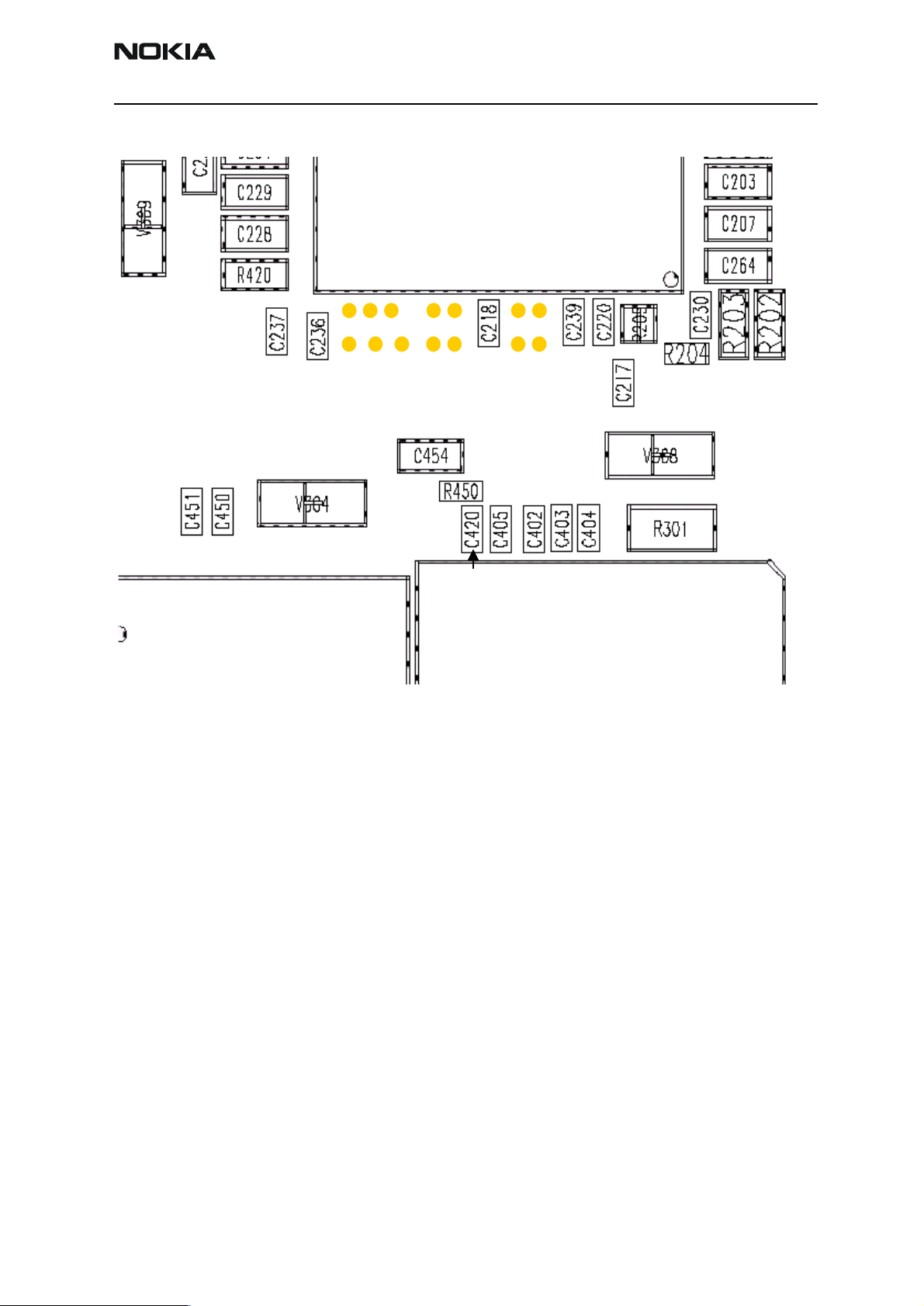
Measurement points
Figure 1: UEM regulator's filter capacitors
COR
FLAS
FLAS
UEM
VSIM
Page 6 ãNokia Corporation Issue 1 11/02
Page 7
RH-13
UEMINT
PURX
DbusCLK
FbusRX
Dbu
sENX
MbusRX
MbusTX
UEM
FLASH
UPP
CCS Technical Documentation Troubleshooting
Figure 2: BB testpoints
RFCLK:
Init clk
19.22MHz
GSM 13MHz
Issue 1 11/02 ãNokia Corporation Page 7
Page 8
RH-13
Troubleshooting CCS Technical Documentation
Baseband Troubleshooting
Note: ESN and IMEI has to re-written to phone If UEM is replaced. This can be
done only in Central Service.
The Baseband Troubleshooting instructions consists of the following topics:
•Power up
• Flash programming
•Audio
•Earpiece
•Microphone
• Charging
• Accessory detection
• Data cable
•Sleep clock
• User interface
•Display
•Lights
•Buzzer
•Vibra
•Keyboard
•Infra red
• Power up faults
Power up sequence
UEM acts as a HW master during start up
• Vbatt limits: 2.1V for internal state machine, 3V triggering whole startup
• Regulator sequencing
Page 8 ãNokia Corporation Issue 1 11/02
Page 9

RH-13
CCS Technical Documentation Troubleshooting
•Hw "core" regulators "on": Vio, Vcore, VR3, Vflash1
•These regulators are supplying the processors, memory, chip interfaces and
clock source in RF
• Reset releasing delay
•Supply voltages stabilize to their UEM hw default values
•RFCLK grows to full swing
•Core is ready to run but waiting for PURX release
• Reset releasing
•UPP releases the SLEEPX up to "non sleep" -state to prevent the UEM switching
the regulators "OFF"
MCU starts running the Bootstrap Code
•written in stone/ UPP internal ROM
•the program checks if there exists any reason for FDL mode (Flash Down Load)
•If there exists executable code in FLASH and there exists no reason for FDL, the
MCU starts running the MCU program from FLASH.
MCU runs the FLASH MCU code
•the phone initialization, user interfaces, internal blocks etc
•Core regulator voltage setting for required DSP speed
•Initializes the DSP and concerning hw
•Releases DSP reset -> DSP starts running
Note: In the figure below RF_Clk frequency appears to be lower than 19.2MHz
because of too low oscilloscope sampling frequency (2kS/s).
Issue 1 11/02 ãNokia Corporation Page 9
Page 10

RH-13
Troubleshooting CCS Technical Documentation
Figure 3: Power up sequence
1 Power key pressed
• After 20ms UEM enters RESET MODE if VBAT>Vmstr+
2 2) VFLASH1, Vana, Vcore, Vio and VR3 goes high.
• VCTCXO enabled by VR3 -> RFClk 19.2 MHz running.
3 Purx released
• Purx released by UEM, UEMINT goes high for 100 ms and about
500ms RFCLK will change 13MHz (GSM mode), SleepX goes high and
UEM startsfeeding SleepClk (32 KHz) to UPP. NOTE! Sleepclock starts
running in crystal circuitry (B200) immediately when battery voltage is
supplied.
4 Software running
• Default value for Vcore is 1.5 volts and if software is running Vcore will
rise to 1.8 volts.
• Cbus (1.00MHz/GSM and 1.08MHz/TDMA) clock starts running.
Page 10 ãNokia Corporation Issue 1 11/02
Page 11

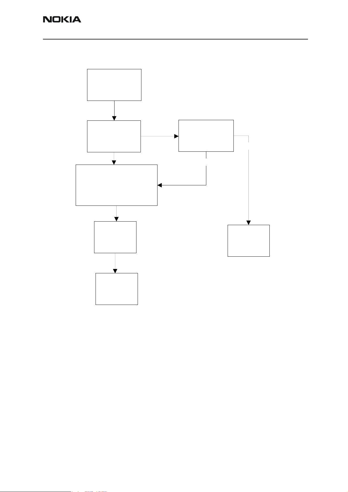
RH-13
CCS Technical Documentation Troubleshooting
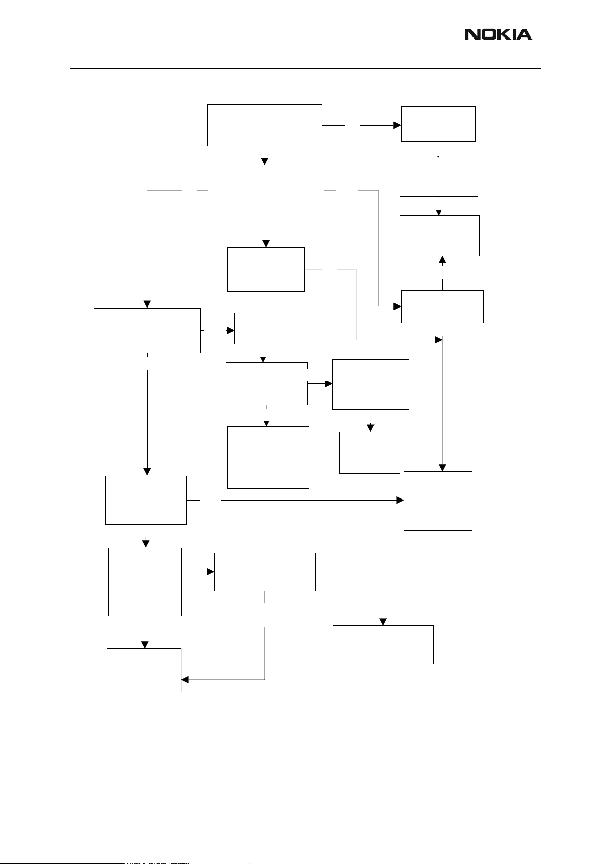
Phone does not start up normally or does not stay on
Note! In case of power up faults, it's not possible to force phone on by disabling watchdog. Instead, measurements should be done immediately when power key pressed or
when battery voltage connected to phone (local/test mode).
The easist way to check if software is running when phone takes abnormal amount of
current is to measure cbusclk and Vcore.
Dbus clock (programmable 9.72MHz TDMA, 13MHz GSM) is not automatically visible on
test and local mode.
Issue 1 11/02 ãNokia Corporation Page 11
Page 12
RH-13
Troubleshooting CCS Technical Documentation
Figure 4: Fault tree, phone does not power up
OK
Check 13MHz /GSM
or 19.44/TDMA
RF-clock from C420
OK
Tryto start phone to
testor local mode
FAIL
Measure
Vflash1,Vana,Vio,Vcore
,VR3 when pwrkey
pressed
VR3
missing
Check G801
(missing,
misaligned)
FAIL
Check
C420
OK
Check 19.2MHz
from G801
OK
FAIL
OK
FAIL
R816,C867,C8
66, R817, C868
OK
Check
Check the
powerkey
OK
Check R202,
R203, R205,
C217, C220
OK
Check
X101,C108,
C109,Z101
FAIL
Measure VBAT
from C262
OK
OK
troubleshooting
Check that purx
goes up to 1.8V
OK
Measure J406.
1.08
MHz/TDMA
and
1.00MHz/GSM
OK
Change UPP
(D400)
FAIL
FAIL
Re-flash phone
Programmng ok,
but phone doesn't
start
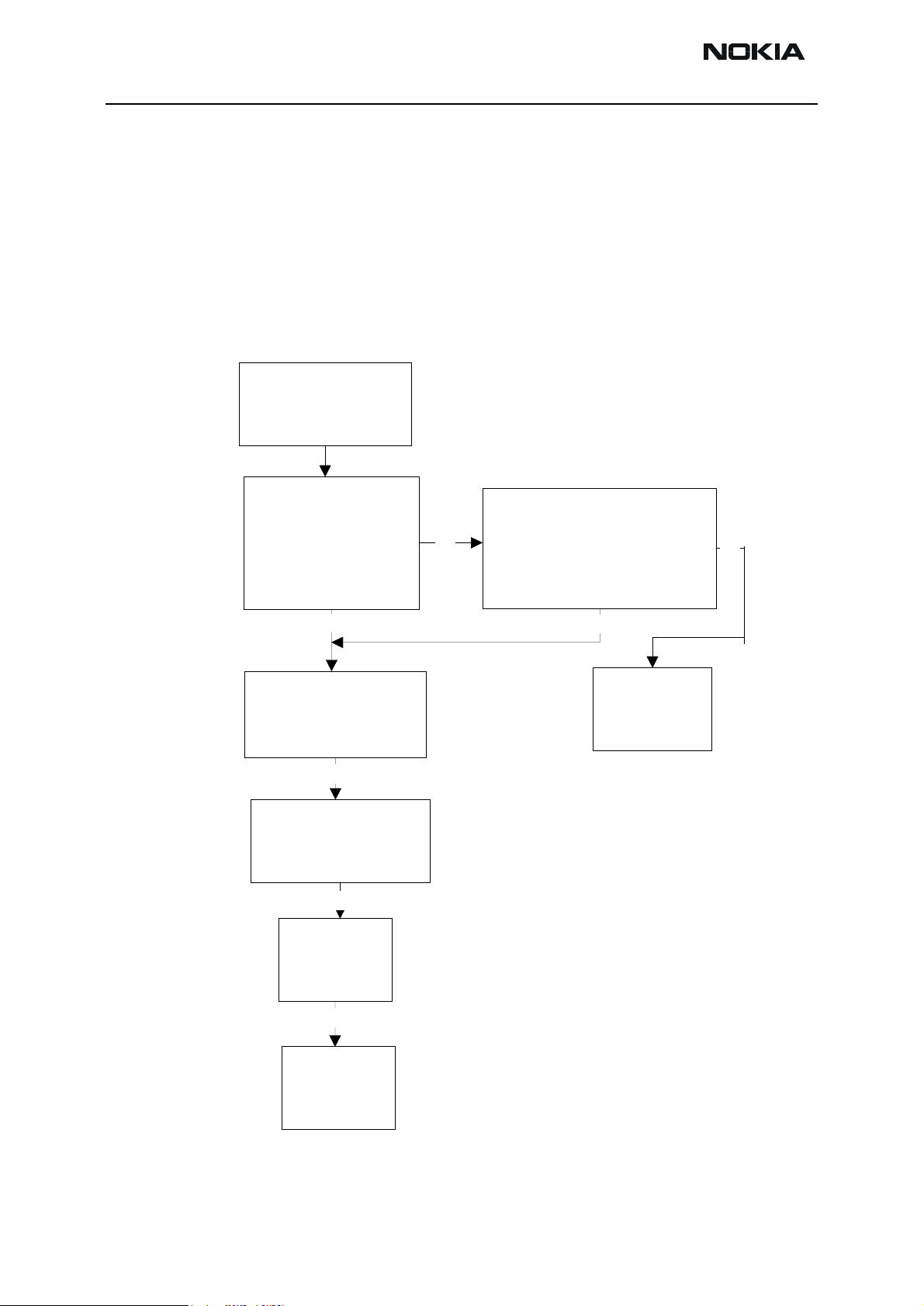
Flash Programming does not work
See RF
Change
G801
Change the
UEM (D200)
Programming
fails
Go to flash failure
chart
Flash programming procedure
• Phone communicates with prommer via production test pattern, using signals:
Page 12 ãNokia Corporation Issue 1 11/02
Page 13

RH-13
CCS Technical Documentation Troubleshooting
•FBUSTX(serial data to phone),
•FBUSRX(serial data from phone),
•MBUS(serial clock for FBUSRX)
•VPP(External flashing voltage for speed up flashing)
• Also BSI line is used when initializing flashing (battery connector)
• When phone is powered (VBAT>3V ) MBUS and FBUSTX lines are pulled up internally by phone.
• Prommer sends command to UEM, using FBUSRX, to enter Flash-mode. During
the sending of this command prommer keeps BSI line high and MBUS is used as a
serial clock.
• When Flash-mode command is acknowledged UEM enters Flash-mode and
releases reset (PURX) to MCU.
• After reset is released UPP checks if there is a request for Bootstrap code (that
resides in UPP ROM).
• Request for Bootstrap is MBUS pulled down by Prommer. (If bootstrap is not
requested, bootstrap code jumps to FLASH SW.)
• If Bootstrap code is requested UPP enters Flash-mode and sets FbusTX to '0' as
acknowledgement to prommer. This is an indication that UPP can run, at least,
the fixed Bootstrap code – although not able to run FLASH code. UPP then sends
an UPP-ID to prommer via FBUSTX line.
• After prommer has received UPP-ID it sends corresponding Secondary Boot Code
to phone via FBUSRX. Secondary Boot Code, when run in UPP, requests UPP to
send information to prommer about flash type and other HW related parameters
about the device to be flashed.
• Prommer then sends the Algorithm Code
and this algorithm, when run in UPP, takes over handling the MCUSW transfer to
Flash.
corresponding to the HW parameters
• 12 volts can be supplied to Vpp (by prommer) to speedup flashing.
• FLASH Program includes a package of MCU and DSP software and all default
parameters for the phone. The tuning values will be added/rewritten during
Flash/Alignment phase.
Issue 1 11/02 ãNokia Corporation Page 13
Page 14
RH-13
Troubleshooting CCS Technical Documentation
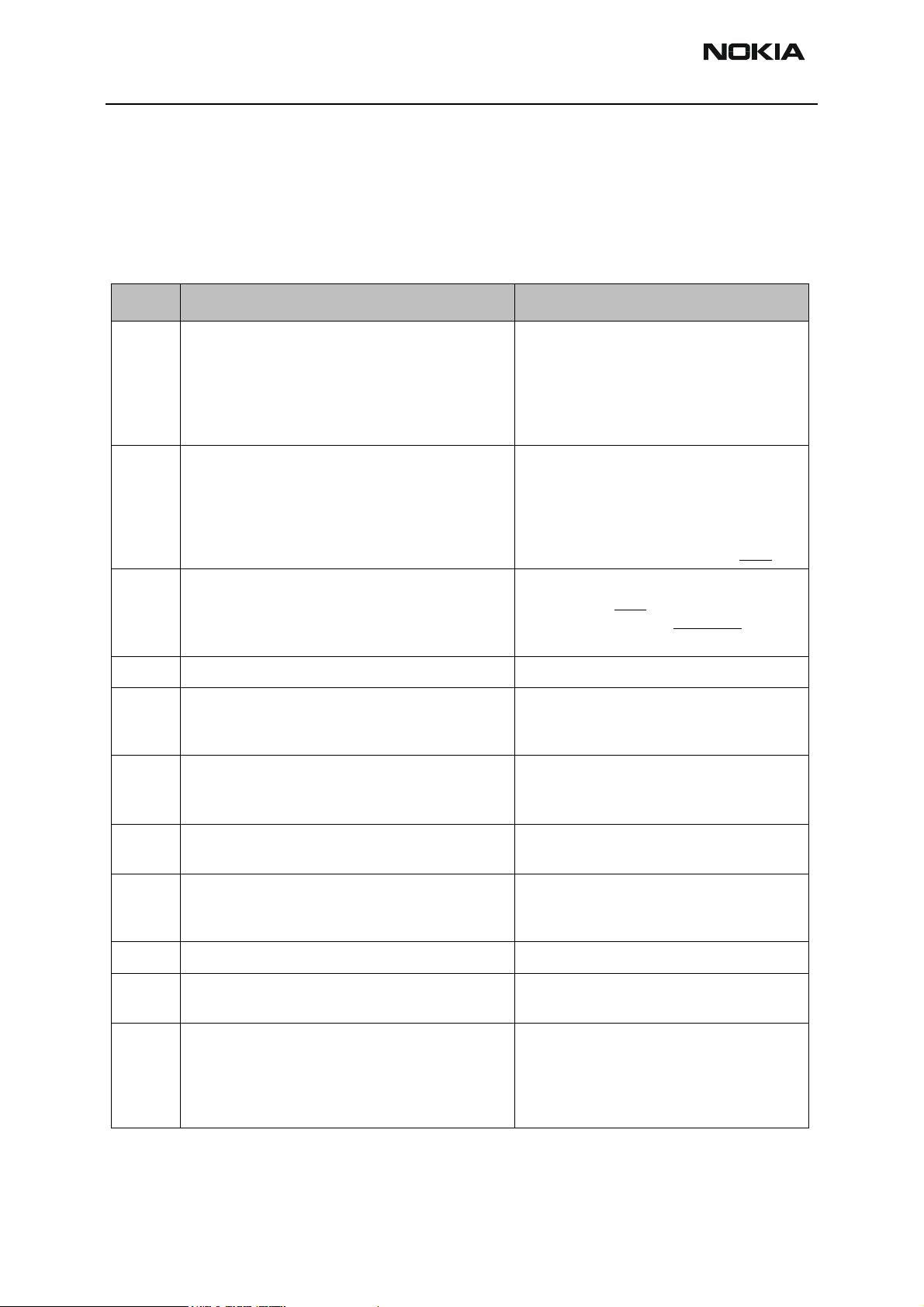
Flash programming error codes
Error codes can be seen from "FPS-8 Flash" in Phoenix.
Underlined note means that item under consideration is being used first time in flashing
sequence.
Table 2: Flash programming error codes
Error Description Not working properly
C101 "The Phone does not set FbusTx line high after the
startup."
C102 "The Phone does not set FbusTx line low after the
line has been high. The Prommer generates this
error also when the Phone is not connected to the
Prommer."
C103 "Boot serial line fail." Mbus from Prommer->UEM-
C104 "MCU ID message sending failed in the Phone." FbusTx from UPP->UEM->Prommer
C105 "The Phone has not received Secondary boot codes
length bytes correctly."
C106 "The Phone has not received Secondary code bytes
correctly."
Vbatt
Vflash1
Vcore
VIO
BSI and FbusRX from prommer to UEM.
FbusTx from UPP->UEM->Prommer(SA0)
PURX(also to Safari)
VR3
Rfclock(VCTCXO->Safari->UPP)
Mbus from Prommer->UEM>UPP(MbusRx)(SA1)
FbusTx from UPP->UEM->Prommer(SA1)
>UPP(MbusRx)(SA0)
FbusRx from Prommer->UEM->UPP
FbusTx from UPP->UEM->Prommer
Mbus from Prommer->UEM->UPP(MbusRx)
FbusRx from Prommer->UEM->UPP
FbusTx from UPP->UEM->Prommer
Mbus from Prommer->UEM->UPP(MbusRx)
FbusRx from Prommer->UEM->UPP
FbusTx from UPP->UEM->Prommer
C107 "The Phone MCU can not start Secondary code cor-
rectly."
A204 " The flash manufacturer and device IDs in the
existing Algorithm files do not match with the IDs
received from the target phone."
A387 "The MCU ID in the MCUSW UPP
C601 "The prommer has detected that Vpp voltage level
has dropped below the limit"
C383
C583
C683
"The Prommer has not received Phone acknowledge
to the message."
(C383-during algorithm download to target phone)
(C583-during erasing)
(C683-during programming)
UPP
Flash
Signals between UPP-Flash
Vpp from prommer - >Flash
Flash
UPP
Signals between UPP-Flash
Page 14 ãNokia Corporation Issue 1 11/02
Page 15
RH-13
CCS Technical Documentation Troubleshooting
C384
C584
C684
C585
C685
C586
C686
"The Phone has generated NAK signal during data
block transfer."
(C384-during algorithm download to target phone)
(C584-during erasing)
(C684-during programming)
Data block handling timeout"
(C585-during erasing)
(C685-during programming)
"The status response from the Phone informs about
fail."
(C586-during erasing)
(C686-during programming)
Flash
UPP
Signals between UPP-Flash
Flash
UPP
Signals between UPP-Flash
Flash
Issue 1 11/02 ãNokia Corporation Page 15
Page 16
RH-13
Troubleshooting CCS Technical Documentation
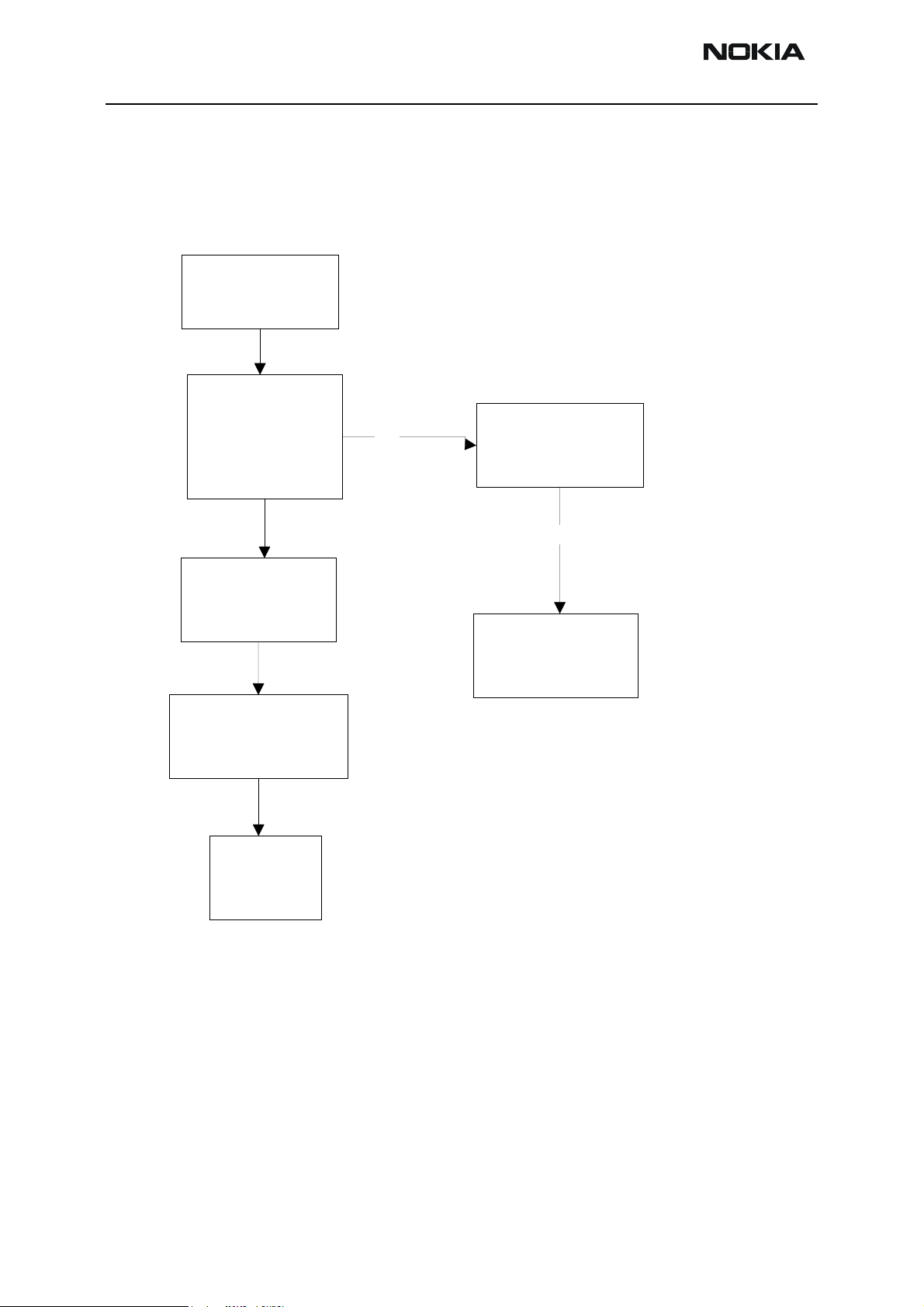
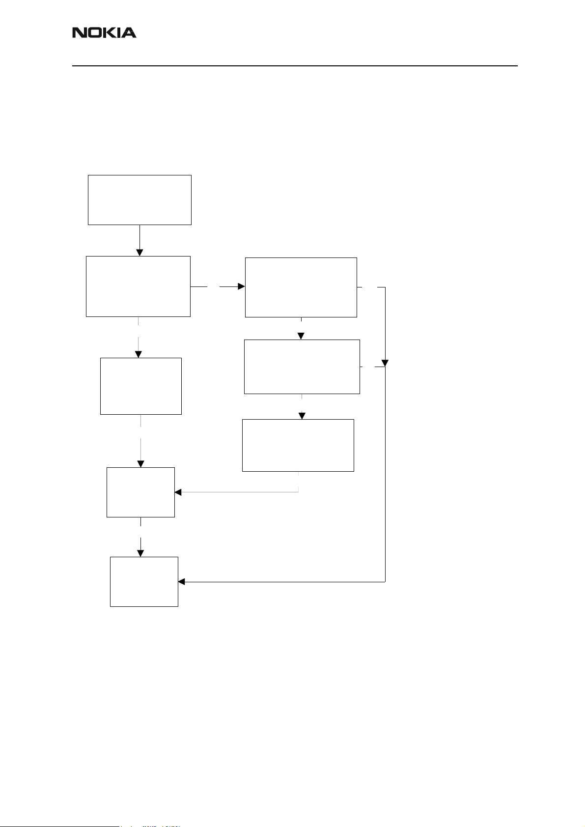
Charging
Note: Charging voltage and current can be checked by connecting phone to service
software and reading ad- converter values of vchar and ichar.
Figure 5: Fault tree, charging
Phone doesn't start
charging
Connectchargerand
check VCHARIN,
check CHRG_CTRL
if used ACP-9,
LCH-8, LCH-9,
DCH-12, HFU-2
Fail
F100,L100,V100,C105
Check
, R107,C107
OK
Check ICHAR
FAIL
Check
R202,R203,R205,C217,
C220,C201,C202 and
R200
OK
Changethe
UEM
OK
Check bottom
connector
-VIN
- CHRG_CTRL
Audio failures
In case of audio failures there are three possibilities to check audio lines.
1 Make a phone call against tester and check audios.
2 In case of earpiece/XMIC fail: Feed 1Khz signal to XMIC line and measure signal
from earpiece line. Audio test box JBA-8 is needed. Audio loop (Audio test/Ext In
Hp Out) must be switched on by Phoenix service software. This loop will connect
audios only through UEM. In this case UPP is not used.
Page 16 ãNokia Corporation Issue 1 11/02
Page 17

RH-13
CCS Technical Documentation Troubleshooting
3 In case of internal microphone/XEAR fail: Feed tone to microphone and measure
signal from XEAR line. Audio test box JBA-8 is needed. Audio loop (Audio test/Hp
In Ext Out) must be switched on by Phoenix service software. This loop will connect audios only through UEM. In this case UPP is not used.
4 Run audio- loop selftest with Phoenix (BB Self tests/ST_EAR_DATA_LOOP_TEST).
This loop will test the eardata/micdata lines between UPP and UEM.
Issue 1 11/02 ãNokia Corporation Page 17
Page 18

RH-13
Troubleshooting CCS Technical Documentation
Earpiece or external microphone line does not work
Figure 6: Fault tree, earpiece fail
Earpiecedoesn't
work
Run audio-loop
selftest with
phoenix
OK
Check R157,L152,
L158,C150,C164,
C153, C165,R152,
C156,C155,R164,
R161,R153,R150,
C159,C167,V153
OK
Check
earpiece
OK
ChangeUEM
Fail
Feed 1KHz to Xmic
by JBA-8 and
measurefrom
earpiece
Fail
OK
Change UPP
Page 18 ãNokia Corporation Issue 1 11/02
Page 19
RH-13
CCS Technical Documentation Troubleshooting
Microphone or XEAR does not work
Figure 7: Fault tree, microphone fail
Microphone doesn't
work
Run audio-loop
selftest with
phoenix
Ok
Check
C151,C152,C157,L151,C162,
C168,C169,R156,R162,R166,
R159,C154,C158,C161,C166,
R163,L159,V152
Ok
Check
microphone
Ok
ChangeUEM
Fail
Feed 1KHz to Mic
and measurefrom
Xear by JBA-8
Fail
Ok
ChangeUPP
Issue 1 11/02 ãNokia Corporation Page 19
Page 20
RH-13
k
Troubleshooting CCS Technical Documentation
Accessory detection
• - Start phone to normal mode when checking accessory detection.
• - Ad- converter value of headint and hookint - lines can be checked with Phoenix
ADC-reading.
• - When headset HDC-9 connected and headset push button is held down, headint- value should be between 10 and 50 and hookint- value between 0-30.
Figure 8: Fault tree, accessory detection
Accessory detection
doesn'tworknormally
Check HeadInt and
HookInt ad-value with
Phoenix
(No accessory
connected)
- HeadInt and HooInt
~1000
Fail
Check headint-line
L152,C150,R152,C153,
R154,
C160,R153,R150,C159
Ok
Check hookint-line
L159,R163,C158,R155,
R151,C161,V152
Ok
Ok
ConnectHDC-9 and keep the
HDC-9 switch close while
reading headint and hookint
ad-value.
Both values should go close to
zero (~0...50)
Fail
Calibrate ADC
and check
accessory
detection again
O
Check bottom
connector
Ok
Change UEM
Page 20 ãNokia Corporation Issue 1 11/02
Page 21
RH-13
CCS Technical Documentation Troubleshooting
Power supply for data cable
DLR-3 needs power supply for data transfering. SGND will supply 2.8V to DLR-3.
- Start phone to normal mode when checking DLR-3 detection
Figure 9: Fault tree, data cable.
DLR-3 data cable
doesn't work
Connect DLR-3,check
DLR-3 detection
Fail
Check the
componentsof
XMIC, HEADINT
and MICB2 lines
Ok
Check bottom
connector
Ok
Ok
Check VFlash2
(~2.8V)
OK
Check SGND voltage from
bottomconnector
(2.40-2.90V)
Fail
Check V151,V152,R161,
C164,L158
Ok
Fail
Ok
Change UEM
Sleep Clock
Missing/non-functional sleep clock causes
• Entering sleep mode fails (higher current consumption -> shorter standby time)
• Baseband self tests cannot be run
Issue 1 11/02 ãNokia Corporation Page 21
Page 22

RH-13
Troubleshooting CCS Technical Documentation
• Phone clock (on display) does not function properly
Figure 10: Fault tree, sleep clock
Sleep mode
not working
Measure sleep clock
from J404
Ok
Change UPP
(D400)
Fail
Measure sleep clock
from B200
Ok
ChangeUEM
(D200)
Fail
Check C203
&C204
Ok
Change B200
Page 22 ãNokia Corporation Issue 1 11/02
Page 23
RH-13
CCS Technical Documentation Troubleshooting
Display/Keyboard lights do not work
Figure 11: Fault tree, Display/Keyboard lights
Display/Keyboard
lights are not working
Check R300 (Display)and
R301 (Keyboard)
OK
Check LEDs
V300...V303,V310-V311
(Display)and V304...V309
(Keyboard)
OK
Use Display Test in
Phoenix to set lights
ON/OFF
FAIL
FAIL
FAIL
Replace
resistor(s)
Replace
LED(s)
Replace UEM
Issue 1 11/02 ãNokia Corporation Page 23
Page 24

RH-13
Troubleshooting CCS Technical Documentation
Display does not work
Figure 12: Fault tree, display
Displaydoes not work
Check that phon e
powers up no rmally
(current consumption,
power up sequence)
OK
Check display visually
(possible crack s on
COG driver o r glass,
capacitors loose or
broken
OK
Check PW B and
elastomer
connector
FAIL
FAIL
FAIL
Proceed to phone
doesn't power up
troubleshootin g
Replace
displaymodule
Clean PWB and
replace
elastomer if
needed
In any phase of display
troubleshooting use Display Test in
Phoenix to produce test patterns on
display.
Also check w ith a known good
display module to see if it w orks.
OK
Run LCD test in
Phoenix
(BB Se lf Te s ts/
ST_LCD_TEST)
OK
Use Display Test
in Phoenix to
check if display
works
FAIL
Replace
displaymodule
FAIL
Check
capacitors
C302...C304
OK
Replace
elastomer
FAIL
FAIL
Replace
capacitors(s)
Replace
display module
Buzzer does not work
Check spring connectors and C306.
Page 24 ãNokia Corporation Issue 1 11/02
Page 25

RH-13
CCS Technical Documentation Troubleshooting
No sound: Try using known good buzzer instead. If still no sound ->change UEM(D200)
Weak sound: Use Audio test in Phoenix to set buzzer parameters(frequency, strength). If
it doesn't effect to the sound level ->change buzzer.
Vibra does not work
Check spring connectors and C307.
No vibration: Try using known good vibra instead. If still no vibration -> change
UEM(D200)
Weak vibration: Use Vibra test in Phoenix to set vibra parameters(frequency, duty cycle).
If it doesn't effect to the magnitude of vibration ->change vibra.
Keyboard does not work
Check that there is no dirt between the dome sheet and the PWB, also check that Z300 is
properly soldered and the corner mark is located in the right place. If the keyboard still
doesn't operate normally -> try to use Keyboard test in Phoenix to see if the pressed key
is identified. If not ->change UPP(D400), then if this does not help, also change the
Z300.
SIM does not work
Check SIM reader's spring connectors, C390 (VSIM 3.0V) and R388. If SIM still does not
work then probably the UEM or the UPP is broken -> change first one component and
check the phone.
Issue 1 11/02 ãNokia Corporation Page 25
Page 26

RH-13
Troubleshooting CCS Technical Documentation
Infrared does not work
Figure 13: Fault tree, infra red
Infra Red no t working
Measure Vflash1 from IR
module VCC(pin6), should
be 2.78V
OK
Check R350, R351, C351
and V350
OK
Use
ST_IR_LOOP_TEST(in
BB Self Te sts) in Phoenix
FAIL
FAIL
FAIL
OK
Change
UEM(D200)
Replace faulty
component(s)
Use
ST_IR_IF_TEST(in
BB Sel f Tests) in
Phoenix
FAIL
OK
Measure Tx Data from
IR modu le (pin3 )
2.78V, 9.6/115.2kbps
UPP or UEM is faulty
Measure Rx Data from
OK
Change UEM
IR module(pin4)
OK
Phone OK
FAIL
Change IR module
Page 26 ãNokia Corporation Issue 1 11/02
Page 27

RH-13
CCS Technical Documentation Troubleshooting
RF troubleshooting
Repairing instructions for RF Unit
Introduction
Measurements should be done using spectrum analyzer and high-frequency probe (Local
and reference frequencies and RF-power levels in intermediate stages of chain). Oscilloscope is used to measure DC-voltages and low frequency signals. Multimeter is also useful measurement equipment in faultfinding. Also cellular tester is needed in order to
perform tests mentioned in this document.
External RF connector is implemented to design improving reliability of the measurement
results and should be in use when it is reasonable.
RF-section is mainly build around of SAFARI GTE IC (N801). The RF block has separate
external filters, UHF and VHF synthesizer, Power Amplifier, front-end and up converter
circuit for both frequency band.
To simplifying troubleshooting, this RF troubleshooting document is divides into three
bigger sections: Receiver-, Transmitter and Synthesizer parts. The tolerance is specified
for critical signals/voltages.
Before changing single ASICs or components, please check the following things:
1 The soldering and alignment marks of the ASICs
2 Supply voltages and control signals are OK
The PA-module is static discharge sensitive! ESD protection must be used when dealing with PA-IC (ground straps and ESD soldering irons). The PA is also moisture sensitive
components and it is important to follow additional information about handling the
component. So wear EDS protected clothes and shoes whenever handling the radio module unit! Also wrist-grounding strap should be used.
The shield lid must be always replaced with new one after it is opened. Plate bands under
shield lid could be cut but always bend plate ends downwards after repairing. Plate ends
should NOT touch shield lid after lid is installed. Note also that there are no short circuits
caused by plate ends on PWB.
Issue 1 11/02 ãNokia Corporation Page 27
Page 28

RH-13
Troubleshooting CCS Technical Documentation
Abbreviations in fault finding chart
AF: Audio Frequency
BB Base band
BPF Band pass filter
f: Frequency of signal (measured with spectrum analyzer)
HB High band
LB Low band
LO Local Oscillator
P: Power of signal in decibels (dB) (measured with spectrum analyzer)
PA Power Amplifier
PWB Printed Wiring Board
PWRDET Power detector module
PLL Phase Locked Loop
RF Radio Frequency
RX Receiver
T: Time between pulses
TX Transmitter
U/C Up converter (mixer and driver in same package)
UHF Ultra High Frequency
V: Voltage of signal (measured with oscilloscope)
VCO Voltage controlled oscillator
VHF Very High Frequency
Page 28 ãNokia Corporation Issue 1 11/02
Page 29

RH-13
CCS Technical Documentation Troubleshooting
Receiver
General instructions for RX troubleshooting
Receiver troubleshooting is divided into three sections:
- General checking
- Local oscillator checking
- RX Chain checking
Faultfinding charts are represented for each band and more detailed troubleshooting
instructions are included. Please note that before changing ASICs or filters, all solderings
and missing components must be checked visually. After any possible component
changes phone must be re-tuned using Phoenix.
Equipment needed for receiver troubleshooting:
- Signal generator up to 2 GHz
- Oscilloscope with 10x passive probe
- Spectrum analyzer and active probe without attenuation block
- PC with Phoenix SW
Issue 1 11/02 ãNokia Corporation Page 29
Page 30

RH-13
Duplex filter
Duplex filter
Diplex filter
LNA
1900
LNA
850
Band
filter
Band
filter
1
st
mixer
1
st
mixer
GS
M
TDMA
AGC
AGC
2
nd
mixer
2
nd
mixer
BB filter
BB filter
AGC
AGC
Q
I
UHFLOVHF
LO
2063.4 ... 2124 MHz
AGC 1...31 dB, 5 steps
AGC
AGC
-
6...30 dB, 5 steps, GSM
AGC 25/20 dB 1 step
Troubleshooting CCS Technical Documentation
Path of the received signal
Block level description of the receiver:
Figure 14: Receiver block diagram
1930 ... 1990 MHz 869 ... 894 MHz
850 / 1900
133.2 MHz
BW
200 kHz
1900 MHz
850 MHz
134.04 MHz
ch filter
Buffer Buffer
BW
30 kHz
SAFARI GTE
1002.4...1028.01MHz
(VCO / 2)
ch filter
133.2 MHz (VCO / 2)
134.04 MHz (VCO / 2)
Page 30 ãNokia Corporation Issue 1 11/02
-6...36 dB, 7 steps, TDMA
QI
Page 31

RH-13
CCS Technical Documentation Troubleshooting
AMPS
Fault finding chart
A pply signal to ext.
antenna connector
f= 881.4 M H z (ch 380)
mod.= 1004 Hz
dev.= 8 kHz
level= -116 dBm
Connect audio box
from the bottom
connector to audio
analyzer
SINAD < 12 dB
A pply signal to ext.
antenna connector
f= 881.409 MHz
(ch 380)
unmodulated
level= -50 dBm
Check signal level
at diplexer Z 908
input
SINAD > 12 dB
Not OK
AMPS RX is OK
Replace external
antenna connector
X900
OK
Check signal level
at duplex filter
Z906 input
Not OK
Replace diplexer
Z908
OK
Check signal level
at L N A _a input
coil pad (L 802)
Not OK
If coil L 802 is ok
replace duplex
filter Z906
OK
Issue 1 11/02 ãNokia Corporation Page 31
Page 32

RH-13
Troubleshooting CCS Technical Documentation
Step 1. General checking
Check signal level
at RX band filter
Z801 input
OK
Check signal level
at mix1_A input
OK
Check signal level
at IF filter Z 803
input (134.04
MHz)
OK
Check signal level at
IF filter Z 803 output
(134.04 MH z)
Not OK
Not OK
Not OK
Not OK
Measure V R 4 from
Check components
Replace IF filter
these ok => replace
L812 and
L 811pads
Not OK
L 812,
L811 etc.
Z803
Check V R 4 supply
and components if
Safari N801
Replace RX band
filter Z 801
OK
Start synthesizer
troubleshooting
OK
Replace Safari N801
OK
Check signal level at
R X I/Q J808, J809,
J818, J819
OK
Check UEM and
start baseband
troubleshooting
Not OK
Start synthesizer
troubleshooting
OK
Replace Safari N801
Page 32 ãNokia Corporation Issue 1 11/02
Page 33

RH-13
CCS Technical Documentation Troubleshooting
Audio test
Please use Phoenix RF-control to set phone to the correct operation mode.
Figure 15: RF Test
Enable audio using Phoenix software (maintenance -> testing -> audio test mode -> set
audio test mode). See picture below.
Figure 16: Audio Test
Issue 1 11/02 ãNokia Corporation Page 33
Page 34

RH-13
Troubleshooting CCS Technical Documentation
Step 2. Local oscillator checking
Carrying out this step VCO signal of 1st and 2nd mixers can be checked. 2nd mixer RX
VHF VCO frequency is constant 268.08 MHz but for the 1st mixer UHF VCO frequency
depends on the channel. The UHF VCO frequencies for the 1st mixer are:
Channel 991: 2006.16 MHz
Channel 380: 2030.88 MHz
Channel 799: 2056.02 MHz
1 Set signal generator frequency to 881.4091125 and level to -80 dBm.
2 Set phone to TDMA mode and select RF Test UI in Phoenix (Maintenance => Test-
ing => RF Test).
Figure 17: RF Test.
3 Make sure that signal generator allows phone TX power going to its output. Use
low power level, for example 10. Set channel to 380 and select "Write Init".
4 Set spectrum analyzer settings as following:
• Center frequency: 268.08 MHz, Span: 200 kHz
• RBW: 3 kHz, reference level: 0 dBm
5 Connect spectrum analyzer probe on the inductor L818 and record RX VHF VCO
signal level and frequency. Signal level should be around -25 dBm and frequency
268.08 MHz.
6 Set spectrum analyzer settings as following:
• Center frequency: 2030.88 MHz, Span: 200 kHz
Page 34 ãNokia Corporation Issue 1 11/02
Page 35

RH-13
CCS Technical Documentation Troubleshooting
• RBW: 3 kHz, reference level: 10 dBm
7 Connect spectrum analyzer probe to the UHF VCO output and record signal level
and frequency. Signal level should be around -5 dBm and frequency 2030.88
MHz.
Output
G802
8 Repeat measurement for channels 991 and 799.
Step 3. RX chain checking
1 Set signal generator frequency to 881.4091125 and level to -50 dBm.
2 Set phone to TDMA mode and select RF Test UI in Phoenix (Maintenance => Test-
ing => RF Test).
3 Make sure that signal generator allows phone TX power going to its output. Use
low power level, for example 10. Set channel to 380 and press "Write Init".
4 Connect oscilloscope probe to one of the RX I/Q test points on PWB (all four
testpoints J808, J809, J818 and J819 are located behind display)
5 Check that there is a clean signal in each test points.
6 Decrease signal level slowly down to -115 dBm and make sure that AGC keeps
signal in visible (This can be noticed by looking at the RX I/Q voltage during signal level change).
7 Measure and record the frequency and peak-to-peak voltage of RX I/Q signal
from each test points. Voltage should be around 100 mVp-p and frequency 6.5
kHz +/- 3 kHz.
Issue 1 11/02 ãNokia Corporation Page 35
Page 36

RH-13
K
K
p
K
Troubleshooting CCS Technical Documentation
TDMA800
Since there is same physical signal path for both analog (AMPS) and digital modes
(TDMA/GSM) in lower band there is no need for additional troubleshooting in digital
modes. If digital mode in lower band is not working properly start analog mode troubleshooting.
GSM850
Figure 18: Fault finding chart.
Apply signal to ext.
antenna connector
f= 881.46771 MHz
(ch 189)
unmodulate
level= -80 dBm
Check signal level
at RX I/Q J808,
J809, J818, J819
Not OK
Check signal level
at diplexer Z908
input
Check signal level
at duplex filter
Z906 input
Check signal level
At LNA_a input
coil
ad (L802)
O
O
OK
Not OK
Not OK
Not OK
GSM850 RX is
OK
Replace external
antenna connector
X900
Replace diplexer
Z908
Replace duplex
filter Z906
O
Page 36 ãNokia Corporation Issue 1 11/02
Page 37

RH-13
K
K
K
K
K
K
K
CCS Technical Documentation Troubleshooting
Step 1. General checking
Figure 19: General checking.
Check signal level
at RX band filter
Z801 input
O
Check signal level
at mix1_A input
O
Check signal level
at IF filter Z804
input (133.2 MHz)
O
Not OK
Not OK
Not OK
Measure VR4 from L815
and L814 pads
Not OK
Check components
L815,
L814 etc.
Check V R 4 supply
and components if
these ok => replace
Replace RX band
Safari N801
filter Z801
O
Start synthesizer
troubleshooting
OK
Replace Safari N801
Check signal level
at IF filter Z804
output (133.2
MHz)
Check signal level
at RX I/Q J808,
J809, J818, J819
Check UEM and
start baseband
troubleshooting
Not OK
O
Not OK
O
Replace IF filter
Z804
Start synthesizer
troubleshooting
O
Replace Safari
N801
The fastest way to get overview of RX status is to measure RSSI (Received Signal
Strength Indicator) level. This can be done by using signal generator and Phoenix. Note
that this is useful only if the phone has been calibrated when it was OK and the malfunction have occured after tunings.
1 Set signal generator frequency to 881.46771 MHz and level to -80 dBm.
2 Select RSSI measurement UI in Phoenix (Maintenance => GSM RSSI Meas).
3 Set Band to GSM850 and Rx/Tx channel to 189
Issue 1 11/02 ãNokia Corporation Page 37
Page 38

RH-13
Troubleshooting CCS Technical Documentation
Figure 20: GSM RSSI Measurement.
If the cable losses are calibrated correctly the RSSI reading should give reasonable result
(-80 dBm +/- 2 dB). Please note that RSSI result is valid only if there has not been RX
calibration attempts for the faulty phone. If the RSSI level is several dB's lower go to
Step 2 (Local oscillator checking).
Step 2. Local oscillator checking
Carrying out this step VCO signal of 1st and 2nd mixers can be checked. 2nd mixer RX
VHF VCO frequency is constant 266.4 MHz but for the 1st mixer UHF VCO frequency
depends on the channel. The UHF VCO frequencies for the 1st mixer are:
Channel 128: 2004.8 MHz
Channel 189: 2029.2 MHz
Channel 251: 2054.0 MHz
1 Set phone receiver to continuous mode using Phoenix.
2 Set spectrum analyzer settings as following:
• Center frequency: 266.4 MHz, Span: 200 kHz
• RBW: 3 kHz, reference level: 0 dBm
Page 38 ãNokia Corporation Issue 1 11/02
Page 39

RH-13
CCS Technical Documentation Troubleshooting
3 Connect spectrum analyzer probe on the inductor L818 and record RX VHF VCO
signal level and frequency. Signal should look like in the picture below:
Figure 21: RX VHF VCO signal level and frequency.
4 Set spectrum analyzer settings as following:
• Center frequency: 266.4 MHz, Span: 200 kHz
• RBW: 3 kHz, reference level: 0 dBm
5 Connect spectrum analyzer probe on the inductor L818 and record RX VHF VCO
signal level and frequency.
6 Set Rx/Tx channel to 189 using Phoenix.
7 Set spectrum analyzer settings as following:
• Center frequency: 2029.2 MHz, Span: 200 kHz
• RBW: 3 kHz, reference level: 10 dBm
Issue 1 11/02 ãNokia Corporation Page 39
Page 40

RH-13
Troubleshooting CCS Technical Documentation
8 Connect spectrum analyzer probe to the UHF VCO output and record signal level
and frequency. Signal level should be around -5 dBm and frequency 2029.2 MHz.
Figure 22: UHF VCO.
Output
G802
9 Repeat measurement for channels 128 and 251.
Step 3. RX chain checking
1 Set signal generator frequency to 881.46771 MHz and level to -80 dBm.
2 Set phone receiver to continuous mode with full gain using Phoenix.
Figure 23: RF controls
3 Connect oscilloscope probe to one of the RX I/Q test points on PWB (all four
testpoints J808, J809, J818 and J819 are located behind display)
Page 40 ãNokia Corporation Issue 1 11/02
Page 41

RH-13
CCS Technical Documentation Troubleshooting
4 Measure frequency and peak-to-peak voltage of RX I/Q signal from each test
points. Signal should look like in the picture below:
Figure 24: RX I/Q signal.
• If only one or two testpoints shows correct signal and rest of the testpoints are
either deaf or signal is very small, the fault is probably due to Safari ASIC.
• If the signal amplitude is correct but its frequency is something else than 67.71
kHz +/- 3 kHz, you may try to change AFC value (-1024...1023) and see does it
have effect to the frequency. Frequency should be tuned to target value with the
AFC value of +/- 100.
• If the signal amplitude and frequency in all testpoints is correct and signal
amplitude changes when the LNA, MIX2 and BB gains are changed, RX chain is
OK.
• If the signal amplitude in all testpoints is too low (< 1 Vp-p), you have to continue with RX front-end measurements.
1 Set signal generator frequency to 881.46771 MHz and level to -60 dBm.
2 Set spectrum analyzer settings as following:
• Center frequency: 133.2 MHz, Span: 200 kHz
• RBW: 3 kHz, reference level: -20 dBm
Issue 1 11/02 ãNokia Corporation Page 41
Page 42

RH-13
Troubleshooting CCS Technical Documentation
3 Set phone receiver to continuous mode with full gain using Phoenix (see figure
23, RF controls, in step 3).
4 Connect spectrum analyzer probe to the output of GSM IF filter (at the one end
of R804) and record the level.
5 Connect spectrum analyzer probe to the input of GSM IF filter (at the one end of
R803) and record the level.
• If the IF signal levels are according to the picture below and local oscillators are
OK (see step 2 Local oscillator checking) but RX I/Q signal is not correct (see step
3 to check RX I/Q signal) the problem is probably due to malfunction of either
2nd mixer or AGC blocks inside Safari.
• If the IF signal level is correct at the filter input but not at the output side the filter shall be replaced with new one.
• If the IF signal level is not correct at the filter input side and the local oscillators
are functioning properly, inductors L814 and L815 should be checked, as well. If
they are OK and there is a signal at the input of the 1st mixer, the problem is
probably due to a faulty 1st mixer inside Safari.
Figure 25: IF signal level
LNA gain step function can be checked by measuring signal level at L806 and turning ON
and OFF the LNA using Phoenix. The gain should change by 20...30 dB.
TDMA1900
Only path from external RF connector to IF needs to be checked if AMPS/TDMA800/
GSM850 RX chain is OK. After down conversion (from RF to 134.04 MHz IF) both lower
and upper band use same signal path.
Page 42 ãNokia Corporation Issue 1 11/02
Page 43

RH-13
T
X
CCS Technical Documentation Troubleshooting
Figure 26: Fault finding chart.
Apply signal to ext.
antenna connector
f= 1960.029 MHz ch
1000)
unmodulate
level= -50 dBm
Check signal level
at RX I/Q J808,
J809, J818, J819
Not OK
Check signal level
at diplexer Z908
input
OK
Check signal level
at duplex filter
Z962 input
OK
Check signal level
atLNA V804 input
OK
Check signal level
at RX band filter
Z 802 input
OK
Not OK
Not OK
Not OK
Not OK
DMA1900 RX is
OK
Replace external
antenna connector
900
Replace diplexer
Z908
Replace duplex
filter Z962
Check components
around lna and
measure supply
voltages
OK
Check signal level
at mix1_B input
OK
C ontinue
troubleshooting as
in
AMPS/TDMA800
Not OK
Replace RX band
filter Z802
Step 1. Local oscillator checking
Carrying out this step VCO signal of 1st and 2nd mixers can be checked. 2nd mixer RX
VHF VCO frequency is constant 268.08 MHz but for the 1st mixer UHF VCO frequency
depends on the channel. The UHF VCO frequencies for the 1st mixer are:
Issue 1 11/02 ãNokia Corporation Page 43
Page 44

RH-13
Troubleshooting CCS Technical Documentation
Channel 2: 2064.12 MHz
Channel 1000: 2094.06 MHz
Channel 1998: 2124.00 MHz
1 Set signal generator frequency to 1960.0230375 MHz and level to -80 dBm.
2 Set phone to TDMA mode and select RF Test UI in Phoenix (Maintenance => Test-
ing => RF Test).
Figure 27: RF Test.
3 Set channel to 1000 and press "Write Init".
4 Set spectrum analyzer settings as following:
• Center frequency: 268.08 MHz, Span: 200 kHz
• RBW: 3 kHz, reference level: 0 dBm
5 Connect spectrum analyzer probe on the inductor L818 and record RX VHF VCO
signal level and frequency. Signal level should be around -25 dBm and frequency
268.08 MHz.
6 Set spectrum analyzer settings as following:
• Center frequency: 2094.06 MHz, Span: 200 kHz
• RBW: 3 kHz, reference level: 10 dBm
7 Connect spectrum analyzer probe to the UHF VCO output and record signal level
and frequency. Signal level should be around -5 dBm and frequency 2094.06
Page 44 ãNokia Corporation Issue 1 11/02
Page 45

RH-13
Output
CCS Technical Documentation Troubleshooting
MHz.
G802
8 Repeat measurement for channels 2 and 1998.
Issue 1 11/02 ãNokia Corporation Page 45
Page 46

RH-13
Troubleshooting CCS Technical Documentation
GSM1900
Figure 28: Fault finding chart
A pply signal to ex t.
antenna connector
f= 1960.06771 MHz
(ch 661)
unmodulated
level= -80 dBm
Check signal level
at RX I/Q J808,
J809, J818, J819
Not OK
Check signal level
at diplexer Z908
input
OK
Check signal level
at duplex filter
Z962 input
OK
Check signal level
atL N A V 804 input
OK
Not OK
Not OK
Not OK
G SM1900 RX is
OK
Replace external
antenna connector
X900
Replace diplexer
Z908
Replace duplex
filter Z962
OK
Chart is continued on the next page.
Page 46 ãNokia Corporation Issue 1 11/02
Page 47

RH-13
CCS Technical Documentation Troubleshooting
Check signal level
at RX band filter
Z802 input
OK
Check signal level
at mix1_B input
OK
Check signal level
at IF filter Z804
input (133.2 MHz)
OK
Not OK
Not OK
Not OK
Measure V R4 from L 815
and L 814 pads
Not OK
C heck components
L 815,
L 814 etc.
Check components
around lna and
measure supply
voltages
Replace RX band
filter Z802
OK
Start synthesizer
troubleshooting
OK
Replace Safari N801
Check signal level
at IF filter Z804
output (133.2
MHz)
OK
Check signal level
at R X I/Q J808,
J809, J818, J819
OK
Check UEM and
start baseband
troubleshooting
Not OK
Not OK
Replace IF filter
Z 804
Start synthesizer
troubleshooting
OK
Replace Safari
N801
Issue 1 11/02 ãNokia Corporation Page 47
Page 48

RH-13
Troubleshooting CCS Technical Documentation
Step 1. General checking
The fastest way to get overview of RX status is to measure RSSI (Received Signal
Strength Indicator) level. This can be done by using signal generator and Phoenix. Note
that this is useful only if the phone has been calibrated when it was OK and the malfunction have occured after tunings.
1 Set signal generator frequency to 1960.06771 MHz and level to -80 dBm.
2 Select RSSI measurement UI in Phoenix (Maintenance => GSM RSSI Meas).
3 Set Band to GSM1900 and Rx/Tx channel to 661
Figure 29: GSM RSSI Measurement.
If the cable losses are calibrated correctly the RSSI reading should give reasonable result
(-80 dBm +/- 2 dB). Please note that RSSI result is valid only if there has not been RX
calibration attempts for the faulty phone. If the RSSI level is several dB's lower go to
Step 2 (Local oscillator checking).
Step 2. Local oscillator checking
Carrying out this step VCO signal of 1st and 2nd mixers can be checked. 2nd mixer RX
VHF VCO frequency is constant 266.4 MHz but for the 1st mixer UHF VCO frequency
depends on the channel. The UHF VCO frequencies for the 1st mixer are:
Channel 512: 2063.4 MHz
Channel 661: 2093.2 MHz
Channel 810: 2123.0 MHz
Page 48 ãNokia Corporation Issue 1 11/02
Page 49

RH-13
CCS Technical Documentation Troubleshooting
1 Set phone receiver to continuous mode using Phoenix.
2 Set spectrum analyzer settings as following:
Figure 30: RF controls.
• Center frequency: 266.4 MHz, Span: 200 kHz
• RBW: 3 kHz, reference level: 0 dBm
3 Connect spectrum analyzer probe on the inductor L818 and record RX VHF VCO
signal level and frequency. The result should be like in the picture below:
Figure 31: RX VHF VCO signal level and frequency
4 Set Rx/Tx channel to 661 using Phoenix.
5 Set spectrum analyzer settings as following:
• Center frequency: 2093.2 MHz, Span: 200 kHz
• RBW: 3 kHz, reference level: 10 dBm
Issue 1 11/02 ãNokia Corporation Page 49
Page 50

RH-13
Troubleshooting CCS Technical Documentation
6 Connect spectrum analyzer probe to the UHF VCO output and record signal level
and frequency. Signal level should be around -5 dBm and frequency 2093.2 MHz.
Output
G802
The result should be like in the picture below:
Figure 32: UHF VCO signal level and frequency
7 Repeat measurement for channels 512 and 810.
Page 50 ãNokia Corporation Issue 1 11/02
Page 51

RH-13
CCS Technical Documentation Troubleshooting
Step 3. RX chain checking
1 Set signal generator frequency to 1960.06771 MHz and level to -80 dBm.
2 Set phone receiver to continuous mode with full gain using Phoenix.
Figure 33: RF controls.
3 Connect oscilloscope probe to one of the RX I/Q test points on PWB (all four
testpoints J808, J809, J818 and J819 are located behind display)
4 Measure frequency and peak-to-peak voltage of RX I/Q signal from each test
points. Signal should look like in the picture below:
Figure 34: RX I/Q signal.
• If only one or two testpoints shows correct signal and rest of the testpoints are
either deaf or signal is very small, the fault is probably due to Safari ASIC.
• If the signal amplitude is correct but its frequency is something else than 67.71
Issue 1 11/02 ãNokia Corporation Page 51
Page 52

RH-13
Troubleshooting CCS Technical Documentation
kHz +/- 3 kHz, you may try to change AFC value (-1024...1023) and see does it
have effect to the frequency. Frequency should be tuned to target value with the
AFC value of +/- 100.
• If the signal amplitude and frequency in all testpoints is correct and signal
amplitude changes when the LNA, MIX2 and BB gains are changed, RX chain is
OK.
• If the signal amplitude in all testpoints is too low (< 1 Vp-p), you have to continue with RX front-end measurements.
1 Set signal generator frequency to 1960.06771 MHz and level to -60 dBm.
2 2) Set spectrum analyzer settings as following:
• Center frequency: 133.2 MHz, Span: 200 kHz
• RBW: 3 kHz, reference level: -20 dBm
3 Set phone receiver to continuous mode with full gain using Phoenix (see figure
33, RF controls, in step 3).
4 Connect spectrum analyzer probe to the output of GSM IF filter (at the one end
of R804) and record the level.
5 Connect spectrum analyzer probe to the input of GSM IF filter (at the one end of
R803) and record the level.
• If the IF signal levels are according to the picture below and local oscillators are
OK (see step 2 Local oscillator checking) but RX I/Q signal is not correct (see step
3 to check RX I/Q signal) the problem is probably due too malfunction of either
2nd mixer or AGC blocks inside Safari.
• If the IF signal level is correct at the filter input but not at the output side the filter shall be replaced with new one.
• If the IF signal level is not correct at the filter input side and the local oscillators
are functioning properly, inductors L814 and L815 should be checked, as well. If
they are OK and there is a signal at the input of 1st mixer, the problem is probably due to faulty 1st mixer inside Safari.
Page 52 ãNokia Corporation Issue 1 11/02
Page 53

RH-13
CCS Technical Documentation Troubleshooting
Figure 35: IF signal level.
LNA gain step function can be checked by measuring signal level at L803 and turning ON
and OFF the LNA using Phoenix. The gain should change by 20...30 dB.
Transmitter
General instructions for TX troubleshooting
Always use an RF-cable connected from an external RF-connector to analyzer via (rfpower) attenuator. This is important to protect analyzer against excessive RF power and
not allow leakage of undesired RF power into cellular frequencies.
After any component change tune the phone with Phoenix auto tune SW.
AMPS/TDMA
Start Phoenix-software and select TX mode under testing (AMPS, DAMPS or TDMA1900).
It is useful to select mid channel (383 for AMPS/DAMPS or 1000 for TDMA1900) and
power level 2. Select random data for digital mode of operation.
GSM850
Start Phoenix-software and select GSM RF Control, Band GSM850, Active unit TX, PL7,
Ch189 and TX data type random.
GSM1900
Start Phoenix-software and select GSM RF Control, Band GSM1900, Active unit TX, PL0,
Ch661 and TX data type random.
Path of the transmitted signal
AMPS/DAMPS, GSM850
UEM TX I/Q DA-converters -> I/Q modulator and Digital gain step amplifier (SAFARI) ->
Dual TX IF-BPF -> Up converter (mixer -> C904 -> driver) -> BPF -> PA -> Power detector -> Duplex-filter -> Diplexer -> EXT RF-connector -> Antenna
Issue 1 11/02 ãNokia Corporation Page 53
Page 54

RH-13
Troubleshooting CCS Technical Documentation
TDMA1900, GSM1900
UEM TX I/Q DA-converters -> I/Q modulator and Digital gain step amplifier (SAFARI) ->
Dual TX IF-BPF -> Up converter (Mixer -> BPF -> Driver) -> BPF -> PA -> Power detector
-> Duplex-filter -> Diplexer -> EXT RF-connector -> Antenna
The power detection and power control circuit belongs under power control part of this
guide.
Figure 36: TX signal path.
1900
UHF-PLL 2G (÷2)
(2063.4-2124 MHz, HB)
D
I
P
800
D
E
T
1900MHz
800MHz
1900MHz
800MHz
(1003.08-1028.01 MHz,LB)
213.2 MHz
214.08 MHz
178.2 MHz
179.04 MHz
DIV
2
VHF-PLL
356.4 MHz
358.08 MHz
426.4 MHz
428.16 MHz
VHF
VCO
I
Q
Page 54 ãNokia Corporation Issue 1 11/02
Page 55

RH-13
CCS Technical Documentation Troubleshooting
Fault finding charts for transmitter
AMPS
Start Phoenix-software and set phone to the Analog mode. Set channel 383 and Power
level 2. Connect RF-cable to Ext RF connector and connect cable to Spectrum analyzer
input and measure RF level. Please notice insertion loss of the cable and attenuations.
Figure 37: RF Test.
Figure 38: RF controls.
Issue 1 11/02 ãNokia Corporation Page 55
Page 56

RH-13
Troubleshooting CCS Technical Documentation
Figure 39: Fault finding chart
AMPS,PL2, CH383
Visual check of TX
block
- PA and up converter
-TX SAW
- Duplex filter
- Passive components
OK
*)Check LO-signal
(1015.53MHz)
@L979&L980
and TX VHF (358.08
MHz)@N811
OK
Check supply voltages:
VR2,VBATTRF,
VR5, IPA1,BANDSEL,
TX_ENABLE
TX_GAIN_CONTROL
OK
Check T Xi/q signals
Test points J810...J811
OK
**)Check TX IF power
(179.04 MHz) @
C931&C932
Input: -17 dBm
+3 /-6 dB
NOK
NOK
NOK
NOK
Start synth
troubleshooting
Check UEM and UPP
(Baseband)
Check UEM
(Baseband)
Change SAFARI
N801
OK
***)Check TX RF
(836.49 MHz) output
power @ U/C output
RF: -5 dBm +/- 6dB
OK
NOK
1) Check C904
2) Change
U/C N902
Page 56 ãNokia Corporation Issue 1 11/02
Page 57

RH-13
CCS Technical Documentation Troubleshooting
Check TX SAW
input an d output power
IL: 3 dB
OK
****)Is Itot 680 ... 1000
mA?
Check PA output power
and gain.
Output power: ~2 8 dBm
Gain: ~30 dB
OK
Check PW RDET N900
insertion loss
IL<0.3 dB
OK
NOK
Change TX SAW filter
Z905
NOK
Change PA N901
NOK
Change PW RDET
N900
Check duplexer Z906,
diplexer Z908 and RF
connector X90 0
Dupl IL: ~2.2 dB
Dipl IL: ~0.35 dB
RF conn: ~0.1 dB
OK
Start Power control
troubleshooting
NOK
Change Z906 or Z908
or RF connector
*) GSM850 LO-signal freq. 1014.6 MHz and TX VHF-signal freq. 356.4 MHz
**) GSM850 TX IF freq. 178.2 MHz and level –17 dBm
***) GSM850 TX RF freq. 836.4 MHz and level 0 dBm
****) GSM850 Itot 170 – 300 mA
Issue 1 11/02 ãNokia Corporation Page 57
Page 58

RH-13
Troubleshooting CCS Technical Documentation
TDMA800, GSM850
The transmitter chain is exactly same as the AMPS mode, except for the IPA current, and
thus it is important that the AMPS circuitry has no faults.
TDMA1900, GSM1900
TDMA1900 and GSM1900 mode and DAMPS mode have a common RF modulator and
thus it is important that DAMPS mode have no faults.
Figure 40: TDMA1900.
Figure 41: GSM1900.
Page 58 ãNokia Corporation Issue 1 11/02
Page 59

RH-13
CCS Technical Documentation Troubleshooting
Figure 42: Fault finding chart
TDMA1900, PL2, CH1000
GSM1900, PL0, CH6 61
NOK
Is TDMA800 mode
OK?
OK
Start AMPS
troubleshooting
Check LO-signal
(TDMA 2094.06 GSM
2093.2MHz)@L979&L98
0andTXVHF
(TDMA 428.16
GSM 4 26.4 MHz)@N811
OK
Check supply voltages:
VR2,VBATTRF,
VR6, IPA2,BANDSEL,
TX_ENABLE
TX_GAIN_CONT RO L
OK
Check TX IF input
power (T DMA 214.08
GSM 2 13.2 MHz) @
C931&C932
IF:-12 dBm +6/-6dB
OK
Check TX RF (TDMA
1879.98 GSM 1880
MHz) U/C output power
@ Z961 input
TDMA +4 dBm +/- 6dB
GSM +8 dBm +/- 6dB
NOK
NOK
NOK
NOK
Start synth
troubleshooting
Check UEM and UPP
(Baseband)
Change SAFARI N801
or Z901
1) Che ck Z96 0 input
and output power
IL: -3 dB
2) C han ge U/C N902
OK
Check Z961 input and
output power
IL: -3dB
OK
NOK
Change Z961
Issue 1 11/02 ãNokia Corporation Page 59
Page 60

RH-13
Troubleshooting CCS Technical Documentation
Is Itot TDMA 350...500
GSM200 ... 300 mA?
CheckPA output power
and gain. Gain: ~30 dB
Pout:TDMA ~29 dBm
GSM~32 dBm
OK
CheckPWRDET N900
insertion loss
IL< 0.3 dB
OK
Checkduplexer Z962 ,
diplexer Z908 and RF
connector X900
insertion loss
Dupl IL ~2.2 dB
Dipl ~0.35 dB
RF conn ~0.1 dB
NOK
Change PA N901
NOK
Change PWRDET
N900
NOK
Change Z962 or Z908
or RF connector
OK
Start Powercontrol
troubleshooting
Page 60 ãNokia Corporation Issue 1 11/02
Page 61

RH-13
t
CCS Technical Documentation Troubleshooting
Power control loop
Basically, the power detection is done with Power detector module and power control is
done inside SAFARI. Power detection is similar for both bands, except both bands have
own coupler.
Figure 43: Power detection.
Note !
See TXPWRDET vs. Outpu
power curve
Is TXPWRDET vs.
output power OK?
See chart below.
Y
Is DAC value vs.
TXPWRDET (mV)
OK?
N
N
Check VR2 and
PATEMP .
Check C921, C922
and PWRDET
module.
Check UEM
(BaseBand)
The detected voltages are illustrated in the following table and diagram.
AMPS AND TDMA
TXPWRDET values can be checked with Phoenix autotuning.
Table 3: TYPICAL DETECTED VOLTAGES AT POWER LEVELS PL2…PL10
800A 800D 1900
D
Pout TXPWRDET Pout TXPWRDET Pout TXPWRDET
PL dBm dac mV dBm dac mV dBm dac mV
2 25.7 450 27.3 27.3 503
3 23.3 301 23.3 23.3 304
4 19.3 179 19.3 19.3 182
5 15.3 107 15.3 15.3 105
6 11.1 60 11.1 11.1 57
7 7.0 33 7.0 7.0 30
8 - - - 3.0 18 3.0 15
9 - - - -1.0 8 -1.0 6
10 - - - -5.0 3 -5.0 2
Issue 1 11/02 ãNokia Corporation Page 61
Page 62

RH-13
Troubleshooting CCS Technical Documentation
GSM850/GSM1900
GSM detected voltages and DAC values are also OK if AMPS and TDMA values are OK.
NOTE: DAC VALUES MAY VARY ABOUT +/- 20%NOTE: TXPWRDET is difference between TX
on burst and off burst.
Table 4: Typical detected voltages at power levels PL0...PL19.
Pout TXPWRDET Pout TXPWRDET,
U_value
PL dBm dac mV dBm dac mV
0 - - 29.5
1 - - 28
2 - - 26
3 - - 24
4 - - 22
5 - - 20
6 - - 18
7 29.5 16
8 27 14
9 25 12
10 23 10
11 21 8
12 19 6
13 17 4
14 15 2
15 13 0
16 11 - 17 9 - 18 7 - 19 5 - -
Page 62 ãNokia Corporation Issue 1 11/02
Page 63

RH-13
CCS Technical Documentation Troubleshooting
Synthesizers
There are five oscillators generating the needed frequencies for RF section. 19.2 MHz reference oscillator, 2GHz UHF VCO, TX VHF cascade amplifier VCO both RX VHF VCO and
BB VHF integrated in Safari. RX VHF frequency is 268.08 MHz in TDMA and 266.4 MHz in
GSM and TX VHF has four fixed frequencies, 358.08 MHz TDMA and 356.4 MHz GSM for
lowband and 426.4 MHz in GSM and 428.16 MHz in TDMA upper band. VCO's operating
frequencies are controlled by PLL-circuit of SAFARI. All locals are locked to a stable 19.2
MHz reference oscillator.
The frequency range for 2GHz UHF VCO is: 2004.8 … 2124 MHz. The output frequency
range for the lower band is from 2006.16 to 2056.02 MHz in TDMA and from 2004.8MHz
to 2054 in GSM. In TDMA upper band the output frequency range is from 2064.12 MHz
to 2124 MHz and GSM 2063.40 to 2123 MHz.
BB-PLL frequencies are in TDMA 77.76 MHz and in GSM 78 MHz
It is a practical way to check out synthesizer status by measuring the control voltage of
the VCO from Integrator capacitor. If the voltage is stable and reasonable, local oscillators are running correctly.
19.2 MHz reference oscillator
The 19.2 MHz oscillator frequency (G801) is controlled by UEM. This 19.2 MHz signal is
connected thru SAFARI to PLL-circuits.
All synthesizers use divided VCTCXO signal as a reference signal for Phase locked loop to
provide correct LO-frequency.
BB-PLL provides to the BB needed clock signals.
Issue 1 11/02 ãNokia Corporation Page 63
Page 64

RH-13
Troubleshooting CCS Technical Documentation
Figure 44: Fault finding chart for 19.2 MHz oscillator
2
Change
VCTCXO
OK
2.No
START HERE!
Is VCTCXO
oscillating?
19.2MHz
C867
2.78 V
No
R816
OK
1
OK
1.No
Check voltage
Check resistor
OK!
Page 64 ãNokia Corporation Issue 1 11/02
Page 65

RH-13
CCS Technical Documentation Troubleshooting
RX VHF VCO
The RX VHF VCO signal is used to generate receiver Intermediate frequency. RX VHF VCO
has two fixed frequencies: TDMA 268.08 MHz, GSM 266.4 MHz. Operating frequency is
locked in Phase locked Loop.
RX VHF VCO output signal is fed to SAFARI. Inside the SAFARI signal is divided for Phase
detector and RX parts. Before I/Q-modulator frequency is divided by 2.
Fault finding chart for RX VHF VCO
Note! Measure oscillator frequency over L818 coil. Don’t connect probe to pads!
AMPS/TDMA -> RX VHF frequency 268.08 MHz
GSM -> RX VHF frequency 266.4 MHz
Figure 45: Fault finding chart for RX VHF VCO.
4
3
Check loopifilter
components:
C848, R808, C847,
R807, C846, R820, C870
check also R826
OK
3.No
Change
SAFARI
No
1 START HERE
Is oscillator locked
to TDMA 268.08
or GSM 266.4
OK
MHz
2.No
Check resonator
OK
2
components:
Yes
OK!
V801, C845, C871,
L818 and DC block C821
Issue 1 11/02 ãNokia Corporation Page 65
Page 66

RH-13
RFCLK to BB
*Data are related to vctcxo frequency and mode selections.
Troubleshooting CCS Technical Documentation
BB PLL
The BB PLL generates RF clock to base band. It has two fixed frequencies 77.76 MHz in
TDMA mode and 78 MHz in GSM mode. Next picture shows BB PLL working.
Figure 46: BB PLL.
VCTCXO
Divider
65 or 80
*Data
RF-IC
19.2 MHz
Freq/Phase
comparator
Divider
324 or 325
Divider 4 or 6
Charge Pump
Active
part
BB VCO
Loop Filter
Varactor
Resonator
GSM 13 MHz
TDMA 19.44 MHz
Page 66 ãNokia Corporation Issue 1 11/02
Page 67

RH-13
CCS Technical Documentation Troubleshooting
Fault finding chart for BB PLL
Note! Measure oscillator frequency over L829 coil. Don’t connect probe to pads!
TDMA -> BB PLL frequency 77.76 MHz
GSM -> BB PLL frequency 78 MHz
Figure 47: Fault finding chart for BB PLL.
4
Change
SAFARI
3
Check loopfilter
components:
C878, R834, C881,
R835, C882
OK
3.No
No
1 START HERE
Is o scillator locked
to TDMA 77.76 or
GSM 78 MHz
OK
2.No
Check r esonator
OK
2
components:
V805, C855,
L829 and C893
Yes
OK!
Issue 1 11/02 ãNokia Corporation Page 67
Page 68

RH-13
Troubleshooting CCS Technical Documentation
TX VHF VCO
The TX VHF VCO signal is used to generate transmitter Intermediate frequency. TX VHF
VCO has three fixed frequencies 358.08 MHz for lower band and TDMA 428.16 MHz and
GSM 426.4 MHz for upper band. Operating frequency is locked in Phase locked Loop and
frequency is divided by two before modulator.
Fault finding chart for TX VHF VCO
AMPS, CH383 -> TX VHF frequency 358.08 MHz
TDMA1900, CH1000 -> TX VHF frequency 428.16 MHz
GSM850, CH189 -> TX VHF frequency 356.4 MHz
GSM1900, CH661 -> TX VHF frequency 426.4 MHz
Figure 48: Fault finding chart for TX VHF VCO.
4
Check components:
C853, C852, C851,
R810, R809, R821 and
C841, C873, L828
3
Check resonator
components:
V802, C850, L820,
C874, C865
4.No
OK
3.No
Change
cascade amplifier
OK
Is oscillator locked
5.No
1 START HERE
to 356.4, 358.08,
426.4
or 428.16 MHz
2.No OK
Check operating
voltage:
4.75 V
at R833
5
N811
2
OK
6.No
Yes
No
OK
OK
6
Change
SAFARI
OK!
Check:
L819, R833
Page 68 ãNokia Corporation Issue 1 11/02
Page 69

RH-13
CCS Technical Documentation Troubleshooting
UHF SYNTHESIZER
The UHF synthesizer consists of a external 2GHz UHF VCO, loop filter and integrated PLL
in Safari RF-IC. Safari GTE IC contains stages like counters, prescaler, divider by two,
phase and frequency comparator and a charge pump circuit which allows two operational modes analog and digital. The UHF VCO Oscillation frequency is from 2004.8 MHz
to 2124 MHz
In upper band (TDMA1900 &GSM1900) 2 GHz synthesizer frequency is fed straight to
mixers. In lower band case (AMPS, TDMA800 and GSM850) 2 GHZ UHF VCO frequency
signal is first divided by 2 inside SAFARI and then that divided signal is fed to mixers. The
output frequency of the VCO depends on the DC-control voltage which is controlled by
PLL-circuit inside SAFARI.
Figure 49: Fault finding chart for UHF SYNTHESIZER.
Change
VCO G802
2. No
OK
Checkloopfilter
components and
balun T 8 01,
C863,C862,C861,
C860,R806,
R815,R814,R813
OK
3.
No
START HERE!
Is frequency locked?
2004.8 - 2124
MHz
1.
OK
No
Check VCO
operatig
voltage:
2.78 V
Yes
No
OK
4. No
Is EVM OK?
OK
No
1
Check
loopfilter
components
Check resistor
R811
Change
SAFARIN801
No
YES
low
band
Low band:
Is divided
signal OK?
OK!
Yes
No
Issue 1 11/02 ãNokia Corporation Page 69
Page 70

RH-13
Troubleshooting CCS Technical Documentation
Description of RH-13 RF auto-tune tunings
TDMA RF tunings
Figure 50: Auto tune TDMA
TDMA RX tunings
AFC-Tuning
Purpose of the tuning is to correct phone frequency error
If AFC-tuning fails it might be fue to:
- Problems with lower band signal path, synthesizer etc.
- If AFC DAC tuning value or step size is too low or high it might be due to faulty VCTCXO
component.
- (UEM)
- (UPP)
RX LP and AMP2 filter tunings
- Tuning results are only visible after an unsuccessful auto-tune procedure
Page 70 ãNokia Corporation Issue 1 11/02
Page 71

RH-13
CCS Technical Documentation Troubleshooting
- This tuning has to be done simultaneously with AFC-tuning
If LP and AMP2 filter tunings fail it may be due to:
- Problems with lower band signal path (synthesizer etc.)
- VCTCXO component can be broken
- Safari can be broken or solder joints
UB RX AGC tuning
- UB TDMA minimum gain (around 0 dB), measured when lna is switched off
- UB LNA gain step, measured when lna is switched on. Result is gain difference between
lna on and off (around 20 dB)
- If UB TDMA minimum gain is lower than -2 further analysis is needed. Result 32752
means that the signal doesn't go through RX chain at all or it has a lot of attenuation.
If it fails there can be following problems:
- Rx chain is totally deaf or some gain is missing, start receiver troubleshooting
LB RX AGC tuning
- LB TDMA minimum gain (around 2 dB), measured when lna is switched off
- LB LNA gain step, measured when lna is switched on. Result is gain difference between
lna on and off (around 20 dB)
- If LB TDMA minimum gain is lower than -2 dB, further analysis is needed. Result
32752 means that the signal doesn't go through RX chain at all or it has a lot of attenuation.
If it fails there can be following problems:
- Rx chain is totally deaf or some gain is missing, start receiver troubleshooting
TDMA TX tunings
If some TX tunings fails, start always TX troubleshooting!
TX IQ (TxIq)
- Purpose of the tuning is to tune DC offset and phase offset so low as possible (test limit
–40 dBc)
If tuning fails there can be following problems:
Issue 1 11/02 ãNokia Corporation Page 71
Page 72

RH-13
Troubleshooting CCS Technical Documentation
- UEM or Safari
- Too low output power
TX power levels and crossband (TxPwr)
- Purpose of this tuning is to tune all power levels (PL2 – PL10)
- TX crossband:
- Low band: Purpose is to tune high channel power (ch991) and low channel power
(ch799) equal to mid channel power (ch383).
- Upper band: Purpose is to tune high channel power (ch2) and low channel power
(ch1998) equal to mid channel power (ch1000).
- Crossband tuning is done only with PL2
If tuning fails there can be following problems:
- Broken component: PA, Safari, up converter, some filters
- Missing components
GSM RF tunings
Figure 51: Auto-tune GSM
Page 72 ãNokia Corporation Issue 1 11/02
Page 73

RH-13
CCS Technical Documentation Troubleshooting
GSM RX tunings
LP and AMP2 filters tunings
- This is done using Safari internal loop. No external signal is needed
If it fails there can be following problems:
- Safari problem
GSM AFC tuning
- Purpose of the tuning is to correct phone frequency error
If AFC tuníng fails it might be due to:
- Problems with upper band signal path (synthesizer etc.)
- VCTCXO component can be broken
- (UEM)
- (UPP)
GSM UB LNA GAIN AND RSSI OFFSET
- UB GSM reference gain (around 74 dB), measured when lna is switched off
- UB LNA gain step, measured when lna is switched on. Result is gain difference between
lna on and off (around 21 dB)
If it fails there can be following problems:
- Rx chain is totally deaf or some gain is missing, start receiver troubleshooting
GSM LB LNA GAIN AND RSSI OFFSET
- UB GSM reference gain (around 77 dB), measured when lna is switched off
- UB LNA gain step, measured when lna is switched on. Result is gain difference between
lna on and off (around 20 dB)
If it fails there can be following problems:
- Rx chain is totally deaf or some gain is missing, start receiver troubleshooting
RX temperature calibration
- NTC resistor calibration in ambient temperature
Issue 1 11/02 ãNokia Corporation Page 73
Page 74

RH-13
Troubleshooting CCS Technical Documentation
If NTC temperature fails it might be due to:
- Faulty NTC resistor or pull-up resistor
- faulty UEM
- wrong ambient temperature (phone is too hot or cold)
GSM RX CROSS BAND CALIBRATION
- Purpose of the calibration is to compensate gain ripple due to rx-filters over the band
- This is done in UB and LB
If it fails, response over the band can be very bad and there can be following problems:
- Please check that all components are ok and in place around rx-parts
- Please check that filters are ok
GSM TX tunings
If some TX tuning fails, start always TX troubleshooting!
TX IQ
Purpose of this tuning is to tune DC offset and phase offset so low as possible
- Typical values: Amplitude: -45 to –55 dBc, and Phase: –50 to – 60 dBc
If tuning fails there can be following problems:
- UEM or Safari
- Too low output power
TX Power levels
Purpose of this tuning is to tune all power levels GSM1900 (PL0 – PL15)
and GSM850 (PL7 – PL19)
If tuning fails there can be following problems:
- Broken components: PA, Safari, up converter, some filters
- Missing components
TX crossband
Page 74 ãNokia Corporation Issue 1 11/02
Page 75

RH-13
CCS Technical Documentation Troubleshooting
- GSM1900: Purpose is to tune high channel power (ch512) and low channel power
(ch810) equal to mid channel power (ch661).
- GSM850: Purpose is to tune high channel power (ch128) and low channel power
(ch251) equal to mid channel power (ch189).
Typical values:
- Low Comp Factor UB 0.5, LB 0.5
- High Comp Factor UB 1.0, LB 1.5
PA TROUBLESHOOTING FOR SALIERI
This document has been done to get exact information of defect PA. In case is excessive
current consumption is found during normal trouble shooting, follow this trouble shooting instructions to find out, if the reason is PA. If the failure is due to PA, change the PA
and replace the removed components.
- if the short is on VBATT line, the current consumption goes to maximum provided from
the power supply
- if it is after UEM then the current is high but not maximum.
Compare the current consumption with a working phone.
NOTE! To get specified current readings, turn module jig MJS-17 switches 2 and 3 ON for
local mode.
Issue 1 11/02 ãNokia Corporation Page 75
Page 76

RH-13
N901 1900
N901 850
N901 850
VCC1/VCC2
N901 1900
VCC1/VCC2
No
No
No
No
and check if phone takes
Remove Coil
L903.Current
Remove Coil
L905.Current
Remove Coil
L977.Current
Remove Coil
L978.Current
Troubleshooting CCS Technical Documentation
Figure 52: Fault finding chart
Put the phone PWB in
the module jig MJS-17
toomuchcurrent.Do
not power on.
Yes
PA OK. Check
UEM = BB
troubleshoot.
Yes
Yes
Yes
Report t o additional notes.
VCC3 short.
VCC3 short.
Page 76 ãNokia Corporation Issue 1 11/02
 Loading...