

Page 1

CCS Technical Documentation
RH-13 Series Transceivers
Service Tools
Issue 1 11/02 ãNokia Corporation
Page 2

RH-13
Service Tools CCS Technical Documentation
Contents
Docking Station (JBV-1) and Docking Station Adapter (MJF-1) ................................. 5
Product Code............................................................................................................. 5
View of Docking Station........................................................................................... 5
View of Docking Station Adapter............................................................................. 5
Galvanic Contact (GAC-2) ............................................................................................ 6
Product Code............................................................................................................. 6
View of Galvanic Contact......................................................................................... 6
Flash Adapter (FLA-14)................................................................................................. 7
Product Code............................................................................................................. 7
View of Flash Adapter .............................................................................................. 7
Soldering Jig (MJS-26).................................................................................................. 8
Product Code............................................................................................................. 8
View of Soldering Jig ............................................................................................... 8
Flash Prommer (FPS-8) ................................................................................................. 9
Product Code............................................................................................................. 9
View of Flash Prommer ............................................................................................ 9
Audio Cable (ADS-6) .................................................................................................. 10
Product Code........................................................................................................... 10
View of Audio Cable .............................................................................................. 10
Audio box (JBA-8)....................................................................................................... 11
Product Code........................................................................................................... 11
View of Audio Box ................................................................................................ 11
Mbus/Fbus Cable (XCS-4)........................................................................................... 12
Product Code........................................................................................................... 12
View of Mbus/Fbus Cable....................................................................................... 12
DC Cable (CA-5S)....................................................................................................... 13
Product Code........................................................................................................... 13
View of DC Cable................................................................................................... 13
Power Cable (PCS-1)................................................................................................... 14
Product Code........................................................................................................... 14
View of Power Cable .............................................................................................. 14
RF Cable (XRF-1)........................................................................................................ 15
Product Code........................................................................................................... 15
View of RF Cable.................................................................................................... 15
SW Security Device (PKD-1) ...................................................................................... 16
Product Code........................................................................................................... 16
View of SW Security Device.................................................................................. 16
Power Pack (DDC-10) ................................................................................................. 17
Product Code........................................................................................................... 17
View of Power Pack................................................................................................ 17
Module Jig (MJS-17)................................................................................................... 18
Product Code........................................................................................................... 18
View of Module Jig ................................................................................................ 18
Parallel Flash Prommer (FPS-8C)................................................................................ 19
Product Code........................................................................................................... 19
View of Parallel Flash Prommer............................................................................. 19
POS Flash (FLS-4S)..................................................................................................... 20
Page 2 ãNokia Corporation Issue 1 11/02
Page 3

RH-13
CCS Technical Documentation Service Tools
Product Code........................................................................................................... 20
View of POS Flash Adapter.................................................................................... 20
MBUS Cable (DAU-9P).............................................................................................. 21
Product Code........................................................................................................... 21
View of MBUS Cable DAU-9P.............................................................................. 21
MBUS Cable (DAU-9S).............................................................................................. 22
Product Code........................................................................................................... 22
View of MBUS Cable DAU-9S.............................................................................. 22
Printer Cable (AXP-8) ................................................................................................. 23
Product Code........................................................................................................... 23
View of Printer Cable.............................................................................................. 23
Modular T-adapter ....................................................................................................... 24
Product Code........................................................................................................... 24
View of Modular T-adapter..................................................................................... 24
Gait Test SIM card....................................................................................................... 25
Product Code........................................................................................................... 25
Module Jig MJS-17 0770353....................................................................................... 26
Introduction ................................................................................................................26
List of modules........................................................................................................ 26
Technical Specifications ............................................................................................26
Electrical characteristics......................................................................................... 26
Testing .......................................................................................................................27
Recommended Test Equipment .............................................................................. 27
Test Procedure........................................................................................................ 27
User Instructions ........................................................................................................27
General instruction.................................................................................................. 27
Operation................................................................................................................. 27
Over current and voltage......................................................................................... 27
Assembly ...................................................................................................................28
Construction............................................................................................................ 28
Changeable parts ..................................................................................................... 28
Modifications of MJS-17 for RH-13 .........................................................................29
Change of Alignment pins....................................................................................... 29
SIM Module pwb .................................................................................................... 30
Changing the test pins ................................................................................................30
Pulling the test pins out of pwb............................................................................... 30
Docking Station Adapter MJF-1 0770354................................................................... 31
Introduction ................................................................................................................31
List of Modules ....................................................................................................... 31
Technical Specifications ............................................................................................31
DC Characteristics................................................................................................... 31
D- Connector signals............................................................................................... 31
Mechanical Characteristics ..................................................................................... 33
Environmental Conditions .........................................................................................33
Temperature Conditions.......................................................................................... 33
Testing .......................................................................................................................33
Recommended Test Equipment .............................................................................. 33
Test Procedure......................................................................................................... 33
Issue 1 11/02 ãNokia Corporation Page 3
Page 4

RH-13
Service Tools CCS Technical Documentation
User Instructions ........................................................................................................34
General instruction.................................................................................................. 34
Operation................................................................................................................. 34
Over current and voltage......................................................................................... 34
Assembly ...................................................................................................................34
Construction............................................................................................................ 34
Changing the test pins to MJF-1 ................................................................................34
Flash Adapter FLA-14 0080538 .................................................................................. 36
Introduction ................................................................................................................36
List of Modules ...................................................................................................... 36
Technical Specifications ............................................................................................36
DC Characteristics................................................................................................... 36
Modes of operation.................................................................................................. 36
Mechanical Characteristics .................................................................................... 37
Environmental Conditions .........................................................................................37
Temperature Conditions.......................................................................................... 37
Functional Description ...............................................................................................37
Circuit Description .................................................................................................. 37
Testing .......................................................................................................................37
Recommended Test Equipment .............................................................................. 37
Test Procedure......................................................................................................... 38
User Instructions ........................................................................................................38
General instruction.................................................................................................. 38
Operation................................................................................................................. 38
Assembly ...................................................................................................................38
Construction............................................................................................................ 38
Changing the test pins to FLA-14 ...........................................................................38
Page 4 ãNokia Corporation Issue 1 11/02
Page 5
RH-13
CCS Technical Documentation Service Tools
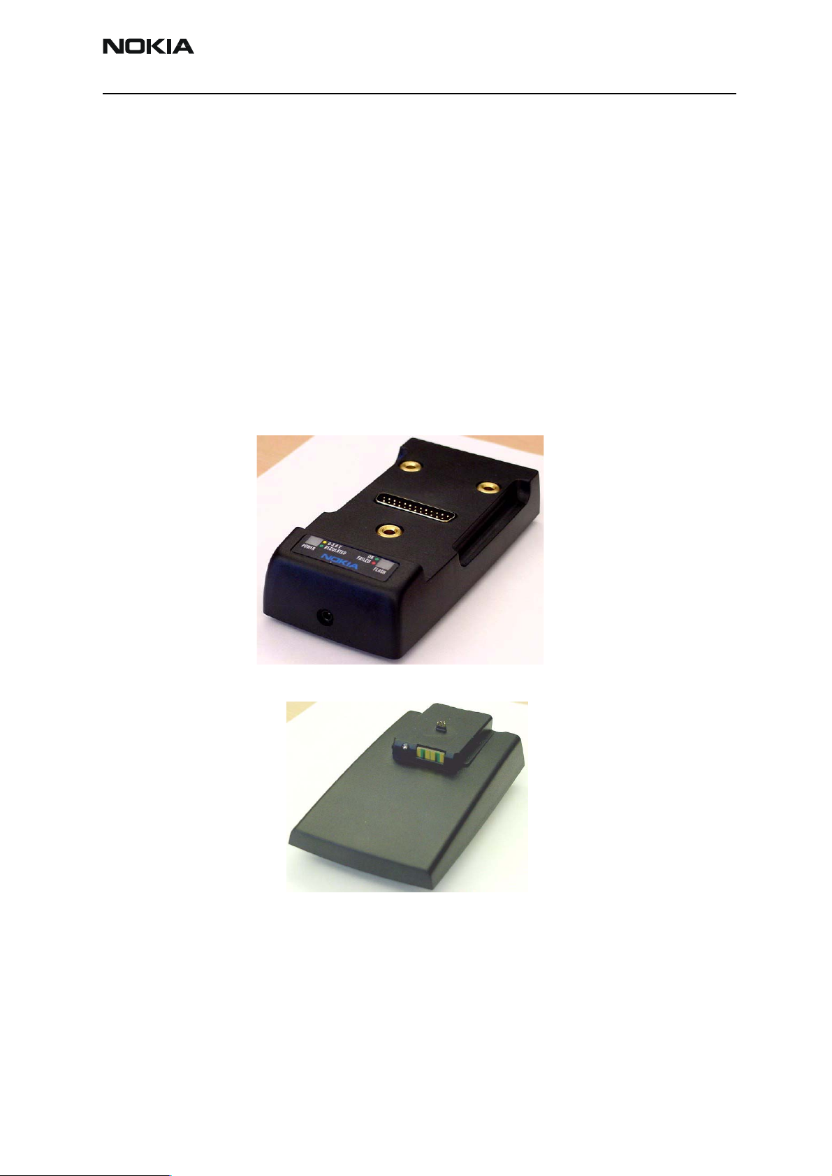
Docking Station (JBV-1) and Docking Station
Adapter (MJF-1)
The Docking Station and the Docking Station Adapter are needed for Mbus, Fbus, RF, and
audio connections.
This setup allows connection between flash prommers. When the audio box is connected,
it has to be connected to the phone’s audio connector. The Docking Station can be powered by FPS-8 or external power supply.
Product Code
Docking Station JBV-1 0770298
Docking Station Adapter MJF-1 0770354
View of Docking Station
View of Docking Station Adapter
Issue 1 11/02 ãNokia Corporation Page 5
Page 6
RH-13
Service Tools CCS Technical Documentation
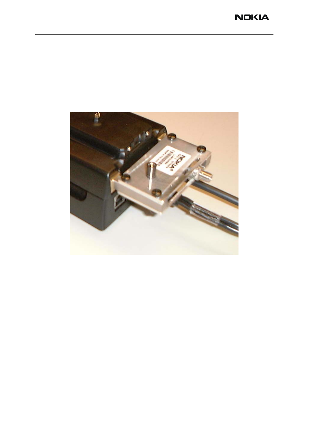
Galvanic Contact (GAC-2)
Galvanic Contact GAC-2 adapter provides an RF galvanic connection to RF test and measuring equipment.
Product Code
Galvanic Contact GAC-2 0770379
View of Galvanic Contact
Page 6 ãNokia Corporation Issue 1 11/02
Page 7
RH-13
CCS Technical Documentation Service Tools
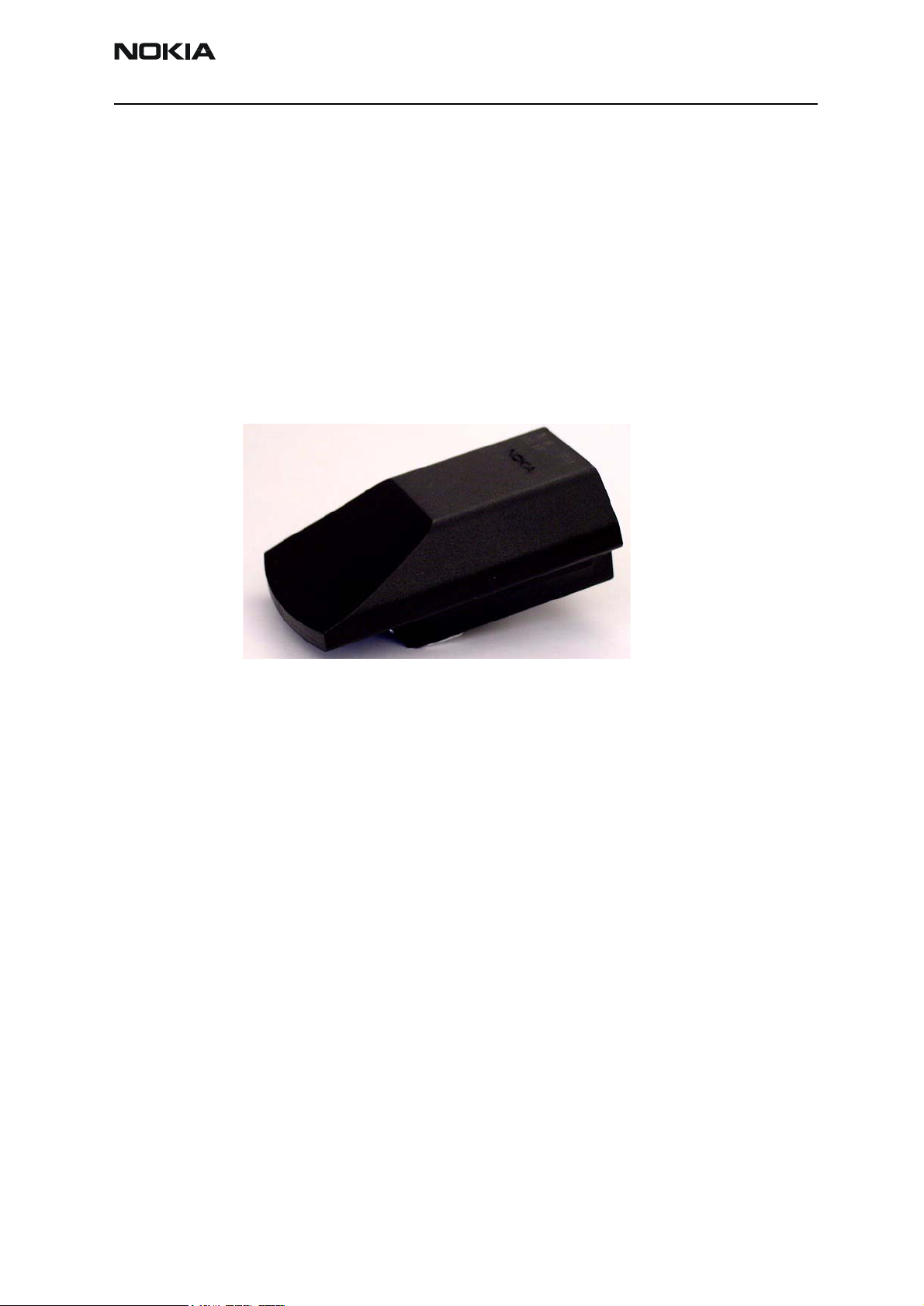
Flash Adapter (FLA-14)
Flash Adapter allows continuous maximum power supply for the phone from an external
power supply (FLS-4S or FPS-8). The flash adapter allows Mbus/Fbus connections. The
flash adapter is protected against over-voltage, over-current, and cross-connection. The
flash adapter provides a regulated voltage to the phone.
Note: The flash adapter is designed for flashing only.
Product Code
Flash Adapter FLA-14 0770293
with power cable 0080538
View of Flash Adapter
Issue 1 11/02 ãNokia Corporation Page 7
Page 8
RH-13
Service Tools CCS Technical Documentation
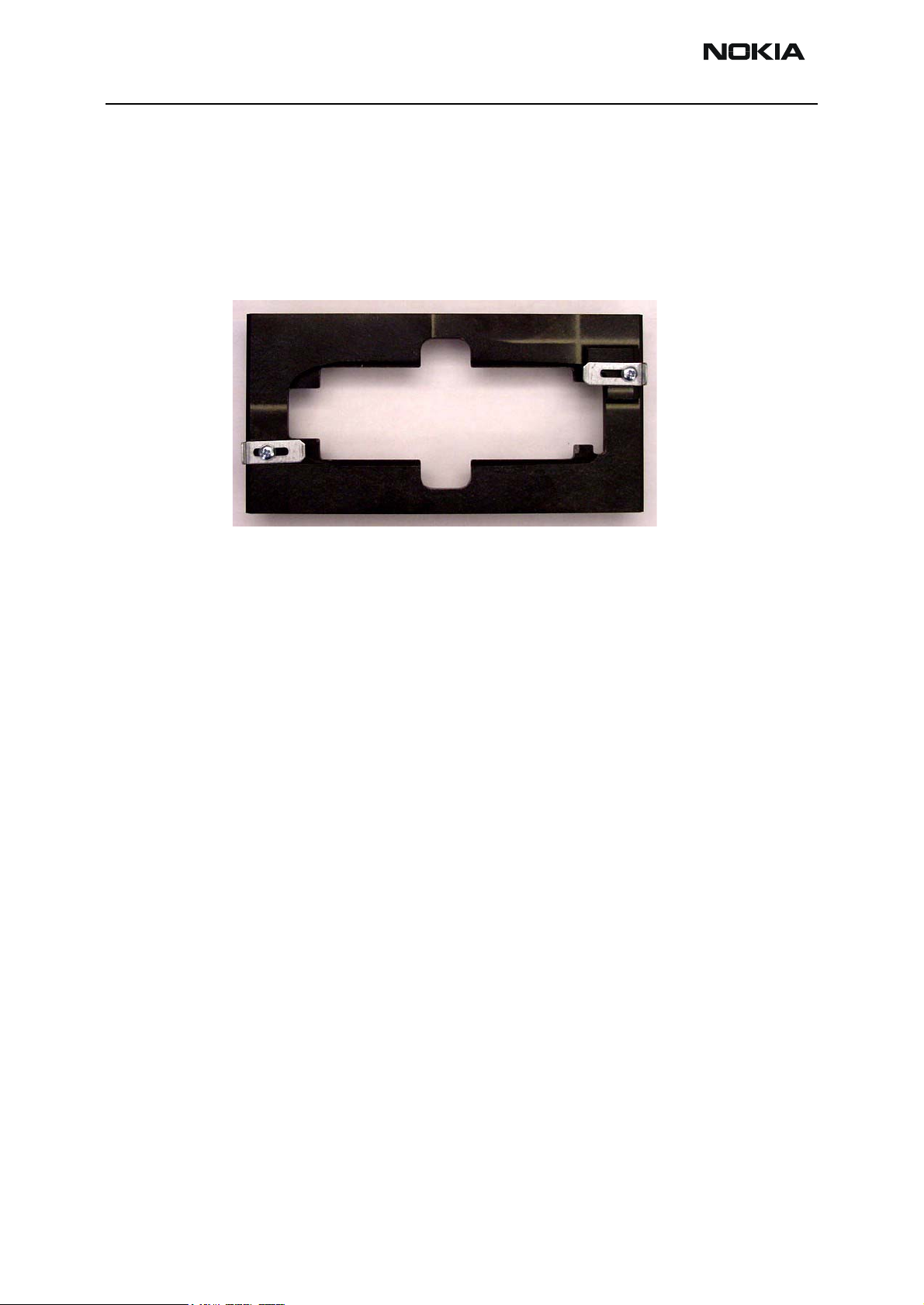
Soldering Jig (MJS-26)
The Soldering Jig is designed to hold PWB during repair and troubleshooting.
Product Code
Soldering Jig MJS-26 0770352
View of Soldering Jig
Page 8 ãNokia Corporation Issue 1 11/02
Page 9
RH-13
CCS Technical Documentation Service Tools
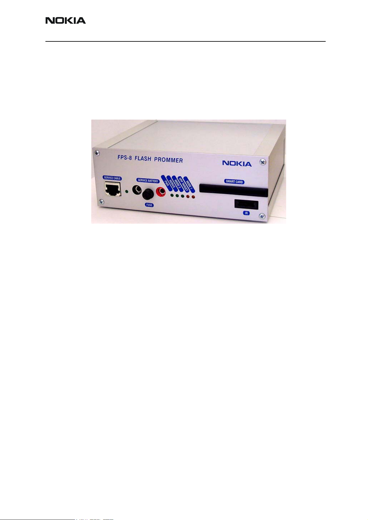
Flash Prommer (FPS-8)
The Flash Prommer FPS-8 is used for heavy flash.
Product Code
Flash Prommer FPS-8 0080321
View of Flash Prommer
Issue 1 11/02 ãNokia Corporation Page 9
Page 10
RH-13
Service Tools CCS Technical Documentation
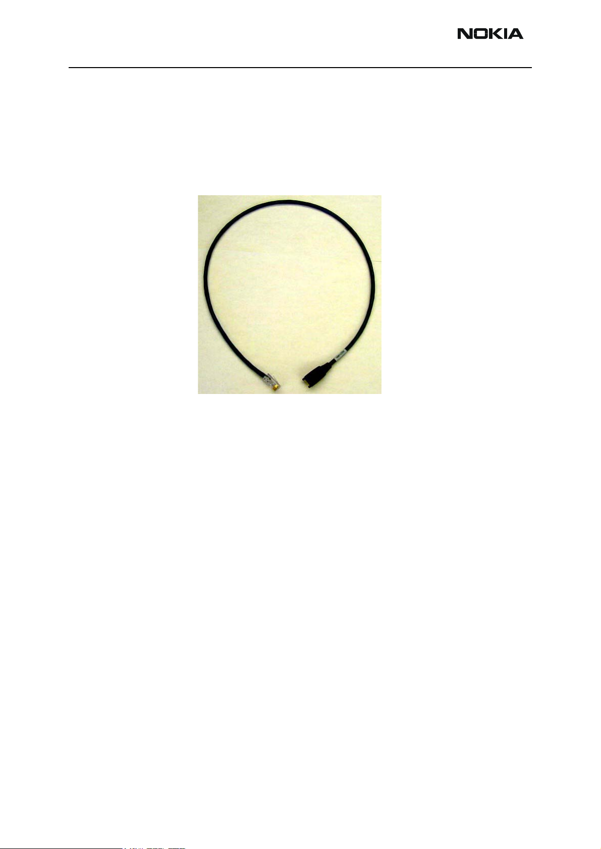
Audio Cable (ADS-6)
The Audio Cable connects to the Audio Box JBA-8.
Product Code
Audio Cable ADS-6 0730241
View of Audio Cable
Page 10 ãNokia Corporation Issue 1 11/02
Page 11
RH-13
CCS Technical Documentation Service Tools
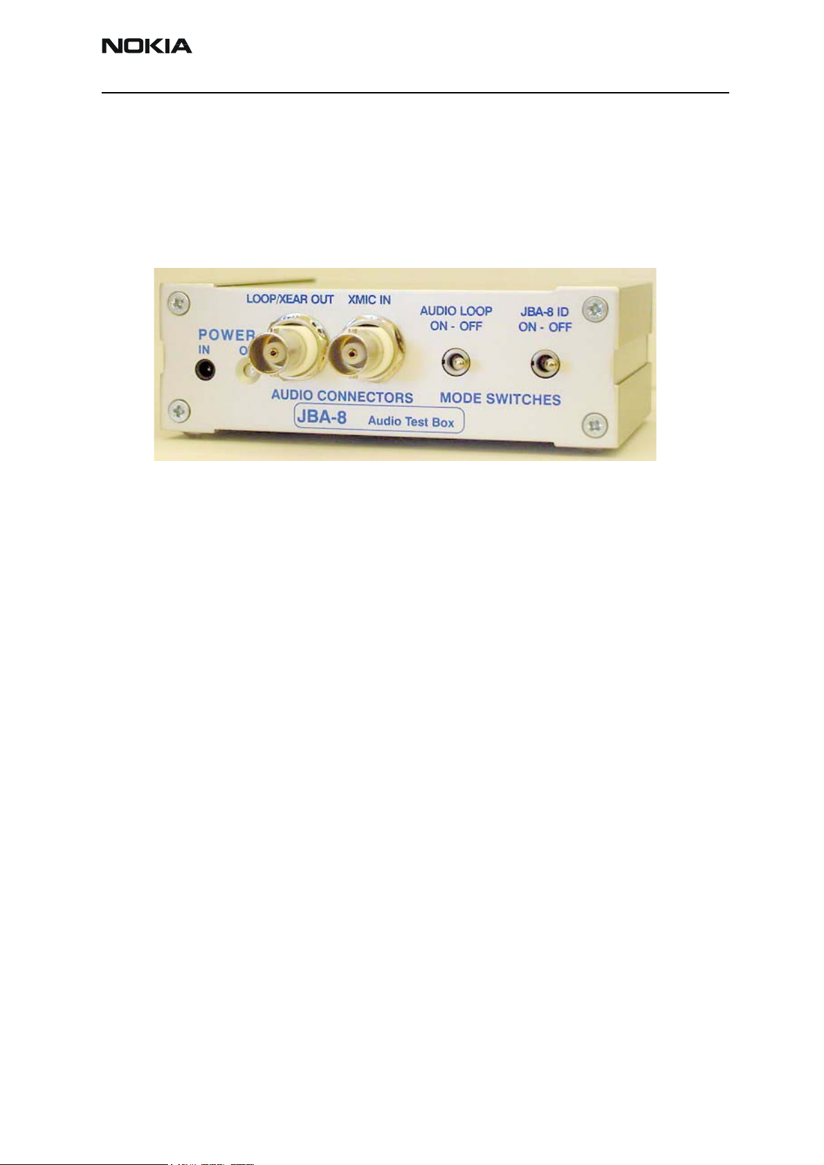
Audio box (JBA-8)
The JBA-8 is required for audio testing.
Product Code
Audio Box JBA-8 0770320
View of Audio Box
Issue 1 11/02 ãNokia Corporation Page 11
Page 12
RH-13
Service Tools CCS Technical Documentation
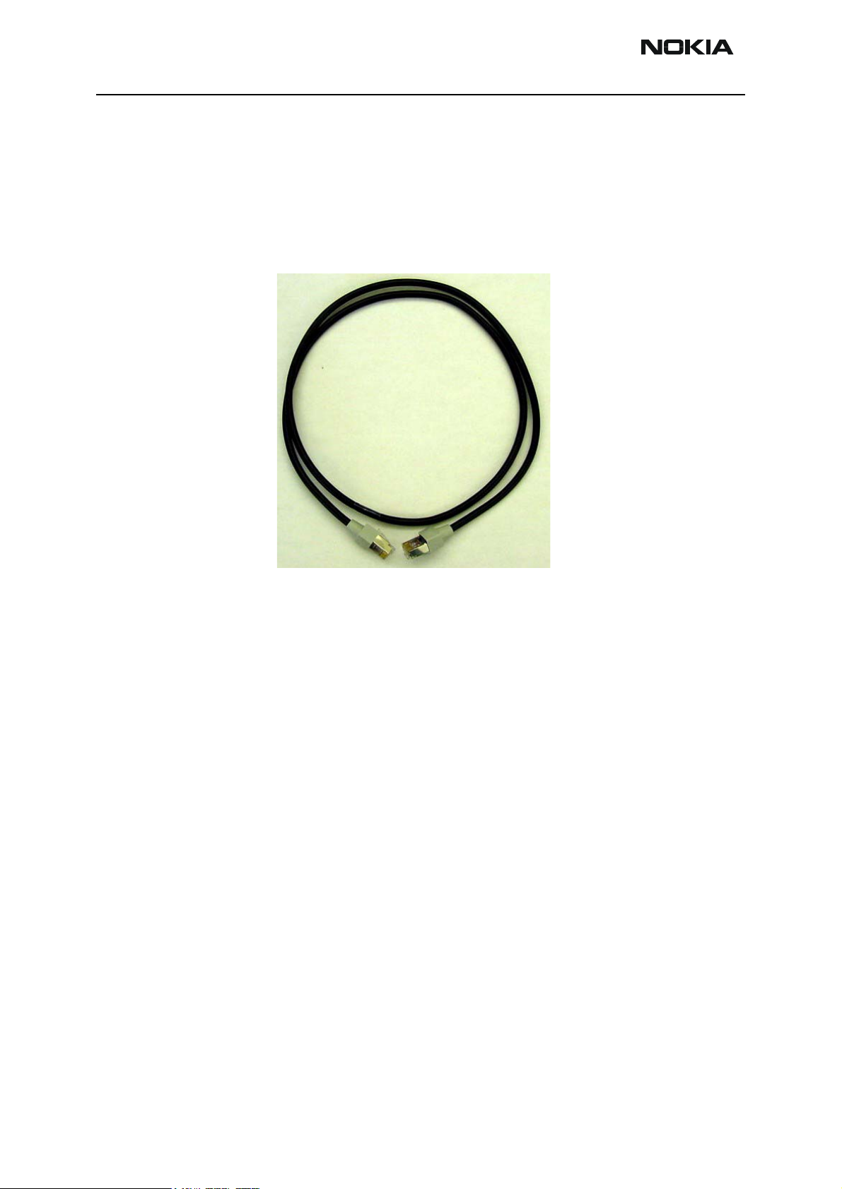
Mbus/Fbus Cable (XCS-4)
The XCS-4 Service Cable is a modular cable for flashing DCT4 products.
Product Code
Mbus/Fbus Cable XCS-4 0730178
View of Mbus/Fbus Cable
Page 12 ãNokia Corporation Issue 1 11/02
Page 13

RH-13
CCS Technical Documentation Service Tools
DC Cable (CA-5S)
The DC Cable CA-5S is used to connect the docking station to the charger connection
(Vin) of the phone to conduct the charger calibration service procedure.
Product Code
DC Cable CA-5S 0730283
View of DC Cable
Issue 1 11/02 ãNokia Corporation Page 13
Page 14

RH-13
Service Tools CCS Technical Documentation
Power Cable (PCS-1)
The Power Cable PCS-1 is used to connect the service tools (JBV-1, MJS-17) to an external power supply.
Product Code
Power Cable PCS-1 0730012
View of Power Cable
Page 14 ãNokia Corporation Issue 1 11/02
Page 15

RH-13
CCS Technical Documentation Service Tools
RF Cable (XRF-1)
RF Cable XRF-1 is used to connect the service tools to RF measuring equipment.
Product Code
RF Cable XRF-1 0730085
View of RF Cable
Issue 1 11/02 ãNokia Corporation Page 15
Page 16

RH-13
Service Tools CCS Technical Documentation
SW Security Device (PKD-1)
SW security device PKD-1 is hardware device that, when connected to the parallel (LPT)
port of the PC, enables the use of the service software. Without the dongle present, it is
not possible to use the service software. Printers or other peripheral devices can be connected to the PC through the dongle, if needed.
Caution: Make sure that you have switched off the PC and the printer before making connections!
Caution: Do not connect the PKD-1 to the serial port. You may damage your PKD-1!
Product Code
SW Security Device PKD-1 0750018
View of SW Security Device
Page 16 ãNokia Corporation Issue 1 11/02
Page 17

RH-13
CCS Technical Documentation Service Tools
Power Pack (DDC-10)
The Power Pack is designed to provide the phone with power via the FLA-14.The phone’s
own battery can be used in the DDC-10.
Note: DDC-10 allows battery charging. When it is used as a charger, the power pack need to be disconnected.
Note: When DDC-10 is used as a Power Pack, battery charging is not allowed!
Product Code
Power Pack DDC-10 0670405
View of Power Pack
Note: Do not plug cable into the charger receptacle.
Issue 1 11/02 ãNokia Corporation Page 17
Page 18

RH-13
Service Tools CCS Technical Documentation
Module Jig (MJS-17)
This jig allows phone PWB level service and troubleshooting.
Product Code
Module Jig MJS-17 0770353
View of Module Jig
Page 18 ãNokia Corporation Issue 1 11/02
Page 19

RH-13
CCS Technical Documentation Service Tools
Parallel Flash Prommer (FPS-8C)
The FPS-8C Flash Prommer is used for heavy parallel flashing.
Product Code
Parallel Flash Prommer FPS-8C 0080396
View of Parallel Flash Prommer
Issue 1 11/02 ãNokia Corporation Page 19
Page 20

RH-13
Service Tools CCS Technical Documentation
POS Flash (FLS-4S)
The Point of Sale (POS) flash is a low-cost software upgrade tool. This requires the XCS-1
cable and ACF-8 for operation.
Product Code
FLS-4S Sales Package for Americas 0080543
APAC 0080542
Europe/Africa 0080541
View of POS Flash Adapter
Page 20 ãNokia Corporation Issue 1 11/02
Page 21

RH-13
CCS Technical Documentation Service Tools
MBUS Cable (DAU-9P)
The MBUS cable DAU-9P provides a connection from the serial port of the computer to
the system connector of the phone.
Product Code
MBUS Cable DAU-9P 0272034
View of MBUS Cable DAU-9P
Issue 1 11/02 ãNokia Corporation Page 21
Page 22

RH-13
Service Tools CCS Technical Documentation
MBUS Cable (DAU-9S)
The MBUS Cable DAU-9S has a modular connector and is used with the service Audio
Box JBA-8.
Product Code
MBUS Cable DAU-9S 0730108
View of MBUS Cable DAU-9S
Page 22 ãNokia Corporation Issue 1 11/02
Page 23

RH-13
CCS Technical Documentation Service Tools
Printer Cable (AXP-8)
The Parallel Printer Cable connects the parallel connector of the PC and the parallel input
of the FPS-8 or FPS-8C.
Product Code
Printer Cable AXP-8 073F000
View of Printer Cable
Issue 1 11/02 ãNokia Corporation Page 23
Page 24

RH-13
Service Tools CCS Technical Documentation
Modular T-adapter
The Modular T-adapter is a suitable branching unit to provide the needed parallel modular connections.
Product Code
Modular T-adapter 4626134
View of Modular T-adapter
Page 24 ãNokia Corporation Issue 1 11/02
Page 25

RH-13
CCS Technical Documentation Service Tools
Gait Test SIM card
Service point GAIT Test SIM to be used in connection with the RH-13 handset.
Product Code
Gait Test SIM card 0750190
View of Gait Test SIM card
Issue 1 11/02 ãNokia Corporation Page 25
Page 26

RH-13
Switch2
Switch3
Service Tools CCS Technical Documentation
Module Jig MJS-17 0770353
Introduction
Module Jig MJS-17 is designed for regional Central Services for engine testing. It can be
used for flashing and RF, battery, system, SIM reader. The MJS-17 sales pack includes all
the needed modification parts for RH-13. The MJS-17 is equipped with over current, over
voltage and voltage polarity -protection.
List of modules
Table 1: List of modules
Name of module NMP code Material code Notes
Module service jig MJS-17
0770353
Module service jig to R&D and testing environment
Technical Specifications
Electrical characteristics
Table 2: Electrical ratings
Parameter Min Nom Max Notes
Supply voltage 3.0V 5.0V Abs.Max.10V!
Vbatt 3.0V 3.9V 4.2V
Vbat current 2.0A
Vbat current 2A
BTEMP
Local mode
Normal mode
BSI
Local mode
Normal mode
560R
47k
560R
68k
switch 3
switch2
BSI à FPS8 ON/OFF switch1
Figure 1: Switches
Switch1
Page 26 ãNokia Corporation Issue 1 11/02
Page 27

RH-13
CCS Technical Documentation Service Tools
Testing
Recommended Test Equipment
1 Power supply
2Scope
3 Multimeter
4 Network analyzer
Test Procedure
1 Check visually that all mechanical parts are well placed and properly fixed
together
2 Check that Vbatt-line wakes when supply voltage is 3.2 V ±2%
3 Check that Vbatt-line shuts down when supply voltage is 4.2 V ±2%
4 Measure XRS-2 RF-cable attenuation:
•900 MHz 0.2dB +-0.1dB
•1800 MHz 0.3dB +-0.1dB
•1900 MHz 0.4dB +-0.1dB
User Instructions
General instruction
Note: MJS 17 is manufactured out of a very spaltible material,Trespa Athlon. DO
NOT HANDLE ROUGHLY.
Warning: The absolute maximum supply voltage is 10 V (recommended 5V). Higher
voltages will destroy the Module Jig.
Operation
1 Open module jig by pressing the button on the cover and lift the cover from the
finger –cutting.
2 Put pcb engine through it´s corner holes to alignment pins on the base of the
module jig.
3 NOTE! PCB MUST BE SET TO IT´S PLACE FULLY DOWNRIGHT!
4 Close the module jig by pressing the cover until the lock “clicks”.
5 Connect modular cable XMS-3 to modular connector of MJS 17.
6 Adjust supply voltage to 3.0 – 4.2 V.
Note: Before adjusting the power supply, make sure that the MJS-17 is connected to the ground.
7 Connect DC –plug to DC –jack of MJS 17.
8 Connect RF –cable to RF-connector (item 7) of the MJS 17.
9 If used the pcb with lightguide and LCD –module, you can put the keymat film to
it´s position on the engine.
10 Use a probe to test the components of the engine.
Over current and voltage
The Module Jig has overcurrent protection (2A fuse). Over current protection activates if
the Vbatt-line is overloaded.
Issue 1 11/02 ãNokia Corporation Page 27
Page 28

RH-13
SIM PWB
Service Tools CCS Technical Documentation
Do not use higher supply voltage than 5V. If absolute maximum supply voltage 10V is
exceeded, tantalum capacitors in supply line (V+) will be damaged and MJS 17 is permanently out of use.
Assembly
Construction
Figure 2: MJS-17 closed
Figure 3: Fuse, RF connector and SIM pwb
FUSE
RF Connector
XRS-2
Changeable parts
Table 3: Changeable electrical parts
Item Qty
33 1 MEK1 T2A Slow fuse Fuse 5x20mm na Bussmann
35 11 MEK3-
Referen
ce
MEK12
Value Model Description
1.5A GKS-079301050A1300 Probe for KS-07935 ref (1 Ingun
NMP
code
MFG
1) available only as 10 pcs sales pack 0770488
Table 4: Changeable mechanical parts
Item Qty Description Drawing number NMP code Supplier
2 1 Alignment pin right 99EM005E ref (2 Oulun hienomek
3 1 Alignment pin left 99EM006D ref (2 Oulun hienomek
4 1 Alignment pin (MJS-17 L/C) right 1AZM001A ref (2 Oulun hienomek
5 1 Alignment pin (MJS-17 L/C) left 00NM003D ref (2 Oulun hienomek
1 Sim module ref (2 PKC
7 1 XRS-2 RF connector MZ 0730182 Sorv-elektro
Page 28 ãNokia Corporation Issue 1 11/02
Page 29

RH-13
right pin
left pin
Item 2
Item 3
CCS Technical Documentation Service Tools
2) available as a kit only; MJS-17K spare part kit for MJS-17, code 0770495
Modifications of MJS-17 for RH-13
The sales package includes all the needed components for preparing the jig for RH-13
Figure 4: Parts needed for RH-13.
3.NPM-2NX
Item 5
Change of Alignment pins
2
.NPM-2NX
SIM Module
Figure 5: Pin storage
Item 6
Item 4
Item 1
Step 1: Open two screws by torx screwdriver (tx6) behind in the bottom of the jig.
Step 2: Take aligning pins 4 and 5 out of slot.
Step 3: Unscrew aligning pins 2 and 3 carefully using pliers. Use thin board or rubber
plate between pliers and aligning pins to avoid disturbing surface of the pins.
Step 4: Screw new aligning pins 4 and 5 (for NPW-2/NHP-2NX/NHP-2FX/RH-13) to the
same place using the same pliers.
Note the order of the pins!
Figure 6: Unscrewed aligning pins
Step 5: After changing the pins, put RH-13 alignment pins (items 2 and 3) back to slot
behind the Base, item 1.
Issue 1 11/02 ãNokia Corporation Page 29
Page 30

RH-13
Remove SIM
Fasten SIM Module
Service Tools CCS Technical Documentation
SIM Module pwb
Step 1: Screw three torx screws of SIM Module pcb and take the pcb out of MJS-17.
Step 2: Fix the pcb to its place in Cover (item 12).
Figure 7: Opened SIM Module pcb
Open 3 screws (TX6)
Module
Figure 8: SIM Module stored in cover
into cover
Changing the test pins
Pulling the test pins out of pwb
Pull the test pins out from pwb 1 by using thin sharpness pliers.
Note: Make sure you take hold of the right place on the test pins. Do not take hold of
the lowest part ofthe test pins to avoid disturbing the base of test pins.
Figure 9: Changing the test pins
Figure 10: Contact with the test pin
Right place to hold
pinwithpliers
Page 30 ãNokia Corporation Issue 1 11/02
Page 31

RH-13
CCS Technical Documentation Service Tools
Docking Station Adapter MJF-1 0770354
Introduction
The MJF-1 docking station adapter has been designed for Services for calibration and
software update use. It is used with Docking station JBV-1. MJF-1 makes signal connections to the transceiver. The Docking station adapter MJF-1’s main electronics functions
are:
• Phone recognizing from BTEMP
• Filters of FBUS – signals
List of Modules
Table 5: List of modules
Name of Module NMP code Material code Notes
Docking station adapter MJF-1 0770354 Docking station adapter to AMS usage
Technical Specifications
DC Characteristics
Table 6: Electrical ratings
Parameter Min Nom Max
Recognizing voltage from BTEMP 0,108V 0,111V 0,114V
D- Connector signals
D-connector (male) is between MJF-1 and JBV-1.
Issue 1 11/02 ãNokia Corporation Page 31
Page 32

RH-13
Service Tools CCS Technical Documentation
Figure 11: D-connector signals
VBATT 1
14 VBATT_SENSE
VBATT 2
15 DC+
DC+ 3
16 +COUP
NC 4
17 NC
NC 5
18 NC
NC 6
19 NC
NC 7
20 NC
PHONE_RECOGNIZING 8
21 BTEMP
BSI 9
22 FBUS/TX
FBUS/RX 10
23 MBUS
GND(BUS) 11
24 VPP
GND 12
25 GND_SENSE
GND 13
Table 7: D-connector signal descriptin
PIN Signal Description Min Max
1,2 VBATT Battery voltage to phone 3.0V / 0A 5.0V / 1.5A
2 VBATT
3, 15 DC+ Supply voltage to JBV-1
4 NC Not connected
5 NC Not connected
6 NC Not connected 0
7 NC Not connected
8 PHONE_RECOGNIZING Phone recognizing from jig. Active low 0 +coup ( 3.3V)
9 BSI BSI signal from phone
10 FBUS/TX FBUS TX signal from modular connector
11 GND(BUS) GND from modular connector. Not connected to
battery GND on JBV-1
12,13GND Battery voltage GND
14 VBATT_SENSE Battery voltage sense. Used for regulator voltage
feedback
16 +COUP Coupler voltage 3.0V 3.3V
17 NC Not connected
18 NC Not connected
Page 32 ãNokia Corporation Issue 1 11/02
Page 33

RH-13
CCS Technical Documentation Service Tools
19 NC
20 NC
21 BTEMP BTEMP signal from phone
22 FBUS/RX FBUS RX signal from modular connector
23 MBUS MBUS signal from modular connector
24 VPP VPP signal from modular connector
25 GND_SENSE Battery gnd sense Used for regulator voltage feed-
back
Mechanical Characteristics
Table 8: Mechanical characteristics
Unit
MJF-1 71.5 x 36.8 x 119,6 150 ABS/PC, Cycoloy C1000F Color. 76701 Black
Dimensions (mm)
(W x H x D)
Weight (g) Material
Figure 12: MJF-1 main dimensions
Environmental Conditions
Temperature Conditions
Table 9: Allowed ambient temperatures
Ambient Temperature (degrees Celcius)
Operating temperature +5…+35
Storage temperature -30…+60
Humidity RH Max. 90%
Testing
Recommended Test Equipment
1 Power supply
2 Multimeter
Test Procedure
1 Make visual check that all mechanical parts are well placed and properly fixed
Issue 1 11/02 ãNokia Corporation Page 33
Page 34

RH-13
Service Tools CCS Technical Documentation
together
2 Check that PHONE_RECOGNIZING-line activate when BTEMP voltage is 0.17
3 Check FBUS / MBUS filters
User Instructions
General instruction
NOTE: Be careful with pins. Especially if you change them or open the jig.
Operation
Normal:
1 Check that all pins and small pcb are OK.
2 Set MJF-1 to JBV-1 by pushing it`s dowel pins to JBV-1 holes.
3 Best way to assemble a phone into jig is put the phone`s battery spring side first
to the jig and then other side.
Over current and voltage
MJF-1 don’t have over voltage or over current protection. All protection devices are in
JBV-1.
Assembly
Construction
Figure 13: MJF-1 assembled with JBV-1
Changing the test pins to MJF-1
Step 1. Opening the MJF-1 cover.
Open the screws using the TX6 chisel and open the MJF-1 cover with the chisel.
Figure 14: Opening the MFJ-1 cover.
Step 2. Take away the pwb 1
Page 34 ãNokia Corporation Issue 1 11/02
Page 35

RH-13
CCS Technical Documentation Service Tools
Open the screws by the chisel and take the pwb out of MJF-1.
Figure 15: Taking away the pwb 1
Step 3. Pulling the test pins out of pwb
Pull test pins from pwb 1 by using thin sharpness pliers.
Note: Make sure you take hold of the right place on the test pins. Do not take hold
of the lowest part of the test pins to avoid disturbing base of the test pins. The best
place is the middle of the top location of the test pins. From here, it will be successful to change the pins.
Figure 16: Pulling the test pins out of the pwb
Step 4. Adding the pwb into the MJF-1
Locate pwb 1 carefully to the MJF-1 focusing the right adjustment with the test
pins. Push by using your finger the pwb 2 to the MJF-1’s hole.
Figure 17: Adding the pwb into the MFJ-1
Step 5. Adding cover into MJF-1
Fasten screws using the TX6 chisel
Issue 1 11/02 ãNokia Corporation Page 35
Page 36

RH-13
Service Tools CCS Technical Documentation
Flash Adapter FLA-14 0080538
Introduction
Flash adapter FLA-14 is designed for regional Central Services and POS (Point of Sales) to
replace phones own battery when flashing the phone. The FLA-14 contains three protections:
• Over current protection
• Over voltage protection
• Voltage polarity protection
List of Modules
Table 10: List of modules
Name of modules NMP type NMP code Notes
Flash adapter FLA-14 0770293 Flash adapter to AMS usage
Technical Specifications
DC Characteristics
Table 11: Electrical ratings
Parameter Min Nom Max Notes
Input voltage (charger) 5.5V - 16V
Supply voltage (power supply) 3.0V - 4.2V (16V) *)
Vbatt (charger) 3.8V 3.9V 4.1V Regulated
Vbatt (power supply) 3.0V - 4.2V No regulation
Vbatt current (charger) 210mA - 300mA Rejected
Vbat protection current 2A Resettable fuse
BTEMP
Local mode
Normal mode
BSI
Local mode
Normal mode
560R
47k
560R
68k
Resistor
Resistor
*) Absolutely maximum value, do not exceed.
Modes of operation
Flash adapter FLA-14 can be used in two operation modes:
• Normal mode (input voltage 3.0 – 4.2V)
• Local mode for flashing (input voltage 5.5 – 16V)
Page 36 ãNokia Corporation Issue 1 11/02
Page 37

RH-13
CCS Technical Documentation Service Tools
Mechanical Characteristics
Table 12: Mechanical characteristics
Unit Dimensions (mm) (W x H x D) Weight (g) Material
FLA-14 45.5x32.8x76.4 75 ABS/PC, Cycoloy C1000F
Figure 18: Main dimensions of FLA-14
Environmental Conditions
Temperature Conditions
Table 13: Allowed ambient temperatures
Ambient temperature (degrees Celcius)
Operating temperature +5…+35
Storage temperature -30…+60
Humidity RH Max. 90%
Functional Description
Circuit Description
In Normal mode, when 3.0 – 4.2V supply voltage is used, the output voltage windowing
circuit controls the FET-transistor V1, which passes 3.0 – 4.2V to the VBATT line. In Local
mode, when using the 5.5 – 16V supply voltage, the regulator N1 is enabled and the 4.1V
regulated voltage is leaded to the VBATT line. The current is limited in Local Mode to 210
– 300mA. Led D3 indicates the used operation mode. Yellow light for 3.0 – 4.2V and
green for 4.1V regulated voltage. Two auto switches are accomplished by bipolar NPN
transistors. Resistor values for BSI and BTEMP line in Local mode are 560 Ohms and in
Normal mode 68 / 47 kOhms.
Flash adapter has an over current protection (resettable fuse). It activates when VBATTline is over loaded. Operation will be normalized automatically after supply voltage is
switched off or fault condition is removed.
Testing
Recommended Test Equipment
1 Power supply
Issue 1 11/02 ãNokia Corporation Page 37
Page 38

RH-13
Service Tools CCS Technical Documentation
2Scope
3 Multimeter
4 DC current loads 1.5A and 300mA
Test Procedure
1 Check visually that all mechanical parts are well placed and properly fixed
together
2 Check that Vbatt-line is shut when supply voltage is less than 2.9 V
3 Check that Vbatt-line wakes up when supply voltage is 3.0 V ±2%
4 Check that the indicator led is yellow
5 Check that BSI resistance 68k
6 Check that BTEMP resistance is 47k
7 Check that Vbatt-line shuts down when supply voltage has risen up to 4.2 V ±2%
8 Check that Vbatt-line (4.1 V ±2%) wakes up when supply voltage is over 5.5V
9 Check that the indicator led is green
10 Check that BSI and BTEMP resistances are 560 Ohms
11 Check the current limitation; Vbatt-line shuts down when current is between
210– 350 mA (supply voltage 10 V)
12 Check that total resistance value in FBUS TX/RX filter lines is 940Ω ±1%
13 Check that total resistance value in MBUS filter line is 94Ω ±1%
User Instructions
General instruction
Note: Be careful with the pins, especially if you change them or open the jig.
Operation
Normal:
1 Check that all pins and small pcb are OK.
2 Best way to assemble a phone into jig is put the phone`s battery spring side first
to the jig and then other side.
Assembly
Construction
Figure 19: FLA-14 top view
Changing the test pins to FLA-14
Step 1. Opening the FLA-Acover2
Page 38 ãNokia Corporation Issue 1 11/02
Page 39

RH-13
CCS Technical Documentation Service Tools
Open the FLA-Acover2 by using a chisel. Push the chisel carefully between FLAAcover2 and FLA-Bcover. Open the FLA-Acover2 prising the chisel.
Figure 20: Opening the FLA-Acover2
Step 2. Taking pwb 1 out of front cover
Using the same chisel, push the pwb 2 down and pull using your other hand pwb1
rid of FLA-Bcover.
Step 3. Gripping pins from pcb 1
Pull test pins from pwb 1 by using thin sharpness pliers.
Note: Make sure that you take hold of the right place on the test pins. Do not
take hold of the lowest part of the test pins to avoid disturbing the base of
the test pins. The best place is the middle of the top location of the test
pins. This way, you will be successful in changing the pins.
Step 4. Fastening the pcb to the FLA-Bcover
Locate pwb 1 carefully to the FLA-Bcover focusing the right adjustment with the
test pins. Push the pwb 2 to the FLA-Bcover’s hole with your finger. Push pwb 2
carefully vertical to the FLA-Bcover.
Figure 21: Fastening the pcb to the FLA-Bcover
Step 5. Fastening the FLA-Acover2 to the FLA-Bcover.
Pull carefully the FLA-Bcover in to the FLA-Acover2.
Issue 1 11/02 ãNokia Corporation Page 39
Page 40

RH-13
Service Tools CCS Technical Documentation
This page intentionally left blank.
Page 40 ãNokia Corporation Issue 1 11/02
 Loading...