

Page 1

CCS Technical Documentation
RH-13 Series Transceivers
System Module
Issue 1 11/02 ãNokia Corporation
Page 2

RH-13
System Module CCS Technical Documentation
Contents
Page No
Abbreviations................................................................................................................. 5
Transceiver RH-13......................................................................................................... 7
Introduction ..................................................................................................................7
Engine Module WG8 ..................................................................................................... 8
Introduction ..................................................................................................................8
UEM ............................................................................................................................8
UEM introduction ..................................................................................................... 8
Blocks........................................................................................................................ 9
RF IF ....................................................................................................................... 10
Charging Control..................................................................................................... 10
DIGITAL IF............................................................................................................ 11
AUDIO CODEC ..................................................................................................... 11
UI DRIVERS........................................................................................................... 11
IR interface.............................................................................................................. 11
AD CONVERTERS................................................................................................ 11
SIM.......................................................................................................................... 11
Technical information ............................................................................................. 11
UPP ............................................................................................................................12
Introduction............................................................................................................. 12
Blocks...................................................................................................................... 12
Technical information ............................................................................................. 12
Flash memory ............................................................................................................12
Introduction............................................................................................................. 12
Technical information ............................................................................................. 12
UIHW ........................................................................................................................13
LCD......................................................................................................................... 13
Audio HW ..................................................................................................................17
Earpiece................................................................................................................... 17
Microphone ............................................................................................................. 18
Buzzer...................................................................................................................... 18
Battery ........................................................................................................................19
Phone battery........................................................................................................... 19
Battery connector .................................................................................................... 20
Accessories Interface .................................................................................................20
System connector .................................................................................................... 20
IR module................................................................................................................ 21
Charger IF ............................................................................................................... 22
Data cable................................................................................................................ 23
Test interfaces ............................................................................................................23
Production test pattern............................................................................................. 23
Other test points ...................................................................................................... 24
EMC ...........................................................................................................................24
General .................................................................................................................... 24
BB component and control/IO line protection........................................................ 25
Transceiver interfaces ................................................................................................27
BB - RF Interface Connections ..................................................................................27
BB Internal connections ............................................................................................30
Page 2 ãNokia Corporation Issue 1 11/02
Page 3

RH-13
CCS Technical Documentation System Module
UPP Block signals................................................................................................... 36
MEMORY Block Interfaces.................................................................................... 41
IR Block Interfaces.................................................................................................. 42
SIM Block Interfaces .............................................................................................. 42
Audio Interfaces ...................................................................................................... 43
Key/Display blocks ................................................................................................. 45
Baseband External Connections ................................................................................46
Test Pattern for production tests.............................................................................. 48
General about testing .................................................................................................48
RF Module ................................................................................................................... 50
Introduction ................................................................................................................50
Requirements........................................................................................................... 50
Design...................................................................................................................... 50
Interfaces ....................................................................................................................50
Environmental Specifications ....................................................................................51
Temperature Conditions.......................................................................................... 51
Vibration and Free Fall ........................................................................................... 51
Humidity and Water Resistance.............................................................................. 52
ESD strength ........................................................................................................... 52
Main Technical Specifications ..................................................................................52
RF frequency plan ................................................................................................... 52
DC Characteristics................................................................................................... 54
Functional Description ...............................................................................................55
Block diagram ......................................................................................................... 55
Receiver................................................................................................................... 56
Frequency Synthesizers........................................................................................... 57
Transmitter.............................................................................................................. 57
Software Compensations......................................................................................... 58
RF Characteristics ......................................................................................................59
Receiver................................................................................................................... 60
Transmitter.............................................................................................................. 61
Synthesizers............................................................................................................. 62
Antenna ................................................................................................................... 63
EMC........................................................................................................................ 63
Radiated spurious emissions, Receiver................................................................... 63
Conducted spurious emissions, Receiver................................................................ 63
Harmonic and spurious emissions, Transmitter, conducted and radiated............... 64
Maintainability ...........................................................................................................64
Issue 1 11/02 ãNokia Corporation Page 3
Page 4

RH-13
System Module CCS Technical Documentation
List of Figures
Fig 1 RH-13 Block Diagram................................................................................................7
Fig 2 System Block Diagram...............................................................................................8
Fig 3 LCD interface ............................................................................................................13
Fig 4 Placement of keys.......................................................................................................14
Fig 5 SIM block...................................................................................................................17
Fig 6 Battery connection diagram........................................................................................19
Fig 7 BLB-3 Battery contacts (BLB-2 has the same interface)...........................................20
Fig 8 System connector........................................................................................................21
Fig 9 IR interface .................................................................................................................22
Fig 10 Top view of production test pattern..........................................................................24
Fig 11 Telescoping pattern between UPP and UEM ..........................................................24
Fig 12 Transceiver block naming for interfaces ..................................................................27
Fig 13 RH-13 Frequency Plan .............................................................................................53
Fig 14 Power Distribution Diagram.....................................................................................54
Fig 15 Block diagram of the RH-13 RF module ................................................................56
Page 4 ãNokia Corporation Issue 1 11/02
Page 5

RH-13
CCS Technical Documentation System Module
Abbreviations
ADC Analog to Digital Converter
ASIC Application Specific Integrated Circuit
BB Baseband
COG Chip On Glass
ENGINE The Transceiver parts fixed to PWB
FBUS Fast asynchronous serial bus
FDL Flash Down Loading, programming the phone FLASH memory
GSM Global system for mobile communications (Groupe Spêcial Mobile)
HW Hardware
I & Q In phase and Quadrature components of complex signal
IR Infrared. A wireless data/audio transmit medium.
IrDA Infrared Data Association
JTAG An in-circuit test method, based on the standard IEEE-1149.1
LDO Low Drop Out
LED Light Emitting Diode
Low Iq mode Low quiescent current mode
MBUS A bidirectional serial bus
NTC Negative Temperature Coefficient.
PWB Printed Wiring Board
PCM Pulse Code Modulation
PDM Pulse Density Modulation
PWM Pulse Width Modulation
RF Radio Frequency
Rx Receiver path
Issue 1 11/02 ãNokia Corporation Page 5
Page 6

RH-13
System Module CCS Technical Documentation
SIM Subscriber Identity Module
SW Software
TDMA Time Division Multiple Access
Transceiver Transmitter & Receiver, mobile phone
Tx Transmitter path
UEM Universal Energy Management baseband ASIC.
UI User Interface
UPP Universal Phone Processor baseband ASIC.
US United States (of America)
US-AMPS Analog Mobile Phone System used in United States
US-DAMPS Digital AMPS, used in US, channel compatible with AMPS
Page 6 ãNokia Corporation Issue 1 11/02
Page 7
RH-13
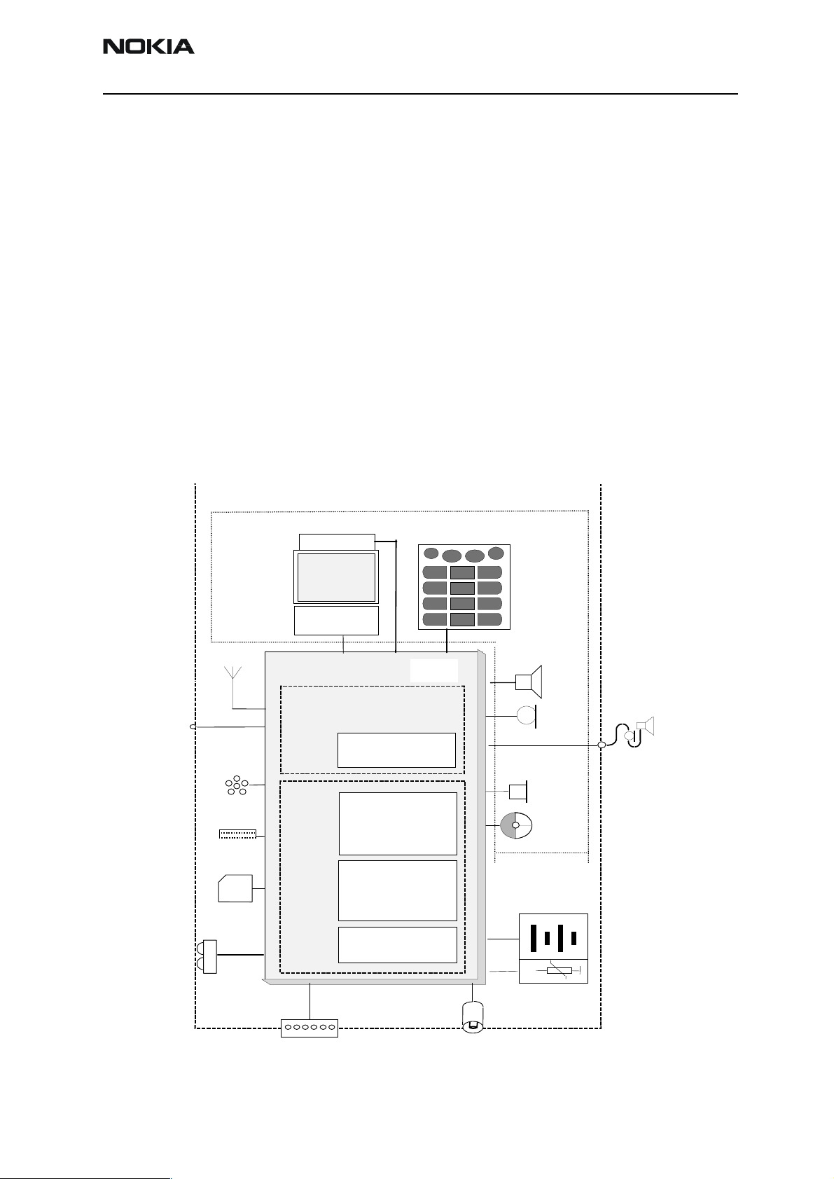
2
345
7
8
CCS Technical Documentation System Module
Transceiver RH-13
Introduction
The RH-13 is a dual band radio transceiver unit for GAIT (AMPS/TDMA800/GSM850/
TDMA1900/GSM1900) networks. It is a true 3 V transceiver with an internal antenna and
a vibra.
Mechanical construction resembles Nokia 61XX series and the same accessories can be
used. External RF connector is included.
An integrated Infrared link is located on the top of the phone.
RH-13 has the connection for the small SIM (Subscribe Identity Module) card.
The PWB has one-sided SMD and there is no separate User Interface PWB but the keyboard connections are on the non-SMD side of the board.
EXT RF
ANT
Test I/F
Ostrich
SIM
Figure 1: RH-13 Block Diagram
LCD DRIVER
✉
Display
Backlight/
Frontlight
System Module W G8
RF
800/1900 MHz
SAFARI_GTE
BB
UEM
RF Converters
Audio
Energy Managem ent
UPP8M
MCU:ARM7
DSP: LEAD3
System Logic
1
1AG
TRANSCEIVER
USER INTERFACE
☎
6
9
0#
EARP
HEADSET
MIC
BUZZER
VIBRA
BATTERY
BTemp
INFRA RED
Ext. Mem ory
~
~
~
~
SYSTEM
CONNECTOR
Flash-ROM 64 Mbit
CHARGING
Issue 1 11/02 ãNokia Corporation Page 7
Page 8
RH-13
V
Y
SIMCARD
SIMIF
System Module CCS Technical Documentation
Engine Module 1AG
Introduction
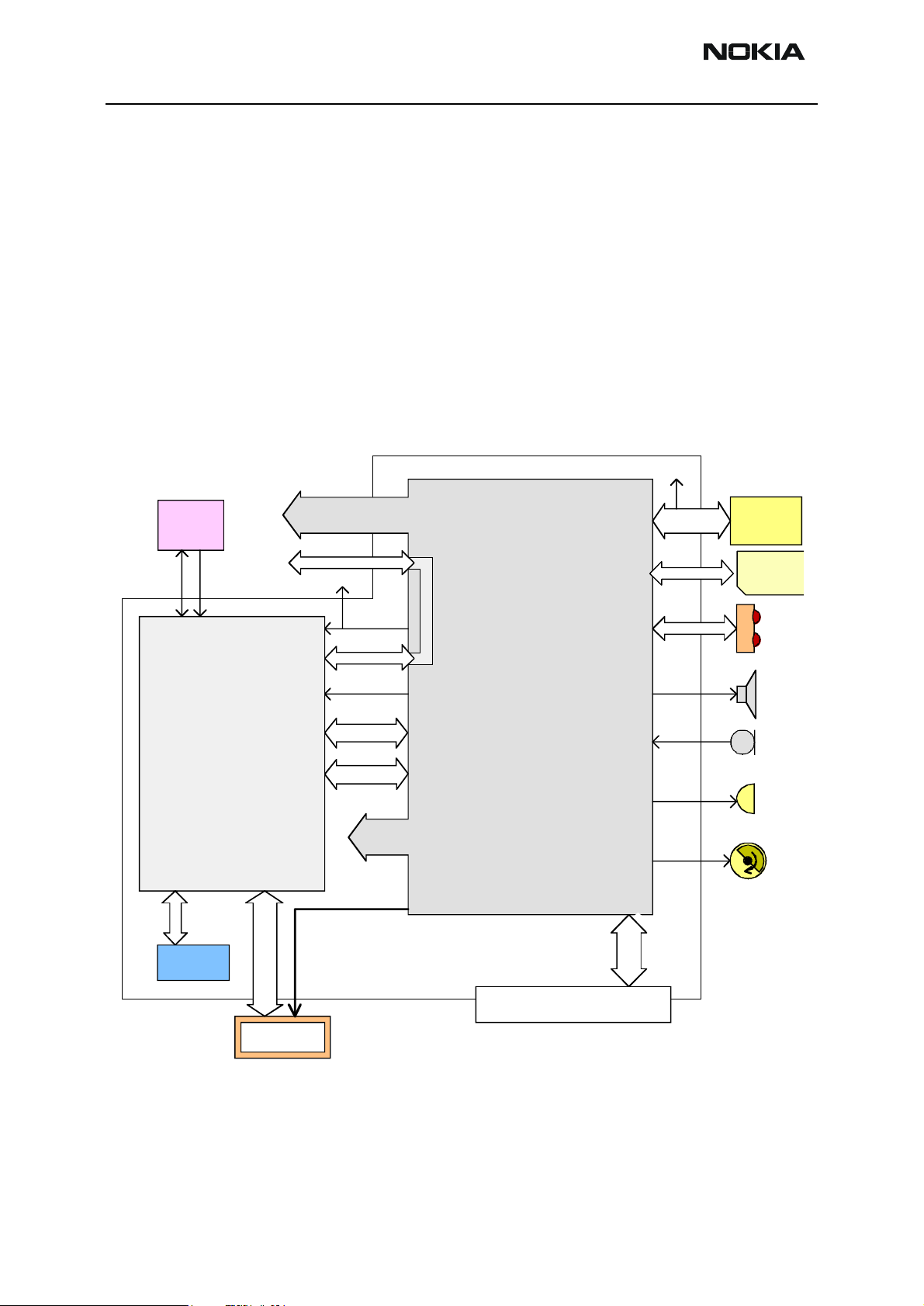
This section describes the baseband part of the RH-13 transceiver.
The BB architecture is similar to the earlier BB generation. The major difference is the
integration level. Core BB consists of 2 ASICs and flash memory.
BB core technical specification
The core part of RH-13 BB (figure below) consist of 2 ASICs, UEM and UPP, and flash
memory. Following sections describe these parts.
Figure 2: System Block Diagram
PA supply
SAFARI GTE
RFIC CTRL
RFCLK
19.44 / 13 MHz
UPP
MEMADDA
MEMCONT
FLASH
RF Supplies
RF RX/TX
PURX
RF RX/TX
SLEEPCLOCK
32kHz
CBUS/DBUS
AUDIO
BB Supplies
KLIGHT/DLIGHT
PWR ON
BASEBAND
BATTER
UEM
IR
EAR
MIC
BUZZER
IBRA
EXTERNAL AUDIO
CHARGER CONNECTION
MBUS AND FBUS
System Connector
UI
UEM
UEM introduction
UEM is the Universal Energy Management IC for digital handportable phones. In addition
Page 8 ãNokia Corporation Issue 1 11/02
Page 9
RH-13
CCS Technical Documentation System Module
to energy management it performs all the baseband mixed-signal functions.
Most of UEM pins have 2kV ESD protection and those signals, which are considered to be
exposed more easily to ESD, have 8kV protection inside UEM. Such signals are all audio
signals, headset signals, BSI, Btemp, Fbus and Mbus signals.
Blocks
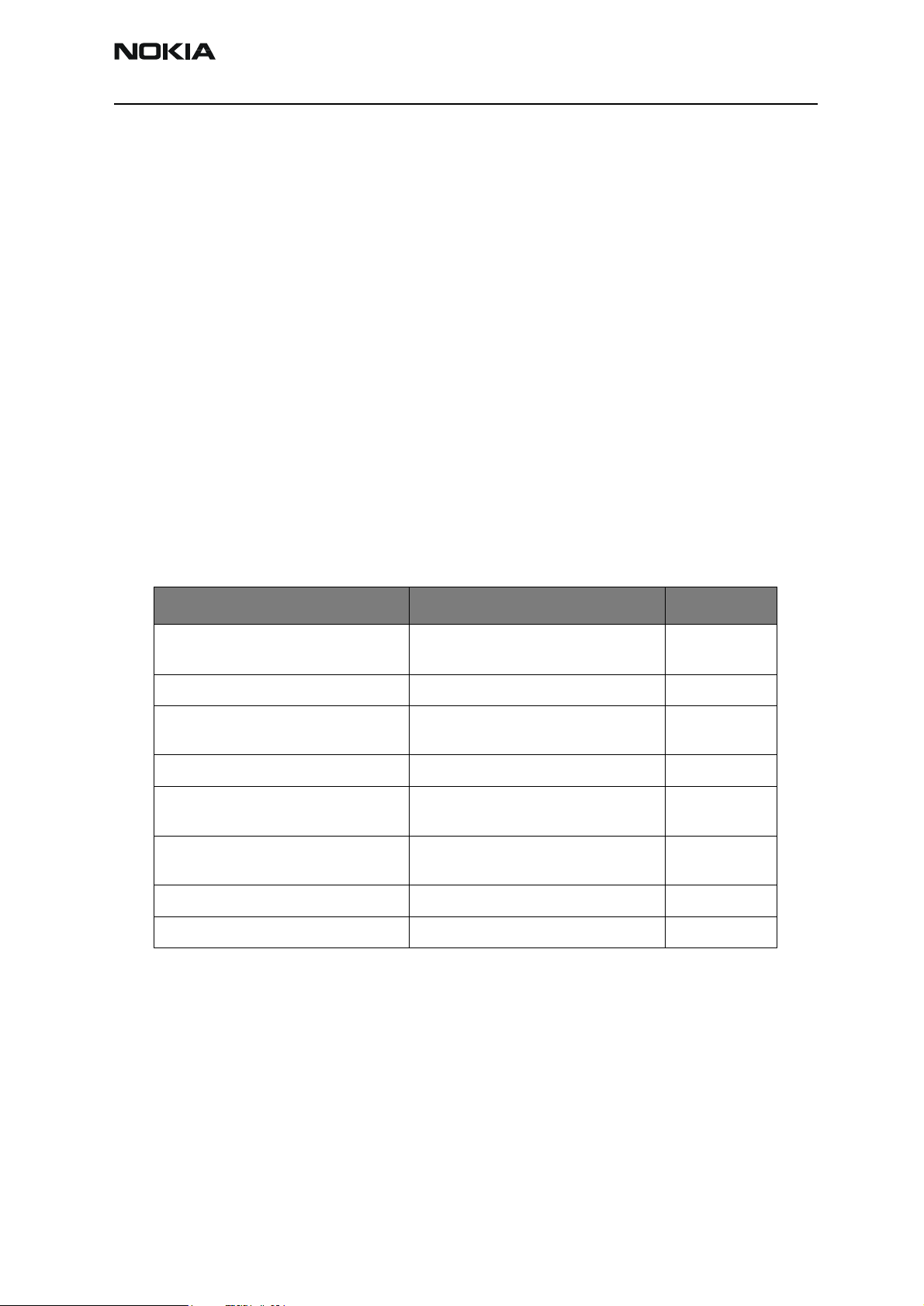
REGULATORS
UEM has 6 regulators for BB power supplies and 7 regulators for RF power supplies. VR1
regulator has 2 outputs VR1a and VR1b. In addition there are 2 current generators IPA1
and IPA2 for biasing purposes.
Bypass capacitor (1uF) is required for each regulator output to ensure stability.
Reference voltages for regulators require external 1uF capacitors. Vref25RF is reference
voltage for VR2 regulator, Vref25BB is reference voltage for VANA, VFLASH1, VFLASH2,
VR1 regulators, Vref278 is reference voltage for VR3, VR4, VR5, VR6, VR7 regulators,
VrefRF01 is reference voltage for VIO, VCORE, VSIM regulators and for RF.
Table 1: UEM Regulators
BB RF Current
VANA: 2.78Vtyp 80mAmax VR1a:4.75V 10mAmax
VR1b:4.75V
Vflash1: 2.78Vtyp 70mAmax IPA2: 0-5mA
Vflash2: 2.78Vtyp
40mAmax
VSim: 1.8/3.0V 25mAmax VR3:2.78V 20mA
VIO: 1.8Vtyp
150mAmax
Vcore: 1.0-1.8V
200mAmax
VR2:2.78V 100mAmax
VR4: 2.78V 50mAmax
VR5: 2.78V 50mAmax
VR6: 2.78V 50mAmax
VR7: 2.78V 45mAmax
IPA1: 0-5mA
VANA regulator supplies internal and external analog circuitry of BB. It is disabled in
sleep mode.
Vflash1 regulator supplies LCD, IR-module and digital parts of UEM and Safari_GTE asic.
It is enabled during startup and goes to low Iq-mode in sleep mode.
Vflash2 regulator supplies data cable (DLR-3). It's enabled/disenabled through writing
register and default is off.
VIO regulator supplies both external and internal logic circuitries. It is used by LCD, flash
and UPP. Regulator goes in low Iq-mode in sleep mode.
Issue 1 11/02 ãNokia Corporation Page 9
Page 10

RH-13
System Module CCS Technical Documentation
VCORE regulator supplies DSP and Core part of UPP. Voltage is programmable and startup default is 1.5V. Regulator goes to low Iq-mode in sleep mode.
VSIM regulator supplies SIM card. Voltage is programmable. Regulator goes in to low Iqmode in sleep mode.
VR1 regulator uses two LDOs and a charge pump. Charge pump requires one external 1uF
capacitor in Vpump pin and 220nF flying capacitor between pins CCP and CCN. VR1 regulator is used by Safari_GTE RF ASIC.
VR2 regulator is used to supply external RF parts, lower band up converter, TX power
detector module and Safari_GTE. In light load situations VR2 regulator can be set to low
Iq-mode.
VR3 regulator supplies VCTCXO and Safari_GTE in RF. It's enabled always when UEM is
active. When UEM is in sleep mode VR3 is disabled.
RF IF
VR4 regulator supplies RF parts having low noise requirements. In light load situations
VR4 regulator can be set to low Iq-mode.
VR5 regulator supplies lower band PA. In light load situations VR5 regulator can be set to
low Iq-mode.
VR6 regulator supplies higher band PA and TX amplifier. In light load situations VR6 regulator can be set to low Iq-mode.
VR7 regulator supplies UHF VCO and Safari_GTE. In light load situations VR7 regulator
can be set to low Iq-mode.
IPA1 and IPA2 are programmable current generators. 27kΩ/1%/100ppm external resistor
is used to improve the accuracy of output current. IPA1 is used by lower band PA and
IPA2 is used by higher band PA.
The interface between the baseband and the RF section is handled also by UEM. It provides A/D and D/A conversion of the in-phase and quadrature receive and transmit signal
paths and also A/D and D/A conversions of received and transmitted audio signals to and
from the UI section. The UEM supplies the analog AFC signal to RF section according to
the UPP DSP digital control.
Charging Control
The CHACON block of UEM ASIC controls charging. Needed functions for charging controls are pwm-controlled battery charging switch, charger-monitoring circuitry, battery
voltage monitoring circuitry and RTC supply circuitry for backup battery charging (Not
used in RH-13). In addition external components are needed for EMC protection of the
charger input to the baseband module.
Page 10 ãNokia Corporation Issue 1 11/02
Page 11

RH-13
CCS Technical Documentation System Module
DIGITAL IF
Data transmission between the UEM and the UPP is implemented using two serial connections, DBUS (programmable clock) for DSP and CBUS (1.0MHz GSM and 1.08MHz
TDMA) for MCU. UEM is a dual voltage circuit, the digital parts are running from 1.8V
and the analog parts are running from 2.78V.
AUDIO CODEC
The baseband supports two external microphone inputs and one external earphone output. The inputs can be taken from an internal microphone, a headset microphone or from
an external microphone signal source through headset connector. The output for the
internal earpiece is a dual ended type output, and the differential output is capable of
driving 4Vpp to earpiece with a 60 dB minimum signal to total distortion ratio. Input and
output signal source selection and gain control is performed inside the UEM Asic according to control messages from the UPP. A buzzer and an external vibra alert control signals are generated by the UEM with separate PWM outputs.
UI DRIVERS
UEM has dedicated single output drivers for buzzer, vibra, IR, display LEDs and keyboard
LEDs. These generate PWM square wave to devices.
IR interface
The IR interface is integrated to UEM and data transfer is done via TXD and RXD paths.
UEM supports data speeds up to 115.2kbit/s.
IR module integrates a sensitive receiver and a built-in power driver. IR module itself
supports speeds from 9.6kbit/s to 1.152Mbit/s. UEM supports speeds up to 115.2 kbit/s.
Vflash1 supplies IR module except transmit LED. Transmit LED is supplied from VBAT and
maximum current is limited by serial resistor. TXD and RXD lines are connected to UEM
and shutdown is controlled by UPP through level-shifter V350.
AD CONVERTERS
There is 11-channel analog to digital converter in UEM. Some channels of the AD converter aren't used in RH-13 (LS, KEYB1-2). The AD converters are calibrated in the production line
SIM
The SIM interface is the electrical interface between the Subscriber Identify Module Card
(SIM card) and mobile phone (via UEM device). The UEM device contains power up/down,
port gating, card detect, data receiving, ATR-counter, registers and level shifting buffers
logic for SIM.
Technical information
UEM package is 168-pin CSP package with 150 signal pins, 16 thermal pins and 2 kelvin
pins. Package size is 12mm x 12mm with max. thickness of 1.23mm. Solder ball diameter
is 0.4mm +-0.05mm and ball pitch is 0.8mm.
Issue 1 11/02 ãNokia Corporation Page 11
Page 12

RH-13
System Module CCS Technical Documentation
UPP
Introduction
RH-13 uses UPPv8M ASIC. The RAM size is 8M. The processor architecture consists of
both DSP and MCU processors.
Blocks
UPP is internally partitioned into two main parts:
The Processor and Memory System (i.e. Processor cores, Mega-cells, internal memories,
peripherals and external memory interface) is known as the Brain.
Brain consists of the blocks: the DSP Subsystem (DSPSS), the MCU Subsystem (MCUSS),
the emulation control EMUCtl, the program/data RAM PDRAM and the Brain Peripherals–subsystem (BrainPer).
The NMP custom cellular logic functions. This is known as the Body.
Body contains all interfaces and functions needed for interfacing other baseband and RF
parts. Body consists of following sub-blocks: MFI, SCU, CTSI, RxModem, AccIF, UIF, Coder,
GPRSCip, BodyIF, SIMIF, PUP and CDMA (Corona).
Technical information
UPP package is 13x13-matrix CSP package with 144 signal pins. Package size is 12mm x
12mm with max. thickness of 1.40mm. Solder ball diameter is 0.5mm +-0.05mm and ball
pitch is 0.8mm.
Flash memory
Introduction
RH-13 uses 64 Mbit flash as an external memory. VIO is used as a power supply for normal in-system operation. An accelerated program/erase operation can be obtained by
supplying Vpp of 12 volt to flash device. Memory architecture consists of eight sectors of
8kB and 63 sectors of 64kB each.
The device has two read modes: asynchronous and burst. Burst mode read is utilized in
RH-13 except the start-up when asynchronous read is used for a short time.
In burst mode UPP supplies only the initial address and subsequent addresses are generated inside flash by the rising edge of Clock (FLSCLK in UPP). After acknowledging the
initial address the flash starts to deliver a continuous sequential data word stream. Data
stream continues until the end of the memory or until the user loads in a new starting
address or stops the burst in advance.
Technical information
Flash package is a CSP package with 40 signal pins and 4/8 support balls. Package max.
size is (WxLxH) 10,6mm x 11,0mm x 1.2mm. Solder ball diameter is 0.3mm and ball pitch
Page 12 ãNokia Corporation Issue 1 11/02
Page 13
RH-13
CCS Technical Documentation System Module
is 0.5mm.
UIHW
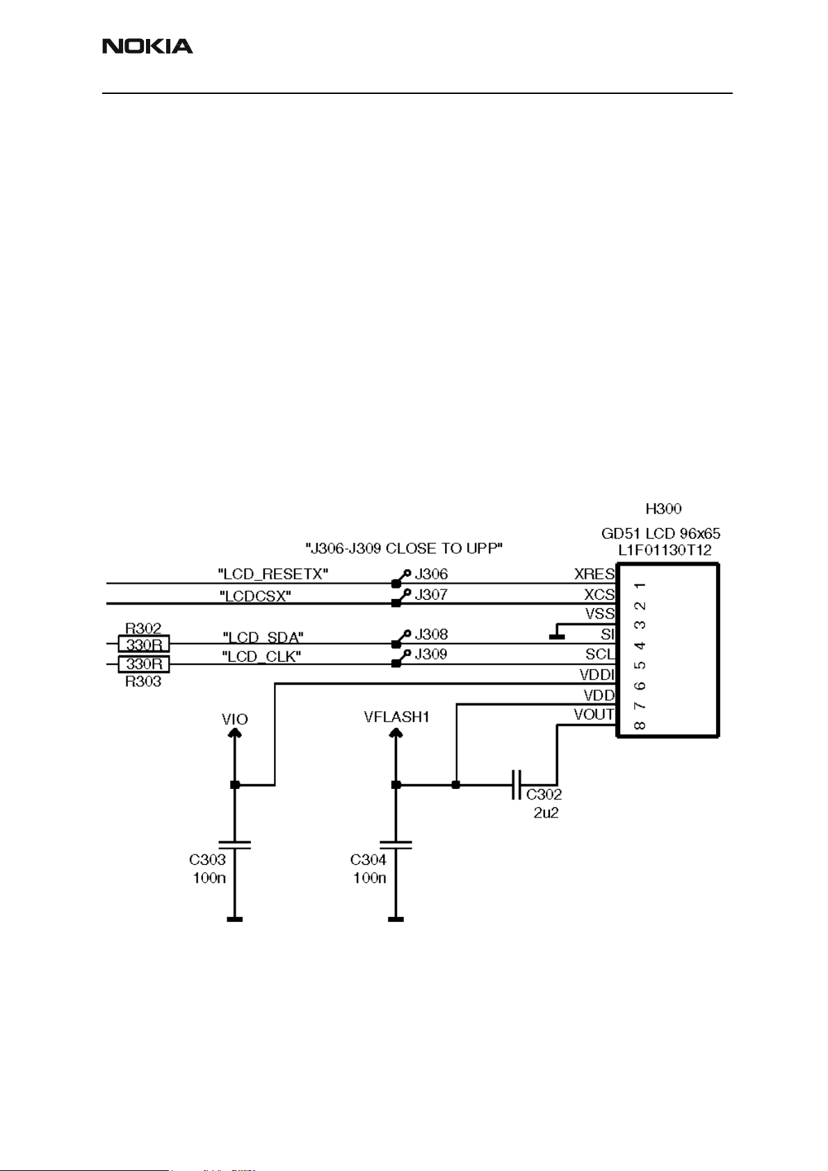
LCD
Introduction
RH-13 uses black/white GD51 96*65 full dot matrix display with COG driver. One vendor
- SEIKO SED15B0 - is used in RH-13.
Interface
LCD data, clock, chip select and reset signals come from the UPP. The VIO voltage is supplied to a logic voltage pin and the FLASH1 voltage is used to supply power to the LCD.
The LCD uses extra filtering capacitors to filter voltages. The booster capacitor (C302
2u2F) is connected between the booster pin and the Vflash1. The capacitor stores the
boosting voltage.
Figure 3: LCD interface
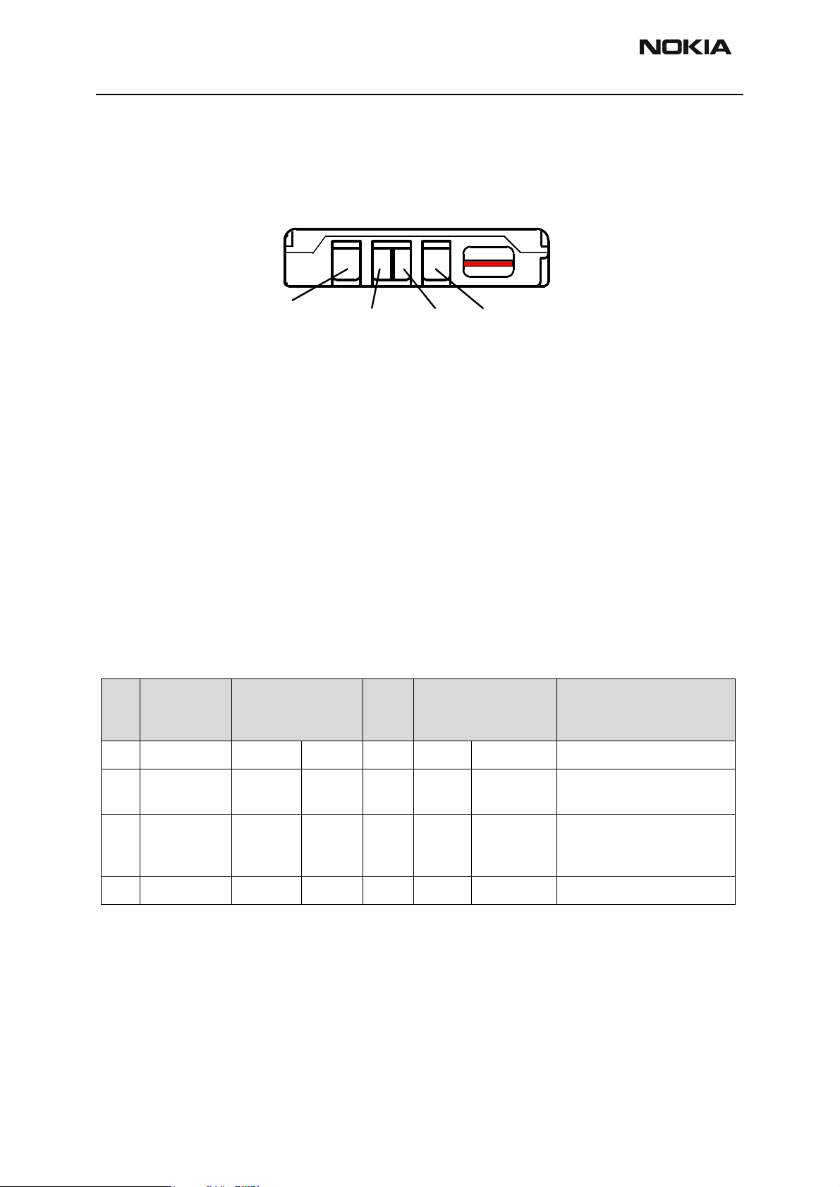
Keyboard
Introduction
All signals for the keyboard come from the UPP through the emifilter (Z300). The side
key, which does not go through the emifilter, and the power key signal are connected
directly to the UEM. The pressing of the power key is detected so that the switch power
Issue 1 11/02 ãNokia Corporation Page 13
Page 14
RH-13
123456789#0*Up
Down
End
Send
S Right
SLeft
System Module CCS Technical Documentation
key connects the PWONX of the UEM to the GND and creates an interruption. Side key
detection is achieved by connecting the line to the ground when pressing the side key
(volume up or down). The emifilter is the ESD and EMC protection.
The matrix-based keyboard interface consists of a scan column I/O data register and a
row of data register. In the keyboard scanning procedure, the MCU performs access to
these registers to find out which key was pressed. Scanning is an interrupt-based procedure, i.e. an interrupt generated when the key is pressed, and then the MCU can start the
scanning procedure. The side keys are also detected in the same way as the other keys,
except that there is no metaldome, and the middle pin is directly connected to the
ground.
Figure 4: Placement of keys
Power Key
All signals for keyboard come from UPP ASIC except PWRONX line for PWR key which is
connected directly to UEM. Pressing of PWR key grounds PWRONX line and UEM generates an interrupt to UPP which is then recognized as a PWR key press.
Keys
All signals for the keyboard come from the UPP through the emifilter (Z300) except the
side key, which will not go through the emifilter, and the power key signal, which is connected directly to the UEM. Pressing of the power key is detected so that the switch of
the power connects PWONX of the UEM to the GND and creates an interruption. Side key
detection is done by connecting line to ground when pressing the side key (volume up or
down). Emifilter is ESD and EMC protection.
The matrix-based keyboard interface consists of scan column I/O data register and of a
row data register. In keyboard scanning procedure, MCU performs access to these regis-
Page 14 ãNokia Corporation Issue 1 11/02
Page 15
RH-13
CCS Technical Documentation System Module
ters to find out which key was pressed. Scanning is an interrupt procedure, i.e., an interrupt is generated when key is pressed and then the MCU can start the scanning
procedure. Side keys are also detected in the same way as other keys except that there is
no metaldome, but the middle pin is directly connected to the ground.
Table 2: Matrix of key detection lines
S0 / P00 S1 / P01 S2 / P02 S3 / P03 S4 / P04
R0 / P10 Side key / Vol.
down
R1 / P11 Side key / Vol.
down
R2 / P12 Side key / Vol.
down
R3 / P13 Side key / Vol.
down
R4 / P14 Side key / Vol.
down
R5 / P15 Reserved Side key / Vol. upSide key / Vol. upSide key / Vol. upSide key / Vol.
NC Send End NC
Soft left Up Down Soft right
1 4 7 *
2 5 8 0
3 6 9 #
up
NC = Not Connected
Lights
Introduction
RH-13 has 12 LEDs for lighting purposes. 6 of them (V300-V303, V310-V311) are for display and 6 (V304-V309) for keyboard. LEDs are green light -emitting and SMD throughboard-firing.
Interfaces
Display lights are controlled by Dlight signal from UEM. Dlight output is PWM signal
which is used to control average current going through LEDs. When battery voltage
changes new PWM value is written to the PWM register. This way brightness of the lights
remains the same with all battery voltages within range. Frequency of the signal is fixed
128Hz.
Keyboard lights are controlled by Klight signal from the UEM. Klight output is also PWM
signal and is used similar way as Dlight.
Technical information
Each LED requires hole in PWB where the body of LED locates in hole and terminals are
soldered on component side of module PWB. LEDs have white plastic body around the
diode itself which directs the emitted light better to UI-side. Current for LCD lights is
limited by resistor between Vbatt and LEDs. For keyboard lights there are resistors in par-
Issue 1 11/02 ãNokia Corporation Page 15
Page 16
RH-13
System Module CCS Technical Documentation
allel.
Vibra
Introduction
Vibra is located to D-cover and is connected by spring connectors on the left bottom side
of the engine. Vibra manufacturers for RH-13 are Namiki and Matsushita.
Interfaces
Vibra is controlled by PWM signal VIBRA from UEM. With this signal it is possible to control both frequency and pulse width of signal. Pulse width is used to control current
when battery voltage changes. With frequency control it is possible to search optimum
frequency to have silent and efficient vibrating.
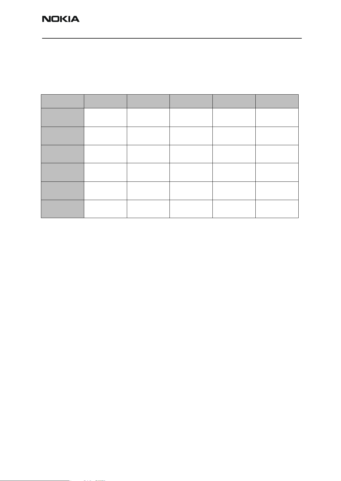
Table 3: Electrical parameters
Parameter Requirement Unit
Rated DC Voltage 1.3 V
Rated speed 9500 ±3000 rpm
Rated current 115 ±20 mA
Starting current 150 ±20 mA
Armature resistant 8.6 ohm
Rated DC voltage being able to use 1.2 to 1.7 V
Starting DC voltage min. 1.2 V
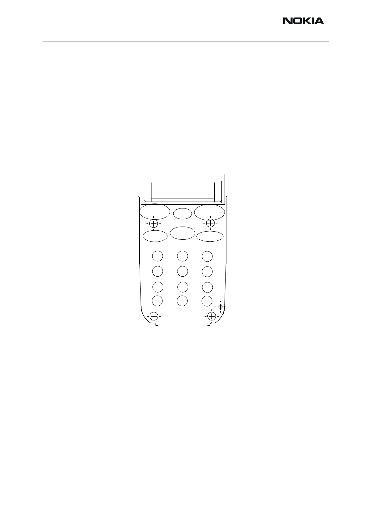
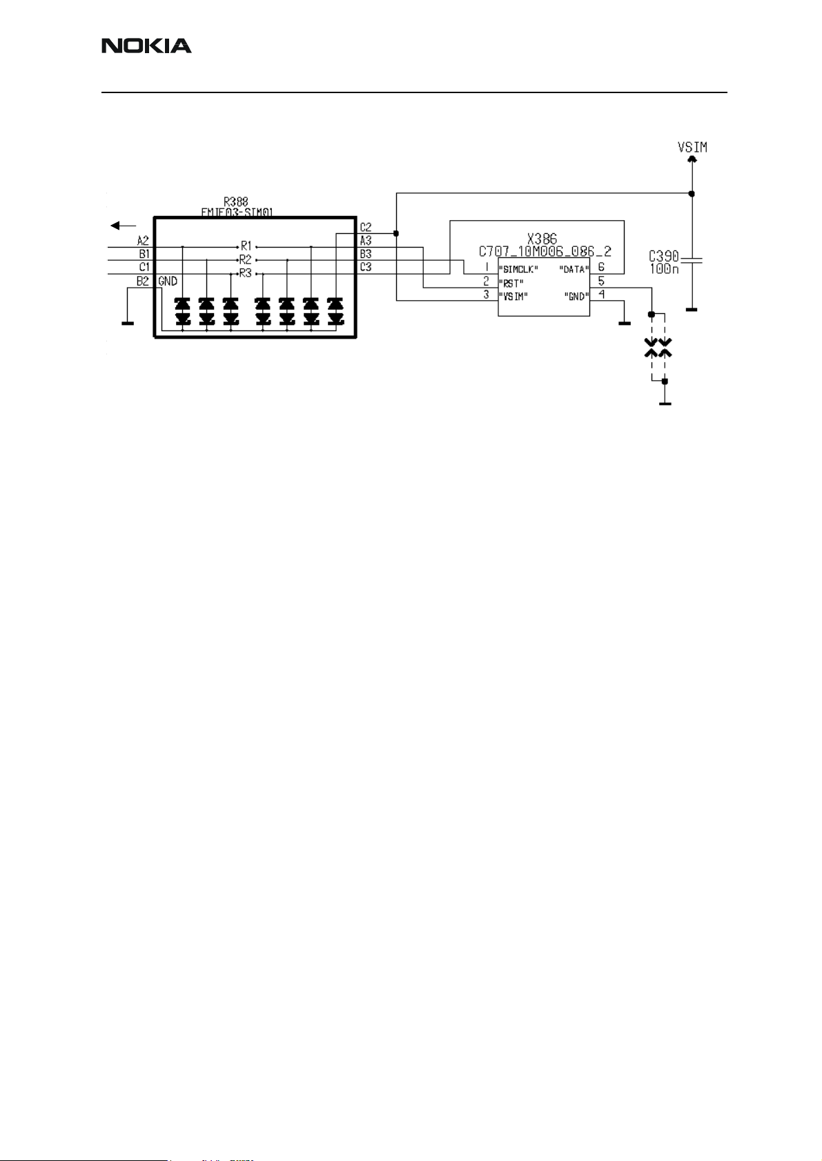
SIM card reader
Introduction
RH-13 is supporting SIM card reader. The SIM is located in the bottom of the engine. The
SIM card reader is manufactured by Amphenol.
Interface
The SIM card reader is connected by spring connectors on the PWB. EMC/ESD protection
is done by ASIP, R388. It is a CSP component. VSIM provides power supply voltage to the
SIM card reader. Two spark gaps are put to the no connected pin to provide protection
from ESD.
Page 16 ãNokia Corporation Issue 1 11/02
Page 17
RH-13
CCS Technical Documentation System Module
Figure 5: SIM block
UEM
Technical information
The SIM interface is split between UEM and UPP. This has been done in order to reduce
the amount of interconnections on the SIM interface between the UPP and the UEM. The
SIM interface control logic and UART is integrated into the UPP. The SIM interface startup and power down sequence, including timing and reset generation is implemented in
UEM. The SIM interface in the UPP supports the SIM speed enhancement features, which
improves the data transfer rate in the SIM interface.
The UEM contains the SIM interface logic level shifting. UPP SIM interface logic levels
are 1.8V. The SIM interface can be programmed to support 3V and 1.8V SIMs. A 5V SIM
interface is not supported. The SIM supply voltage is selected by a register in the UEM. It
is only allowed to change the SIM supply voltage when the SIM IF is powered down. The
SIM power up/down sequence is generated in the UEM. This means that the UEM generates the RST signal to the SIM.
The data communication between the card and the phone is asynchronous half duplex.
The clock supplied to the card is in GSM system max. 3.25 MHz and TDMA 4.68Mhz. The
data baudrate is SIM card clock frequency divided by 372 (by default), 64, 32 or 16. The
protocol type, that is supported, is T=0 (asynchronous half-duplex character transmission
as defined in ISO 7816-3).
Audio HW
Earpiece
Introduction
RH-13 earpiece is located on the top of the engine.
The speaker is a dynamical one. It is very sensitive and capable of producing relatively
high sound pressure also at low frequencies. The speaker capsule and the mechanics
around it together make the earpiece.
Issue 1 11/02 ãNokia Corporation Page 17
Page 18

RH-13
System Module CCS Technical Documentation
Interface
The earpiece is driven directly by UEM (EARP and EARN). Both lines are ESD protected
inside UEM (±8kV). The earpiece is connected on the PWB by spring connectors.
Technical information
The rated impedance of the earpiece is 32Ω and sensitivity at 1mW/1kHz is 103±3dB.
The diameter of the earpiece is 13.2mm and the thickness is 2.7mm. For more detailed
specification see data sheets under material code 5140067.
Microphone
Introduction
The microphone is an electret microphone with omnidirectional polar pattern. It consists
of an electrically polarized membrane and an metal electrode which form a capacitor. Air
pressure changes(i.e. sound) moves the membrane which causes voltage changes across
the capacitor. Because the capacitance is typically 2 pF a FET buffer is needed inside the
microphone capsule for the signal generated by the capacitor. Because of the FET the
microphone needs a bias voltage.
Buzzer
The microphone manufacturer for RH-13 is Matsushita.
Interface
The microphone input is driven single-ended from UEM MIC1P. The microphone bias
voltage is generated by MICB1. Esd protection is implemented by spark cap, buried
capacitor (Z153) and a special microphone capsule.
Technical information
Output impedance is 2,2kΩ and sensitivity at 1Pa/1kHz is -42±3dB. The diameter of the
microphone is 6.0mm and the thickness is 2.7mm. For more detailed specification see
data sheets under material code 5140213.
Introduction
The operating principle of buzzer is magnetic. The diaphragm of the buzzer is made of
magnetic material and it is located in a magnetic field created by a permanent magnet.
The winding is not attached to the diaphragm as is the case with the speaker.The winding is located in the magnetic circuit so that it can alter the magnetic field of the permanent magnet thus changing the magnetic force affecting the diaphragm. Buzzer's useful
frequency range is approximately from 2 kHz to 5kHz.
Interface
The buzzer is connected between Vbat and UEM. The UEM's buzzer driver generates
Page 18 ãNokia Corporation Issue 1 11/02
Page 19
RH-13
Battery
CCS Technical Documentation System Module
PWM signal which controls the frequency and pulse width of signal of the buzzer. The
buzzer has spring contacts to PWB.
Technical information
Rated input voltage is 3.6V and resonance frequency is 2700Hz. The size of the buzzer is
11mm x 10.2mm x 2.2mm without a gasket. For more detailed specification see data
sheets under material code 5140229.
Battery
Phone battery
Introduction
Li-Ion 1000mAh battery BLB-3 is used in RH-13 by default. There is also possible use
BLB-2 (Li-Ion 750mAh) battery. Its thickness and capacity is smaller. Even though its
thickness is smaller it fits electrically and mechanically in RH-13.
Interface
The battery block contains NTC and BSI resistors for temperature measurement and battery identification. The BSI fixed resistor value indicates the chemistry and default
capacity of a battery. NTC-resistor measures the battery temperature. Temperature &
capacity information is needed for charge control. These resistors are connected to BSI
and BTEMP pins of battery connector. Phone has pull-up resistors (R202 and R203) for
these lines so that they can be read by A/D inputs in the phone. Dual resistor R205 is esd
protection. These can be left out if the protection of UEM itself is enough. There are also
spark caps in the battery lines to prevent esd. There is also EMI-filter between VBAT and
battery connector for EMC. See schematic.
Figure 6: Battery connection diagram
UEM
C220
1n
R203
100k
R205/1
10R
VFLASH1VANA VBAT
R202
100k
C108
10p
connector
VBATT
BSI
BTEMP
OVERCHARGE/
OVERDISCHARGE
PROTECTION
Li-Io n
C217
1n
R205/2
10R
C109
10p
GND
Batteries have a specific red line which indicates if the battery has been subjected to
excess humidity. The batteries are delivered in a protection mode, which gives longer
Issue 1 11/02 ãNokia Corporation Page 19
Page 20
RH-13
1(+)
2(BSI)
3(BTEMP)
4(GND)
System Module CCS Technical Documentation
storage time. The voltage seen in the outer terminals is zero (or floating), and the battery
is activated by connecting the charger. Battery has internal protection for overvoltage
and overcurrent.
Figure 7: BLB-3 Battery contacts (BLB-2 has the same interface)
Technical information
Local mode is entered by inserting 560 Ohm resistors to these lines. In production following 1% resistors are needed in the case of BLB-3:
Normal/Calibration mode: BSI = 75k, BTEMP = 47k
Local mode: BSI = 560, BTEMP = 560
Test mode: BSI = 3.3k BTEMP = 560
Battery connector
RH-13 uses SMD type battery connector. This makes phone easier to assemble in production and connection between battery and PWB is more reliable. Battery connector is
manufactured by Hirose.
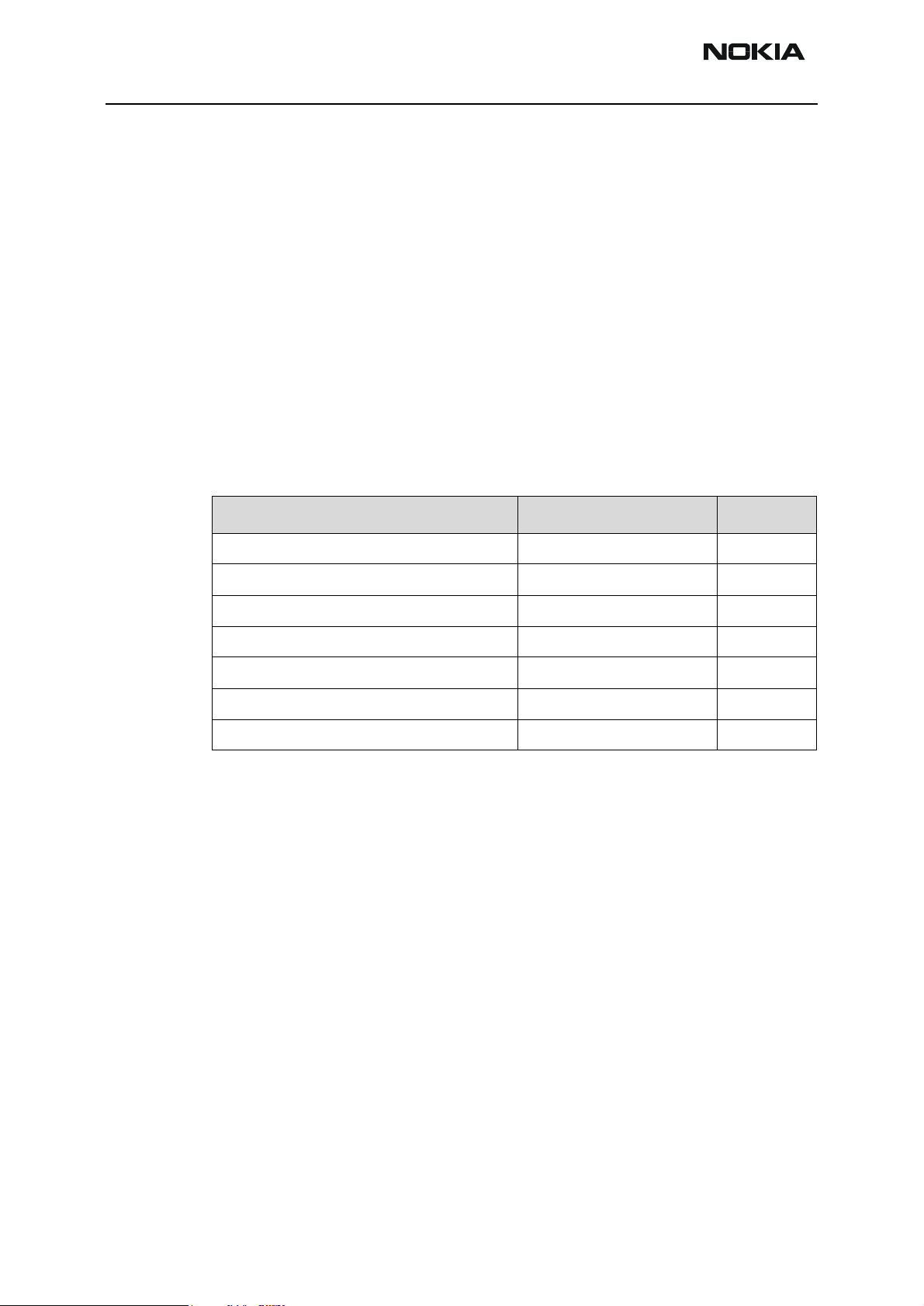
Table 4: Battery connector interface
# Signal name Connected from - to Batt
I/O
1 VBAT (+) (batt.) VBAT I/O Vbat 3.0-5.1V Battery voltage
2 BSI BSI
(batt.)
3 BTEMP BTEMP
(batt.)
4 GND GND GND Gnd Ground
UEM Out Ana. Battery size indicator
UEM Out Ana. 40mA /
Signal properties
A/--levels--freq./
timing
Switch
400mA
Description / Notes
Battery temperature indicator
Accessories Interface
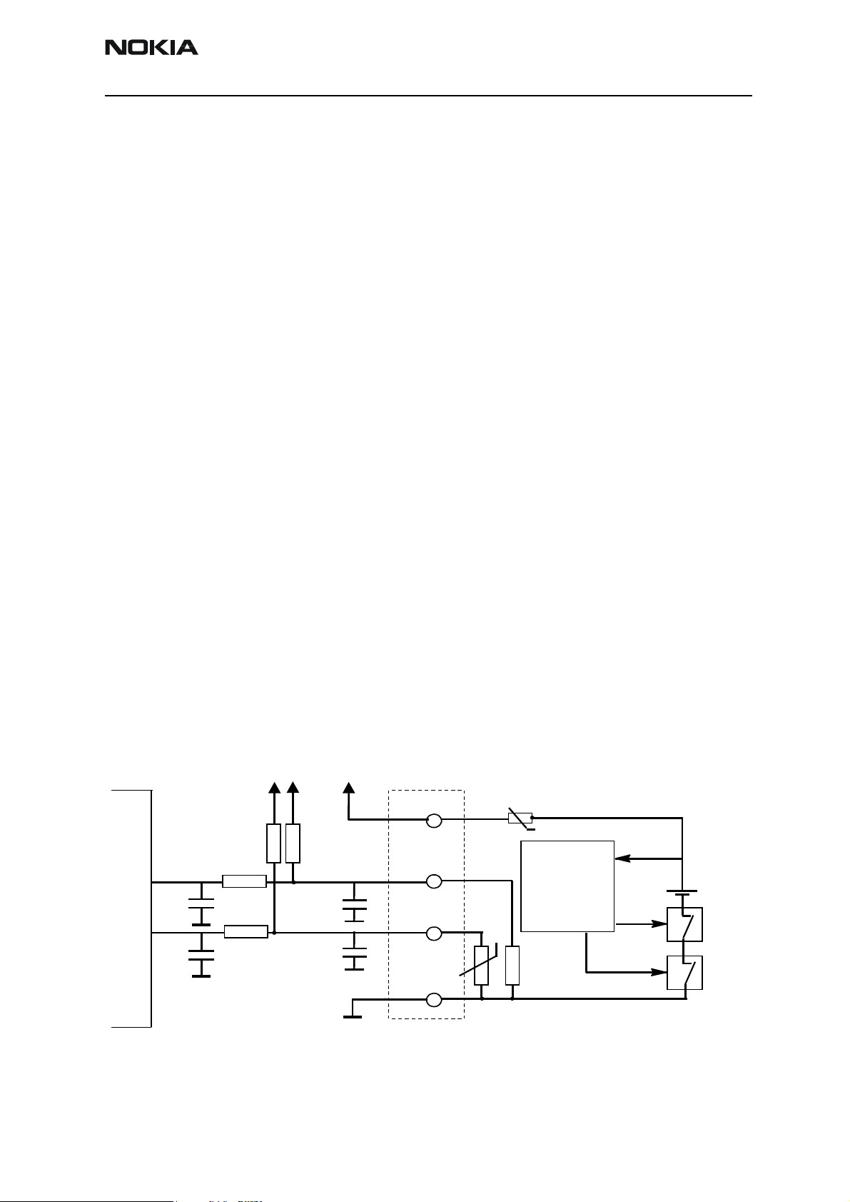
System connector
Introduction
RH-13 uses same accessories as Nokia 61XX and 51XX products via similar system connector. RH-13 supports headsets HDC-9P, HDE-1P and loopset LPS-1P.
Page 20 ãNokia Corporation Issue 1 11/02
Page 21

RH-13
CCS Technical Documentation System Module
Interface
Interface is compatible with Nokia 61XX and 51XX products. An accessory is detected by
the HeadInt and HookInt line which are connected to system connector. The HookInt line
is used to activate or end a call (only in HDC-9P).
Figure 8: System connector
1 VCHARIN1,2,K
2GND
3 VCHARIN1,2,K
4PWMO
5PWMO
Technical information
Esd protection is made by spark caps, buried capacitor (Z154 - Z155 and Z157) and
inside UEM which is protected ±8kV. RF and BB noises are prevented by inductors.
IR module
Introduction
6MICP
7MICN
8XMIC
9SGND
10 XEAR
11 MBUS
12 FBUSRXO
13 FBUSTXO
14 GND
X100
IR module is used to short-range data transfer. It is a low-power infrared transceiver
module complaint to the IrDA 1.2 standard for fast infrared data communication. RH-13
is using Vishay's TFDU5102 or TFDU5103 IR module (in the following figure, TFDU5102 is
used). The IR module is located to the top of the engine side next to Power Up button.
Issue 1 11/02 ãNokia Corporation Page 21
Page 22

RH-13
System Module CCS Technical Documentation
Interface
The transmit of the IR module goes as follow. Transmit is controlled by TXD line which
comes from UPP. Between UPP and IR module there is UEM which makes lever-shifter
from 1.8V to 2.78V. VBAT gives power supply to transmit led and serial resistor (R350)
limits current. There is also filter capacitor (C351) on VBAT-line to give proper voltage.
Receiving infrared data to IR led, it goes straight to UEM by RXD line.
VFLASH1 is the power supply of the IR module, except for transmission. That is also filtered by capacitor C350. The IR module has one-control pin to control shut down. Component V350 is control-lever-shifter which is used to change proper voltage to IR
module from UPP (GENIO(10) for shutdown.
Figure 9: IR interface
UEM
Technical information
The IR interface is designed into the UEM. The IR link supports speeds from 9600 bit/s to
1.152 MBit/s, up to 1m. A special baud rate is used for the NMP specific speech and control information transmission. This dedicated protocol has special HW support for
extracting the audio and control information from each other.
Page 22 ãNokia Corporation Issue 1 11/02
Page 23

RH-13
CCS Technical Documentation System Module
Charger IF
Introduction
The charger connection is implemented through the system connector. The system connector supports charging with both plug chargers and desktop stand chargers. The
charger is 2-wire or 3-wire galvanic charger. Connecting a charger creates voltage on
VCHAR input of the UEM. When VCHAR input voltage level is detected to rise above
VCHDET+ threshold by CHACON charging starts. VCHARDET signal is generated to indicate the presence of the charger.
The charging voltage and current are measured to identify the charger and controlling
charging. In the case of 3-wire charger PWM-control signal is used to control charger
voltage. The pulse duty cycle of the PWM can vary from 0%…100% which is the normal
operating range.
Interface
The fuse F100 protects phone from too high currents for example when broken or pirate
chargers are used. L100 protects engine from RF noises, which may occur in charging
cable. V100 protects UEM asic from reverse polarity charging voltage and from too high
charging voltage. C105 is also used for ESD and EMC protection. Charger control line
(PWM) uses spark gaps and T-filter (dual R107 10k and C107 10n).
Data cable
Introduction
The data cable is used to transfer data between the phone and a PC or a service box. RH13 uses DAU-9P/S and DLR-3P/S data cables. The data cables are a RS232 compatible.
DLR-3 needs also power supply to logic and processor device inside the cable. This is supplied from the phone.
Interface
System connector is used to transfer data to/from PC. Vflash2 voltage is supplied power
to DLR-3 data cable through dual mosfet transistor V151. As Vflash2 shutdown is too
slow, Genio(0) is also used for controlling the mosfet. Genio(2) is also used to control RST
command because hookint-line is too slow to poll RST command.
Test interfaces
Production test pattern
Interface for RH-13 production testing is 5pin pad layout in BB area. Production tester
connects to these pads by using spring connectors. Interface includes MBUS, FBUSRX,
FBUSTX, VPP and GND signals. Pad size is 1.7mm. Same pads are used also for AS test
equipment like module jig and service cable.
Issue 1 11/02 ãNokia Corporation Page 23
Page 24

RH-13
X
D
System Module CCS Technical Documentation
Figure 10: Top view of production test pattern
Other test points
Because BB ASICs and Flash memory are CSP components the visibility to BB signals is
very poor. This makes measuring of most of the BB signals impossible. In order to debug
BB at least in some level the most important signals can be accessed from 0.6mm test
points.
7.
MBUS
3.
FBUS_R X
8.
GND
2.
FBUS_TX
6.
VPP
Figure 11: Telescoping pattern between UPP and UEM
UEM (D200)
BUSDA
J414
J413
SLEEPX
J403
J402
PURXDBUSCLK
SLEEPCLK
J404
J405
UEMINT
CBUSDA
J407
J415
DBUSEN1X
CBUSENX
J408
J412
FBUSRX
CBUSCLK
J406
J409
MBUSTX MBUSR
FBUSTX
J411
J410
UPP (D400)
EMC
General
EMC protection has been designed in BB so that signals from system connector have
passive filtering components for EMI/ESD protection. ESD protection for these signals is
built inside UEM. Signals have protection inside UEM which can handle 8kV ESD pulses.
Page 24 ãNokia Corporation Issue 1 11/02
Page 25

RH-13
CCS Technical Documentation System Module
BB component and control/IO line protection
Keyboard lines
ESD protection for keyboard signals is implemented by using Emifilter Z300 detection
The distance from the A-cover to the PWB is made longer with the spikes in the keymat.
PWB
All edges are grounded from both sides of PWB and solder mask is opened from these
areas. Target is that any ESD pulse faces ground area when entering the phone, for
example between mechanics covers.
All holes in PWB are grounded and plated through holes. Except LED holes, which can
not be grounded.
LCD
ESD protection for LCD is implemented by connecting metal frame of LCD in to ground.
Two clips are used to connect the LCD module to the engine, and those two clips are also
used to make the metal frame ground connection. Software also takes care of the LCD's
crashing in case of ESD pulse.
Microphone
Microphone's metal cover is connected to ground and there are spark gaps on PWB.
Microphone is unsymmetrical circuit, which makes it well protected against EMC.
Earpiece, buzzer and IRDA
These RH-13 components are protected by mechanics, this is possible because RH-13
does not have a changeable A-cover.
Bottom connector lines
Table 5: Bottom connector signals with EMC protections
Bottom connector signals that have EMC protection
protection
type
VIN CHRG_
CTRL
MICP XMIC SGND XEAR MBUS FBUS_R
X/TX
ferrite bead
(600_/
100MHz)
ferrite bead
(42_/
100MHz)
spark gaps x x x x x x x
PWB capacitors
x
x x x x
x x x x
Issue 1 11/02 ãNokia Corporation Page 25
Page 26

RH-13
System Module CCS Technical Documentation
RC-circuit x x x x
capacitor to
ground
T- filter x x x
x x x x x
Battery connector lines
BSI and BTEMP lines are protected with spark gaps, caps (10p) and RC-circuit (10k & 1n)
where resistors are size 0603.
MBUS and FBUS
Opening in the protective metal deck underneath the battery is so small that ESD does
not get into MBUS and FBUS lines in the production test pattern.
Page 26 ãNokia Corporation Issue 1 11/02
Page 27

RH-13
Accessories
VIBRA
2
3
4
7
8
CCS Technical Documentation System Module
Transceiver interfaces
Figure 12: Transceiver block naming for interfaces
TRANSC EIVER
LCD DRIVER
B&W
display
BACKLIG HT
USER INTERFACE
BACKLIG HT
✉
1
☎
5
0#
6
9
EARPIECE
ANT
EXT
RF
Ostrich
JTAG
Prod.TEST I/F
RF
ENGINE
BB
IN F R A R ED
AUDIO
(disc r)
BUZZER
BSI
BTemp
MIC
Ext. Audio
BATTER Y
CHARGER
Module
BB - RF Interface Connections
All the signal descriptions and properties in the following tables are valid only for active
signals so the signals are not necessarily present all the time.
Issue 1 11/02 ãNokia Corporation Page 27
Page 28

RH-13
System Module CCS Technical Documentation
Table 6: BB - RF Interface Signal Description
Signal
Ri
Name
p
#
DAMPS,
GSM19
00
Connected
from--- to
BB
I/O
RFICCNTRL(2:0) RF IC Control Bus from UPP to RF IC (SAFARI_GTE)
Signal Properties
A/D--Levels---Freq./
Timing resolution
Description / Notes
0 RFBUS-
CLK
UPP RFIC In Dig 0/1.8V
(0:
<0.4V
1: >1.4
9.72 MHz
TDMA/
13MHz
GSM
RF Control serial bus bit clock
V)
1 RFBUSDAUPP/
RFIC
2 RFBUSE
UPP RFIC In Dig RFIC Chip Sel X
RFIC
UPP
I/O Dig Bi-directional RF Control serial
bus data,
N1X
PUSL(2:0) Power Up Reset from UEM to RF IC (SAFARI_GTE)
0 PURX UEM RFIC Out Dig 0/1.8V 10us Power Up Reset for RF IC
1 SLEEPX UPP RFIC Out Dig 0/1.8V System clock EN, power safe
function
GENIO(28:0) General I/O Bus connected to RF, see also separate collective GENIO(28:0)
table. Control lines from UPP GENIOs to RF
8 TX_ENA
UPP RF Out Dig 0/1.8V Tx power enable
BLE
9 TX_GAI
UPP RF Out Dig 0/1.8V Tx gain control
N_CRTL
11 BAND-
UPP RF Out Dig 0/1.8V Lo/Hi band selection
SEL
RFCLK (not BUS -> no rip #) System Clock From RF To BB, original source VCTCXO, buffered (and fre-
quency shifted, RH-13 only) in RF IC (SAFARI_GTE)
RFCLK VCTCX
O ->
RFIC
RFClk
RF UPP In Ana0 System Clock slicer Ref GND, not
GND
UPP In An
a
800mVpp
typ (FET
probed)
Bias DC
blocked
at UPP
input
19.2 MHz
(VCTCXO)
RFClk to BB
19.44MHz
TDMA/
13MHz GSM
System Clk from RF to BB
separated from PWB GND layer
SLOWAD(6:0) Slow Speed ADC Lines from RF block
5 RXTEMP
RF
Power
detection
module
UEM In Ana0/2.7V
dig
- Rx bandfilterTemperature signal
to UEM, NTC resistor (47k)
Page 28 ãNokia Corporation Issue 1 11/02
Page 29

RH-13
CCS Technical Documentation System Module
6 PATEMP
RFCONV(9:0) RF- BB differential Analog Signals: Tx I&Q, Rx I&Q and reference voltage
0 RXIP RFIC UEM In An
RF
Power
detection
module
UEM In Ana0.1-2.7V - Tx PA Temperature signal to UEM,
NTC in Power Detection Module
1.4Vpp
max. diff.
a
0.5Vpp
typ
bias
1.30V
Differential positive/negative inphase Rx Signal
1 RXIN
2 RXQP Diff. Positive/negative quadrature
phase Rx Signal
3 RXQN
4 TXIP UEM RFIC Out An
2.2Vpp
max. diff.
a
0.6VppTy
p
Bias
1.30V
Differential positive/negative inphase Tx Signal
5 TXIN
6 TXQP Differential positive/negative
quadrature phase Tx Signal
7 TXQN
9 VREFRFO1UEM RFIC Out Vref1.35 V RF IC Reference voltage from
UEM
RFAUXCONV(2:0) RF_BB Analog Control Signals to/from UEM
1 TXP-
WRDET
TXP
Det.
UEM In Ana0.1-2.4 V50 us Tx PWR Detector Signal to UEM
Module
2 AFC UEM VCTCXOOut Ana0.1-2.4
V
VRF Globals instead of Bus
Regulated RF SupplyVoltages from UEM to RF.Current values are of
the regulator specifications, not the measured values of RF
VR1 A UEM RFIC Out Vreg4.75 V
+- 3%
10 mA
max.
Automatic Frequency Control for
VCTCXO
UEM, charge pump + linear regulator output. Supply for UHF
synth phase det ….
VR1 B UEM RFIC Out Vreg4.75 V
+- 3%
10 mA
max.
UEM, charge pump + linear regulator output. Supply for Tx VHF
VCO
Issue 1 11/02 ãNokia Corporation Page 29
Page 30

RH-13
System Module CCS Technical Documentation
VR2 UEM RFDis
cr./
RFIC
VR3 UEM VCTCXOOut Vreg2.78 V
VR4 UEM RFIC Out Vreg --”-- 50 mA
VR5 UEM RFIC Out Vreg --”-- 50 mA
VR6 UEM RFIC Out Vreg --”-- 50 mA
VR7 UEM RFIC,
UHF
VCO
IPA1 UEM RF PA Out Iout0-5 mA Settable Bias current for RF PA L-
IPA2 UEM RFPA Out Iout0-5 mA Settable Bias current for RF PA
Out Vreg 2.78 V
+- 3%
+- 3%
Out Vreg--”-- 45mA UEM linear regulator. Power sup-
100 mA
max.
20 mA
max.
max.
max.
max.
UEM linear regulator. Supply voltage for
Tx IQ filter and IQ to Tx IF mixer.
UEM linear regulator. Supply for
VCTCXO + RFCLK Buffer in RF IC.
UEM linear regulator. Power Supply for LNA / RFIC Rx chain.
UEM linear regulator. Power Supply for RF low band PA driver section.
UEM linear regulator. Power supply for RF high band PA driver
section.
ply for RF Synths
Band
H-band
VFLASH1UEM RFIC Out Iout2.78V ~2mA UEM linear regulator common for
BB. RFIC digital parts and RF to
BB digi IF.
VR1 A UEM RFIC Out Vreg4.75 V
VBATT, Global
VBATTRF
Batt
Conn
RFPA Out Vb
+- 3%
3…5V 0…1A
att
10 mA
max.
2A peak
UEM, charge pump + linear regulator output. Supply for UHF
synth phase det ….
Raw Vbatt for RF PA
BB Internal connections
UEM Block Signal Description
Table 7: UEM Block SIgnals to UPP
Signal
Ri
Name
p
DAMPS/
GSM19
#
00
RFCONVDA(5:0)*
Connected
from -- to
UEM
I/O
1.8V digital interface between UPP and UEM. RF Converter CLK, Rx and
Tx I&Q data (bit stream signals).
Signal Properties
A/D--Levels---Freq./
Timing resolution
Description / Notes
0 RFCON-
VCLK
UPP UEM In Dig0/1.8 V RF Converter Clock
Page 30 ãNokia Corporation Issue 1 11/02
Page 31

RH-13
CCS Technical Documentation System Module
1 RXID UEM UPP O
(PDM) RxI Data
ut
2 RXQD (PDM) RxQ Data
3 TXID UPP UEM In (PDM) TxI Data
4 TXQD (PDM) TxQ Data
5 AUXDA UPP UEM In Auxiliary DAC Data
RFCONVCTRL(2:0)* 1.8V digital interface between UPP (DSP) and UEM, RF Converter and
UEM RF IF bi-directional serial Control Bus, "DBUS",
0 DBUS-
CLK
UPP UEM In Dig0/1.8 V 9.72MHz
TDMA/
Clock for Fast Control to UEM
13MHz
GSM
1 DBUSDA In
Fast Control Data to/from UEM
/
O
u
2 DBUSEN
In Fast Control Data Load /Enable to UEM
X
AUDUEMCTRL(3:0)* 1.8V digital interface between UPP (MCU) and UEM, Bi-directional Control
Bus "CBUS"
0 UEMINT UEM UPP
1 CBUS-
UPP UEM
CLK
2 CBUSDA
3 CBUSEN
O
Dig0/1.8 V UEM Interrupt
ut
In 1.08 MHz
TDMA/
1.00MHz
GSM
In/
O
u
In
Clock for Control/Audio Converters in
UEM
Control Data
Control Data Load Signal
X
AUDIODATA(1:0)* 1.8V digital audio interface between UPP and UEM audio codec, PDM data
clocked by CBUSCLK
0 EARDATAUPP UEM In Dig0/1.8 V PDM Data for Downlink Audio, clocked
by CBUSCLK
1 MIC-
DATA
UEM UPP O
ut
PDM Data for uplink Audio, clocked by
CBUSCLK
ISIMIF(2:0)* 1.8V digital SIM signals between UPP and UEM, wired, not used
0 SIMIO-
DAI
UPP UEM In
Dig0/1.8 V Data to/from SIM
/
O
u
Issue 1 11/02 ãNokia Corporation Page 31
Page 32

RH-13
System Module CCS Technical Documentation
1 SIMCLKI In Max.
3.25MHZ
GSM / max.
4.86MHz
TDMA
2 SIMIOC-
TRL
PUSL(2:0)* Power-Up & Sleep Control lines
0 PURX UEM UPP
RFICOutDig
1 SLEEPX UPP UEM In Power Save Functions, 0 at sleep
2 SLEEP-
CLK
IACCDIF(5:0)* BB Internal 1.8V Digital Accessory Buses between UPP and 2.7V level shifter
0 IRTX UPP UEM OutDig0/1.8 V 1.152
1 IRRX UEM UPP In Infrared Receive
2 MBUSTX UPP UEM In Dig0/1.8 V 9k6 b/s MBUS Transmit
UEM UPP O
In Control for SIM Interface
0/1.8 V Power Up Reset, 0 at reset
32 kHz 32 kHz Sleep Clock
ut
UEM
Mbit/s max
Clock to SIM
Infrared Transmit
3 MBUSRX UEM UPP O
ut
4 FBUSTXI UPP UEM In Dig0/1.8 V <115kb/s
5 FBUSRXI UEM UPP O
ut
Table 8: UEM Block Signals to BB & RF
Signal
Ri
Name
p
DAMPS/
GSM19
#
00
SLOWAD(6:0)* Slow Speed ADC Lines, UEM external
0 BSI BAT-
1 BTEMP Battery Temperature
5 RXTEMP RF/
Connected
from -- to
UEM In Ana 0 -2.7V Battery Size Indicator/FDL init
TERY
UEM In Ana 0 -2.7V Rx band filter Temperature, MeasNTC
resistor
UEM
I/O
Signal Properties
A/D--Levels--Freq./
Timing resolution
9k6 b/s
<7Mb/s
<1Mb/s
<115kb/s
<7Mb/s
MBUS Receive / FDL Clk
FBUS Transmit / FDL Tx
FBUS Receive / FDL Rx
Description / Notes
ured from NTC resistor
Page 32 ãNokia Corporation Issue 1 11/02
Page 33

RH-13
CCS Technical Documentation System Module
6 PATEMP RF;
PDMo
d
NTC
RFCONV(9:0)* RF- BB Analog Signals: Tx I&Q, Rx I&Q and ref
0 RXIP RFIC UEM In Ana 1.4Vpp
max.
diff.
0.5Vpp
typ
bias
1.30V
1 RXIN
2 RXQP Diff. Positive/negative quadrature
3 RXQN
4 TXIP UEM RFIC OutAna 2.2Vpp
max.
diff.
0.6VppTy
p
Bias
1.30V
Tx PA Temperature, Measured from
Power Detection Module
Differential positive/negative inphase Rx Signal
phase Rx Signal
Differential positive/negative inphase Tx Signal
5 TXIN
6 TXQP Differential positive/negative quad-
rature phase Tx Signal
7 TXQN
9 VREFRFO1UEM RFIC OutVref 1.35 V RF IC Reference voltage from UEM
RFAUXCONV(2:0) RF-BB auxiliary analog Signals
0
1 TXP-
WRDET
2 AFC UEM VCTCXOOutAna 0.1-2.4V 11 bits AFC control voltage to VCTCXO,
IRIF, no bus no rips UEM 2.7V signals to IR Module
(0)IRLEDC UEM IR OutDig 0/2.7V 9k6 -1 M
TXPow
. Det.
Mod.
UEM In Ana 0.1-2.7V Tx PWR Detector Output
to UEM
default about 1.3V
IR Tx signal to IR Module
bit/s
(2)IRRXN IR UEM In Dig 0/2.7V 9k6 -1 M
bit/s
UIDRV lines, no bus UEM drivers: sinking outputs to Buzzer, Vibra, KLED, DLED
IR Receiver signal from IR Module
Issue 1 11/02 ãNokia Corporation Page 33
Page 34

RH-13
System Module CCS Technical Documentation
0 BUZZO UEM BuzzerOutDig 350mA
max. /
Vbatt
1 VIBRA UEM Vibra OutDig 135mA
max /
Vbatt
3 DLIGHT UEM UI OutDig 100mA /
Vbatt
4 KLIGHT UEM UI OutDig 100mA /
Vbatt
0 BUZZO UEM BuzzerOutDig 350mA
max. /
Vbatt
ACCDIF lines, no bus * Wired Digital Accessory Interface.
0 MBUS UEM Test
Pad7/
bot-
tom
con-
nec-
tor
In
Dig 0/2.7V 9k6bit/s MBUS bi-directional asynchronous
/
O
ut
1-5 kHz,
PWM vol
64/128/
256/ 512
Hz
Switch/
100Hz
PWM
Switch/
100Hz
PWM
1-5 kHz,
PWM vol
Open collector sink switch output for
Buzzer. Frequency controlled for
pitch, PWM for volume
Open collector sink switch/Frequency/ PWM output for buzzer
Open drain switch/PWM output for
display light
Open drain switch/PWM output for
keylight
Open collector sink switch output for
Buzzer. Frequency controlled for
pitch, PWM for volume
serial data bus/FDL clock, 0-8MHz
depends on project
1 FBUSTXO UEM Test
Pad
2/
bottom
connector
2 FBUS-
RXO
RTCBATT lines, no bus * Connector pads for Real Time Clock back up battery, not used in RH-13
0 VBACK UEM RTC-
0 GND Glo-
Test
Pad 3/
bottom
connector
bal
GND
UEM In Dig 0/2.7V 9k6-
BATTIn/
OutDig 0/2.7V 9k6-
11 5k b it / s
11 5k b it / s
Vsup
ply/
Chrg
O
ut
0 0
+2-3.3V For back up battery Li 4.8x1.4
FBUS asynchronous serial data output /FDL data out <1Mbit/s
FBUS asynchronous serial data input/
FDL in, 0-8Mb/s depends on project
2.5 mA 3.3V
HP INTERNAL AUDIO
AUDIO(4:0) HP Internal analog ear & microphone IF between UEM and Mic/Ear circuitry
Page 34 ãNokia Corporation Issue 1 11/02
Page 35

RH-13
CCS Technical Documentation System Module
0 EARP UEM Ear-
pieceOut
1 EARN
2 MIC1N Mic UEM In Ana 100mVp
3 MIC1P
4 MICB1 Mic UEM OutV
EXTERNAL AUDIO INTERFACE
XAUDIO(9:0)* External Audio IF between UEM and X-audio circuitry
0 HEADINT SysCo
n/
HSet
1 HF UEM SysCo
UEM In Dig 0/2.7V Input for Headset Connector Head-
n/
HSet
Ana 1.25V Audio Differential signal to HP internal Ear-
piece.
Load resistance 32 ohm.
Audio Differential signal from HP internal
p
max diff.
2.1V
bias
OutAna 1.0Vpp
typ./
<600 uA
bias 0.8V
DC Bias Bias voltage for internal MIC
Audio External Earpiece Audio Signal
MIC, 2mV nominal
Int Switch
3 MICB2 UEM SysCo
n/
Heads
et
4 MIC2P SysCo
n/
Headset
5 MIC2N
6 HOOKINT Sys
Con
CHARGER interface
CHARGER lines, no bus *
0 VCHARINChargerUEM In Vchr< 16V
PWMO Charg
er
control
UEM In Ana 200mVp
UEM In Ana
UEM OutAna 0-2.7V DC PWM control for 3-wire charger
OutV
bias
/
Digi
2.1V typ/
600 uA
p max
diff
0....2.7V DC HS Button interrupt, External Audio
< 1.2A
Bias voltage for external MIC
Audio Differential signal from external MIC
Accessory Detect (EAD)
DC Vch from Charger Connector,
max.20V
2 GND GN
D
GND from/to Charger connector
Issue 1 11/02 ãNokia Corporation Page 35
Page 36

RH-13
System Module CCS Technical Documentation
PWRONX * Power On Signal, see also the UI/keyboard
PWRONX UI UEM in Dig 0/Vbatt Power button
2 GND GN
D
VBB, Globals instead of Bus * Regulated BB Supply Voltages
VANA UEM OutVreg2.78 V
+- 3%
VFLASH1 UEM OutVreg2.78 V
+- 3%
VFLASH2 UEM OutVreg2.78 V
+- 3%
VIO UEM OutVreg1.8 V
+- 4.5%
VCORE UEM OutVreg1.0-1.8 V
+- 5%
VSIM UEM SIM OutVreg1.80/
3.0V
VBACK UEM In
Vreg3.0 V No external use, only for RTC battery
80mA
max.
70mA
max.
40mA
max.
150mA
max.
200mA
max.
25 mA
max.
/
O
ut
GND for Power button
Disabled in sleep mode.
1.5mA max. in sleep mode.
VFLASH1 is always enabled after
power on.
VFLASH2 is disabled by default.
1.5mA max. in sleep mode.
VIO is always enabled after power on.
200 uA max. in sleep mode.
500 uA max. in sleep mode
charging/discharging, not used in
RH-13
UPP Block signals
Table 9: UPP to UEM Interfaces
RFCONVDA(5:0) See UEM / RFCONVDA(5:0)
RFCONVCTRL(2:0) See UEM / RFCONVCONTR(2:0)
AUDUEMCTRL(3:0) See UEM / AUDUEMCTRL(3:0)
AUDIODATA(1:0) See UEM / AUDIODATA(1:0)
ISIMIF(2:0) See UEM / ISIMIF(2:0)
PUSL(2:0) See UEM / PUSL(2:0)
IACCDIF(5:0) See UEM / IACCDIF(5:0)
Table 10: UPP - RF Interfaces
RFCLK & GND See BB_RF IF Conn / RFCLK (not BUS …)
RFICCNTRL(2:0) See BB_RF IF Conn / RFICCNTRL(2:0)
GENIO(28:0)/rips 8, 9 and 11 See BB_RF IF Conn / GENIO(28:0)
Page 36 ãNokia Corporation Issue 1 11/02
Page 37

RH-13
CCS Technical Documentation System Module
Table 11: UPP Globals
Signal
Name
Ri
DAMPS
p
/
GSM19
#
00
UPP Globals, no bus, no rip Power supplies and GND
Connected
from --- to
UPP
I/O
Signal Properties
A/D--Levels---Freq./
Timing resolution
Description / Notes
VIO UPP UEM In Vreg1.8 V
+- 4.5%
VCORE UPP UEM In Vreg1.0-1.8 V
+- 5%
GND UPP VSSXXX 0 Global GND
Table 12: UPP to Memory Interfaces
Signal
Name
Rip
DAMPS
/
#
GSM19
00
MEMADDA(23:0) * External Memory Address / Data Bus
0-
EXTAdD
15
a 0:15
Connected
from --- to
UPP Mem-
ory
UPP
I/O
In
/
O
ut
Signal Properties
A/D--Levels---Freq./
Timing resolution
Dig0-1.8 V 25 / 150 nsBurst Flash Address (0:15) & Data
20mA
max.
100mA
max.
UPP I/O power supply
UPP logics and processors power supply, settable to reach the speed for
various clock frequencies.
Description / Notes
(0:15)
Direct Mode Address (0:7)
16- 23EXTAd
16:23
MEMCONT(9:0) * External Memory Control Bus
0 ExtWrX UPP Mem-
1 ExtRdX UPP Mem-
2 Fls2CSX UPP Mem-
3 FlsBAAXUPP Mem-
4 FlsPS UPP Mem-
UPP Mem-
ory
ory
ory
ory
ory
ory
OutDig0-1.8 V 25 / 150 nsBurst Flash Address (16:23)
OutDig0-1.8 V Write Strobe
OutDig0-1.8 V Read Strobe
OutDig0-1.8 V 2nd Flash Chip Select, not used in
OutDig0-1.8 V Flash Burst Address Advance
In
Dig0-1.8 V 25 ns Burst Mode Flash Data Invert
/
O
ut
Direct Mode Data (8:15)
RH-13
Direct Mode Address (16)
Direct Mode Address (17)
Issue 1 11/02 ãNokia Corporation Page 37
Page 38

RH-13
System Module CCS Technical Documentation
5 FlsAVDXUPP Mem-
ory
6 FlsClk UPP Mem-
ory
7 FlsCSX UPP Mem-
ory
8 FlsRDY UPP Mem-
ory
9 FlsRSTX UPP Mem-
ory
GENIO(28:0) Memory Write Protect from GENIO bus
23 GENIO(
23)
Signal
Ri
Name
p
DAMPS,
GSM19
#
00
UPP Mem-
ory
Table 13: UPP GENIOs (may be described in other tables as well)
Connected
from--- to
OutDig0-1.8 V Flash Addr Data Valid/ Latch Burst
Addr
Direct Mode Address (18)
OutDig0-1.8 V 50 MHz Burst Mode Flash Clock
Direct Mode Address (19)
OutDig0-1.8 V Flash Chip Select
In Dig0-1.8 V Ready Signal for Flash
In Dig0-1.8 V Reset Signal for Flash
OutDig0-1.8 V Write Protect, 0-active
UPP
I/O
Signal Properties
A/D--Levels---Freq./
Timing resolution
Description / Notes
GENIO(28:0) General I/O Pins, The bold font lines are only valid one for product.
0 Secu-
rity
bypass
1 EmuP-
resent
2 Not
Used
3 Not
Used
4 LCDRstX UPP Dis-
5 Not
Used
6 Not
Used
7 Not
Used
8 TX_enableUPP RF Out Dig 0-1.8 V Out / 0 TX power enable
UPP In Dig 0-1.8 V In / Pull Up R&D only
UPP In Dig 0-1.8 V In / Pull Up R&D only
UPP In/
UPP In/
play
UPP Out Dig 0-1.8 V In / Pull
UPP Out Dig 0-1.8 V In / Pull
UPP Out Dig 0-1.8 V In / Pull
Dig 0-1.8 V In / Pull Up
Out
Dig 0-1.8 V In / Pull
Out
Out Dig 0-1.8 V Out / 0 Display Reset
Down
Down
Down
Down
Page 38 ãNokia Corporation Issue 1 11/02
Page 39

RH-13
CCS Technical Documentation System Module
9 TX_gain
_ctrl
10 IRModSDUPP IR
11 BandSel UPP RF/
12 AData UPP In/
13 IRMod-
uleFIR
14 Not
Used
15 Not
Used
16 Not
Used
17 Not
Used
UPP RF Out Dig 0-1.8 V Out / 0 TX gain control
Out Dig 0-1.8 V In / Pull
Module
Out Dig 0-1.8 V In / Pull Up Lo/Hi Band Selection
FMR
Out
UPP IR / RFOut Dig 0-1.8 V In / Pull Up Fast IR
UPP In Dig 0-1.8 V In / Pull
UPP Out Dig 0-1.8 V In / Pull
UPP In Dig 0-1.8 V In / Pull Up
UPP In Dig 0-1.8 V In / Pull Up
IR Module Shut Down
Down
Dig 0-1.8 V In / Pull
Down
Down
Down
18 Not
Used
19 Not
Used
20 Not
Used
21 Not
Used
22 Not
Used
23 FLSWRPXUPP FLASHOut Dig 0-1.8 V Out / 1 Write Protect, 0-active when pro-
24 Not
Used
25 Not
Used
26 Not
Used
27 Not
Used
UPP Out Dig 0-1.8 V In / Pull
Down
UPP LPRF/RFIn/
UPP LPRF Out Dig 0-1.8 V Out / 0 LPRF Data Out
UPP LPRF Out Dig 0-1.8 V In / Pull Up LPRF Sync /Accessory Mute
UPP LPRF Out Dig 0-1.8 V In / Pull
UPP Out Dig 0-1.8 V In / Pull Up
UPP In/
UPP Out Dig 0-1.8 V In / Pull
UPP In/
Dig 0-1.8 V In / Pull
Out
Dig 0-1.8 V In / Pull Up
Out
Dig 0-1.8 V In / Pull Up
Out
Down
Down
Down
LPRF Data In / Accessory Buffer
Enable / PAGain
LPRF Interrupt/Accessory Power Up
tected
28 Not
Used
UPP Out Dig 0-1.8 V Out / 1
Issue 1 11/02 ãNokia Corporation Page 39
Page 40

RH-13
System Module CCS Technical Documentation
Table 14: UPP to Key/Display Interfaces
Signal
Ri
Name
p
DAMPS/
GSM190
#
0
KEYB(10:0) * Keyboard matrix
Connected
from --- to
UPP
I/O
Signal Properties
A/D--Levels---Freq./
Timing resolution
Description / Notes
1 P01 UPP KEY-
BOAR
D
2 P02 Keyboard Matrix Line S2
3 P03 Keyboard Matrix Line S3
4 P04 Keyboard Matrix Line S4
5 P10 UPP KEY-
BOAR
D
6 P11 Keyboard Matrix Line R1
7 P12 Keyboard Matrix Line R2
8 P13 Keyboard Matrix Line R3
9 P14 Keyboard Matrix Line R4
LCDUI lines, no bus * Display & UI Serial Interface
0 LCDCam-
Clk
UPP DIS-
PLAYOutDig
In Dig0/1.8 V Keyboard Matrix Line S1
In Dig0/1.8 V Keyboard Matrix Line R0
0/1.8 V Max.
4.86MHz
TDMA/
max.
6.5MHz
GSM
Data clock for LCD serial bus, the
speed may vary according the used
mode and direction requirements
1 LCD-
CamTxDa
2 LCDCSX OutDi
2 GENIO(4) OutDi
I/
O
ut
Di
g
g
g
Serial Data to/from LCD
LCD Chip Select
LCD Reset, 0-active
Page 40 ãNokia Corporation Issue 1 11/02
Page 41

RH-13
CCS Technical Documentation System Module
MEMORY Block Interfaces
Table 15: Memory interface signals
Signal
Rip
#
MEMADDA(23:0) External Memory Addr/Data Bus
Name
DAMPS
/
GSM19
00
Connected
from-- to
I/O
Signal Properties
A/D--Levels---Freq./
Timing resolution
Description / Notes
0-15 EXTADD
A 0:15
16-23EXTAD
16:23
MEMCONT(8:0) External Memory Control Bus
0 ExtWrX Mem-
1 ExtRdX Mem-
2
3 (FlsBAA
X)
VPPCTRL
4 FlsPS Mem-
Memory
Memory
ory
_WE
ory _OE
Memory
(VPP)
ory PS
UPP In/OuDig 0/1.8 V 25 / 150 nsBurst Flash Address (0:15) & Data
UPP In Dig 0/1.8 V 25 / 150 nsBurst Flash Address (16:23)
UPP In Dig 0/1.8 V Write Strobe
UPP In Read Strobe
UPP In VPP=1.8V,=> VIO used internally
UPP In/
Ou
t
25 ns Burst Mode Flash Data Invert
(0:15)
Direct Mode Address (0:7)
Direct Mode Data (8:15)
for VPP
VPP=5/12V, VPP used
Direct Mode Address (17)
5 FlsAVDXMem-
ory
_AVD
6 FlsCLK Mem-
ory CLK
7 FlsCSX Mem-
ory _CE
8 FlsRDY Mem-
ory RDY
9 FlsRSTX Mem-
ory _RP
GENIO(28:0) General I/O Pin used for extra control
23 FLSWRPXMem-
ory
_WP
Globals Power supplies and production test pad
UPP In Flash Addr Data Valid/ Latch
Burst Addr
Direct Mode Address (18)
UPP In 50 MHz Burst Mode Flash Clock
Direct Mode Address (19)
UPP In Flash Chip Select
UPP Ou
t
UPP Ou
t
UPP OutDig 0/1.8 V O Write Protect, 0-active protected
Ready Signal for Flash
Flash reset, 0 active, (FLSRPX)
Issue 1 11/02 ãNokia Corporation Page 41
Page 42

RH-13
System Module CCS Technical Documentation
VIO UEM FLASHIn PWR1.8 V FLASH power supply
VPP Prod TP 6FLASHIn Vpp 0/(1.8) /
5/12V
GND Global GND
IR Block Interfaces
Table 16: IR Block Signal Description
Signal
Name
Rip
DAMPS/
#
GSM190
0
IRIF, no bus no rips * Module IR Interface
(0) IRLEDC UEM IR In Dig 0/2.7V 9k6 -1 M
(2) IRRXN IR UEM Out Dig 0/2.7V 9k6 -1 M
GENIO(28:0) General I/O Bus
Connected
to - from
I/O
Signal Properties A/D
Levels---Freq./
Timing resolution
bit/s
bit/s
FLASH Programming/erasing
voltage/control. 5 or 12 V external voltage for high speed programming
Description / Notes
IR Tx signal to IR Module
IR Receiver signal from IR Module
10 GENIO10 UPP IR In Dig 0/1.8V IR Module Shutdown, discrete
inverting level shifter to 2.7V
Globals
VBAT Bat-
tery
VFLASH1 UEM IR In Vreg2.78 V
GND
IR In Vbat3.6V I =
500mA
peak.
@Tx
I=90uA
+- 3%
max. @
Rx
Transmitter IR LED power supply
from Battery 3.6V nominal, 3…5.1V
total range
IR Receiver and Transmitter power
supply
SIM Block Interfaces
Table 17: SIM connector interface
Rip
#
Signal Name
DAMPS/
GSM1900
Connected
to - from
SIM I/O
Signal Properties
A/D Levels---Freq./ Timing
resolution
Description
/ Notes
Page 42 ãNokia Corporation Issue 1 11/02
Page 43

RH-13
CCS Technical Documentation System Module
1 SIMCLK UEM In Dig. 0-1.8/3.0V 4.86MHz
max. in
TDMA and
3.25Mhz
max.in
GSM
2 SIMRST UEM In Dig. 0-1.8/3.0V Reset
3 VSIM UEM In Vreg 1.8/3.0V 25mA max. Programma-
4 GND Gnd Ground
5 VPP Not Used
6 SIMDATA UEM I/O Dig. 0-1.8/3.0V Data
SIM clock
ble 1.8 or
3.0V
Audio Interfaces
Table 18: Internal Audio
Signal
Ri
p
#
Name
DAMPS/
GSM19
00
Connected
from -- to
AUDIO
I/O
Signal Properties
A/D--Levels---Freq./
Timing resolution
Description / Notes
HP INTERNAL AUDIO
AUDIO(4:0) * HP Internal microphone and earpiece IF between UEM and Mic/Ear circuitry
0 EARP UEM Ear-
pieceOutAn
1 EARN
2 MIC1N Mic UEM In A
3 MIC1P
4 MICB1 Mic UEM OutV
Bottom Connector HP Internal microphone IF between Bottom connector and Mic/Ear circuitry
MIC+ Mic Audio
-UEM
In A
1.25V Audio Differential signal to HP internal Earpiece.
a
n
a
bi
as
n
a
100mV
pp
max
diff.
2.1V
typ./
<600
uA
2mV
nom
Audio, AC
coupled to
UEM
Audio Mic bias and audio signal. Microphone
Load resistance 32 ohm.
Differential signal from HP internal
MIC
Bias voltage for internal MIC
mounted into bottom connector
OutBias2V2kohmDC bias
Issue 1 11/02 ãNokia Corporation Page 43
Page 44

RH-13
System Module CCS Technical Documentation
MIC- In G
Earpiece Connector Pads HP Internal IF between Earpiece and Mic/Ear circuitry
"1"~EARPEAR Audio
"2"~EAR
N
Signal
Name
Rip
DAMPS
/
#
GSM19
00
Connected
from -- to
UEMEAR
P/N
OutA
AUDIO
I/O
0 (GND) AGND coupled to GND at UEM
N
D
1.25V Diff DC
n
a
Table 19: External Audio
Signal Properties
A/D--Levels---Freq./
Timing resolution
coupled
Audio
Differential audio signal to earpiece 32
ohm
Description / Notes
EXTERNAL AUDIO INTERFACE
XAUDIO(9:0)* External Audio IF between UEM and X-audio circuitry
0 HEAD-
INT
1 HF UEM SysCo
3 MICB2 UEM SysCo
4 MIC2P SysCo
5 MIC2N
6 HOOKINTSys
SysCo
n/HSet
n/
Headset
Con
UEM OutDig0/2.7V Output to UEM for Headset Connec-
tor "HeadInt" Switch
In A
n/
HSet
OutV
n/
Heads
et
UEM OutA
UEM OutA
1.0Vpp
n
bias
a
0.8V
2.1V
bi
typ/
as
600 uA
200mV
n
pp max
a
diff
0....2.7V DC HS Button interrupt, External Audio
n
a/
Di
gi
Audio External Earpiece Audio Signal
Bias voltage for external MIC
Audio Differential signal from external MIC
Accessory Detect (EAD)
Bottom Connector HP Internal microphone IF between Bottom connector and Mic/Ear cir-
cuitry
Page 44 ãNokia Corporation Issue 1 11/02
Page 45

RH-13
CCS Technical Documentation System Module
XMIC HS/HF
Mic
SGND In A
XEAR HS/HF
EAR/
Amp.
Audio
-UEM
Audio
-UEM
In A
OutBias2.1V
In A
n
a
n
a
n
a
2/60mV
nom
diff
bias/
1kohm
2/60mV
nom
diff
GND/
1kohm
100 mV
nom
diff
Audio Headset Mic bias and audio signal
2mV nominal. HF Mic signal 60mV
nominal. Differential symmetric
input.
Accessory detection by bias loadind
(EAD
channel of slow ADC of UEM)
Hook interrupt by heavy bias loading
DC bias
Audio Mic - connected to SGND trough
lower part of splitted symmetric load
resistor (2 x 1 kohm).
Audio Quasi differential DC-coupled ear-
piece/HF amplifier signal to accessory. DC biased to 0.8V; XEARN a
quiet reference although have signal
when loaded due to internal series
resistor.
Key/Display blocks
Table 20: KEY Block Interface Signal Description
Signal
Name
Ri
DAMPS
p
/
#
GSM19
00
KEYB(10:0) Keyboard matrix, Roller key
0 P00 Key-
1 P01 Key-
2 P02 Key-
3 P03 Key-
4 P04 Key-
Connected
from --- to
UPP OutDig0/1.8 V KeyBoard Matrix Line
Board
Board
Board
Board
Board
KEY
I/O
Signal Properties
A/D--Levels---Freq./
Timing resolution
Description / Notes
KeyBoard Matrix Line
Keyboard Matrix Line
Keyboard Matrix Line
Keyboard Matrix Line
5 P10 Key-
Board
6 P11 Key-
Board
Keyboard Matrix Line
Keyboard Matrix Line
Issue 1 11/02 ãNokia Corporation Page 45
Page 46

RH-13
System Module CCS Technical Documentation
7 P12 Key-
Board
8 P13 Key-
Board
9 P14 Key-
Board
10 P15 Key-
Board
PWR_KEY Power Key, not a member of the keyboard matrix
PWR_KEYPower
Signal
Name
Ri
DAMPS
p
/
#
GSM19
00
key
Connected
from --- to
UEM OutDig0/Vbatt Power Key, not a member of the key-
Table 21: Display block Signal Description
Signal Properties
Display
I/O
A/D--Levels---Freq./
Timing resolution
Keyboard Matrix Line
Keyboard Matrix Line
Keyboard Matrix Line
KeyBoard Matrix Line
board matrix
Description / Notes
LCDUI(2:0) Display & UI Serial Interface
0 LCD-
CAMCLK
1 LCD-
CAMTX
DA
2 LCDCSX UPP Displ. In Dig0/1.8 V LCD Chip Select
GENIO(28:0) General I/O Pins
4 LCDRstX UPP Dis-
UPP Displ. In Dig0/1.8 V Clock to LCD
UPP Displ. In
playOutDig
Dig0/1.8 V Data to/from LCD
/
O
ut
0/1.8 V Out / 0 Display Reset, 0-active
Baseband External Connections
Table 22: System Connector Interface
Ri
p
#
Signal
Name
DAMPS/
GSM19
00
Connected
from --- to
Sys
Conn
I/O
Signal Properties
A/D--Levels---Freq./
Timing resolution
Description / Notes
Bottom Connector HP Internal microphone IF between Bottom connector and Mic/Ear circuitry
Page 46 ãNokia Corporation Issue 1 11/02
Page 47

RH-13
CCS Technical Documentation System Module
XMIC HS/
HF
Mic
SGND In A
XEAR HS/
HF
EAR/
Amp.
CHARGER interface
CHARGER lines, no bus *
0 VCHARINChargerUEM In Vchr< 16V
Audio
-UEM
Audio
–UEM
In A
OutBias2V2kohmDC bias
In A
n
a
n
a
n
a
2/60mV
nom
diff
2/60mV
nom
diff
100 mV
nom
diff
< 1.2A
Audio Headset Mic bias and audio signal
2mV nominal. HF Mic signal 60mV
nominal. Differential symmetric input.
Accessory detection by bias loading
Audio
Audio Quasi differential DC-coupled ear-
piece/HF amplifier signal to accessory.
DC biased to 0.8V; XEARN a quiet reference although have signal when
loaded due to internal series resistor.
HS interrupt from bottom connector
switch when plug inserted
DC Vch from Charger Connector, max.20V
CHRG_C
TRL
2 GND G
Signal
Name
Ri
DAMPS
p
/
#
GSM19
00
GND Glo-
VBAT Batt.
BSI UEM A
UEM PWMOOutA
Table 23: Battery connector interface
Connected
from --- to
Batt - Global GND
bally
+
Batt
Conn
I/O
0-2.7V DC PWM Charger control for 3-wire
n
a
N
D
Signal Properties
A/D--Levels---Freq./
Timing resolution
V
3.0-5.1V DC Battery Voltage
ba
tt
0-2.7V Pull
n
a
A
n
a
down res
charger
GND from/to Charger connector
Description / Notes
Battery Size Indicator Resistor, 100
kohm pull up to 2.78V(VFLASH1)
Issue 1 11/02 ãNokia Corporation Page 47
Page 48

RH-13
System Module CCS Technical Documentation
BTEMP UEM Btemp NTC Resistor, 100 kohm pull up
to 2.78V(VANA)
Test Pattern for production tests
Table 24: Test Pattern Interface Signal Description
Signal
Name
Rip
DAMPS/
GSM190
#
0
2 FBUSTX /
FDLTX
3 FBUSRX /
FDLRX
6 VPP Test
7 MBUS /
FDLCLK
8 GND Test
Connected
from-- to
Test
Point
Test
Point
Point
Test
Point
Point
UI
I/O
UEM OutDig0/2.7V FBUS asynchronous serial data output
UEM In Dig0/2.7V FBUS asynchronous serial data input /
Memory
UEM In
BB Ground
OutA
/
O
ut
Signal Properties
A/D--Levels---Freq./
Timing resolution
0/5/12V External Flash Programming Voltage
n
a
Dig0/2.7V 9k6bit/s MBUS bi-directional asynchronous
Description / Notes
/ FDL TxData
FDL RxData
for Flash Memory
serial data bus/FDL Clock
General about testing
Phone operating modes
Phone has three different modes for testing/repairing phone. Modes can be selected with
suitable resistors connected to BSI- and BTEMP- lines as following:
Table 25: Mode selection resistors
Mode BSI- resistor BTEMP- resistor Remarks
Normal 68k 47k
Local 560_ (<1k_) What ever
Test 3.3k (> 1k) 560_ (<1k_) Recommended with baseband testing. Same as
local mode, but making a phone call is possible.
The MCU software enters automatically to local or test mode at start-up if corresponding resistors are connected.
Page 48 ãNokia Corporation Issue 1 11/02
Page 49

RH-13
CCS Technical Documentation System Module
Note: The baseband does not wake up automatically when the battery voltage is connected (normal mode). The power can be switched on by
- Pressing the power key
- connecting a charger
RC-alarm function
In the local and test mode the baseband can be controlled through MBUS or FBUS (FBUS
is recommended) connections by a Phoenix service software.
Issue 1 11/02 ãNokia Corporation Page 49
Page 50

RH-13
System Module CCS Technical Documentation
RF Module
Introduction
This document describes the RF module of the AMPS/TDMA/GSM engine of RH-13. The
RF module is based on the same concept which has also been used in NPW-1NB.
RH-13 requires the following modes of operation which have an impact on the RF:
•AMPS
• TDMA 800
• TDMA 1900
• GSM 850
• GSM 1900
• E-OTD for 911 calls.
Requirements
The specifications for AMPS and dual-band TDMA are found in TIA/EIA-136A with the RF
parameters defined in 270. AMPS Tx PL is 25.7 dBm and TDMA 27.3 dBm
GSM 850 and 1900 RF requirements are mainly found in GSM specifications 3GPP TS
05.05 v8.6.0 (rel '99), known as GSM05.05, and GSM 05.08. RH-13 is a power class 5
product for GSM 850 (nominal maximum output power 29.5 dBm) and a power class 1
product for GSM 1900 (nominal maximum output power 29.5 dBm).
FCC parts 22 and 24 also apply and are more stringent in some cases than the cellular
specifications.
E-OTD is a position location system based on triangulation from multiple BTS. Synchronisation to the BTS transmissions is required which necessarily takes longer than a neighbour level measurement.
Design
The phone comprises a single sided 8–layer PWB. It is slightly longer and narrower than
NPW-1NB. An internal antenna is located at the top of the phone.
Interfaces
External Signals and Connections
Table 26:
Connection Name Code Specifications / Ratings
Antenna connector 5429023 Manufacturers spec in EDMS
Page 50 ãNokia Corporation Issue 1 11/02
Page 51

RH-13
CCS Technical Documentation System Module
Base band interface
UPP8M V1.1
UEM
4370815
4370841
Environmental Specifications
Normal and extreme voltages
Table 27:
Maximum Ratings
Parameter Rating
Normal battery voltage, idle mode 3.5 V
Absolute maximum voltage 5.1 V
Regulated supply voltage 2.78 V
Voltage reference 1.334-1.366 V
R&D testing uses a minimum supply voltage of 3.3V. The battery internal impedance is
0.3 ohms maximum giving 3.0V on the PA, the minimum voltage at which the PA is specified. By the addition of suitable capacitors to the dummy battery packs this performance
can be modelled on the RF test system.
In order to accommodate the GSM TA requirements of nominal voltage +/-15% the
nominal voltage for testing is set to 3.9V
Temperature Conditions
AMPS/TDMA RF specifications are met within
-ambient temperature: -30...+ 60 °C
GSM RF specifications are met within
-ambient temperature: -10...+ 55 °C
Storage temperature range:
-40to+85°C
RF components should meet specification within:
-ambient temperature: -30...+ 85 °C
Vibration and Free Fall
These requirements are defined in NMP standard product requirement documents.
The module meets the module phase error requirements under the following conditions:
Issue 1 11/02 ãNokia Corporation Page 51
Page 52

RH-13
System Module CCS Technical Documentation
Frequency: ASD (Acceleration Spectral Density)
10... 100 Hz 3 m2/s3(0.0132 g2/Hz)
100... 500 Hz thereafter -3 dB/octave
Humidity and Water Resistance
These requirements are defined in NMP standard product requirement documents.
Relative humidity range: 5... 95%
This module is not protected against water. Condensation or splashed water might cause
malfunction momentary. Long term wetness will cause permanent damage.
ESD strength
These requirements are defined in NMP standard product requirement documents.
Main Technical Specifications
RF frequency plan
Different frequency plans are used for AMPS/TDMA and GSM. The GSM frequency plan
with 133.2 MHz Rx IF causes problems in AMPS/TDMA mode. The AMPS/TDMA frequency
plan with 134.04 MHz Rx IF cannot give a 200 kHz channel spacing. The fundamental
requirement is that the Rx IF frequency is not a multiple of the VHF reference frequency.
If it is the mixer generates a variable DC offset which cannot be readily compensated.
Tx IFs are above the Rx IF by the duplex spacing, which is 45 MHz in lower band, 80MHz
for GSM1900, 80.04 MHz for TDMA1900. The UHF VCO frequency is the same for both Tx
and Rx.
A 19.2 MHz crystal reference frequency is used and the BB clock is synthesized from that
in Safari_GTE. For AMPS/TDMA the BB clock is 19.44 MHz, as NPW-1NB. For GSM the BB
clock is 13 MHz.
Page 52 ãNokia Corporation Issue 1 11/02
Page 53

RH-13
Rx VHF
Tx VHF
UHF
Rx IF
Tx IF
Rx Channel Centre Frequencies
Tx Channel Centre Frequencies
CCS Technical Documentation System Module
Figure 13: RH-13 Frequency Plan
IIQ Out
AMPS/TDMA134.04 MHz
TDMA800 869.04 MHz – 893.97 MHz
GSM850 869.2 MHz – 893.8 MHz
TDMA1900 1930.05 MHz – 1989.99 MHz
GSM1900 1930.2 MHz – 1989.8
GSM 133.2 MHz
AMPS/TDMA268.08 MHz
DIV
I
Q
2
GSM 266.4 MHz
TDMA800 824.01 MHz – 848.97 MHz
GSM850 824.2 MHz – 848.8 MHz
TDMA1900 1850.01 MHz – 1909.95 MHz
GSM1900 1850.02 MHz – 1909.8 MHz
TDMA800 div2
GSM850 div2
TDMA1900 split
GSM1900 split
TDMA800 179.04 MHz
GSM850 178.2 MHz
TDMA1900 214.08 MHz
GSM1900 213.2 MHz
IIQ In
TDMA800 2005.26 MHz – 2055.18 MHz
GSM850 2004.80 MHz – 2054.00 MHz
TDMA1900 2064.09 MHz – 2124.03 MHz
GSM1900 2063.40 MHz – 2123.00 MHz
I
DIV
Q
2
TDMA800 358.08 MHz
GSM850 356.4 MHz
TDMA1900 428.16 MHz
GSM1900 426.4 MHz
Issue 1 11/02 ãNokia Corporation Page 53
Page 54

RH-13
System Module CCS Technical Documentation
DC Characteristics
Power Distribution Diagram
Figure 14: Power Distribution Diagram
UEM
VR1A
VR1B
VR2
VR3
Vrefrf01
Safari GTE
UHF PD
2mA
Tx VHF VCO
3.8 mA
Mod, PGA, buffer
38.2 mA
1mA
Power Det
52 mA
Tx U/C
BB PLL
2.5 mA
5mA
VCTCXO
5nA
Bias Block
0.5/1.3 mA
VR4
VR5
IPA1
VR6
IPA2
VR7
Vflash1
5mA
1..3mA
5mA
1..3mA
11.5 mA
4.8 mA
UB LNA
DUAL
PA
MODULE
UHF VCO
BATTERY
5mA
12.6 mA
4.4 mA
6mA
5.9/5.4 mA
2.3 mA
13/12.8 mA
9.6 mA
2.4 mA
LB LNA
Rx IF/BB
Rx VHF
PLL&VCO
Rx Mixers
Tx VHF PLL
UHF prescaler,
LO buffers
2x Multiplier
PLL logic and I/O
Page 54 ãNokia Corporation Issue 1 11/02
Page 55

RH-13
CCS Technical Documentation System Module
Regulators
Regulator
name
VR1A 4.75 ±
VR1B 4.75 ±
VR2 2.78 ±
VR3 2.78 ±
VR4 2.78 ±
VR5 2.78 ±
VR6 2.78 ±
VR7 2.78 ±
Output
voltage
(V)
3%
3%
3%
3%
3%
3%
3%
3%
Regulator
Max. current
(mA)
5 2 3 10mA total for
5 3.8 5
100 38+53 =91 44+61=105
20 2.5+5=8 3+5=8
50 29 40
50 5 5
50 5 5
45 23.3/
RF Typ
Current
Requirement
(mA)
32.3+9.5=32.
8/41.8
RF Max Current
Requirement
(mA)
42+11.5 =53.5
Notes
VR1A and VR1B
IPA1, IPA2 2.7 max. 5 ± 6% 3 3.3
VREFRF01 1.35 ±
1.15%
VFLASH1 2.78 ±
3%
Regulators VR2 and VR7 could potentially be overloaded in absolute worst case conditions. Such an overload will not affect the reliability of the phone but could mean that
the regulator is no longer fully specification compliant. RF current self tests in production is used to monitor the number of phones that this applies to.
The figures are divided between Safari_GTE + discretes (and LB/HB for typical).
Functional Description
Block diagram
RH-13 RF Block diagram is shown below. This has been obtained from DCA00035 in DocMan with the BB blocks removed for clarity.
100uA 5nA
70 2.4 3
Issue 1 11/02 ãNokia Corporation Page 55
Page 56

VRVRVRVRVRVRVR2.782.782.782.782.
4.
IP
VF
2.
VBatt
I
Se
VR4
VR4
VR4
VF
VR7
TX
PA
V
Rx
e
RH-13
System Module CCS Technical Documentation
Figure 15: Block diagram of the RH-13 RF module
VBattRF
VFlash1
RFRegs
0..
2.
78
.5
A1
&2
+16/-4dB
@U
</>70dBm
RF
Te
mp
0
...
5
Ba
-T
RX
TX
RX
ANT
TX
H
L
-T
IPA2
IPA1
LNAL
VR 4
BIAS
CONT
(VR 4)
LNAH
+15/0dB
H
L
Te
mp
7V
TDMA Low:
869.01 ...
VR 4
DET.
VR2
PW
RD
et
1850.M Hz
- 1909.M Hz
824.01MHz
- 848.97MHz
78
la
sh
+8dB
TX VHF
VCO
Mixer an d PA Dr iver
VR2
BA
ND
SE
L
VR 7
UHF
VCO
VR 1B
-20dB @
f
+-60kHz
O
DIV 2
VR 7
RF
GA
EN
IN
AB
SE
LE
L
VR 4
Rx
VCO
VHF - PLL
VR 7
PHASE
Rx
DET.
266.4MHz
VR 4
x2
Presc.4G Presc.2G
Presc.
VR 7
UHF - PLL
VR 1A
PHASE
DET.
PHASE
DET.
VHF - PLL
Tx
VR 7
356.1 MHz
Tx
VCO
VR 7
VFlash
SAFARI
213.24MHz
213.20MHz
VR 2
VR2
178.2M H z
I & Q fixed
Gain+24dB
MUX
VR7
fL=14k T DM A
+18dB 4th Chbv -6 ... + 36dB
VR 4
2X DAC
DIV 2
8bit
OFFSET
CONTR.
VR 4
VR 4
VR4
GTE
VR2
0...+48dB
step
I&Q variableGain
-6 ... +36dB
7steps of
VR3
CONTROL
REGS
GEN I/O
RFCLK
PLL
PHASE
DET.
OSC.
VR2
DIV 2
VR2
VRef1
VR 4VR 4
ria
l
PURX
VR2
VR2
Q
la
sh
VR3
13 / 19.44M H z
VR 3
VCTCXO
19.2 MHz
76.8MHz
I
Q
AFC
RFConv
RFAuxConv
RF/BB
In te rf ac
RFIC CTRL IF/UPP
CLK
DATA
ENA
PURX/UEM
RF Clk/UPP
GEN I/O/UP P
SlowADC/UEM
Architecture contains SAFARI_GTE RF IC, dual PA module which included both
900&1900 band PAs, transmitter dual upconverter which includes drivers, Power detector module, VCTCXO module, VCO and discrete LNA module for 1900 band.
Receiver
The receiver is a dual band single conversion linear receiver. Received signal is fed via
diplexer (band selection) to the duplex filter and then to LNA. After LNA the signal is fed
to RX band filter and then to the mixer. The mixer converts to signal to intermediate frequency (IF) 133.2 or 134.04 MHz (GSM/TDMA) The IF signal is filtered and fed to second
mixer. The second mixer converts the signal into IQ baseband. The baseband signal is filtered and amplified. Then the signal is fed to baseband parts.
Page 56 ãNokia Corporation Issue 1 11/02
Page 57

RH-13
CCS Technical Documentation System Module
LNA is discrete solution on the upper band and integrated in Safari_gte on the lower
band.
The IF filters reduce the linearity requirements of the following stages.
Frequency Synthesizers
RH-13 uses a single UHF LO and separate Rx and Tx VHF LOs. The synthesizers and some
oscillator components are within Safari_gte.
The principal differences between NPW-1NB and RH-13 are reference frequency generation, switching time requirements and the frequency plan. The BB reference frequency is
either 19.44 MHz or 13 MHz synthesized from the VCXO clock in Safari_gte.
There are 4 different physical PLLs: UHF, Rx-VHF, Txc-VHF and BB. The UHF has to operate in 3 different modes, so functionally there are 6 PLLs to consider. All the synthesizers
are implemented in an updated version of Safari, Safari_GTE. This feature provides support for the 4GHz UHF operation to achieve very high switching speeds. RH-13 uses a
2GHz VCO, which is multiplied by 2. This will work as a 4GHz VCO. The UHF VCO is a discrete module.
The RX- and BB VHF VCOs are implemented using the amplifier in Safari and discrete resonator components. An additional external amplifier is used in TX VHF to reduce coupling
between LOs.
A number of reference frequency options are supported. The objective is to use a 19.2
MHz VCTCXO for both AMPS/TDMA and GSM with the appropriate baseband clock
derived in Safari_gte.
Transmitter
The Transmitter IF frequency is modulated by I/Q-modulator which is inside of
SAFARI_GTE IC. The TX I and TXQ signals are generated in the UPP and they are fed differentially to the modulator. In analog mode the FM modulation is also generated in the
I/Q modulator.
The transmission power control is done after modulator. The VGA of the SAFARI_GTE has
44 dB gain control range and is controlled by the serial bus.
The maximum output power from SAFARI_GTE at TX IF frequency is -10 dBm when signal
is used as single-ended. If the output is used as differential output power can be –7 dBm.
In SAFARI_GTE is one gain step which can increase the level of the signal up to –4 dBm
but in this case linearity of the signal is not enough for TDMA operation. This gain step
may be used in GSM operation mode.
The TX IF signal is fed to IF filters which filter broadband noise from modulator. Otherwise the noise at RX band from transmitter is at too high level.
The filtered signal is fed to external upconverter which use TX local from SAFARI_GTE.
Both signals TX IF and TX LO are differential signals.
Issue 1 11/02 ãNokia Corporation Page 57
Page 58

RH-13
System Module CCS Technical Documentation
The upconverted signal is filtered to reduce image frequency signal. This reduction can
save current in driver stage for Pas. The driver stages are integrated in the same chip as
the upconverter. The signal from driver stage is filtered with TX band filters and filtered
signal is fed to PA module. The PA module has 50 ohm input and 50 ohm output so no
extra matching is needed. The PA module includes both PAs 800 band and 1900 band
PAs.
The signal from PA is fed to directional coupler which detects transmission level. This
information is used in power control function. The 800 band transmission is fed to
duplex filter which enables full duplex operation also in AMPS mode. The 1900 band
transmission is fed to duplex filter.
Software Compensations
The following software compensations are in use in RH-13
• Tx Power Levels vs. Temperature
•NTC in PDM calibrated at room temperature in FLALI
•closed loop compensation in GSM/TDMA by measuring PDM off voltage
•closed loop compensation in AMPS with NTC
•predictive compensation based on NTC or PDM
•reduced power levels at high NTC temperatures (>55 C)
•AMPS power down at very high NTC values (>85 C)
•Power Levels vs. Channel
•Tx calibrated on low and high channels in FLALI
•predictive and closed loop compensation applied
• Power levels vs. Battery Voltage
•output power level reduced at low battery voltages
• TX Power Up/Down Ramps
• TX IQ and DC offset compensation
•modulator tuned at FLALI. Magnitude error not tuned in AMPS/TDMA
• RX IQ and DC offset compensation
•DC offset compensation algorithm runs whenever the phone is switched on
Page 58 ãNokia Corporation Issue 1 11/02
Page 59

RH-13
CCS Technical Documentation System Module
• RSSI v frequency
•Rx calibrated on five channels (including low, mid and high channels) in GSM
FLALI
•fixed cross band compensations used for AMPS/TDMA
• RSSI v temperature
•Rx NTC calibrated at room temperature in FLALI
•Rx gain compensated for temperature according to a linear relationship
(GSM only)
•AMPS/TDM use TX power detector NTC value for rx gain compensation (three
compensation levels depending on temperature; not linear (operation)
• Iref v power, temp, mode and Vbat
•different Iref values are used at different PLS in AMPS/TDMA mode
RF Characteristics
Table 28: Main RF characteristics of D-AMPS and TDMA 1900 operation
AMPS/TDMA800 TDMA1900
Receive frequency range 869 - 894 MHz 1930 – 1990MHz
Transmit frequency range 824 – 849 MHz 1850 – 1910 MHz
Duplex spacing 45 MHz 80 MHz
Channel spacing 30 kHz
Number of RF channels 832 1997
Power Class IV IV
Nominal power on highest power level 25.7/27.3 dBm 27.3 dBm
Number of power levels 9 (PL2-10)
Modulation Scheme pi/4 DQPSK, FM, FSK pi/4 DQPSK
Table 29: Main characteristics of GSM operation
GSM1900 GSM850
Receive frequency range 1930 – 1990 MHz 869.2 - 893.8 MHz
Transmit frequency range 1850 – 1910 MHz 824.2 - 848.8 MHz
Duplex spacing 80 MHz 45 MHZ
Issue 1 11/02 ãNokia Corporation Page 59
Page 60

RH-13
System Module CCS Technical Documentation
Channel spacing 200 kHz 200 kHz
Number of RF channels 299 123
Power Class 1 5
Max output power 29.5 dBm 29.5 dBm
Number of power levels 16 13
Modulation Scheme GMSK GMSK
Receiver
Minimum requirements of the receiver are listed below.
Table 30: RF Characteristics, Receiver AMPS/TDMA
Item NMP requirement Units / Notes
Type Linear, 1 IF
Intermediate frequencies 1st IF 134.04 MHz
IF1 min 3 dB bandwidth ±20 KHz
Sensitivity, digital mode static ch (BER<3%)
analog mode (SINAD>12dB)
C/N for sensitivity, digital
analog
C/I for IMD, digital
analog
Adjacent channel selectivity, digital
analog
Alternate channel selectivity, digital
analog
IMD attenuation, digital
analog 60/120 kHz
analog 330/660 kHz
Cascaded NF, digital
analog
Cascaded IIP3, digital
analog 60/120 kHz
analog 330/660 kHz
-110
-116
10
3.5
11
6
16**
16*
45**
65*
65**
65*
70*
< 9
< 10
> -8.5
> -9.5
> -11.0
dBm
dBm
dB
dB
dB
dB
dB
dB
dB
dB
dB
dB
dB
dB
dB
dB
dB
dB
RF front end gain control range, AGC2 step 20 +/- 2 low band
20 +/- 2 high band
1st IF gain control range, AGC in 6dB steps 30 dB
Input dynamic range -116... -25 dBm
Gain relative accuracy in receiving band ±3 dB
*referenced to the sensitivity level ** referenced to –110 dBm
dB
Page 60 ãNokia Corporation Issue 1 11/02
Page 61

RH-13
CCS Technical Documentation System Module
Table 31: RF Characteristics, Receiver GSMK
Item NMP requirement Units / Notes
3 dB bandwidth +/- 91 KHz
Reference noise bandwidth 247 KHz
Sensitivity -102 dBm
C/N for sensitivity 8 dB
C/I for IMD 9 dB
Adjacent channel selectivity 9 dB
Alternate channel selectivity 41 dB
IMD attenuation 50 dB
Cascaded NF < 9.5 dB
Cascaded IIP3 > -8 dB
Transmitter
Tighter limits for TDMA power levels are set as a design target to meet all forthcoming
requirements from cellular operators. If these are not required then production specifications can be relaxed.
AGC dynamic range -105…-30 dB
Accurate AGC control range 60 dB
Input dynamic range -105 … -20 dBm
Accurate RSSI dynamic range -110 … -48 dBm
Gain relative accuracy in receiving band +/- 1.0 dB
Table 32: RF Characteristics D-AMPS, Transmitter
Item DAMPS TDMA1900
TX frequency range 824.01...848.97 MHz 1850.01...1909.95 MHz
Type One IF upconversion
Intermediate frequency 179.04 MHz 214.08 MHz
Nominal power on highest power
level
Power control range 35 dB
Maximum rms error vector 12.5%
27.3/26.5 dBm 27.3 dBm
Table 33: Transmitter power levels, TDMA
Power
level
Analog mode
Class III Class IV Class IV Class IV dBm
Digital mode
800 MHz
Digital mode
1900 MHz
Design target
Unit /
Notes
Issue 1 11/02 ãNokia Corporation Page 61
Page 62

RH-13
System Module CCS Technical Documentation
0 28 +2,-4 28 +2,-4 28 +2,-4 dBm
1 28 +2,-4 28 +2,-4 28 +2,-4 dBm
2
Reduced
2 (*
3 24 +2,-4 24 +2,-4 24 +2,-4 24 +2,-2 dBm
4 20 +2,-4 20 +2,-4 20 +2,-4 20 +2,-2 dBm
5 16 +2,-4 16 +2,-4 16 +2,-4 16 +2,-2 dBm
6 12 +2,-4 12 +2,-4 12 +2,-4 12 +2,-2 dBm
7 8 +2,-4 8 +2,-4 8 +2,-4 8 +2,-2 dBm
8 - 4 +2,-4 4 +2,-6 4 +2,-2 dBm
9 - 0 +2,-6 0 +2,-8 0 +2,-2 dBm
10 - -4 +2,-8 -4 +2,-10 -4 +2,-2 dBm
28 +2,-4
26 +2,-2
28 +2,-4
26 +2,-2
28 +2,-4
26 +2,-2
28 +0.5,-1
26 +1,-1
(* Used when battery voltage goes lower than 3.3V and in high temperature.
Table 34: RF Characteristics GSM Transmitter
Item GSM1900 GSM850
dBm
Synthesizers
The frequency plan has been described earlier and the synthesizer requirements are
described in the Synthesizer Design Document. Some of the principal features are summarised in the table below:
Synthesizer settling time +/- 3 kHz in 1.4ms +/-0.1ppm in 540us
RMS Phase Error 4 degrees 2.2 degrees
TX frequency range 1850.02...1909.8 MHz 824.2...848.8 MHz
Type One IF upconversion One IF upconversion
Intermediate frequency 213.2 MHz 178.2 MHz
Nominal power on highest power
level
Power control range min. 30 dB min. 30 dB
Maximum phase error 5deg.rms /20 deg. Peak 5deg.rms /20 deg. Peak
Table 35: Pricipal features of synthesizers
AMPS/TDMA GSM/GMSK
29.5 dBm 29.5 dBm
Page 62 ãNokia Corporation Issue 1 11/02
Page 63

RH-13
CCS Technical Documentation System Module
Antenna
EMC
UHF LO Phase Noise -117 dBC/Hz at 60 kHz for
AMPS
-122 dBc/Hz at 120 kHz for
TDMA LB
-117 dBc at 400 kHz
-130 dBc at 1600 kHz
The main antenna is an internal dual resonance PIFA-antenna. The antenna gain is 0 dBi
in both bands.
RF shielding on RH-13 is achieved by 2 rectangular surface mounted metal shields with
clip on lids. This approach is technically effective and allows the RF implementation to
progress without critical dependencies on the plastic cover development.
One shielded area contains the Tx blocks: upconverter, PA, power detector module, RF
and IF filters and the LB duplexer. The other contains the RF ASIC, Rx filters, VCTCXO and
synthesizer components. Outside are the high band LNA, upper band duplexer and
diplexer.
Considerable care has also been taken to minimise coupling between lines and to minimise radiation. There is a flooded ground on layer 3, and in the RF area most of layer 8 is
flood ground. Hot vias have been kept to a minimum by using blind vias between layer 1
and 2
Radiated spurious emissions, Receiver
Definitions, methods of measurements and spec limits are defined in IS-137 and GSM
standards. Some highlights:
Table 36: Radiated spurious emissions, Receiver
Frequency/MHz
25-70 -45 -57dBm
70-130 -41 -57dBm
130-260 -41-32 -57dBm
174-260 -32 -57dBm
260-470 -32-26 -57dBm
470-2000 -21 -57 / -47dBm
Specification limit/dBm
IS137
Specification limit/dBm
GSM standard
Conducted spurious emissions, Receiver
Definitions, methods of measurements and spec limits are defined in IS-137 and J-STD007 standards. Some highlights:
Issue 1 11/02 ãNokia Corporation Page 63
Page 64

RH-13
System Module CCS Technical Documentation
Table 37: Conducted spurious emissions, Receiver
Frequency/MHz
Lowest LO/IF to 6GHz -47 -57 /-47dBm
Mobile RX -80 -79dBm
Mobile TX -60 -53dBm
Specification limit/dBm
IS137
Specification limit/dBm
GSM standard
Harmonic and spurious emissions, Transmitter, conducted and radiated
Definitions, methods of measurements and spec limits are defined in IS-137 and GSM
standard. Some highlights:
Table 38: Harmonic and spurious emissions, Transmitter
Frequency/MHz
Lowest spurious to 10*fc -13dBm -30dBm
Mobile RX -80dBm -79dBm
Mobile TX -13 dBm or 45 dBc -36dBm
Specification limit/dBm
IS137
Specification limit/dBm
GSM standard
Maintainability
The basic premise of the serviceability is that all RF components are serviceable except
the PA. This is because of the difficulty of reliably soldering the PA without an additional
solder stencil for the repair centres. This stencil could be provided if the FFR of the PA
becomes an issue. Those components which are under the lip of the shields are, in practice, unlikely to be field replaceable: these are mainly discrete components which should
have very low FFRs.
Page 64 ãNokia Corporation Issue 1 11/02
 Loading...