

Page 1

Programmes After Market Services (PAMS)
Technical Documentation
[ NMP Part No. 0275573 ]
NPE-4
SERIES CELLULAR
PHONES
Original Issue Jan 2002
Copyrightã Nokia Corporation, All Rights Reserved
Page 2
NPE-4
Foreword PAMS Technical Documentation
Amendment Record Sheet
Amendment
Number
Original Issue Jan 2002 --------------- Issue 1
Date Inserted By Comments
Page 2 ãNokia Corporation. Original
Page 3

NPE-4
PAMS Technical Documentation Foreword
Overall Manual Contents
1 - General Information
2 - Broadband System
3 - Audio System
4 - Service Software
5 - Service Tools
6 - Troubleshooting
7 - Dis-assembly
8 - Accessories
9 - Parts Lists
10 - Layouts
11 - Sc he ma t ic s
Original ãNokia Corporation Page 3
Page 4

NPE-4
Foreword PAMS Technical Documentation
IMPORTANT
This document is intended for use by qualified service personnel only.
Company Policy
Our policy is of continuous development; details of all technical modifications will be
included with service bulletins.
While every endeavour has been made to ensure the accuracy of this document,
some errors may exist. If any errors are found by the reader, NOKIA MOBILE PHONES
Ltd should be notified in writing.
Please state:
Title of the Document + Issue Number/Date of publication
Latest Amendment Number (if applicable)
Page(s) and/or Figure(s) in error
Please send to: Nokia Mobile Phones Ltd
PAMS Technical Documentation
PO Box 86
FIN-24101 SALO
Finland
Page 4 ãNokia Corporation. Original
Page 5

NPE-4
PAMS Technical Documentation Foreword
Warnings and Cautions
Please refer to the phone's user guide for instructions relating to operation, care and
maintenance including important safety information. Note also the following:
Warnings:
1. CARE MUST BE TAKEN ON INSTALLATION IN VEHICLES FITTED WITH
ELECTRONIC ENGINE MANAGEMENT SYSTEMS AND ANTI-SKID BRAKING
SYSTEMS. UNDER CERTAIN FAULT CONDITIONS, EMITTED RF ENERGY
CAN AFFECT THEIR OPERATION. IF NECESSARY, CONSULT THE VEHICLE
DEALER/MANUFACTURER TO DETERMINE THE IMMUNITY OF VEHICLE
ELECTRONIC SYSTEMS TO RF ENERGY.
2. THE HANDPORTABLE TELEPHONE MUST NOT BE OPERATED IN AREAS
LIKELY TO CONTAIN POTENTIALLY EXPLOSIVE ATMOSPHERES EG PETROL
STATIONS (SERVICE STATIONS), BLASTING AREAS ETC.
3. OPERATION OF ANY RADIO TRANSMITTING EQUIPMENT, INCLUDING
Cautions:
1. Servicing and alignment must be undertaken by qualified personnel only.
2. Ensure all work is carried out at an anti-static workstation and that an
3. Ensure solder, wire, or foreign matter does not enter the telephone as
4. Use only approved components as specified in the parts list.
5. Ensure all components, modules screws and insulators are correctly re-
CELLULAR TELEPHONES, MAY INTERFERE WITH THE FUNCTIONALITY OF
INADEQUATELY PROTECTED MEDICAL DEVICES. CONSULT A PHYSICIAN
OR THE MANUFACTURER OF THE MEDICAL DEVICE IF YOU HAVE ANY
QUESTIONS. OTHER ELECTRONIC EQUIPMENT MAY ALSO BE SUBJECT TO
INTERFERENCE.
anti-static wrist strap is worn.
damage may result.
fitted after servicing and alignment. Ensure all cables and wires are
repositioned correctly.
Original ãNokia Corporation Page 5
Page 6

NPE-4
Foreword PAMS Technical Documentation
This Page Intentionally left Blank
Page 6 ãNokia Corporation. Original
Page 7

Programmes After Market Services
NPE-4 Series Cellular Phones
1 - General Information
Original ãNokia Corporation. Page 1-1
Page 8

NPE-4
1 - General Information PAMS Technical Documentation
Table of Contents
Description Page No.
The Product ........................................................................................................................................ 3
Technical specification ........................................................................................................... 3
General specifications ..................................................................................................... 3
Electrical specifications ................................................................................................... 4
Integrated BLUETOOTH ...........................................................................................................6
Bluetooth in the NPE-4 (Nokia 6310) ......................................................................... 6
Wallet .......................................................................................................................................... 6
Benefits ................................................................................................................................ 7
GPRS (GENERAL PACKET RADIO SERVICE) ......................................................................... 7
Mobile on-line ................................................................................................................... 7
Benefits with GPRS ........................................................................................................... 7
Before you can use GPRS ................................................................................................ 7
GPRS data speeds .............................................................................................................. 8
WAP ........................................................................................................................
WAP in the NPE-4 (Nokia 6310) ................................................................................... 8
The new features in WAP ................................................................................................ 8
Push service message indicator ............................................................................. 8
Direct calling (WTAI - Wireless Telephony Applications Interface) ............. 8
Cookies ......................................................................................................................... 9
Downloadable Calender (vCal) and Contact (vCard) items ............................ 9
Direct editing .............................................................................................................. 9
Voice commands and recording feature .......................................................
Accessories ...........................................................................................................
8
9
10
List of Figures
Figure 1 Exploded view of NPE-4 ........................................................................................... 5
List of Tables
Table 1 List of main components ......................................................................................... 5
Page 1-2 ãNokia Corporation. Original
Page 9
NPE-4
PAMS Technical Documentation 1 - General Information
The Product
The NPE-4 (Nokia 6310) is a dual band handportable mobile telephone for the E-GSM
900 and GSM 1800 networks, automatically switching between bands. It is both GSM
900 phase 2 power class 4 transceiver (2W) and GSM 1800 power class 1 (1W) transceiver.
The NPE-4 (Nokia 6310) has additional features as defined below:
=
Integrated Bluetooth
=
Wallet for mobile commerce
=
GPRS (General Packet Radio Service)
=
WAP including the new version 1.2.1
=
Voice commands and recording features
Technical specification
General Specifications of NPE-4
Temperature range -10C to +55C
Size (L x W x D) 129 x 47 x 17 ... 21 mm
Weig ht 111 g
Display 96 x 65 pixels
=
PC suite version 4.5
=
To-do list
=
Stopwatch
=
Countdown Timer
=
Games
Volume 97 cc
Standard battery BPS-2 1100 mAh, Li-Polymer
Standby Time Up to 18 days (without Bluetooth and GPRS being activated)
Talk time 3 h - 5 h 30 min
Operating time Variation will occur depending on SIM card, network and
usage settings, style and environments.
Bluetooth module will consume power when turned on,
reducing the phone’s operating times.
Original ãNokia Corporation. Page 1-3
Page 10
NPE-4
1 - General Information PAMS Technical Documentation
Electrical Specifications
Parameter GSM 900 GSM 1800
Cellular system EGSM PCN
RX frequency 925 - 960 MHz 1805 - 1880 MHz
TX frequency 880 - 915 MHz 1710 - 1785 MHz
Output power +5 .. +33 dBm / 3.2 mW .. 2 W +0 .. +30 dBm / 1.0 mW .. 1 W
Duplex spacing 45 MHz 95 MHz
Number of RF channels 174 373
Channel spacing 200 kHz 200 kHz
Number of TX levels 15 16
Sensitivity, static channel -102 dBm/BER <2.439% -100 dBm/BER <2.439%
Frequency error, static channel < 0.1 ppm < 0.1 ppm
RMS phase error < 5º < 5º
Peak phase error < 20º < 20º
Page 1-4 ãNokia Corporation. Original
Page 11
NPE-4
PAMS Technical Documentation 1 - General Information
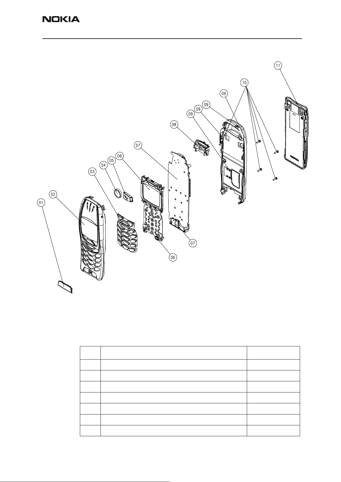
Figure 1 Exploded view of NPE-4
Table 1: List of main components
Item Description NMP code
01
02a
02b
02c
03
04
05
Logo Badge 9430274
A-cover Assembly Jet Black
A-cover Assembly Sirocco Bronze 9452191
A-cover Assembly Mistral Beige 9452190
Keymat 979........
Speaker
Buzzer Assembly 5140209
9451928
5140233
Original ãNokia Corporation. Page 1-5
Page 12
NPE-4
1 - General Information PAMS Technical Documentation
Table 1: List of main components
Item Description NMP code
06
07
08
09a
09b
09c
09d
10
11
Integrated BLUETOOTH
Bluetooth is a global standard for wireless connectivity. Bluetooth technology is based
on a low-cost, short-range radio link that operates in the globally available ISM (Industrial Scientific Medical) frequency band at 2.4 GHz.
As a widely adopted open standard, Bluetooth is intended for use in mobile phones, laptops, printers, digital cameras and other devices.
Lightguide Assembly, 4850163
Microphone + Boot Assembly 5140225
Antenna – Internal Antenna Plated 0660231
B-cover Assembly 9458087
Sim slide 9510467
On/off key 9790412
Volume key 9790385
Screw M1.6 x 5.5 6150025
Battery BPS-2 0670354
Bluetooth in the NPE-4 (Nokia 6310)
The integrated Bluetooth module (containing a Bluetooth transmitter and receiver)
allows the user to connect wirelessly to other Bluetooth devices within a range of 10
meters. The main uses of the Bluetooth module in the NPE-4 (Nokia 6310) are:
• Synchronisation of phonebook and calendar information between the NPE-4
(Nokia 6310) and a compatible PC. Calendar synchronisation works between the
phone and, for example, Microsoft Outlook or Lotus Notes using Nokia PC Suite.
• Wireless data (dial-up) connections. Laptop users can access the Internet and
handle e-mail by connecting the laptop to a computer network via Bluetooth and
the NPE-4 (Nokia 6310). The phone will work as a wireless modem.
• Wireless audio based on Bluetooth, allowing users to be wireless with Nokia
Bluetooth audio accessories (headset and car kit).
• Sending of business cards and calendar notes to e.g. another NPE-4 (Nokia 6310).
WALLET
The new wallet feature in the NPE-4 (Nokia 6310) enables users to make on-line transactions via a WAP browser, using your credit card to pay for books and tickets, for instance.
The wallet is a password-protected "locker" in your phone containing your credit card
information and other private information. When you want to buy something via WAP
and are asked for your credit card data, you only need to select wallet and give your
password, instead of keying in all of the information manually.
Page 1-6 ãNokia Corporation. Original
Page 13

NPE-4
PAMS Technical Documentation 1 - General Information
Benefits
• Fast, convenient and secure on-line transactions via WAP
• Secure storage for your personal information inside the phone, e.g. for user
names, passwords and numbers
• Protected storage inside the phone using the Wallet code for access
• Easy-to-use
• One step towards a Personal Trusted Device
GPRS (GENERAL PACKET RADIO SERVICE)
Mobile on-line
GPRS is a new feature in the existing GSM network. GPRS sends and receives your data
in ’packets’ - small packages of data that are sent across the network and then reassembled at the destination.
GPRS is different from traditional circuit switched services because the information is
broken down into IP (Internet Protocol) packets. IP Packet data is more efficiently routed
across the network and uses less network resources, which reduces the cost to the end
user.
GPRS enables users to have an always online mobile access to operator services and the
Internet. The main use for GPRS in the beginning will be as a bearer for WAP services, but
GPRS can also be used for data (dial-up) connections and for SMS messaging.
The charging (billing) will be based on how much data you send and receive and not on
how long time you have been connected.
Benefits with GPRS
• you can be always online
• data are more efficiently routed across the network
• you are charged according to the amount of data that you send and receive
• immediate access to WAP services
Before you can use GPRS
• you need to subscribe to GPRS (for availability and subscription to GPRS, contact
your network operator or service provider)
• set up your phone and/or PC to use GPRS
GPRS data speeds
The data transfer speed of a GPRS connection can (at the moment) be up to 40.2 kbps.
The speed depends on the network capacity and may change from moment to moment.
Original ãNokia Corporation. Page 1-7
Page 14

NPE-4
1 - General Information PAMS Technical Documentation
Comparisons: Normal WAP connection: 9.6 or 14.4 kbps
Normal GSM data conn.:9.6 or 14.4 kbps
High speed data conn.:up to 43.2 kbps
GPRS WAP connection:up to 40.2 kbps
GPRS data connection:up to 40.2 kbps
WAP
WAP IN THE NPE-4 (Nokia 6310)
The WAP feature in the NPE-4 (Nokia 6310) is very much like the WAP feature seen in
previous Nokia phones like the Nokia 6210. Main differences are
• GPRS - a new feature that can be used as a data bearer for WAP
• The WAP version is new (version 1.2.1) and it includes new functions
THE NEW FEATURES IN WAP
Push Service message indicator
The NPE-4 (Nokia 6310) can receive a service message with a short header and a link to
a specific WAP service. The type of messages that you want to subscribe to can be
selected from operators or service providers according to personal interest.
WAP push messages are stored in a dedicated service inbox. This inbox is found in the
Services menu. While online, the service inbox is found under the Options. You can anytime connect to the link that is included in a service message.
When a new WAP push message (with priority high or medium) is received, a notification
"New service message received" is displayed. You can read the message or discard the
notification. You can save 10 messages in the service inbox.
WAP push message is automatically removed from the service inbox when expiry time
(set by the content provider) is reached.
Direct calling (WTAI - Wireless Telephony Applications Interface)
WTAI enables interaction between the WAP browser and other parts of the mobile
phone. For example it will be possible to call directly from a phone book on a WAP page
by selecting the number to call. The WAP page must be designed to support this feature.
Cookies
Works similarly to the Internet cookies. A server can store a text-string in the phone,
making it possible for a WAP-service to recognise the user from time to time, creating a
more personal and easier browsing. The NPE-4 (Nokia 6310) has memory for 20 cookies,
that will be outdated starting from the last used ones.
Page 1-8 ãNokia Corporation. Original
Page 15

NPE-4
PAMS Technical Documentation 1 - General Information
Downloadable Calendar (vCal) and Contact (vCard) items
Calendar appointments and business cards can be saved to the phone’s calendar or
phone book. E.g. while browsing you can select a calendar event or a business card on a
WAP page to be saved into the phone’s memory.
Direct editing
When the cursor is on top of a link to an input box, pressing the numeric keypad will
immediately start inputting into the editor. There is no need to press the select key to get
to the editor.
Voice commands and recording features
The voice features have been extended with voice commands and a voice recorder.
With voice commands you can operate up to five features (e.g. change profile) by speaking a voice tag of your choice.
The NPE-4 (Nokia 6310) has a voice recorder that can hold a total of 3 minutes of
recordings. The recorder can e.g. be used for making spoken memos.
For voice dialling ten phone numbers in the phone book can have a voice tag attached.
Original ãNokia Corporation. Page 1-9
Page 16
NPE-4
1 - General Information PAMS Technical Documentation
Accessories
Accessory Type No.
Chargers Multivoltage (Travel) ACP-8
Multivoltage (Travel) ACP-9
Standard ACP-7
Mobile LCH-9
Batteries Li-Pol 1100 mAh Ultra Slim BPS-2
LI-Ion 1050 mAh Slim BLS-2N
Ni-MH 900 mAh Standard BMS-2S
Desktop Stand DCH-9
Car Accessories Advanced HF Car kit CARK-91
Phone Holder MBC-1
Handset (E & A) / Privacy Handset (APAC) HSU-1
Antenna Set NMT/GSM AMD-2
Personal Headset HDC-9P
Leather pouch CBL-5,
CSP-1
Mobile Inductive Loopset LPS-1
RS-232 Adaptive (data) Cable DLR-3P
Nokia PC Suite Ver. 4.5
External Antenna Cable XRC-1
Bluetooth Headset HDW-1
Wireless Car Kit CARK-112
Nokia PC Connectivity Card DTL-4
Page 1-10 ãNokia Corporation. Original
Page 17

Programmes After Market Services
NPE-4 Series Cellular Phones
2 - Broadband System
Original ãNokia Corporation. Page 2-1
Page 18

NPE-4
2 - Broadband System PAMS Technical Documentation
Table of Contents
Description Page No.
Introduction ......................................................................................................................................
Abbreviations .................................................................................................................................... 5
Environmental specification ......................................................................................................... 7
Absolute maximum ratings .................................................................................................... 7
Normal and extreme voltages ............................................................................................... 7
Temeperature conditions ........................................................................................................8
Humidity and water resistance ............................................................................................. 8
Vibration and bump ................................................................................................................. 8
EMC / ESD immunity ............................................................................................................... 8
Technical specifications ................................................................................................................. 8
UEM .............................................................................................................................................. 8
Reset sequence .................................................................................................................. 8
No supply ............................................................................................................................. 10
Backup .................................................................................................................................. 11
Power off ............................................................................................................................ 11
Reset .................................................................................................................................... 11
Power on ............................................................................................................................. 11
Sleep .................................................................................................................................... 11
Protection mode ...............................................................................................................12
DC characteristics ................................................................................................................... 12
Charging .................................................................................................................................... 15
Battery ........................................................................................................................................ 18
UPP (Universal Phone Processor) ........................................................................................ 19
Bluetooth ................................................................................................................................... 21
Ul .................................................................................................................................................. 21
LCD cell ............................................................................................................................... 21
LCD Backlight .................................................................................................................... 23
Keyboard light ................................................................................................................... 24
LED driver circuit .............................................................................................................. 24
Vibra .................................................................................................................................... 24
Buzzer ................................................................................................................................. 24
Keypad ................................................................................................................................ 25
IR-module .................................................................................................................................. 25
SIM .............................................................................................................................................. 25
Memory description ....................................................................................................................... 26
Read cycle ................................................................................................................................. 27
Write cycle ................................................................................................................................ 27
Power saving signal (PS) ........................................................................................................ 28
Memory block ........................................................................................................................... 30
Block locking ............................................................................................................................ 30
Read while write (RWW) ....................................................................................................... 31
Burst mode ................................................................................................................................ 32
5
Page 2-2 ãNokia Corporation. Original
Page 19

NPE-4
PAMS Technical Documentation 2 - Broadband System
Description Page No.
Flash programming ................................................................................................................. 32
MCU boot .................................................................................................................................. 33
Flash identifiers ....................................................................................................................... 33
First word ........................................................................................................................... 33
Second word ...................................................................................................................... 33
Third word .......................................................................................................................... 33
Fourth word ....................................................................................................................... 33
Fifth word ............................................................................................................................ 34
Absolute maximum ratings (AMD 64bit) ........................................................................... 34
Absolute maximum ratings (INTEL 64bit) .......................................................................... 34
HW Interfaces .................................................................................................................................. 35
Keypad interface ...................................................................................................................... 35
LCD interface ............................................................................................................................ 36
SIM interface ............................................................................................................................ 37
Ostrich ........................................................................................................................................ 38
JTAG interface .......................................................................................................................... 38
BT module interface ................................................................................................................ 39
SW interface ...................................................................................................................... 39
BT102 flash programming ............................................................................................. 39
HW interface ..................................................................................................................... 40
Baseband - RF interface ........................................................................................................ 42
Digital signals ................................................................................................................... 42
Analogue signals ..............................................................................................................44
Voltage supplies and references .................................................................................. 48
Accessory interfaces ............................................................................................................... 49
MBus ........................................................................................................................................... 49
FBus ............................................................................................................................................. 50
Baseband EMC strategy ................................................................................................................ 50
EMC design ............................................................................................................................... 51
SIM and keypad ................................................................................................................52
ESD test ...................................................................................................................................... 52
Conducted and radiated immunity tests ............................................................................ 53
TDMA noise ............................................................................................................................... 53
Baseband testing ............................................................................................................................ 53
Test Points .......................................................................................................................................... 53
List of Figures
Figure 1 NPE-4 Baseband block diagram ............................................................................ 6
Figure 2 UEM state disgram .................................................................................................... 9
Figure 3 LCD worst case test image ...................................................................................... 13
Figure 4 Baseband power distribution ................................................................................. 15
Figure 5 Charging configuration ............................................................................................ 15
Figure 6 Detection of charger ................................................................................................. 16
Original ãNokia Corporation. Page 2-3
Page 20

NPE-4
2 - Broadband System PAMS Technical Documentation
Description Page No.
List of Figures (continued)
Figure 7 UEM charging state diagram, PWM mode only ................................................ 17
Figure 8 Charging scenario where the battery is abruptly removed ............................ 18
Figure 9 Mechanical layout of DCT-3 battery .................................................................... 19
Figure 10 UPP architecture ........................................................................................................ 20
Figure 11 Complete overview of LCD module ....................................................................... 22
Figure 12 LCD module ................................................................................................................. 23
Figure 13 LED driver circuit for display and key light ......................................................... 24
Figure 14 NPE-4 IR connectivity ............................................................................................. 25
Figure 15 UPP, UEM and SIM connections ............................................................................ 26
Figure 16 Basic reading (random access) ............................................................................... 27
Figure 17 Write waveform (random access) ......................................................................... 28
Figure 18 The data is compared by using an XOR-function ............................................. 29
Figure 19 The comparison shows more unequal bits .......................................................... 30
Figure 20 Burst mode reading from the flash ....................................................................... 32
Figure 21 NPE-4 keypad ............................................................................................................ 35
Figure 22 Placement of SIM pins (phone bottom view) ..................................................... 37
Figure 23 SW interface diagram ............................................................................................... 39
Figure 24 BT102 Flash programming ...................................................................................... 39
Figure 25 BT102 HW interface .................................................................................................. 40
Figure 26 XEAR connection .......................................................................................................51
Figure 27 XMIC connection ....................................................................................................... 52
List of Tables
Table 1 Absolute max. ratings ............................................................................................... 7
Table 2 Temperature conditions for NPE-4 ...................................................................... 8
Table 3 UEM regulator outputs and state in SLEEP ........................................................ 12
Table 4 NPE-4 current consumption from VFLASH during SLEEP mode .................. 13
Table 5 LCD current consumption ........................................................................................ 23
Table 6 Absolute max. ratings for AMD 64Mbit .............................................................. 34
Table 7 Absolute max. ratings for Intel 64Mbit ............................................................... 34
Table 8 LCD module pin-out to PWB .................................................................................. 36
Table 9 SIM connector interface .......................................................................................... 37
Table 10 Ostrich interface ........................................................................................................ 38
Table 11 JTAG interface levels ................................................................................................. 38
Table 12 BT - BB interface description ................................................................................. 40
Table 13 Digital signals ............................................................................................................. 43
Table 14 Analoge signals .......................................................................................................... 44
Table 15 Regulators and references ....................................................................................... 48
Table 16 MBus interface .......................................................................................................... 50
Table 17 FBus interface ............................................................................................................ 50
Page 2-4 ãNokia Corporation. Original
Page 21

NPE-4
PAMS Technical Documentation 2 - Broadband System
Introduction
This Chapter specifies the baseband module for the NPE-4 program. The baseband module includes the baseband engine chipset, The UI components and the acoustical parts
for the transceiver.
NPE-4 is a hand-portable GSM900/GSM1800 phone for the classic segment, having the
DCT4 generation baseband- and RF circuitry. The key drivers for this product are GPRS
data transmission and short time to market.
The mechanical solution is based on the NPE-3 phone, modified with a new A-cover
design. The acoustical design is very similar to that implemented in NPE-3.
NPE-4 is having the DCT3 system connector and supports accordingly most DCT3 accessories. The battery interface is the one known from DCT3 phones and NPE-4 will support
both Nickel- and Lithium batteries.
New features in NPE-4 project is Bluetooth wireless data and audio connection and
GPRS for TCP/IP protocol data transmission.
Abbreviations
BSI Battery Size Indicator
NO_SUPPLY UEM state where UEM has no supply what so ever
VBAT Main battery voltage
V
VBACK Backup battery voltage
V_BU
BACK_UP UEM state where UEM has backup voltage
RESET UEM state where regulators are enabled
RTC UEM internal Real Time Clock
VRTC Regulator voltage for RTC
PWR_OFF UEM state where phone is off
SLEEP UEM power saving state controlled by UPP
SLEEPX SLEEP control signal from UPP
PWRONX Signal from power on key. '1' = key pressed.
VCHAR Charger input voltage
MSTR+
COFF+
, V
MSTR-
, V_BU
COFF-
Master Reset threshold level (2.1 V / 1.9 V)
Backup battery threshold level (3.1 V / 2.8 V)
VCHAR
DET
Charger detection threshold level
UEM Universal Energy Management
UPP Universal Phone Processor
IMD In-Mould Decoration
Original ãNokia Corporation. Page 2-5
Page 22
NPE-4
2 - Broadband System PAMS Technical Documentation
Technical Summary
PA Supply
RF Supplies
RF RX/TX
IRDA
EAR
MIC
BUZZO
VIBRA
M
Battery
UEM
Baseband
DLIGHT
KLIGHT
SLEEPCLK
32kHz
BB
Supplies
MBus/FBus
External Audio
Charger connection
CBUS/
DBUS
UI
UPP
MEMADDASIMIF
SIM FLASH
13MHz
HAGAR
26MHz
CBUS
USART
Bluetooth
DCT3 System connector
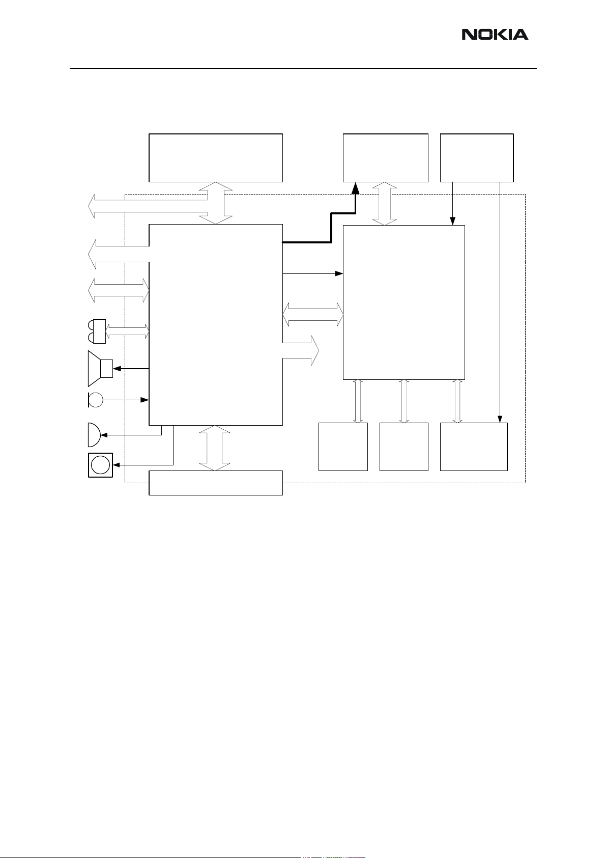
Figure 1 NPE-4 baseband block diagram
A draft block diagram is shown in Figure 1 NPE-4 baseband block diagram.
The baseband module contains 2 ASICs namely the Universal Energy Management (UEM)
and the Universal Phone Processor (UPP). The baseband module furthermore contains the
Bluetooth module. The baseband is based on the DCT4 engine program.
The UEM supplies both the baseband module as well as the RF module with a series of
voltage regulators. The RF module is supplied with regulated voltages 4.75 V and 2.78 V
and the baseband module with 2.78 V and 1.80 V. The UEM is furthermore supplying the
baseband SIM interface with a programmable voltage of either 1.8 V or 3.0 V and the
core of the UPP is supplied with a programmable voltage of 1.0 V, 1.3 V, 1.5 V or 1.8 V.
The UEM contains a series of PWM sourced drivers. The individual PWM signals are generated internally within the digital part of the UEM and distributed to the drivers. The
Page 2-6 ãNokia Corporation. Original
Page 23
NPE-4
PAMS Technical Documentation 2 - Broadband System
buzzer driver receives a PWM signal where both frequency and duty-cycle are pre-set by
register writings. For the vibra, a set of frequencies can be chosen. The frequencies are 64
Hz, 128 Hz, 258 Hz and 520 Hz and the duty cycle 2.9 % to 96.9 %. LCD and keyboard
light LED drivers receive a PWM signal of 128 Hz where the duty-cycle can be programmed by setting a 4-bit register.
The UEM also contains an IR driver supporting 9600 bps to 1152 kbps, semi duplex. This
driver works as a level shifter on the RX and TX lines to and from the UPP.
The UEM contains a real-time clock sliced down from the 32768 Hz crystal oscillator. The
32768 Hz clock is fed to the UPP as a sleep clock.
The communication between the UEM and the UPP is done on the bi-directional CBUS
and DBus. The CBUS is controlled by the MCU and can operate at a speed of maximum 1
MHz. The DBus is controlled by the DSP and can operate at a maximum speed of 13 MHz.
Both processors are located in the UPP.
Environmental Specifications
Absolute maximum ratings
Table 1: Absolute maximum ratings
Parameter Rating Remarks
Supply voltage, VBAT -0.3 V - 5.5 VDC Supply voltage for UEM
Charger input voltage, VCH -0.3 V - 16 VDC Conditions set by UEM. Input
clamped @16 VDC.
, Hardware cut-off voltage)
, Upper charger limit)
Normal and extreme voltages
Nominal voltage: 3.6 V (VBAT, Main battery voltage)
Lower extreme voltage: 2.9 V (V
Higher extreme voltage 5.4 V (VBAT
-0.3 – 20 VDC
pk
COFF-
LIM2+
Conditions set by UEM.
Minimum guarantied
operating voltage 3.04 V (DCT4 Engine minimum cut-off voltage)
Original ãNokia Corporation. Page 2-7
Page 24
NPE-4
2 - Broadband System PAMS Technical Documentation
Temperature Conditions
Table 2: Temperature conditions for NPE-4
Environmental condition Ambient temperature Remarks
Normal operation
Reduced performance
No operation or storage
Long term storage
conditions
-25 ° C … +55 °C
+55 °C … +70 °C
-40 °C > T > 85 °C
Humidity and water resistance
The baseband module will comply with the SPR4 Operating Conditions.
Vibration and bump
The baseband module will comply with the SPR3 Mechanical Functionality.
EMC / ESD immunity
The baseband module will comply with the SPR4 Operating Conditions. See also baseband EMC strategy in section Baseband EMC Strategy on page Baseband EMC Strategy.
Technical Specifications
0 °C … +40 °C
Specifications fulfilled
Operational for short periods only
No storage. An attempt to operate may
damage the phone permanently
Condition is without battery
The following chapters describe the NPE-4 baseband module in overview. If further information is needed, check with the references at the end of the Specification section References and/or with references mentioned in the individual chapters.
UEM
The UEM is one of the two ASICs in the baseband module.
Reset sequence
The functional behaviour of the UEM can be divided into 7 different states. Since the
UEM controls the regulated power distribution of the phone, each of these states affects
the general functionality of the phone:
• No supply
•Backup
•Power off
•Reset
•Power on
•Sleep
•Protection
Page 2-8 ãNokia Corporation. Original
Page 25
NPE-4
PAMS Technical Documentation 2 - Broadband System
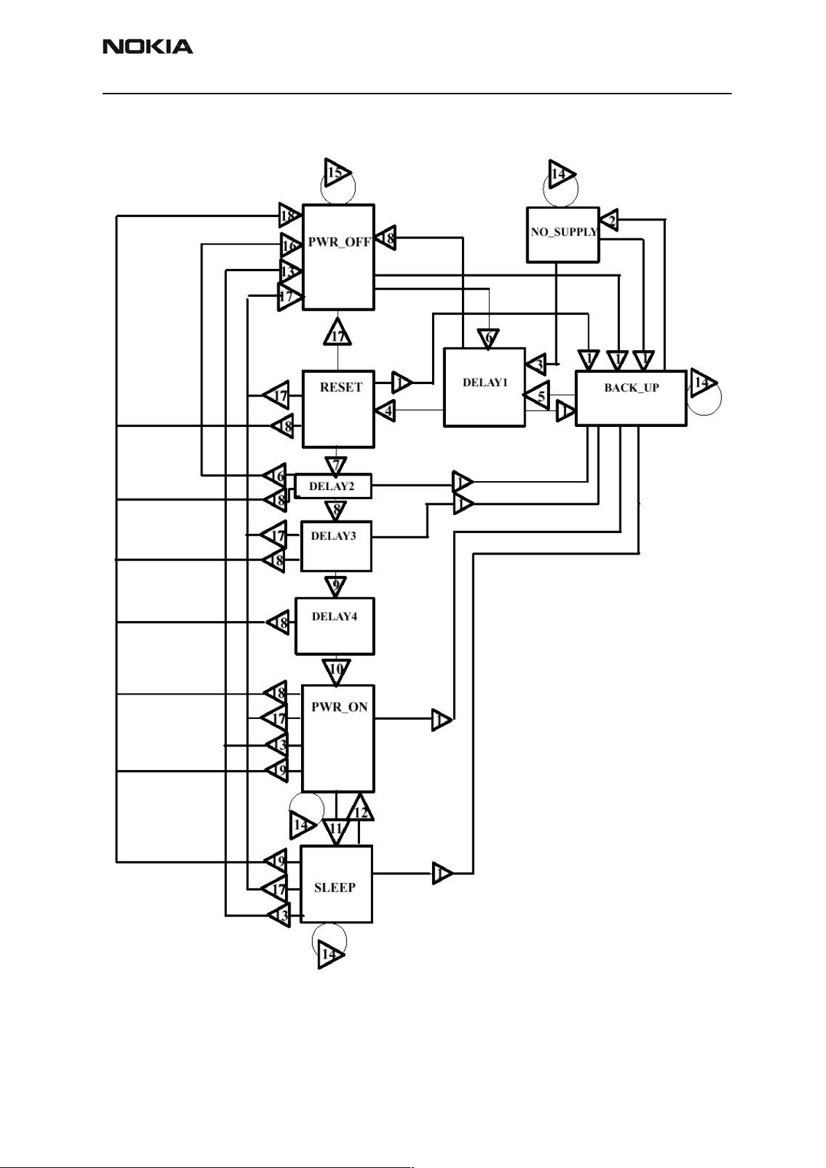
Figure 2 UEM state diagram
Original ãNokia Corporation. Page 2-9
Page 26

NPE-4
2 - Broadband System PAMS Technical Documentation
The text below explains the state diagram. The symbol 'ä' means that the voltage rises
and 'æ' that the voltage drops. '®' Means the result of the conditions set on the left
most side.
VBAT < V
VBAT < V
VBAT ä V
VBAT > V
VBAT ä V
and VBACK > V_BU
MSTR
and VBACK < V_BU
MSTR
. VBACK < V_BU
MSTR+
. DELAY1 elapses ® Go to RESET
MSTR
. VBACK > V_BU
MSTR+
COFF
COFF
PWRONX = '0' or VCHAR ä VCHAR
VBAT > V
® Go to DELAY2
COFF+
DELAY2 elapses ® Go to DELAY3
VBAT > C
. DELAY3 elapses ® Go to DELAY4
OFF+
DELAY4 elapses ® Go to PWR_ON
SLEEPX = '0' ® Go to SLEEP
SLEEPX = '1' ® Go to PWR_ON
® Go to BACK_UP
COFF
® Go to NO_SUPPLY
COFF
® Go to DELAY1
® Go to DELAY1
or ALARM = '1' ® Go to DELAY1
DET+
VBAT æ V
No change
VBAT > V
PWRONX ä detection during DELAY2 ® Go to PWR_OFF
Watchdog elapses (approx. 100 ms) ® Go to PWR_OFF
Thermal shutdown ® Go to PWR_OFF
PwrKeyWatchdog (4 sec.) elapses ® Go to PWR_OFF
The different states of the UEM are explained further below:
No supply
In the NO_SUPPLY mode the UEM has no supply voltage (VBAT < V
V_BU
tery is either disconnected or both discharged to a low voltage level.
The UEM will recover from NO_SUPPLY into RESET mode if the VBAT voltage level rises
above the V
and VBAT > V
COFF-
® Stay in PWR_OFF
MSTR
). This mode is due to the fact, that both the main battery and the backup bat-
COFF-
level by either reconnecting the main battery or charge it to such level.
MSTR+
® Go to PWR_OFF
MSTR-
and VBACK <
MSTR
Page 2-10 ãNokia Corporation. Original
Page 27

NPE-4
PAMS Technical Documentation 2 - Broadband System
Backup
In BACK_UP mode the main battery is either disconnected or has a low voltage level
(VBAT < V
and VBACK > V_BU
MSTR-
COFF+
).
The regulator VRTC that supplies the real time clock is disabled in BACK_UP mode.
Instead the unregulated backup battery voltage VBACK supplies the output of the VRTC.
All other regulators are disabled and the phone has no functionality.
The UEM will recover from BACK_UP mode into RESET mode if VBAT rises above V
Power off
In order for the UEM to be in PWR_OFF mode, it must have supply voltage (VBAT >
V
The regulator VRTC regulator is enabled and supplying the RTC within the UEM. The UEM
will enter RESET mode after a 20 ms delay whenever one of the below listed conditions is
logically true:
The UEM will enter PWR_OFF from all other modes except NO_SUPPLY and BACK_UP if
the internal watchdog elapses.
Reset
).
MSTR+
• The power button is activated
• Charger connection is detected
• RTC alarm is detected
MSTR+
.
When the UEM enters RESET mode from PWR_OFF mode the watchdog is enabled. If the
VBAT fails to rise above the power-up voltage level V
elapses, the UEM will enter PWR_OFF mode. Otherwise after a 200 ms delay the regulator VFLASH1 will be enabled and after a additional delay of 500 ms the regulators VANA,
VIO, VCORE and VR3 will be enabled. All other regulators i.e. VFLASH2, VSIM, VR1, VR2
and VR4 – VR7 are software controlled and disabled by default. After an additional delay
of 20 ms the UEM enters PWR_ON mode.
Power on
In PWR_ON the UEM is fully functional in the sense that all internal circuits is powered
up or can be by means of software. The UEM will enter PWR_OFF mode if VBAT drops
below V
PWR_OFF mode if either of the watchdogs Operational State Machine (approx. 100 ms),
Security (32 sec.) or Power Key (4 sec.) elapses or if any of the regulators triggers the
thermal protection circuitry
Sleep
The UEM can be forced into SLEEP mode by the UPP by setting the input SLEEPX low for
more than 60 ms. This state is entered when the external UPP activity is low (phone in
(3.1 V) before the watchdog
COFF+
for a period of time longer than 5 ms. The UEM will furthermore enter
COOF-
Original ãNokia Corporation. Page 2-11
Page 28
NPE-4
2 - Broadband System PAMS Technical Documentation
sleep) and thereby lowering the internal current consumption of the UEM. The regulator
VANA is disabled and VR1 – VR7 are either disabled or in low quiescent mode.
From SLEEP the UEM enters PWR_ON if SLEEPX goes high, PWR_OFF mode if watchdog
elapses or BACK_UP mode if VBAT drops below V
MSTR-
.
Protection mode
The UEM has two separate protection limits for over temperature conditions, one for the
charging switch and one for the regulators. The temperature circuitry measures the onchip temperature. In case of charging over temperature, the circuit turns the charging
switch off. In case of over temperature in any of the regulators, the UEM powers off.
DC characteristics
The figures in the following table reflect the specifications of the voltage and current
regulators within the UEM.
Table 3: UEM regulator outputs and state in sleep
Regulator Tar get Output Voltage [V] Output Current [mA]
Min Typ Max Min Max
VR1A, VR1B RF 4.6 4.75 4.9 0 10 Off
6
VR2
VR3 RF 2.70 2.78 2.86 0.1 20 Off
2
VR4
VR5, VR6
VR7 RF 2.70 2.78 2.86 0.1 45 Off
VrefRF01 RF 1.334 1.35 1.366 - 0.1 On
VrefRF02
VIO
VSIM
VANA BB 2.70 2.78 2.86 0.005 80 Off
VCORE
VFLASH1 BB 2.70 2.78 2.86 0.005
VFLASH2
2
1
2
2
3
5
RF 2.70 2.78 2.86 0.1 100 Off or Low Iq
RF 2.70 2.78 2.86 0.1 50
0.1
RF 2.70 2.78 2.86 0.1 50
0.1
RF 1.323 1.35 1.377 - 0.1 On or Off
BB 1.72 1.8 1.88 0.005
0.005
BB 1.745
2.91
BB 1.000
1.235
1.425
1.710
0.974
1.215
1.410
1.692
BB 2.70 2.78 2.86 0.005 40 On or Off
1.8
3.0
1.053
1.3
1.5
1.8
1.053
1.3
1.5
1.8
1.855
3.09
1.106
1.365
1.575
1.890
1.132
1.365
1.575
1.890
0.005
0.005
0.005
0.005
0.005
0.005
70
85
100
120
0.005
150
0.500
25
0.500
70
85
100
120
200
200
200
200
70
1.5
UEMSLX = '0'
Off
Off
Low Iq
Low Iq
Low Iq
Low Iq
4
Page 2-12 ãNokia Corporation. Original
Page 29
NPE-4
PAMS Technical Documentation 2 - Broadband System
1) Controlled by MCU writing to UEM references register.
2) The second current value indicates the maximum possible output current of the
regulator when in low quiescent mode.
3) The output voltages are split into two different current categories. The upper part
is the lower range of output current, and the lower part is the higher range of
output current.
4) UEMSLX is slave to SleepX from the UPP. Sets the UEM into sleep mode.
5) Condition in sleep-mode depends on MCU writings to UEM regulator registers
solely.
6) Condition in sleep-mode depends on DSP writings to UEM register.
Due to the low output current from the VFLASH1 regulator during sleep, the following
table with estimated current consumption drawn from the regulator in sleep mode was
made.
Table 4: NPE-4 current consumption from VFLASH1 during Sleep mode
Consumer Max current
1
LCD
Audio area
- XMIC
- XEAR
- DLR-3P
Bluetooth 8
UEM
- 2 x slow ADC
- BSI
IR 5
Total 482
376 mA All figures are estimates @25 °C
60
1
1
2
29
Unit
Note
1) Maximum current measured on 10 samples.
The current consumed by the LCD has been measured by vendor using worst case normal
mode displayed image as shown in Figure 3.
Figure 3 LCD worst case test image
Original ãNokia Corporation. Page 2-13
Page 30

NPE-4
2 - Broadband System PAMS Technical Documentation
Under normal conditions, the battery powers the baseband module. The battery voltage
VBAT is regulated by individual regulators located within the UEM. These regulators supply the different parts of the phone. 8 regulators are dedicated to the RF module of the
phone, and 6 to the baseband module.
The VSIM regulator is able to deliver both 1.8 and 3.0 Vdc and thus supporting two different SIM technologies. A register internally in the UEM controls the output of VSIM
and can be written to by the MCU via the CBUS. The regulator VCORE is likewise adjustable and controlled by register writings by the MCU. VCORE supplies the core of the UPP
and can be adjusted on the fly by the MCU if DSP capacity is inadequate. Higher VCORE
supply (1.8 V) results in faster core operations in the UPP.
The regulator VFLASH2 supplies audio circuitry and is controlled by the MCU
The regulators VANA, VFLASH1 and VIO are solely controlled by the UEM and cannot be
en-/disabled by MCU writings. Furthermore, VFLASH1 and VIO are both ON, though in
low quiescent mode when the phone is in sleep mode. An output current of 500 mA can
be drawn from the VIO regulator and 1.5 mA from the VFLASH1 regulator. VIO supplies
the UPP, FLASH and LCD, VFLASH1 supplies LCD, DLR-3 cable, IRDA and the Bluetooth
module. VANA is supplying analogue parts internally in the UEM as well as the baseband
audio circuitry and pull-up resistors on the input of the UEM slow AD converters.
When the plug and play DLR-3 cable is connected to the phone, it must be supplied by
the phone with 2.78 Vdc / 25 mA. This is delivered via a switch from VFLASH1. The switch
is controlled by the MCU and the control signal originates from a general IO pin on the
UPP.
The regulators VR1A, VR1B, VR2 – VR7 and IPA1 – IPA4 are all controlled by the DSP via
the DBus. VR3 – VR7 are controlled by the UEM as well and are disabled in sleep regardless of DSP writings.
VBAT is furthermore distributed, unregulated, to the RF power-amplifier and the BT102
Bluetooth module as well as filters in the baseband module.
The CHACON module in the UEM controls the charging of the main battery. Furthermore
it contains a 3.2 Vdc regulator for charging of the backup battery and a 1.8 Vdc regulator
supplying the internal real time clock.
Page 2-14 ãNokia Corporation. Original
Page 31

NPE-4
PAMS Technical Documentation 2 - Broadband System
Baseband
UEM
RF Regulators
Boomer
VR1A
VR1B
VR2-7
6
SIM
VSIM
Battery
VCORE
VANA
VFLASH1
VFLASH2
VBAT
Bluetooth
PA Supply
Baseband
Regulators
RTC
CHACON
System Connecter
Figure 4 Baseband power distribution
VIO
UPP
FLASH
LCD
Backup
battery
DLR-3
switch
IRDA
Charging
The charging of the main battery is controlled by the UEM. External components are
needed in order to sense charging current and voltage that are needed by the Energy
Management (EM) software and to protect against EMC into the baseband area. The
charger is connected to the phone via the DCT3 bottom connector and routed from here
to the UEM via the PWB.
Transceiver
0R22
VBATREGS
1u10n
UEM
VCHARINVCHAROUT
CHACON
PWM
VCHAR
1n
10k
33R/100MHz
10k
10n
VCHAR
1.5A
CHRG_CTRL
GND
Figure 5 Charging configuration
Original ãNokia Corporation. Page 2-15
Charger
Filter
cap.
Zmin. 20k
Pull-
down
100k
1000uF
max.
Page 32

NPE-4
2 - Broadband System PAMS Technical Documentation
Connecting a charger to the telephone creates a voltage, VCH, on the UEM VCHAR input.
When the VCH level is detected to rise above the VCH
threshold (2.0 Vdc) by CHACON,
DET
charging starts. Level crossing detection of the VCHAR line is used to generate synchronizing pulses for UEM’s state machine for control of rectifier type chargers, e.g. ACP-7.
Figure 6 Detection of charger / generation of charger synchronization pulses
In case the main battery is fully discharged and the UEM subsequently is without power
i.e. in NO_SUPPLY or BACKUP mode, the start-up charging circuitry is in control, giving
the possibility to detect a charger and engage charging. If the VBAT level is detected to
be lower than the master reset voltage (V
with a constant current of 100 mA until VBAT exceeds V
) the CHACON will charge the battery
MSTR-
. When this happens, from
MSTR+
a charging point of view, normal PWM charging situation resumes. A PWM signal is generated by the digital part of the UEM, which sources the CHACON. The frequency of the
signal can be either 1 Hz or 32 Hz. If the connected charger is of a 2-wire kind e.g. ACP7, the PWM signal has the frequency 1 Hz. If the charger on the other hand is a 3-wire
type e.g. ACP-9, the switch is left on permanently and the 32 Hz PWM control signal
routed to the charger in order to produce a constant voltage. Figure 7 shows a state diagram of the PWM charge situation.
Page 2-16 ãNokia Corporation. Original
Page 33

NPE-4
PAMS Technical Documentation 2 - Broadband System
Figure 7 UEM charging state diagram, PWM mode only
In order to protect the phone from damage resulted by over voltage in the case that the
battery is abruptly removed when charging is ongoing, the charger switch is closed
immediately. This is detected by means of VBAT that will rise fast above VBAT
LIM1,2+
when the battery is removed. A scenario like this can be seen in Figure 8.
Original ãNokia Corporation. Page 2-17
Page 34

NPE-4
2 - Broadband System PAMS Technical Documentation
Figure 8 Charging scenario where the battery is abruptly removed
1) Battery disconnected abruptly during charging
2) VBAT reaches VBAT
LIM1,2+
3) VBAT falls below VBAT
4) VBAT reaches VBAT
LIM1,2+
5) VBAT falls below VBAT
® charging switch is turned off immediately
® charging switch is turned on (soft switching)
LIM1,2-
again ® charging switch is turned off
once again ® charging switch is turned back on
LIM1,2-
6) The PWM signal from the UEM digital part turns logical ´0´ because the system
has acknowledged the absence of a battery and this subsequently turns the
charging switch off.
7) VBAT falls below VBAT
LIM1,2-
but the charging switch is not turned back on since
the PWM signal is logical ´0´.
Note: that if the battery voltage level is below V
level when the battery is discon-
MSTR-
nected from the phone, and if the charger is still connected when the battery is
once again attached to the phone, the UEM will remain in NO_SUPPLY or
BACKUP mode. This will keep the phone OFF until the charger is first disconnected and then reconnected.
Battery
The battery is external and will be connected to the phone via four terminals as shown in
Figure 9. In order to detect the capacity and chemistry of the battery, the phone uses the
Page 2-18 ãNokia Corporation. Original
Page 35

NPE-4
PAMS Technical Documentation 2 - Broadband System
BSI connection in conjunction with 100 k_ pull-up resistors in the baseband module or in
the desk-stand DCH-9 extra battery slot, which allows charging of extra battery. 2.78 V
from VFLASH1 feeds the resistor in the baseband module and the resulting divided voltage is routed to the BSI ADC input in the UEM.
Figure 9 Mechanical layout of DCT-3 battery
The battery also contains a 47 k_ NTC resistor used for battery temperature measurements. The measurement of the temperature by means of resistors follows the same
principal as with the BSI resistor.
UPP (Universal Phone Processor).
The UPP used for NPE-4 is a version with 8 Mbit internally RAM. It is clocked by a 13MHz
frequency from the RF-chip "HAGAR".
It can operate on 4 different voltages; 1.05,1.3,1.5 and 1.8V. The voltage can be programmed "on the fly" by the SW. For example in standby-mode, 1.3V is used for power
saving, but in active-mode (i.e. call) the voltages is increased to 1.8V to get maximum
numbers of MIPS.
The UPP can be divided into two functional sections, Body and Brain. Body contains system logic, and Brain contains processor subsystem including DSP, MCU, memories and
Bus Controller. The function of the Body is mainly the same as in DCT3 system Logic. The
Body is connected to Brain via RHEA bus. The Body and Brain is shown below.
Original ãNokia Corporation. Page 2-19
Page 36

NPE-4
2 - Broadband System PAMS Technical Documentation
Figure 10 UPP architecture
Page 2-20 ãNokia Corporation. Original
Page 37

NPE-4
PAMS Technical Documentation 2 - Broadband System
The DSP inside the Brain is a Lead3 16–bit DSP core from TI (Texas Interments), with a
DMA controller, wait state generator and a program fetch of 32-bits. Furthermore, the
DSP core has an instruction-length flexibility of 8 to 48-bits. The maximum frequency
for the DSP core is 145MHz for the NPE-4 baseband, although the maximum frequency
for the core itself is 400 MHz. The core can do single and dual mac-operations per clockcycle. This means that the NPE-4 baseband has a maximum of 290 MIPS (mac-operations) on the DSP-core.
The DSP core has three different RAM-banks; cache RAM, dual access RAM for storing
and manipulating data and last, single access RAM for storing and manipulating SW
variables. All the RAM-banks have a 145 MHz clock and 32-bit organization. It has also
an ARM port interface, which is used for MCU/DSP message transfer (API).
The MCU consist of a 16/32–bit RISC core (ARM7). The block has a small ROM (768x32
bits) for MCU boot code. It interfaces to DSP through the 8Mbit PDRAM. The MCU has it
own sectors in the RAM as well as the DSP. RAM blocks or sectors are divided into the
following:
The rest of the PDRAM is used for program code, mainly GPRS SW.
Bluetooth
NPE-4 has a Bluetooth module BT102 that receives and transmit at 2.4GHz. The module
makes it possible for the phone to communicate via a radio link with other Bluetooth
units e.g. headsets, carkits or printers.
The Bluetooth module is itself made as a multilayer PWB – covering all the needed Asics
and discrete components – with a shielding frame- and lid. The module is soldered onto
the phone PWB in the same way as other SMD components.
UI
LCD cell
• 4 x 64Kbytes for the DSP and MCU.
• 4 x 64KB Banks, MCU only.
• 2 x 4KB Banks, for the DSP, and MCU.
The LCD is a black and white LS2 96x65 full dot matrix display. The LS2 display has a
standard DCT4 interface. The LCD cell consists of a single COG driver, 3 boosting capacitors and a FPC, where the capacitors are placed. The LCD interface between the LCD cell
and the main PWB can be viewed in section LCD Interface page LCD Interface.
The LCD cell is part of the complete LCD module, which includes metal frame, gasket,
light guide, spring connector, RTC battery, transflector (not shown) and dome sheet. The
figure below illustrates the complete overview of the LCD module.
Original ãNokia Corporation. Page 2-21
Page 38

NPE-4
2 - Broadband System PAMS Technical Documentation
Dome sheet
Light guide
Frame
Gasket
LCD
Figure 11 Complete overview of LCD module
Connector
"Displa
RTC Battery
Below is the general specifications listed:
• Glass size, width x height x thickness (incl. caps) : 38.4 mm x 37.6 mm x 2.75 mm
• Viewing area (width x height) : 35.4 mm x 27.7 mm
• Active pixel area (width x height) : 30.609 mm x 24.1 mm
• Number of pixels : 96 columns x 65 rows
• Pixel height to width ratio : 1.17:1
• Pixel gap : 0.015 mm
• Technology : FSTN
• Display type : Positive
• Main viewing direction : 6 o’clock
• Illumination Mode : Transflective
• Driver chip : DCT4 driver
Page 2-22 ãNokia Corporation. Original
Page 39

NPE-4
PAMS Technical Documentation 2 - Broadband System
Au Connector pads
C
FPC
C
SEG 0 SEG 95
COM 0COM 64
Figure 12 LCD module.
C
Driver
Viewing area
Active area
96 x 65
Top View
The LCD is powered from both V
FLASH1
and VIO. V
is used for the boosting circuit
FLASH1
and VIO for the driver chip. The total LCD current consumption specified by vendor is
described below:
Table 5: LCD current consumption
Typ Max Unit/Note
I
total
250 400
400
mA @ +25oC
I
total =IDD+IDDI
I
measured with normal mode test pattern.
total is
mA @ Top, measured with normal mode test
pattern.
900 1300
mA using worst case test pattern @25 °C
1
This test pattern is used for R&D purpose only and is not possible to recreate by end user.
LCD Backlight
The LCD backlight consists of 4 yellow/green LED's (NPE-3 type) which are placed on the
main PWB below the LCD area. They lit into the light guide where the light is distributed
to generate sufficient backlight for the LCD.
The LED driver circuit is shown below in Figure 13 LED driver circuit for display and key
light. The voltage drop over R307 produces a constant current of 40 mA, i.e. 10 mA pr.
LED (same as NPE-3).
The UEM output pin, DLIGHT, controls the driver circuit. This output is an open drain
driver. The output frequency is 128 Hz and the duty cycle can be changed from 0 – 100
% with 4 bit resolution. By changing the duty cycle of the PWM signal it is possible to
change the average current of the LED's.
Original ãNokia Corporation. Page 2-23
Page 40

NPE-4
2 - Broadband System PAMS Technical Documentation
Keyboard light
The keyboard light consists of 6 yellow/green LED's (NPE-3 type) which are placed under
the keyboard and use the light guide to distribute the light. The driver circuit is the same
as described above in section LCD Backlight, with the difference of a current of 60 mA,
i.e. 10 mA pr. LED.
The keyboard LED's can also be controlled by a 128 Hz PWM signal from the UEM,
KLIGHT.
LED driver circuit
V
BAT
LCD: R307 = 15R
KEY: R309/R310 = 10R
LCD: V311a
KEY: V313a
LCD: V311b
LCD: R306 = 1K
KEY: R308 = 1K
KEY: V313b
Vibra
Buzzer
x4 LEDs for LCD
DLIGHT
or
KLIGHT
x6 LEDs for key
Figure 13 LED driver circuit for display and key light.
A vibra-alerting device is used to generate a vibration signal for an incoming call. The
vibra is placed in the top of the phone. It is fastened to the A-cover by means of two
wings that are pressed into the A-cover.
The vibra is electrically connected to the PWB by spring contacts.
The vibra is controlled from the UEM by a PWM (Pulse Wide Modulated) square wave
signal.
Alerting tones and/or melodies are generated by a buzzer, which is controlled by a PWM
signal from the UEM. The SPL requirement is 105dB (A) at 5cm, however end of line
requirement from sup-supplier is 102dB at 5 cm.
The buzzer is designed to a first resonant peak at 2500 Hz. The ringer melodies will be
optimised in MCU so the main frequency of any given melody is shifted to near the resonant peak. For this optimisation a program called BuzzCalc will be used for the calculation of the dominating frequency of a given ringing melody or tone.
The design of the buzzer is a direct copy from the NPE-3 project. The Buzzer is glued to a
gasket. Vendor delivers this final assembly. Sound holes are placed in the A-cover
Page 2-24 ãNokia Corporation. Original
Page 41

NPE-4
PAMS Technical Documentation 2 - Broadband System
The buzzer is electrically connected to the PWB by spring contacts.
Keypad
See keypad interface in section Keypad interface on page Keypad interface.
IR-module
The IR module CIM-93M4 is fully compliant with the IrDA1.2.a and supports data rates
of 9600 bps to 1152 kbps. The module is connected to the UEM IR module, which acts as
a level-shifter between the IR module and the UPP. The UEM IR module supports the
data rates of the CIM-93M4.
VBAT
SIM
UPP
GenIO10
IRRX
IRTX
1.8 V
IRRX
1.8 V
IRTX
Figure 14 NPE-4 IR connectivity
UEM
IRLEDC
IRRXN
VFLASH1
V350
100k
2.78 V
2.78 V
LEDA
TXD
RXD
VCC
CIM-93M4
Hi/Low
Speed
CIM-93M4 operates on 2.7 V logic, thus the transistors. A future module will be operating by 1.8 V logic and the level shifter V350 in Figure 14, will be obsolete.
A metal shield covers the IR module in order to maximise performance in the high RF
field it operates in (Directly beneath the antenna).
NPE-4 uses a product specific SIM-card reader (SIM reader). Electrical connection of SIM
reader is similar to other DCT4 products. The SIM interface is split between UEM and UPP
(see Figure 7.14 UPP, UEM and SIM Connections below). This has been done in order to
reduce the amount of interconnections on the SIM interface between the UPP and the
UEM. The SIM interface control logic and UART is integrated into the UPP. The SIM interface start-up and power down sequence, including timing and reset generation is implemented in UEM. The SIM interface in the UPP supports the SIM speed enhancement
features, which improves the data transfer rate in the SIM interface.
The UEM contains the SIM interface logic level shifting. UPP SIM interface logic levels
are 1.8V. The SIM interface can be programmed to support 3V and 1.8V SIMs. A 5V SIM
interface is not supported. A register in the UEM selects the SIM supply voltage. It is only
allowed to change the SIM supply voltage when the SIM IF is powered down.
Original ãNokia Corporation. Page 2-25
Page 42

NPE-4
2 - Broadband System PAMS Technical Documentation
The SIM power up/down sequence is generated in the UEM. The Battery Type contact signal (BSI) is used to recognise if the battery suddenly is removed from the transceiver
block. The SIMCardDet is not used. If the BSI goes low, the power down sequence is
automatic initiated. The SIMIF will then force all the connections low, i.e. SIMRST, SIMCLK, SIMDATA and VSIM. A comparator inside the UEM does the monitoring of the BSI
signal. The comparator offset is such that the comparator output does not alter state as
long as the battery is connected. The BSI comparator threshold level is 2.1 V with 75 mV
hysteresis.
Figure 15 UPP, UEM and SIM Connections
Memory description
The NPE-4 baseband consists of 64Mbit (8MB) external flash memory. Access to the flash
is performed as 16-bit access in order to improve the data rate on the bus.
The purpose of the memory interface is to reduce the amount of connections by multiplexing the address and data bus on to the same signals. If the memory address space is
more than 16 bits, which is the case, then 16-bit data can be multiplexed on the address
inputs. This requires the memory to store the address during the first cycle in the access
as described in Figure 8.1 Basic reading (Random access).
In addition to this, the system provides a Power Save signal (PS), which is used to reduce
the switching on the external bus between the memory and the UPP. In case of writing to
the flash, the UPP provides the information on the PS signal, and in case data is read
from the flash, the memory provides the status of the PS signal. The PS signal is used to
indicate if data should be inverted at the receiver end. If PS = “1” the data shall be
inverted at the receiver end before it is stored/processed. The PS-signal will be described
more in details in section Power saving signal (PS)..
Page 2-26 ãNokia Corporation. Original
Page 43

NPE-4
PAMS Technical Documentation 2 - Broadband System
Furthermore the memory is capable of handle burst-mode (multiplexed address/databus) and memory blocking, which is controlled by the UPP.
Read cycle.
The read cycle is initiated by first applying the address to the multiplexed address/databus. The address is latched at the rising edge of the AVD-signal. The memory device captures the address/data bus-state at point B. The captured data is compared on a bit by bit
base (MSB–MSB, LSB–LSB), with the data inside memory. If the comparison shows more
equal bits than unequal bits, the data is not inverted before it is send out on the address/
data bus as output data. The result of the comparison is indicated, by using the PS signal
before the data is read (at point C) by the Bus Controller. This allows the receiving device
to invert the data before it is read into a register. The valid PS signal needs to be available in advance before the actual read operation takes place.
Figure 16 Basic reading (Random access)
Write cycle.
The write cycle is initiated by first applying the address to the multiplexed address/data
bus and to the address lines Axx-A16, (Axx is the MSB address for that memory density).
The address latch is transparent from A to B. The address is latched at the rising edge of
the AVD signal. Latching address Axx-A16 is mandatory. The random access time is mea-
Original ãNokia Corporation. Page 2-27
Page 44

NPE-4
2 - Broadband System PAMS Technical Documentation
sured from a stable address, falling-edge of AVD or falling-edge of CE which ever occurs
last. No clock is provided for a random access.
The below figure shows a basic write waveform.
Figure 17 Write waveform (Random access)
Power saving signal (PS).
In order to reduce the power consumption on the bus a Power Save function is introduced. This function reduces the amount of switching on the external bus.
Power is consumed in a digital system when a signal changes state. The power is consumed when the capacitive load is either charged or discharged. The capacitive load is
introduced by the interconnection itself and of cause by the input at the receiving
device. Internally in digital circuits the capacitive load is lower, than at the interconnect
level at the printed circuit board. Therefore it is an advantage if the amount of changes
on the external interconnection, i.e. between two digital circuits, can be minimised.
Therefore on a wide bus like an address/data bus in a microprocessor system, power is
saved, if the data to be transmitted on the external bus, causes a minimum amount of
transitions. This can be achieved by comparing the previously data on the bus, with the
data to be transmitted, and if inverting the data to be transmitted causes less transitions
to be performed on the external bus, the data is inverted, before it is output on the data
bus. To inform that the data is inverted, a control signal is used to inform the receiving
device, that the data must be inverted before any further processing.
Page 2-28 ãNokia Corporation. Original
Page 45

NPE-4
PAMS Technical Documentation 2 - Broadband System
Data on the address/data bus is bit wise compared which means that the data previously
on D0 (D0e) is compared with the new data to be output on D0 (D0i). If the two data elements are the same (D0e=D0i) a logic “0” is indicated to the comparing device. If the two
data elements are not the same (D0e=NOT(D0i)) a logic “1” is indicated to the comparing
device. If there are more equal signal than unequal signals on the address/data bus, the
new data is not inverted before it is sent out on the bus. If there are more unequal than
equal data on the address/data bus, the data is inverted before it is sent out on the bus.
The status whether the data that is presented on the address/data bus is inverted or not,
is indicated by a separate signal to the memory device. If the data on the bus is not
inverted this power control signal (PS), is at logic “0” state. If the data that is presented
on the bus is inverted, this is indicated by PS = logic “1”. This PS signal is a common signal for all the devices connected to the address/memory bus. The transmitting device
uses the PS signal to indicate non-inverted or inverted data. As only one device at a time,
can present data on the address/data bus, this signal is shared and only one additional
control signal PS is needed for the address/data bus, although the data bus may be connected to several devices. The below figure shows how this PS-signal actually works.
Figure 18 The data is compared by using an XOR-function. The result can be seen above.
In Figure 18 there are more equal bits than unequal bits, so therefor the data is not
inverted before it is sent out to the flash. This means that the PS-signal is "0". The next
scenario shows the opposite situation.
Original ãNokia Corporation. Page 2-29
Page 46

NPE-4
2 - Broadband System PAMS Technical Documentation
Figure 19 The comparison shows more unequal bits than equal bits,
and the bits are inverted on the bus.
The power save (PS) function is only active in burst mode due to delay in the readings
(Random access). If it were used in random access, it would have introduced a delay of
10 – 15 ns. The PS is not activated in the first access in the burst, only from the second
access in the burst.
In particular in burst mode it is important to keep the performance. In order to reduce
complexity in the memory, the power save function does not apply to the address. This
means that the address will always be presented in its true value. This means that the
memory do not have to manage the inversion of the address. In case of burst access it is
possible to reduce the power on the external bus by comparing the contents of the data
in the burst, not with the data on the bus. This results in that the random access data is
presented on the bus, as such but the following data in the burst is presented using the
power save function. By pipelining the power save information in this manner the additional delay caused by the comparison logic is removed.
Memory block.
The memory or flash is organised in four Banks, A, B, C and D. Bank A and B each contain
eight 8 Kword sectors and thirty-one 32 Kword sectors. Bank C and D each contain
thirty-two 32 Kword sectors. The total sector Architecture is eight 8 Kword sectors and
one hundred twenty-six 32 Kword sectors.
Block locking.
To prevent accidental writings to some of the sectors in the flash, block locking has to be
used. This can, depending on the vendor, bee implemented by using different methods.
AMD and Intel are the to only vendors that NPE-4 is going to use for the flash purpose.
AMD and Intel will implement their block locking in the following way.
Intel: The locking scheme offers two levels of protection. The first allows software-only
control of block locking (useful for frequently changed data blocks) while the second
Page 2-30 ãNokia Corporation. Original
Page 47

NPE-4
PAMS Technical Documentation 2 - Broadband System
requires hardware interaction before locking can be changed (protects infrequently
changed code blocks). For this purpose, a dedicated pin called WP is used. The WP-pin or
signal is only controlled by the hardware.
Lock block:
The blocks’ default power-up or reset status is locked. Locked blocks are fully protected
from alteration. Attempted program or erase operations to a locked block will return an
error in a status register inside the flash. A locked block’s status can be changed to
unlocked or lock-down using the appropriate software commands. Writing the "Lock
block command" sequence can lock an unlocked block.
Unlock block:
Unlocked blocks can be programmed or erased. All unlocked blocks return to the locked
state when the phone is or powered down. An unlocked block’s status can be changed to
the locked or locked-down state using the appropriate software commands. A locked
block can be unlocked by writing a "unlock block command" sequence, if the block is not
locked-down.
Lock-down block.
Locked-down blocks are protected from program and erase operations (just like locked
blocks), but software commands alone cannot change their protection status. A lockeddown block can only be unlocked when the WP-signal is high. When the WP-signal goes
low, all locked-down blocks revert to locked. A locked or unlocked block can be lockeddown by writing a "Lock-Down Block command" sequence. Locked-down blocks revert to
the locked state at device reset or power-down.
AMD:
a block a command sequence must be written, once the command unlock sequence is
written the SW can unlock as many blocks as required by entering the block address
while keeping a specific address high. If the address is taken to low, the block will be
locked instead of unlocked. The SW locking is similar to the Intel SW locking.
The AMD flash does also have the same hardware lock as Intel. The signal or pin is called
WP (write protect). The blocks are locked if WP is set to low. If the WP-signal is set high
then the SW can control the locking of the blocks. Finally, if the VPP pin is set to low all
blocks are locked.
It is not yet specified which flash type NPE-4 is going to use, but the SW-team has to
implement one of the above block-locking methods.
All blocks have a locking latch and upon power up all blocks are locked. To unlock
Read while Write (RWW).
The device is capable of reading data from one Bank of the memory while programming
or erasing in the other Bank of the memory. An erase operation may also be suspend to
read from or program to another location within the same Bank (except the sector being
erased).
Original ãNokia Corporation. Page 2-31
Page 48

NPE-4
2 - Broadband System PAMS Technical Documentation
Burst mode.
The flash device supports burst-mode. The purpose is to improve the date rate between
the flash and the UPP. The burst-mode can only be used for read operations. It is possible
to access the memory in burst-mode over the entire memory except for the 8 x 8 Kbytes
sectors. When using burst-mode at least 4 word (4*16 bits) is read from the flash. A read
operation from the flash, normally first set-up the address, and then the UPP will get the
data from this particular address. The address has to be set-up or sent to the flash ever
time the UPP wants to read from the flash. By using burst-mode the address only needs
to be sent one time, then flash will keep sending data as long as there is a clock-signal.
Figure 20 Burst-mode reading from the flash. Note that the address only is sent ones.
The flash keeps sending data to the UPP as long as the CS-signal and CLK are valid.
Flash programming.
The actual programming is indicated to the UPP by using the MBUS_RX signal between
the UPP and the UEM. The MBUS signal from the UEM to the flash prommer (FPS8 box) is
used as clock for the synchronous communication. The flash prommer keeps the MBUS
line low during UPP boot, to indicate that the flash prommer is connected. If the UPP
MBUS_RX signal is low on UPP, the MCU enters flash programming mode. If the signal is
high, the MCU starts loading software from the flash.
In order to avoid accidental entry to the "flash programming mode" the MCU only waits
for a specified time, to get input data from the flash prommer. If the timer expires without any data being received, the MCU will continue the boot sequence. The MBUS signal
from UEM to the external connection is used as clock during flash programming. This
means that flash programming clock is supplied to the UPP on the MBUS_RX signal. The
flash prommer indicates to the UEM that flash programming/reprogramming by writing
an 8 bit password to the UEM. The data is transmitted on the FBUS_RX line and the UEM
clocks the data on the FBUS_RX line into a shift register. When the 8-bits have been
shifted in the register, the FPS8-box generates a falling-edge on the BSI line. This loads
the shift register content in the UEM into a compare register. These 8-bits will be compared in a register to see if they match the "secret" default value inside the UEM. At this
point the flash prommer must pull the MBUS signal to UEM low, in order to indicate to
the MCU that the flash prommer is connected. The UEM reset-state machine performs a
reset to the system (PURX low for 10–100 ms). The UEM "flash programming mode" is
Page 2-32 ãNokia Corporation. Original
Page 49

NPE-4
PAMS Technical Documentation 2 - Broadband System
valid until MCU sets a bit in the UEM register, which indicates the "end of flash programming". Setting this bit also clears the compare register in the UEM previously loaded, at
the falling edge of the BSI signal. During the "flash programming mode" the UEM watchdog is disabled. When the bit is set it indicates "end of flash programming" and it resets
the UEM watchdog timer to it’s default value. Clearing the flash programming bit also
causes the UEM to generate a reset to the UPP. The BSI signal is used to load the value
into the compare register. In order to avoid spurious loading of the register, the BSI signal will be gated during UEM "master-reset", and during "power-on" when PURX is
active. The BSI signal should not change state during normal operation unless the battery is extracted, in this case the BSI signal will be pulled high, note a falling edge is
required to load the compare register.
MCU Boot.
When the MCU boots, it looks for flash programming indication by reading the status on
the MBUS signal. If this signal is pulled low the MCU sets up the UART in synchronous
mode, and indicates to the flash prommer, by setting FBUS_TX low, that it is ready to
accept the secondary boot-code. All flash programming related SW that is downloaded is
done so to the UPP internal MCU SRAM. The MCU also ends up in "flash programming
mode", if the contents of the flash is empty (reading FFH from the first memory location
in the flash).
Flash Identifiers.
Due to that DCT4 supports many different manufacturers; NMP needs to have so called
flash identifiers. The flash identifier tells the MCU which HW environment it is working
in, and also block size and configuration of the flash.
First Word.
The word contains the information about the number of flash devices connected to the
UPP. It is possible to setup the UPP so that it supports two devices. The MSB bit in the
word indicates the amount of flash devices used by the baseband. The amount of wait
states for the random access is specified over 3-bits in this word. The amount of wait
states is specified related to the system clock used in that system. The MCU PLL factor is
also specified in this word (2-bits).
Second Word.
This word contains information about flash sectors available for EEPROM emulation. If
no RWW capability is indicated, this field then contains information of the serial
EEPROM that is used in the system.
Third Word.
This word contains similar information as the first word but for the second flash if such
is used.
Fourth Word.
This word contains information about the sector configuration of the second flash.
Original ãNokia Corporation. Page 2-33
Page 50

NPE-4
2 - Broadband System PAMS Technical Documentation
Fifth Word.
This word contains information of the external SRAM if it is available on the baseband,
the size of it and the amount of wait states to be used when accessing it.
Absolute maximum ratings (AMD 64Mbit).
Table 6: Absolute maximum ratings for AMD 64 Mbit
Parameter Rating Remarks
Supply voltage (Vcc)
(operational voltage is: 1.7 –1.9)
VPP and RESET -0.5 V to +12.5
Output Short Circuit Current 100 mA No more than one output may be
Voltage with Respect to Ground.
All pins except VPP and RESET
-0,5 V to +4,0 Volt Minimum DC voltage on input or I/O
pins is -0.5 V
Minimum DC input voltage on pins
Volt
0.5 V to Vcc + 0.5
Volt
VPP, and RESET is -0.5 V
shorted to ground at a time. Duration
of the short circuit should not be
greater than one second.
Minimum DC voltage on input or I/O
pins is -0.5 V
Absolute maximum ratings (INTEL 64Mbit).
Table 7: Absolute maximum ratings for INTEL 64 Mbit
Parameter Rating Remarks
Voltage on any pin (except Vpp, Vpp) -0.5V to +2.45V See reference for details
Vpp Voltage -0.2V to +14V
Vcc and Vccq -0.2V to +2.45V
Output short circuit current 100mA
Page 2-34 ãNokia Corporation. Original
Page 51

NPE-4
PAMS Technical Documentation 2 - Broadband System
HW Interfaces
Keypad interface
The NPE-4 phone doesn't have separate keyboard PWB. The keys are directly connected
via the KEYB(10:0) bus to the UPP. The keypad consist of a 5x4 matrix, meaning 5 rows
(R0 – R4) and 4 columns (S1 – S4).
Figure 21 NPE-4 keypad
When there is no key pressed, all the inputs from the rows are high due to that the UPP
has internally pull-up resistors on those lines. All the columns are low at this state. When
a key is pressed, the specific row where the key is placed is pulled low. This generates an
interrupt to the MCU and the MCU now starts its scanning procedure. The procedure first
set all the columns high (KEYB (0) to KEYB (4)) and then one by one set them low again.
Only one of the columns is low at the time. While one of the columns is low, the row is
(KEYB (5) to KEYB (10)) is read by MCU to find the active low signal. If the input is low
the MCU knows that a key is pressed. When the key has been detected all the keypadregister inside the UPP is reset and it's ready receiving new interrupt.
Original ãNokia Corporation. Page 2-35
Page 52

NPE-4
2 - Broadband System PAMS Technical Documentation
LCD Interface
LCD connection from main PWB to FPC contact on LCD is made with an 8-pin spring
connector (same as in Hda12).
Table 8: LCD Module pin-out to PWB
Pin Signal Symbol Parameter Min. Typ . Max. Unit Notes
1 XRES Reset 0.3 x V
t
rw
2 XCS Chip Select 0.7 x V
t
CSS
t
CSH
1000 ns for valid reset
DDI
60 ns setup time
100 ns hold time
0.3 x V
DDI
DDI
3 VSS GND Ground 0 V
4 SDA Bi-directional serial
0.7 x V
DDI
interface
0.3 x V
DDI
t
sds
t
sdh
5 SCLK Serial clock input 0.7 x V
t
scyc
100 ns Data setup time
100 ns Data hold time
DDI
0.3 x V
DDI
250 ns Serial clock cycle
V Logic Low, active
V Logic High
V Logic Low, active
V Logic High
V Logic Low
V Logic High
V Logic Low
(4MHz)
t
shw
100 ns Serial clock high pulse
width
t
slw
100 ns Serial clock low pulse
width
6
VDDI
VDD digital power sup-
1.6 1.8 1.88 V
ply
7 VDD Booster power supply 2.6 2.78 2.86 V
8 VOUT Booster output 12 V Decoupled to Vflash1
on main PWB with 1uF
Page 2-36 ãNokia Corporation. Original
Page 53

NPE-4
PAMS Technical Documentation 2 - Broadband System
SIM interface
The SIM interface supports both 1.8V & 3V with 255 entries. The figure below shows the
placement of the individual SIM pins.
Bottom connector
RF area
Antenna
43
5
BB area
2
16
Component view
Figure 22 Placement of SIM pins (Phone bottom view)
Table 9: SIM Connector Interface
Pin Name Parameter Min Typ Max Unit Notes
1 SIMCLK Frequency
T
rise/Tfall
2 SIMRST V
oh
V
ol
1.05 3.25 3.36
0.9*VSIM
0
0.15*VSIM
26
VSIM
MHznsSIM clock
V SIM reset
3 VSIM 3V SIM Card 2.8 3.0 3.2
25
1.8V SIM Card 1.6 1.8 2.0
25
VmASupply voltage
Icc, 4MHz
VmASupply voltage
Icc, 4MHz
4 GND GND 0 0 V Ground
6 DATA V
oh
V
ol
V
ih
V
il
0.9*VSIM
0
0.7*VSIM
0
VSIM
0.15*VSIM
VSIM
0.15*VSIM
V SIM data
Trise/Tfall max 1us
Original ãNokia Corporation. Page 2-37
Page 54

NPE-4
2 - Broadband System PAMS Technical Documentation
Ostrich
The STI-block, placed in the UPP "brain block", has a trace interface that can be used for
tracing messages written by the DSP or the MCU. Writings or reading to a specific I/O
register or an address match on the MCU address bus can be traced on the interface. The
interface consists of three lines plus a GND line. One of the great advantages, compared
to JTAG, is that the SW in the phone can run normally while trace messages is lead out to
the Ostrich box. Data can be captured at 40MHz on the interface.
The main purpose for the interface is debugging in R&D phases. It can also be used for
flashing interface.
Table 10: Ostrich interface
Signal Pin (test point) Min. Max. Unit Remarks
STITxD J471 0 1.8 Volt Data to transmit
STISClK J472 0 1.8 Clock
STIRxD J473 0 1.8 Data to receive
VBAT J470 2.9 5.3 Supply to Ostrich
GND J474 0 GND
JTAG interface
The JTAG interface is used to monitor and or debug DSP activity. The connections from
the UPP are routed to PWB pads, which are free for access.
Table 11: JTAG interface levels
Signal Pin (test point) Parameter Min Typ Max Unit Remarks
JTMS J480 Logic "1"
Logic "0"
JRst J481 Logic "1"
Logic "0"
JTDI J482 Logic "1"
Logic "0"
VIO J483 1,72 1,8 1,88 JTAG supply voltage
JTDO J484 Logic "1"
Logic "0"
JTCK_ret J485 Logic "1"
Logic"0"
1,2
0
1,2
0
1,2
0
1,2
0
1,2
0
1,8
0,5
1,8
0,5
1,8
0,5
1,8
0,5
1,8
0,5
Volt
JTAG reset.
JTAG data output
JTAG return clock
JTCLK J486 Logic "1"
Logic "0"
EMU0 J487 Logic "1"
Logic "0"
EMU1 J488 Logic "1"
Logic "0"
GND J489 0 JTAG GND
1,2 1,8 JTAG clock
1,2
0
1,2
0
1,8
0,5
1,8
0,5
Emulation pin 0
Emulation pin 1
Page 2-38 ãNokia Corporation. Original
Page 55

NPE-4
PAMS Technical Documentation 2 - Broadband System
BT module interface
SW interface
The BT102 component differs from all other components by having its own controlling
software. Bluetooth MCM represents the controlling SW physically programmed into the
BT102 module.
UI SW
BT102 Flash programming
Core SW Servers
CM
CM
PhoNet Router
Bluetooth Media Module
Bluetooth HW driver
Bluetooth MCM
Figure 23 SW interface diagram
PhoNet Pipe Service
PhoNet Name Service
The Bluetooth MCM SW needs to be programmed when the module is assembled into the
phone. This is implemented by interleaving so that code data is being transferred to the
BT102 while the main flash is performing the internal programming of the phone SW.
The figure below illustrates the set-up used for BT102 flash programming.
Prommer
MBUS
FBUS-Tx
FBUS-Rx
UEM
Level shift
FBUS-Tx
FBUS-Rx
Figure 24 BT102 flash programming
UPP
CBUS-Clk
CBUS-Data
CBUS-ENx
LPRFINTREQ
Men IFMBUS
Main Flash
BT102
Original ãNokia Corporation. Page 2-39
Page 56

NPE-4
–
A
V
2 - Broadband System PAMS Technical Documentation
HW interface
UPP UEM
RFClk
SleepClk
PURX
SleepX
USARTRx
LPRFSync
LPRFInt
USARTTx
HAGAR
13MHz
CXO
26MHz
Battery
VBat
SleepClk
PURX
SleepX
VIO
Vflash1
&
VCC
SLEEPX
GPP7
SLPCLK
FBUS-RX
GPP6 – FBUS-TX
GPP0 - LPRFSync
GPP1 - LPRFIntReq
RESETX
SYSCLK
HELGE
OSCON
VREG
VAPPL
VBBEN
EN26MHZ
VDD
Figure 25 BT102 HW interface
The below table describes the signals covering the interface between the BT module and
the engine. The signal names are referring to the NPE-4 schematic diagram.
Table 12: BT – BB interface description
Signal name
MCM pin #
RESET
RESETX44UEM
Clock input
SYSCLCK50RF MCM Signal
From To Parameter Min. Typ. Max. Unit Notes
MCM Logic "1" 1.40 1.80 V BB reset
PURX
Logic "0" 0 0.20 V
amplitude
NT
GND
VPP
0.30 0.80 Vpp System clock
input
Frequency 26 MHz
Page 2-40 ãNokia Corporation. Original
Page 57

NPE-4
PAMS Technical Documentation 2 - Broadband System
Table 12: BT – BB interface description
Signal name
MCM pin #
EN26MHZ18UEM
SLPCLK26UEM
Power control
VBBEN
49
SLEEPX48AND
OSCON31MCM AND
GND
1, 2, 3, 4, 5, 6,
7, 8, 9, 10, 11,
16, 17, 13, 14,
15, 19, 24, 29,
33, 39, 43, 47,
51, 56
From To Parameter Min. Typ. Max. Unit Notes
Vio
SleepClk
UEM
Vio
circuit
MCM Voltage 1.40 1.80 V Defines system
clock. "1" = 26
MHz
MCM Logic "1" 1.26 1.80 V Sleep clock input
Logic "0" 0 0.54 V
Frequency 32763 32768 32773 Hz
MCM Voltage 1.40 1.80 V Stan2 regulators
enable
MCM Logic "1" 1.40 1.80 V Active mode =
"1"
status. Active
mode = "1"
reference
circuit
Logic "0" 0 0.20 V
Logic "1" 1.40 1.80 V Reflects MCM
Logic "0" 0 0.20 V
Voltage 0 V Ground
VCC
52, 53, 54
VREG
6
VDD
45
VPP
41
VAPPL
32
RF air
ANT
12
General purpose I/O
Vbatt MCM Voltage 2.95 5.20 V Main power
UEM
Vflash1
MCM MCM
MCM
VDD
UEM
Vio
MCM BT ant. Impedance 50
supply input
MCM Voltage 2.70 2.86 V Regulated power
supply input
Voltage 1.80 V Supply for VPP
VPP
MCM Voltage 1.80 V Programming
voltage supply
MCM Voltage 1.80 V Supply for
application IF
W
Antenna pin
Original ãNokia Corporation. Page 2-41
Page 58

NPE-4
2 - Broadband System PAMS Technical Documentation
Table 12: BT – BB interface description
Signal name
MCM pin #
GPP0
38
GPP1
37
GPP6
28
GPP7
27
GPP10
36
GPP11
35
CENX
34
From To Parameter Min. Typ. Max. Unit Notes
MCM LPRFS
ync
MCM LPRFIntLogic "1" 1.26 1.80 V
MCM USARTRxLogic "1" 1.26 1.80 V
MCM USARTTxLogic "1" 1.26 1.80 V
CBUSClkMCM Logic "1" 1.26 1.80 V
CBUSDaMCM Logic "1" 1.26 1.80 V
CBUSENxMCM Logic "1" 1.26 1.80 V
Logic "1" 1.26 1.80 V
Logic "0" 0 0.54 V
Logic "0" 0 0.54 V
Logic "0" 0 0.54 V
Logic "0" 0 0.54 V
Logic "0" 0 0.54 V
Logic "0" 0 0.54 V
Logic "0" 0 0.54 V
Baseband – RF interface
The below table describes all the signals in-between the baseband block and the RF
block. The signal names can be fund on the schematic for the NPE-4 PWB.
Digital Signals
The values indicated in the table below are input requirements of the device in the "to
column". In case the output device in the "from column" causes any restrictions it is
noted.
Values are referenced to GND unless otherwise specified.
Page 2-42 ãNokia Corporation. Original
Page 59

NPE-4
PAMS Technical Documentation 2 - Broadband System
Table 13: Digital signals
Signal name From To Parameter Min Typ Max Unit Notes
RFICCNTRL (2:0) HAGAR control bus
RFBUSEN1X
RFICCntrl_2
RFBUSDA
RFICCntrl_1
RFBUSCLK
RFICCntrl_0
UPP
RFBUSEN1X
UPP
RFBUSDA
UPP
RFBUSCLK
HAGAR
SLE
HAGAR
SDATA
HAGAR
SCLK
Logic "1"
Logic "0"
Logic "1"
Logic "0"
Logic "1" Hagar input
Logic "0" Hagar input
Hagar input
UPP output
Hagar input
UPP output
Hagar input
UPP output
Hagar output
UPP input
Hagar input
UPP output
Hagar output
UPP input
UPP output
UPP output
1.5 2,9 V RF Chip
1,44 1.80 V
0 0.5 V
select. Note 1
Active Low
0 0,4 V
1.5 2,9 V RF serial
1,44 1.80 V
1,5 1,86 V
data. Note 1
(bi-directional)
1,26 1,80 V
0 0,5 V
0 0.4 V
0 0,3 V
0 0,54 V
1.5 2,9 V RF bus clock.
1,44 1.80 V
Note 1
0 0.5 V
0 0,4 V
Clock Speed 13 MHz
TXP
GenIO_5
RESET
GenIO_6
GENIO (28:0)
UPP
GenIO_5
UPP
GenIO_6
HAGAR
TXP
HAGAR
RESET
Logic "1" Hagar input
UPP output
Logic "0" Hagar input
UPP output
Logic "1" Hagar input
UPP output
Logic "0" Hagar input
UPP output
Current 100
General purpose I/O
1.5 2,9 V Transmitter
1,44 1.80 V
power control enable.
0 0.5 V
Note 2
0 0,4 V
1.5 2,9 V Reset to RF
1,44 1.80 V
0 0.5 V
0 0,4 V
chip.
Active low.
Note 2.
mA
Notes: 1 If UPP output is loaded at full load (2mA) HAGAR input requirement can not be meet with
UPP Voh_min=1,36V @ Vio_min. If reading out from HAGAR, output levels (Voh_max=1,86V) may
exceed UPP max input levels of Vio range.
2. If UPP output is loaded at full load (2mA) HAGAR input requirement can not be meet with
UPP Voh_min=1,36V @ Vio_min. Table 9-6 – Digital signals.
Original ãNokia Corporation. Page 2-43
Page 60

NPE-4
2 - Broadband System PAMS Technical Documentation
Analogue Signals
The values indicated in the table below are input requirements of the device in the "to
column". In case the output device in the "from column" causes any restrictions it is
noted.
Values are referenced to gnd unless otherwise specified.
Table 14: Analogue signals
Signal name From To Parameter Min Ty p Max Unit Notes
Clock System clock for LPRF and phone
LPRFCLK VCXTXO
buffer
RFCLK HAGAR
TOUT
BT102
module
SysClk
UPP
RFCLK
RFCONV (9:0) RF / BB analogue signals
RXIP
(RFCONV_0)
HAGAR
RXI
UEM
RXIINP
Frequency
Duty cycle
Signal
amplitude (26
MHz)
Settling time
Frequency
Duty cycle
Signal
amplitude
(13MHz)
DC Offset
Settling time
Max input
Voltage swing
Nominal Voltage
swing
Input DC level
I/Q amplitude
mismatch
I/Q phase
mismatch
Signal
frequency
Input BW
26 MHz System clock
-20 +20 ppm
30 50 70 %
0.3 0.8 V
pp
5,0 ms
for the
Bluetooth
module.
VR3 on to stable
clock @ MCM
input
10 13 30 MHz System clock
40 60 %
0,3 1,4 Vpp Upp input req.
-2,67
mV/ °C
Hagar output
temp. coef.
-10 +10 %
Vdc Biased in UPP
5,0 ms
VR3 on to stable
clock @ UPP
input
1.35 1.4 1.45 Vpp Positive inphase Rx
V
signal
1.3 1.35 1.4 Vdc
0.2 dB
-0,5 0,5 Deg.
67,7 kHz
270,83kHz
RXIN
(RFCONV_1)
RF
VREF_RX
UEM
RXIINN
Voltage swing
DC level
0 Vpp Negative in-
VREF02 Vdc
phase Rx
signal
Page 2-44 ãNokia Corporation. Original
Page 61

NPE-4
PAMS Technical Documentation 2 - Broadband System
Table 14: Analogue signals
Signal name From To Parameter Min Ty p Max Unit Notes
RXQP
(RFCONV_2)
HAGAR
RXQ
UEM
RXQINP
Max input
Voltage swing
Nominal Voltage
swing
DC level
I/Q amplitude
mismatch
I/Q phase
mismatch
Signal
frequency
Input BW
1.35 1.4 1.45 Vpp Positive
quadrature
RX
V
phase
signal
1.3 1.35 1.4 Vdc
0.2 dB
-0,5 0,5 Deg.
67,7 kHz
270,83kHz
RXQN
(RFCONV_3)RFVREFRF02
TXIP
(RFCONV_4)
TXIN
(RFCONV_5)
TXQP
(RFCONV_6)
UEM
TXIOUTP
UEM
TXIOUTN
UEM
TXQOUTP
UEM
RXQINN
HAGAR
TXI_0
HAGAR
TXI_180
HAGAR
TXQ_0
Voltage swing
DC level
Max Differential
output swing
(ref. TxIN)
Input diff. Swing
(ref. TxIN)
DC level
Source
impedance
Signal
frequency
Max Differential
output swing
(ref. TxIP)
Input diff. Swing
(ref. TxIP)
DC level
Source
impedance
Signal
frequency
Max Differential
output swing
(ref. TxQN)
Input diff. Swing
(ref. TxQN)
DC level
Source
impedance
Output Signal
frequency
0 Vpp Negative
VREF02 Vdc
quadrature
phase RX
signal
2.15 2.2 2.25 Vpp Positive TX
signal
(programable
1,0 Vpp
voltage swing)
1.17 1.20 1.23 Vdc
200
W
67,7 kHz
2.15 2.2 2.25 Vpp Negative TX
signal
(programable
1,0 Vpp
voltage swing)
1.17 1.20 1.23 V
200
W
67,7 kHz
2.15 2.2 2.25 Vpp Positive TX
signal
(program-able
1,0 Vpp
voltage swing)
1.17 1.20 1.23 V
200
W
67,7 kHz
Original ãNokia Corporation. Page 2-45
Page 62

NPE-4
2 - Broadband System PAMS Technical Documentation
Table 14: Analogue signals
Signal name From To Parameter Min Ty p Max Unit Notes
TXQN
(RFCONV_7)
RFAUXCONV(2:0)
TXC
RFAUXCONV_0
UEM
TXQOUTN
UEM
AUXOUT
HAGAR
TXQ_180
HAGAR
TXC
Max Differential
output swing
(ref. TxQP)
Input diff. Swing
(ref. TxQP)
DC level
Source
impedance
Output Signal
frequency
2.15 2.2 2.25 Vpp Negative TX
1,0 Vpp
1.17 1.20 1.23 V
200
67,7 kHz
RF / BB analogue control signals
Output voltage 0 -
0.1
Source
2,4 -
2.55
200
impedance
Resolution 10
Reference Auxref
signal
(program-able
voltage swing)
W
V Transmitter
power control
W
Bits
AFC
RFAUXCONV_2
SLOWADC (6:0) Slow speed ADC lines
UEM
AFCOUT
Power coef.
Range.
Recom. Power
Coef.* @
pwr.lvl.5 (0 pcn)
Recom.Power
Coef. @
pwr.lvl.19 (15
pcn)
Recom.Power
Coef @ Base
level
VCTCXOUEM Output
voltage
Resolution 11 Bits
Reference VrefRF01
Time const. Of
†
load
VCTCXO
Input voltage
Sensitivity 18 24 30 ppm/V
(VrefRF01)
0,05 0,94
0,7 0,9
0,1 0,2
0,1 0,2
0 -
0.1
2.4 -
2.55
Vtxc/
Vtxc_max
Vtxc/
Vtxc_max
Vtxc/
Vtxc_max
Vtxc/
Vtxc_max
V Automatic
0,05 5 ms
0,3 2,3 V
frequency
control signal
for VCTCXO
Page 2-46 ãNokia Corporation. Original
Page 63

NPE-4
PAMS Technical Documentation 2 - Broadband System
Table 14: Analogue signals
Signal name From To Parameter Min Ty p Max Unit Notes
SLOWADC_5
HGR_TEMP
HAGAR
RFTemp
UEM
PA Tem p
Input voltage 0 2.7 V
Resolution 10 Bits
Hagar Temp.
-10% -2,67 +10%
mV/°C
coeff.
Hagar Output
1,82 Vdc
@ -20 deg.C
Hagar Output
1,7 Vdc
@ +25 deg.C
Hagar Output
1,61 Vdc
@ +60 deg.C
Power coeficient is defined as the relative TXC voltage level wrt. Max voltage. Power coeff.= Actual dac div. By 1023 = actual
*
In order for the UEM specifications to be fulfilled
†
HAGAR
temperature
monitoring read
by AUX DAC
Original ãNokia Corporation. Page 2-47
Page 64

NPE-4
2 - Broadband System PAMS Technical Documentation
Voltage Supplies and References
Table 15: Regulators and references
Signal name From To Parameter Min Typ Max Unit Notes
Regulators RF regulators
VR1A UEM HAGAR
VCP
VR2 UEM Output voltage 2.70 2.78 2.86 V Supply to :
VR3 UEM VCTXO
HAGAR
VDIG
UEM Output
4.6 4.75 4.9 V Supply to :
Voltage
UEM output
*
0
)
5 Note mA
Load Current
UEM Load
Capacitance
Settling Time
Load Current 0.1 )
Load
Capacitance
800 1000
20 600
300+t
800 1000
20 600
d2
†) nF
1200
100 mA
)
1200
mW
us Sleep to Active
nF
mW
Settling Time 10 us Sleep to Active
Output voltage 2.70 2.78 2.86 V Supply to :
&
Load Current 0.1
Load
800 1000
)
20 mA
)
1200
nF
Capacitance
20 600
mW
Settling Time 100 us Off to on
Charge pump
ESR
TX – chain
ESR
VCTXO and
RF/BB digital
interface.
ESR
VR4 UEM HAGAR
VRF_RX
VF_RX
VR5 UEM HAGAR
VLO &
VPRE
VR6 UEM HAGAR
VBB
10 ? us Sleep to Active
?
Output voltage 2.70 2.78 2.86 V Supply to :
Load Current 0.1
Load
Capacitance
800 1000
20 600
)
50 mA
)
1200
nF
mW
RX – chain and
PA ctrl part in Tx.
ESR
Settling Time 10 us Sleep to Active
Output voltage 2.70 2.78 2.86 V Supply to :
Load Current 0.1
Load
Capacitance
800 1000
20 600
)
50 mA
)
1200
nF
mW
Prescaler
ESR
Settling Time 10 us Sleep to Active
Output voltage 2.70 2.78 2.86 V Supply to :
Load Current 0.1
Load
Capacitance
800 1000
20 600
)
50 mA
)
1200
nF
mW
BB buffer.
ESR
Settling Time 10 us Sleep to Active
Page 2-48 ãNokia Corporation. Original
Page 65

NPE-4
PAMS Technical Documentation 2 - Broadband System
Table 15: Regulators and references
Signal name From To Parameter Min Typ Max Unit Notes
VR7 UEM VCO Output voltage 2.70 2.78 2.86 V Supply to :
Load Current 0.1
Load
Capacitance
Settling Time 10 us Sleep to Active
References RF References
VREF01
RFCONV_8
UEM
VREFRF01
HAGAR
VB_ext
Output voltage
Load Current
Load
Capacitance
Settling Time us Sleep to Active
VREF02
RFCONV_9
UEM
VREFRF02
HAGAR
VREF_RX
Output voltage
Load Current
Load
Capacitance
Settling Time us Sleep to Active
800 1000
20 600
1.334 1.35 1.366
800 1000
1.323 1.35 1.377
800 1000
)
45 mA
)
1200
nF
mW
VCO
ESR
V Used inside
)
100
1200
mA
)
nF
HAGAR as
1.35V
reference
V Used for offset
)
100
1200
mA
)
nF
voltage to the
RX-lines.
) Typical load current depend on actual RF state.
*
) Maximum value according to which the regulator specifications are fulfilled.
†
Note: The total current from VR1 is 10mA. If only one of the regulators (VR1A or VR1B) is ON, then
the current output is 10 mA. If they both are switched ON, the current is 5mA each.
Accessory interfaces
????????????????????????????????????
MBus
The default data transmission speed of MBus is 9.6 kbit/s. during flash programming,
UEM’s digital section generates a "Flash mode" signal. This will set-up the MBus line so
that it only can be used for input, and the clock signal from the prommer can be connected. When the FPS8 prommer box is connected to the MBus, the transmission speed
is increased up to 6.5 Mbit/s. The data speed can be changed by the SW algorithm inside
the box, but the maximum speed is 6.5 Mbit/s.
Table 16: MBus interface
Signal Parameter Min Typ Max Unit
MBus V
V
V
V
IH
IL
OH
OL
1.95 2.78 3.0 Volt
0 0.2 0.83
1.95 2.78 2.83
0 0.2 0.83
Original ãNokia Corporation. Page 2-49
Page 66

NPE-4
2 - Broadband System PAMS Technical Documentation
FBUS
FBUS is an asynchronous data bus having separate TX and RX signals. Default bit rate of
the bus is 115.2 Kbit/s. FBUS is mainly used for controlling the phone in the production
and for interface to PC via DLR-3 or DAU-9P. Secondly, it can be used for flashing purpose after the production phase.
Table 17:
Signal Parameter Min Typ Max Unit
FBUS_RX V
FBUS_TX V
IH
V
IL
OH
V
OL
Baseband EMC Strategy
A special case for the NPE-4 team is that there is included a BT transceiver. This transceiver is active when making the EMC testing.
Another special case is that this DCT4 phone uses DCT3 accessories. Lesson learned from
DCT3 is that the main focus must be on the test case " conducted emission " exposed to
the charger + car-it. Therefore the baseband EMC strategy is more or less set by the
DCT3 accessory performance – which is not fulfilling the "SPR4" requirement of conducted immunity at 6V/m.
FBUS interface
1.95 2.78 3.0 Volt
0 0.2 0.83
1.95 2.78 2.83
0 0.2 0.83
Therefore, NPE-4 will concentrate on the electromagnetic compatibility for external
audio interface (EMC) and also some measurement methods.
Page 2-50 ãNokia Corporation. Original
Page 67

NPE-4
PAMS Technical Documentation 2 - Broadband System
EMC design
The connections, which are worth using in external audio line, are presented below.
The component values are chosen from NPE-3 but the varistors replaces the zener diodes
used in NPE-3 because they have equally threshold level for positive an negative signals
– the aim is to avoid demodulation. But the phone PWB layout affects also the EMC performance so NPE-4 cannot rely on only the passive components.
Placement of the filter components must be as near as possible to bottom connector of
the phone.
UPP
GENIO14
UEM
HFCM
LN4890JBL
BYPASS
_SHUTDOWN
IN+
IN-
1u
Vo1
Vo2
NC
10u
10V
Near connector
0R
27p
600R @ 100 MHz
14V *
HF
10n
10n
470p 100k
68k
68k
100k
Figure 26 XEAR connection
* The varistor have a parasitic capacitance of typically 40 pF
• The resistor of 0 ohm in series with the output AMP (LN4890JBL) can be replaced
with a lager size resistor to protects the output from capacitive loading E(starts
oscillating).
XEAR
LGND
• Filter capacitors must have proper grounding to reduce cross-talk (As close to
the connector as possible. Several via's to ground plane. Wide and short traces).
• The ESD protection (varistor) must be placed in front of the 27pF for saving its
lifetime.
Generally in the NPE-4 GSM phone application the receiver path is not seen as big a
challenge as the transmit path. The main reason for that is that the Rx source levels is
more than 10dB higher than the microphone levels.
Original ãNokia Corporation. Page 2-51
Page 68

NPE-4
2 - Broadband System PAMS Technical Documentation
UEM
MICP
MICN
LF Audio filter
47k
33 nF
33 nF
27pF
10nF
27pF
XMICBIAS
2k2
1k
27pF
1k
330 R for
audio
Near connector
10nF
10nF
Ferrite bead
@ 120 MHz
Ferrite bead
@ 120 MHz
XMICP
XMICN
Figure 27 XMIC connection
• The ferrite bead (common mode coil) is effective at low frequencies up to app.
100MHz the resonance @ 120MHz. The 10nF capacitors shunt differential mode
noise at low frequencies
• XMIC-bias must be filtered properly, also at audio frequencies
• Counterparts (varistors, capacitors and resistors) must be placed at the same dis-
• Improper XEAR filter may cause RF-crosstalk to XMIC and also inside codec
• The common mode coil and the 10 nF capacitors must be placed as close to bot-
SIM and keypad
For protecting the SIM-card and keypad interface NPE-4 are using special integrated
components developed for DCT4 – called ASIP´s. Its an integrated passive array of components which save space and component count. Especially for the SIM reader NPE-4
gain a lot - the capacitance, which normally is a problem on the SIM-clk, is halved compared to NPE-3.
Further details may be found on the NPE-4 schematic diagram.
ESD test
The layout and ESD component zener/varistor and series resistors are checked by exposing the phone to:
tance from connector.
tom connector as possible in order to avoid RFI entering PWB and to avoid GNDcurrents
• SPR limit: +/- 15kV air discharge and +/- 8kV contact discharge (both polarities)
• Call must be maintained
Page 2-52 ãNokia Corporation. Original
Page 69

NPE-4
PAMS Technical Documentation 2 - Broadband System
Conducted and radiated immunity tests
The layout and common-mode/differential mode filter components are checked for audio
break through by checking whether
• Phone passes conducted test with 6 V and radiated 6 V / meter (SPR) with accessories
TDMA noise
As it is not possible in DCT3 accessories to keep the RF impedance symmetric (mainly
XEAR but also the bias resistors causes impedance mismatches) NPE-4 will cause some
problems in the car-kit/headset with demodulation. The series resistance of the common-mode coil limits the "RF" current and reflections floating in the wires connected to
the accessories.
But also Low-pass filtering will be checked for example biasing to microphone and filtering from battery to UEM will be optimised
Baseband Testing
The testing of the baseband module is specified in a separate document. Also, the wakeup procedure has been specified separately in its own document.
Test Points
See the following two diagrams for an indication as to where some of the testpoints can
be found.
Original ãNokia Corporation. Page 2-53
Page 70

NPE-4
2 - Broadband System PAMS Technical Documentation
C177, HF
C279, VFLASH1
R151,
R179, GENIO14
C178, HFCM
L100, VCHAR
Data
GND
Vo1
C158,
R100,
FBUSTX
R101,
MBUS
BB Testpoints
C299,
J404,
J760, TXP
VR1A
C292,
VR2
C294,
VR6
C298,
VR7
R104,
R163,
R162,
R220,
FBUSRX
MICB2 t owards miclines
MICB2
BTEMP
MICB1 towards miclines
R150,
MICB1
Sleep Clk
C288,
VREFRFO1
BSI
R240,
L265, VBATO_6
J730, J734, RFBUSEN
C207, VIO
Reset
C296, VR4
J732, J736, RFBUSDA
C424, Sys Clk
J731, J735, RFBUSCLK
C297, VR5
C295, VR3
R200, VCHAROUT
C289, VREFRFO2
VSIM
Clock
L260, VBAT
L261, VBATO_2
L262, VBATO_3
Page 2-54 ãNokia Corporation. Original
Page 71

NPE-4
PAMS Technical Documentation 2 - Broadband System
BT and some RF Testpoints
C725, RXQINP
P26, SLEEPCLK
J143, USARTTx
J144, USARTRx
P32, VAPPL
P34, CBUS_Enx
P35, CBUS_Da
C724, RXINP
R764,1, TXIOUTP
R764,3, TXIOUTN
R766,1, TXQOUTP
R766,3, PXQOUTN
P6, VREG
P36, CBUS_CLK
P37, LPRFint
P52,53,54, VBAT
PURX
P50, SYSCLK
Original ãNokia Corporation. Page 2-55
Page 72

NPE-4
2 - Broadband System PAMS Technical Documentation
This page intentionally left blank
Page 2-56 ãNokia Corporation. Original
Page 73

Programmes After Market Services
NPE-4 Series Cellular Phones
3 - Audio System
Original ãNokia Corporation. Page 3-1
Page 74

NPE-4
3 - Audio System PAMS Technical Documentation
Table of Contents
Description Page No.
Introduction ......................................................................................................................................
Abbreviations .................................................................................................................................... 4
Technical overview .......................................................................................................................... 5
Block diagram ............................................................................................................................ 5
Parts list ...................................................................................................................................... 5
DC characteristics .................................................................................................................... 7
Audio function description ............................................................................................................ 7
Audio control ............................................................................................................................. 7
Gain table ................................................................................................................................... 8
Internal audio devices .................................................................................................................... 9
Earpiece ....................................................................................................................................... 9
Earpiece acoustic design ................................................................................................. 10
Earpiece electrical interface .......................................................................................... 12
Microphone ................................................................................................................................ 13
Sketch of microphone acoustic design ....................................................................... 14
Microphone electrical interface .................................................................................... 15
Buzzer .......................................................................................................................................... 16
Buzzer acoustic design .................................................................................................... 17
Buzzer electrical interface ............................................................................................. 18
Vibra specification ................................................................................................................... 19
Vibra electrical interface ................................................................................................. 19
External audio devices .................................................................................................................... 20
Audio accessories ..................................................................................................................... 20
External audio interface ......................................................................................................... 23
External audio interface - electrical interface ................................................................. 23
External audio connector ................................................................................................ 27
External audio signal electrical specification ........................................................... 28
Accessory detection, identification and control .............................................................. 30
Accessory detection .......................................................................................................... 30
Accessory identification .................................................................................................. 30
Accessory control .............................................................................................................31
4
List of Figures
Figure 1 Audio block diagram ................................................................................................. 5
Figure 2 Sketch of earpiece acoustic design ....................................................................... 10
Figure 3 Mechanical assembly of earpiece and vibra ....................................................... 11
Figure 4 Earpiece frequency response - ERP corrected - non DSP corrected ............ 11
Figure 5 DAI receiving frequency response, B4.0 .............................................................. 12
Figure 6 Internal earpiece electrical interface ................................................................... 12
Figure 7 Microphone acoustical design ............................................................................... 14
Figure 8 DAI sending frequency response, B4.0 ................................................................. 14
Figure 9 Internal microphone electrical interface ............................................................ 15
Page 3-2 ãNokia Corporation. Original
Page 75

NPE-4
PAMS Technical Documentation 3 - Audio System
Description Page No.
List of Figures (continued)
Figure 10 Sketch of buzzer acoustic design .......................................................................... 17
Figure 11 Mechanical buzzer asssembly ................................................................................ 17
Figure 12 Typical buzzer frequency response ....................................................................... 17
Figure 13 Buzzer driver circuit .................................................................................................. 18
Figure 14 Vibra driver circuit ..................................................................................................... 19
Figure 15 External microphone interface .............................................................................. 24
Figure 16 External earpiece interface ..................................................................................... 26
Figure 17 Sysyem connector - mechanical outline ............................................................. 28
Figure 18 Carkit audio interface. block diagram .................................................................. 32
List of Tables
Table 1 Parts list ....................................................................................................................... 6
Table 2 Supply voltages .......................................................................................................... 7
Table 3 Possible UEM gains for each input and output ................................................. 8
Table 4 Total UEM gain for each input and output in different audio paths ........... 8
Table 5 UEM ear output specification ................................................................................ 13
Table 6 Microphone input specifications ........................................................................... 16
Table 7 Buzzer driver specifications .................................................................................... 18
Table 8 Vibra driver specifications ....................................................................................... 20
Table 9 Vibra output frequency control ............................................................................. 20
Table 10 HDC-9P interface specifications ........................................................................... 21
Table 11 Selected specifications for HDW-1 BT headset ................................................. 21
Table 12 LPS-1 interface specifications ............................................................................... 22
Table 13 Microphone input specifications, external audio ............................................. 25
Table 14 UEM HF output specifications ............................................................................... 26
Table 15 System connector pin assignment ........................................................................ 28
Table 16 HEADINT voltage value table used for accessory identification ................... 30
Original ãNokia Corporation. Page 3-3
Page 76

NPE-4
3 - Audio System PAMS Technical Documentation
Introduction
This Chapter specifies the Audio hardware for the NPE-4 program.
Abbreviations
UEM Universal Energy Management
UPP Universal Phone Processor
UIF codec User InterFace Codec in UPP
VBAT Main battery voltage
PWM Pulse Width Modulated (signal)
MUX MUltiPlexer
GND Phone ground
LGND GND abbreviation in System connector
SGND Signal ground – reference for microphone
MCU MicroController Unit
PWB Printed Wire Board
ERP Ear Reference Point
MRP Mouth Reference Point
SPL Sound Pressure Level (reference value 20 uPa)
BT BlueTooth
AGC Adaptive Gain Control
DRC Dynamic Range Compressor
ALWE Noise suppressor algorithm
AEC Acoustic Echo Canseler
IMD Insert Moulded Decoration
SCO Syncronous Connection Oriented
LPRF Low Power Radio Frequency (BlueTooth)
PWM Pulse Width Modulated
Page 3-4 ãNokia Corporation. Original
Page 77

NPE-4
PAMS Technical Documentation 3 - Audio System
Technical overview
Block Diagram
VAD
U-ALWE /
UDRC
Encoder
Decoder
VAD
D-ALWE /
DRC
UPP
UEM
AEC
Mic Equaliser
MICDATA
D
A
0-22.5dB
filter
Anti-alias
0 / 20 dB
MUX
AGC
Speech codec
Sidetone
SC DAC
Ear
Equaliser
EARDATA
A
D
6 dB
-30 - 0dB
MUX
Tone Generator
6 dB
PWM
PWM
DAI4 Mic
FBUS Tx
Vibra Driver
Buzzer Driver
DAI4 Ear
FBUS Rx
SCO Airlink
BT102
LPRF
CBUS
VIBRA
M
BUZZO
Figure 1. Audio Block diagram
HF
Boomer
+8.2 dB
HFCM
HookInt
MBUS
FBUS Tx
FBUS Rx
CARK-91
MIC1P
HP 1
MIC
MIC2P
MIC1N
MIC2N
HP 3
HP 2
MIC3N
MIC3P
HeadInt
LOOPSET
HEADSET /
EARP
EARPIECE
EARN
Original ãNokia Corporation. Page 3-5
Page 78

NPE-4
3 - Audio System PAMS Technical Documentation
Part List
All involved key parts are listed in the following table. As seen in the table there is only
one vendor for some of the audio and vibration key components.
Table 1: Parts list
NAME OF THE
SUB-MODULE
Buzzer 1 MCC-03ACS STAR 5140209
Earpiece 2 TYPE: WD 00518/32 U
Earpiece 1 LT 201 KIRK Acoustics 5140233
Microphone assy 1 WM-64-HNY-310 MATSUSHITA 5140225
Vibrator 1 KHN4NB1H MATSUSHITA 6800043
Headset HDC 9P NMP
Loopset LPS-1 NMP
Carkit
- Handsfree unit
- Handsfree earpiece
- Microphone
- Handset unit
COMPONENT
DESIGNATION
CODE: 2403 252 08108
CARK-91
- HFU-2
- HFS-12
- HFM-8
- HSU-1
VENDOR
MATERIAL
CODE
PHILIPS Earpiece Systems 5140067
NMP
Bluuetooth Carkit
- Junction box
- Remote control button
- Handsfree earpiece
- Microphone
- Handset unit
Bluetooth headset HDW-1 NMP 0694064
UEM 4370805
UPP 4370815
Boomer LM4890 National semiconductors 4341221
System connector 5469061
CARK-112
- HFW-1
- CUW-2
- HFS-12
- HFM-8
- HSU-1
NMP 0750135
Page 3-6 ãNokia Corporation. Original
Page 79

NPE-4
PAMS Technical Documentation 3 - Audio System
DC Characteristics
The audio relevant supply voltages are shown in the following table:
Table 2:
Line
Symbol
Vana 2.7 2.78 2.86 V (Mic bias buffer)
VBAT 3.1 (SW)
Vflash1 2.7 2.78 2.86 V (DLR3, HEADINT and HOOKINT pull
Vflash2 2.7 2.78 2.86 V (DLR3)
VIO 1.72 1.8 1.88 V (HOOKINT level shifter)
Minimum TYP. /
Nominal
0,005 80 mA Min. due to regulator stability
3.6 5.1 (SW)
(2.9 (HW))
0.005 70 mA Min. due to regulator stability
0.005 1.5 mA Sleep
0.005 40 mA Min. due to regulator stability
Maximum Unit Notes
(5.4 (HW))
Supply Voltages
V (Buzzer and Vibra driver). Min and
max due to SW cut off.
up)
Audio Function Description
Audio control
The audio control and processing is done by the UEM, which contains the audio codec
and the UPP contains DSP blocks, handling and processing the audio data signals.
The audio block diagram is presented in , page .
The UEM supports three microphone inputs and two earphone outputs. The inputs can be
taken from an internal microphone, a headset microphone or a handsfree-unit / Carkit
microphone. The microphone signals from different sources are connected to separate
inputs at the UEM ASIC. Inputs for the microphone signals are differential type.
MIC1 and EAR in/output are used for the internal microphone input and Earpiece output.
The Headset or handsfree unit / Carkit audio is connected to the MIC2 input / HF (single
ended) output. The MIC3/XEAR is connected to GND and not used in the NPE-4 project.
Input and output selection and gain control is performed inside the UEM ASIC (register
AudioCtrl (Gain and routing) and MicBias (microphone bias selection).
Additional gain is added in the DSP SW. This gain is controled by adaptive algorithms
(AGC, DRC, ALWE and AEC) and set as a function of background noise, signal level and
Original ãNokia Corporation. Page 3-7
Page 80

NPE-4
3 - Audio System PAMS Technical Documentation
echo canceling.
In case of BT audio the BT accessory and the phone is connected by both an ACL and SCO
air link. ACL is used for connection commands and SCO for the actual audio transmission.
In both cases the BT module (in accessory and phone) receives the audio signal. In the
phone this signal is routed from BT module over LPRF to DSP where it follows the regular
audio path through out the rest of the system. The BT module and MCU is connected by
the CBUS for exchanging low level information.
All BT Gain adjustments are done in the accessory. DSP tuning is done in UPP, completely
as usually.
Gain Table
The possible gain for each input and output is shown in The gain settings are controlled
in the 16 bit AudioCtrlR register. Note * MIC3 only used for test purposes in NPE-4.. Table
4: Total UEM gain for each input and output in different audio paths (modes). contains
the total gain for each input and output in different audio modes.
The gain settings are controlled in the 16 bit AudioCtrlR register.
Table 3:
UEM Pins Gain (dB)
Input / Output Programmable Fixed UEM To ta l
MIC1 0 to 22.5, step 1.5dB 20 20 to 42.5, step 1.5dB
MIC2 0 to 22.5, step 1.5dB 0 or 20 0 to 22.5 or 20 to 42.5, step 1.5dB
MIC3* 0 to 22.5, step 1.5dB 0 or 20 0 to 22.5 or 20 to 42.5, step 1.5dB
HF (single ended) -30 to 0, step 2dB 6 -24 to 6, step 2dB
EAR -30 to 0, step 2dB 6 -24 to 6, step 2dB
Possible UEM gains for each input and output
Note * MIC3 only used for test purposes in NPE-4.
Table 4: Total UEM gain for each input and output in different audio paths (modes)
Gain Table Normal Mode - Gain dB
UEM Signals ¯Handportable Headset Handsfree (Carkit)
INPUTS MIC1 20 to 42.5, step 1.5dB
MIC2 20 to 42.5 step 1.5dB 0 to 22,5 step 1.5dB
MIC3
OUTPUTS EAR -24 to 6, step 2dB
HF -24 to 6, step 2dB -24 to 6, step 2dB
Page 3-8 ãNokia Corporation. Original
Page 81

NPE-4
PAMS Technical Documentation 3 - Audio System
Deviations in gain performance:
Transmit gain absolute accuracy: -1.0 / 0.0 dB
Transmit gain variation (temperature, supply): +/- 0,7 dB
Transmit gain variation with frequency (300 – 3000 Hz): +/- 0,5 dB
Transmit gain variation with signal level (> -50 dBm0): +/- 0,5 dB
(<-50 dBm0: +/- 1.2 dB)
Receive gain absolute accuracy: +/- 0,5 dB
Receive gain variation (temperature, supply): +/- 0,7 dB
Receive gain variation with frequency (100 – 3000 Hz): +/- 0,5 dB
Receive gain variation with signal level (> -50 dBm0): +/- 0,5 dB
(<-50 dBm0: +/- 1.2 dB)
DSP Gain:
Initially the DSP gain uplink (Mic) is set to 12 dB and 0 dB downlink. This is done in the
Equaliser.
The AGC controled by the DSP is able to reduce the Uplink gain in the UEM by 18 dB
maximum in steps of 1.5 dB.
The DRC can either attenuate the signal or enhance in it in DSP by up to 10 dB.
Note: Local mode gains are uptimised for production testing and are not the same as in
normal mode.
Internal Audio Devices
NPE-4’s internal audio design is described in the following sections.
Earpiece
Receiver solution is selected to be a Kirk Acoustic earpiece. Earpiece design is leak tolerant with a front protection cover directly on the earpiece component. The Earpiece will
be placed in a moulded rubber gasket which seals the front cavity to the IMD Window.
In front of the earpiece and leakholes a shielding material will be placed to prevent dust
particles to migrate onto the earpiece diaphragm. This material consists of a grid material type Saati PES 120/41 from Tradex (It is the same material as in Nokia 8210).
The earpiece is designed to be approved in type approval by type 3.2, low leak artificial
ear (Ear Simulator Type 4195, Low Leakage). No support for type 1 artificial ear is made
(Ear Simulator Type 4185).
Original ãNokia Corporation. Page 3-9
Page 82

NPE-4
3 - Audio System PAMS Technical Documentation
Earpiece Acoustic Design
The earpiece is sealed to the front cover (IMD window) with a rubber gasket. The gasket
is fixed inside the A-cover by the vibra motor assembly.
The Earpiece and gasket is designed to seal perfectly against the front cover. There is no
well defined leakage as known from the NPE-3 project. This is done to have a better performance in the frequency area from 2 – 3.4 kHz and to prevent the possibility of an
acoustic feedback loop inside the phone mechanics.
There is no sealing between the earpiece and the PWB.
There are also holes through the PWB to make the design more leak tolerant by using the
volume between PWB and the B-cover.
A-Cover or window contains front and leakage holes. On the inside of the A-cover a dust
shield is placed. This shield covers both front and leakage holes.
Front Holes on A-Cover
Leakage Holes on A_Cover
Shielding material glued to A cover or IMD Window
Leakage Holes on PCB
Back Volume
Leakage Holes on PCB
Figure 2. Sketch of Earpiece Acoustic Design
Earpiece Front Volume
Leakage Between A_ and B_Covers
(Not well defined)
Opening Between
Earpiece and PCB
Page 3-10 ãNokia Corporation. Original
Page 83

NPE-4
PAMS Technical Documentation 3 - Audio System
Figure 3. Mechanical assemply of Earpiece and Vibra
Specified frequency response curve for the NPE-4 design (mechanics and Audio):
30
20
10
0
-10
SPL Response [dBPa]
-20
-30
100 1000 10000
Frequency [Hz]
Typical Response Upper Limit Lower limit
Figure 4. Earpiece frequency response - ERP corrected – non DSP corrected
Original ãNokia Corporation. Page 3-11
Page 84

NPE-4
3 - Audio System PAMS Technical Documentation
Absolute Sensitivity (Low leak): 26 dBPa/V ±3dB @ 1kHz. (0 dB on Figure 4. Earpiece frequency
response - ERP corrected – non DSP corrected)
Figure 5. DAI receiving frequency response, B4.0
Earpiece Electrical Interface
Earpiece circuit includes pads for earpiece together with 2 ferrite beads (Common mode
filter), 2 capacitors (900 MHz cut-off filter) and two varistors for ESD protection placed
near the Earpiece.
The low impedance, dynamic type earphone is connected to the differential output (EAR)
in the UEM audio CODEC. On the differential output 2 * 22 Ohm (R171) is placed for
noise reduction and to compensate for the high capacitance of the varistors (1 nF),
which could lead to instability in the UEM.
AUDIO(4:0)
Figure 6. Internal Earpiece Electrical Interface
Page 3-12 ãNokia Corporation. Original
Page 85

NPE-4
PAMS Technical Documentation 3 - Audio System
Ear output specifications from the UEM specifications:
Table 5: UEM Ear output specification
Parameter Test c o n d i tion Min Typ Max Units
Output swing @ 0dBm0,
GR=-6 dB
Output voltage swing With 60 dB signal to total
Output resistance PDM data with 50 % pulse
Load capacitance EARP to EARN 50 nF
Load resistance EARP to EARN 26 32
Load capacitance EARP to GND 200 pF
Differential offset voltage -50 50 mV
Common voltage level for
EAR output (EARP & EARN)
V
ASwing
distortion ratio
ratio in the DAC input
VCM
EAR
2.36 2.5 V
4.0 V
1.0
1.3 1.35 1.42 V
Microphone
An omni directional microphone (DCT3 type) is used. The microphone is placed in the
system connector sealed in its rubber gasket. The sound port is provided in the system
connector.
pp
pp
W
W
The microphone is delivered from Matsushita with the microphone mounted in the rubber gasket.
A new rubber boot (Microphone gasket) with a harder shore (shore 80 versus shore 50)
will be used, to increase production ease and subsequently the production yield.
The microphone is connected to the differential input (MIC 1) of the UEM.
Original ãNokia Corporation. Page 3-13
Page 86

NPE-4
3 - Audio System PAMS Technical Documentation
Sketch of Microphone Acoustic Design
Systemconector sound outlet
Rubber Gasket Volume
Figure 7. Microphone Acoustical Design
Mic
Absolute Sensitivity: -42 dBV/Pa ±3dB @ 1kHz.
System
connector
Connection
springs
Figure 8. DAI Sending frequency response, B4.0
The desired microphone response is a flat line in 0 dB between 300 Hz and 4 kHz that
roles off as much as possibly outside these frequencies.
Since the microphone response is flat, no DSP equalisation is found necessary.
Page 3-14 ãNokia Corporation. Original
Page 87

NPE-4
PAMS Technical Documentation 3 - Audio System
Microphone Electrical Interface
The microphone electrical circuit includes 2 ferrite beads for common mode noise rejection together with 2 capacitors for filtering the 900 MHz signal and two varistors for
ESD protection placed near the microphone PWB spring pads.
The 10 nF (C155) forms a low pas filter together with the microphone impedance to
make a steeper role off at high frequencies.
Also an extra High pass filter (R152 + C154) is added to limit audible TDMA-noise (217
Hz + harmonics) and to limit the bumpy road noise.
A transistor circuit (V150) on the bias line from UEM is used as the voltage supplier for
minimising the noise level from the UEM bias output.
This gives an decrease in the DC voltage level across the Microphone to typically 1.1 V
(1.3 V re. GND). Using Matsushita microphones as single supplier this will not pose any
problems as the FET in the microphone have little variation on their Vds curves.
The Microphone bias is controlled in the 8 bit AudioBiasR register. The 1 uF (C171) is lessons learned from NPE-3 and simulations shows that this will give an even higher noise
suppression. But it has the risk of oscillating. No difference has been measured on preliminary tests.
AUDIO(4:0)
Figure 9. Internal Microphone Electrical Interface
Original ãNokia Corporation. Page 3-15
Page 88

NPE-4
3 - Audio System PAMS Technical Documentation
UEM microphone input specification:
Table 6: Microphone input specifications
Parameter Symbol Min Typ Max Unit
Microphone amplifier input resistor R
Differential input voltage range for MIC1
input, G =20 dB
Receive Common mode input voltage
range for MIC input
Common mode voltage level V
Differential mode voltage range for
microphone amplifier, at gain = 20dB
Differential load resistance for the
microphone input stage
Transmit gain absolute accuracy GXA -1.0 0.0 dB
Transmit gain variation with programmed
gain, temperature and supply
Common mode rejection ratio CMRR 45 60 dB
M30
V
IN1
V
HFCM
CM
V
OUT
R
OS
GXAGT
V
30 50 kOhm
200 1200 m V
100 m V
1.3 1.35 1.4 V
2.0 V
30 450 kOhm
-0.7 0.7 dB
PP
PP
PP
Buzzer
Alerting tones and/or melodies are generated by a buzzer, which is controlled by a PWM
signal from the UEM. The SPL requirement is to be as good or better than the NPE-3 in
comparison test. The buzzer is delivered from the supplier with an end of line requirement of 102dB (A) at 5cm and 2.5 kHz.
The actual level is found from a comparison with NPE-3 on specific ringing tones.
The buzzer is designed to have the first resonant peak at 2500 Hz. The ringer melodies
will be optimised in DSP so the main frequency of any given melody is shifted to near the
resonant peak. For this optimisation a program called BuzzCalc will be used for the calculation of the dominating frequency of a given ringing melody or tone.
The design of the buzzer is a direct copy from the NPE-3 project. The Buzzer is glued to a
gasket. This final assembly is delivered by STAR. Sound holes are placed in the A-cover
The A-cover is designed to give an optimal SPL by securing the tightness between buzzer
and A-cover.
The buzzer is electrically connected to the PWB by spring contacts.
Page 3-16 ãNokia Corporation. Original
Page 89

NPE-4
PAMS Technical Documentation 3 - Audio System
Buzzer Acoustic Design
Buzzer Resonance
Chamber Volume
Buzzer
Sound Port
Spring Contacts
PCB
Figure 10. Sketch of Buzzer Acoustic Design
The important parameters in this design are the front cavity and the sound portholes.
A-Cover
Rubber
gasket
Figure 11. Mechanical buzzer assemply
The expected A weighted frequency response is (50 % Duty cycle). Tested in a simplified
testbox. Final result expected to lay 2-4 dB below.
Buzzer frequency response
108
106
104
102
100
98
96
SPL / dB(A)
94
92
90
88
0 1000 2000 3000 4000 5000 6000 7000
Freq. / Hz
Figure 12. Typical buzzer frequency response
Original ãNokia Corporation. Page 3-17
Page 90

NPE-4
3 - Audio System PAMS Technical Documentation
Buzzer Electric Interface
The driver circuit is an integral part of the UEM.
UEM
5kOhm
+/- 35%
BUZZPWM
Figure 13. Buzzer driver circuit.
Table 7:
Parameter Variable Min Typ Max Unit
Output switch resistance Rbuzzo 1.0 2.7 4.5 Ohm
Buzzer driver specifications
VBATDriv
BUZZO
VSADriv2
VBAT
1 uF
BUZZER
12 pF
Output peak sink current Iout VBAT 120 180 350 mA
Output peak sink voltage Uout VBAT 0.5 1.2 V
Output pwm duty cycle Pdcyc 50 %
Buzzer coil resistance Rload 13 16 19 Ohm
Battery voltage VBAT Ni or Li battery 3.03 3.6 5.2 (Ni)
4.2 (Li)
Reverse diode peak current Iforw tp = 10 us 0.35 A
Output frequency Fout, GSM system 0.48 2500 7751 Hz
V
The buzzer is controlled from the UEM by a PWM (Pulse Width Modulated) square wave
signal.
The frequency is produced by a bitstream on register BUZZFREQR that is counted
through a 21 bit accumulator:
BuzzClkout
21
)1)/2/((
+= BuzzFreqRFF
BuzzClk has the same frequency as the CBusClk (1 MHz for GSM).
Page 3-18 ãNokia Corporation. Original
Page 91

NPE-4
PAMS Technical Documentation 3 - Audio System
When buzzer DigEna = 1 then a PWM signal is present at BUZZPWM
The buzzer duty cycle is defined by:
%78125.0*)0:5(Cycle BPWMDCRDuty =
Vibra specification
A vibra alerting device is used to generate a vibration signal for an incoming call. The
vibra is placed in the top of the phone. It is fastened to the A-cover by means of a rubber
gasket and a lid which are pressed into the A-cover see .
The vibra is electrically connected to the PWB by spring contacts.
The vibra is controlled from the UEM by a PWM (Pulse Width Modulated) square wave
signal.
Vibrator Electrical Interface
The driver circuit is an integral part of the UEM.
The two 33 nH inductors are added for decoupling the vibra motor from the RF antenna
field. The two 1 nF capacitors are placed for ESD purposes.
UEM
Vibraclk
Vibra electrical specifications
VBATDriv
5kOhm
+/- 35%
VIBRA
VSADriv2
Figure 14. Vibra driver circuit
1 uF
33nH 33nH
10 nF
VBAT
Vibra
M
1 nF
Operating voltage = 1.0 V – 1.2 VDC (Controlled by the Duty cycle)
Starting Current = max 140 mA
Starting voltage = max 1 VDC
Terminal Resistance = 8.8 Ohm (typical)
Coil = 40 uH (typical)
Typical rpm: 9000 at 1.1 VDC.
Original ãNokia Corporation. Page 3-19
Page 92

NPE-4
3 - Audio System PAMS Technical Documentation
Table 8:
Parameter Va riab le Min Typ Max Unit
Output swhich resistance Rvibra 1.4 4.2 7.5 Ohm
Output average current Ivibra VBAT 50 80 135 mA
Output peak current Ipeak VBAT 300 mA
Output frequency Fvibra 64 129 520 Hz
Output duty cycle Dvibra 2.9 47 96.9 %
Reverse diode peak current Iforw tp = 10 us 0.30 A
Motor average dc Udc_motor VBAT=3.0 ... 4.5 V 1.0 1.5 2.3 Vdc
Output current high imp Ihiz V_ANA, VBAT -1 1 uA
Vibra driver specifications
Valid frequencies are: 64, 129, 258 and 520 Hz
The duty cycle of the vibra output is selected by the VCLKR register bit #7 .. #4. This is 16
accumulated duty cycles from 2.9 % to 96.9 %
The frequency of the vibra is selected by the VCLKR register bit #D1 and #D0, this clock
is divided down from the 32.768 Hz clock.
Table 9: Vibra output frequency control
D1 D0 Vibra output frequency
0 0 64,1
0 1 128,5
1 0 258,0
1 1 520,1
External Audio Devices
Audio Accessories
NPE-4 is supporting the following DCT3 and bluetooth audio accessories:
Headsets:
HDC-9P
Headset is the simplest audio accessory to use. It merely only consists of an earpiece, a
microphone, and a swhich which in technical terms is often referred to as a HOOKswhich or Headset button. The HOOK-swhich can be used either to answer in-coming
calls, to end a call or to initiate voice dialling calls.
The Hook interrupt is detected by software polling on the UEM hookInt input pin
Page 3-20 ãNokia Corporation. Original
Page 93

NPE-4
PAMS Technical Documentation 3 - Audio System
HDC-9P is a purely passive audio accessory.
HDW-1
Table 10:
Object Specification Notes
Receiver input impedance 150 Ohm +/- 25 % @ 390 mV at 1 kHz
Maximum Sound pressure level 106 dB SPL at 1 mW
Transmitter output impedance 2200 Ohm +/- 30 % at 1 kHz
Transmitter sensitivity - 43.5 dBV/Pa +/- 3 dB at 1 kHz
XMIC bias voltage 1.5 V Typical
XMIC bias current 1.5 mA Maximum
HDC-9P interface specifications
Bluetooth headset developed in the Tomahawk project.
The BT headset is containing a microphone, a earpiece, bluetooth module and its own
audio codec. HDW-1 is battery supplied
Audio connection is full duplex digital transmission with error correction.
Table 11: Selected specifications for HDW-1 BT Headset
Min Typ Max Unit
Ear signal in Codec after PCM
DAC converter
Ear signal amplifier gain in codec -18 2 12 dB / setting by 2 dB steps
Electroacoustic transfer function
(Rx)
Microphone signal level 3 4 6 mV/Pa
Level at AD input in Codec 58 490 mVrms in codec
Mic. amplifier gain in codec 20 42.5 dB
Noise voltage, microphone 5 uVrms
80 490 mVrms in codec
17 dBPa/V/0.5m
Loopsets:
LPS-1
The Loopset is a hearing aid accessory for hearing impaired persons to use mobile
phones.
It consists of a Wire-loop and a microphone placed in a collar around the person's neck.
This is detected in the mobile as a Headset. In the UI SW it is possible to change profile
Original ãNokia Corporation. Page 3-21
Page 94

NPE-4
3 - Audio System PAMS Technical Documentation
from Headset to Loopset enabling the use of Loopset specific DSP tunings.
The coil amplifier is supplied from MICB2 bias voltage.
No voice dialling from the accessory is possible while there is no hookswhich (voice dialing have to be activated from the phone keypad).
Table 12: LPS-1 interface specifications
Object Specification Notes
Receiver input impedance 100k Ohm +/- 5 % Magnetic loop
Transmitter output impedance 1600 Ohm +/- 30 % at 1 kHz
XMIC bias voltage 1.3 V Maximum
XMIC bias current 400 uA Maximum
Carkits:
CARK-91
The carkit consists of the following components:
MCC-1: Active handset holder with connection for the HFU-2 to mobile
HFU-2: Handsfree unit incl. fast charger, HF – microphone and earpiece amplifiers, interface to handset, datacard and phone and control circuit
HHS-9: Swivel mount
PCH-4J: Mounting cable
HFS-12: Handsfree earpiece, permanently installed in the car.
HFM-8: External handsfree microphone. HFM-8 is an option for the user to have a
separate microphone for the carkit-installation. HFM-8 is designed to be permanently
installed in a car.
The internal microphone in the mobile is muted by a MBUS message from
the HFU-2 when the external microphone is detected in HFU-2.
No data call is possible in HFU-2 while DAU-9 datacable is not supported.
External accessory for Cark-91:
HSU-1: Handset unit with hookswhich. This is a handset used for private conversations without losing the link to the external antenna.
Page 3-22 ãNokia Corporation. Original
Page 95

NPE-4
PAMS Technical Documentation 3 - Audio System
Carkit - 112
The carkit consists of the following components
HFW-1 Bluetooth junctionbox which replaces HFU-2 in the Cark-91 setup
CUW-2 Remote control Button, earpiece volume and hookswhich
And all the components mentioned in Carkit-91 apart from HFU-2 and HSU-1.
Bluetooth carkit developed in the Tomahawk project.
External Audio Interface
The interface is basically a 3-wire solution, which gives two completely separate audiopaths, microphone- and earpiece-signals. The interface is split up into:
External earpiece: XEAR (external earpiece, single ended)
External microphone: XMICP (ex
XMICN (external microphone, negative)
ternal microphone, positive)
External Audio Interface — Electrical Interface
The external audio connections are presented in Figure 15. External Microphone Interface and The hookInt is pulled up by 47 kOhm and the detection is being polled by software on GENIO2 via the Inverter circuit. A 100k Ohm resistor is added to the Hookint line
to avoid DC-clicks in the Uplink path.. A headset or a handsfree unit can be connected
directly to the system connector. The headset microphone bias is supplied from UEM
MICB2 output and fed to the microphone through XMICP line.
Note: MIC3 lines will be disconected from MIC2 and grounded near the UEM.
Original ãNokia Corporation. Page 3-23
Page 96

NPE-4
3 - Audio System PAMS Technical Documentation
XAUDIO(11:0)
GENIO(0)
Figure 15. External Microphone Interface
See Table 13. Microphone input specifications, external audio for the input specifications
for the external microphone.
The external audio interface microphone electrically circuit includes 2 ferrite beads for
common mode rejection together with 2 capacitors for filtering the 900 MHz signal.
An extra Lowpass filter (R167 and C172) for a steeper role-off at higher frequencies and
two high pass filters (C165 and R166 (- 3dB: 234Hz), C164 and R165 (- 3dB: 102Hz)) are
added to limit the audible TDMA-noise and to improve bumpy road noise suppression.
A transistor circuit on the bias line from UEM is used for a voltage supplier for minimising the noise level from the UEM bias output.
The Microphone bias is controlled in the 8 bit AudioBiasR register.
When DLR-3 cable is not connected there is a 330 Ohm pulldown resistor from SGND
(XMICN) to L-GND (R172). When DLR-3 is connected Vflash2 voltage of 2.78 V is used as
supply for the data cable on SGND line.
Page 3-24 ãNokia Corporation. Original
Page 97

NPE-4
PAMS Technical Documentation 3 - Audio System
Connections for MIC3 are grounded near the UEM and not as shown in Figure 15. External Microphone Interface connected to MIC2 lines.
Table 13: Microphone input specifications, external audio
Parameter Symbol Min Typ Max Unit
Microphone amplifier gain for MIC 2 / Handsfree MicG2 0 22,5 dB
Microphone amplifier gain for MIC 2 / Headset MicG2 22.5 42,5 dB
Microphone amplifier input resistor R
Differential input voltage range for MIC2 input,
G =20 dB
Differential input voltage range for MIC2 input,
G =0 dB
Receive Common mode input voltage range for
MIC input
Common mode voltage level V
Differential mode voltage range for microphone
amplifier, gain 20 dB
Differential load resistance for the microphone
input stage
Transmit gain absolute accuracy GXA -1.0 0.0 dB
Transmit gain variation with programmed gain,
temperature and supply
Common mode rejection ratio CMRR 45 60 dB
MIC
V
IN2
V
IN2
V
INCMR
CM
V
OUT
R
GS
GXAGTV -0.7 0.7 dB
30 50 kOhm
200 m V
2.0 V
100 m V
1.3 1.35 1.4 V
2.0 m V
30 450 kOhm
PP
PP
PP
PP
From the UEM output a Boomer circuit is added to give enough output swing to the
headset. The boomer is coupled as differential input single ended output. The differntial
input is using HF / HFCM output from the UEM.
The Boomer is controled by UPP GENIO14. This control signal enables and disables the
boomer wich have a internal circuit for uptimal and clickfree startup.
The boomer timing is mostly controled by C176. The nearly clickless operation has been
made by timing in the MCU SW (A 12 msec delay between UEM and Bommer startup and
a 1 sec delay between boomer and UEM shutdown has be made.)
The Gain of the circuit is controled by R176 / R 180 and R177 / R 178. Leading to a
Boomer HW gain of approximately 3 dB.
Original ãNokia Corporation. Page 3-25
Page 98

NPE-4
3 - Audio System PAMS Technical Documentation
Filtering in the boomer circuit:
Highpass: -3dB point = 234 Hz
Lowpass: -3dB point = 3386 Hz
The 15 Ohm with a load of 150 Ohm reduce the output level with approximately 0.8 dB.
XEAR circuit includes 1 ferrite bead HF filter, 1 capacitor (900 MHz cut-off filter) and
one 10 nF capacitor (C?? (R161)) placed near the system connector for EMC purposes.
On the single ended output 15 Ohm (R183) is placed to compensate for the high capacitance of the 10 nF condensator, which could lead to instability in the Boomer.
The hookInt is pulled up by 47 kOhm and the detection is being polled by software on
GENIO2 via the Inverter circuit. A 100k Ohm resistor is added to the Hookint line to avoid
DC-clicks in the Uplink path.
10n
10n
UEMUPP
68k
68k
15
C?? (R161)
10n
GND
Figure 16. External Earpiece Interface
Table 14: UEM HF output specifications
Parameter Test condition Min Ty p Max Unit
Output voltage swing
single ended mode
Output voltage swing fully
differential mode
Output resistance (0 Hz
to 4 kHz)
Parasitic load resistance HF to HFCM (with external audio
with 60 dB signal to total distortion
ratio
with 60 dB signal to total distortion
ratio
PDM Data with 50 % pulse ratio in
the DAC input
circuitry)
1.0 V
2.0 V
1 Ohm
10 nF
PP
PP
Load resistance HF to HFCM or VSA (with
30 45 Ohm
headset)
Page 3-26 ãNokia Corporation. Original
Page 99

NPE-4
PAMS Technical Documentation 3 - Audio System
Table 14: UEM HF output specifications
Parameter Test condition Min Ty p Max Unit
Offset voltage -50 50 mV
Common voltage level for
HF output (HF and
HFCM)
Pull down resistor value in
HF output
Pull down swhich
resistance in HFCM
output
VCM
R
PD
R
SW
HF
0.75 0.8 0.85 V
3 10 25 kOhm
400 Ohm
HEADINT and HOOKINT are ‘interrupts input’ in UEM.
Headint is used to identify the type of accessory that is connected to the system connector. The interrupt is generated by pulldown resistors in the respective accessories.
Hookint is used for detecting the hook swhich of the headset.
HF is the audio output through which audio can be routed to either Headset-earpiece or
Carkit earpiece. HF is wired as single ended output, which in reality performs the audioamplification.
MIC2P, MIC2N, MIC3P and MIC3N are all inputs to the microphone amplifier in the
UEM. In short form the main difference for the listed inputs are:
MIC2P, MIC2N: Rated to audio signals up to 2 Vpp (with gain 0 dB). Used for Headset
and Carkit microphone.
MIC3P, MIC3N: Rated to audio signals up to 2 Vpp (with gain 0 dB). Used for FM Radio
Both types of inputs can be wired and used to either fully differential or singled-ended
operation, however the fully differential configuration is chosen for the DCT3 interface.
External Audio Connector
The accessibility to the external audio interface is reached by the system connector.
Original ãNokia Corporation. Page 3-27
Page 100

NPE-4
2
4
3 - Audio System PAMS Technical Documentation
The configuration for the bottom connector is shown in the following figure.
Rubber boot
Microphone
3
8
13
Contact 1
DC-jack
2,3,4
Contact 5
Microphone port
Contacts
8...13
Contact 14
14
Figure 17. System connector – mechanical outline
External Audio Signal Electrical Specification
Table 15: System connector pin assignment
Pin Name Min Typ Max Unit Notes
1 VIN
0
0
0
8.5
850
16.9
1.0
V
mA
Vpeak
Apeak
Unloaded Fast Charger
Supply current
Unloaded Standard Charger
Supply current
Solderable element,
2 pcs
Cable/Cradle connector
guiding/fixing hole, 3 pcs
2 L-GND 0 0 0 V Supply ground DC Jack
3 VIN
4 CHRG_
CTRL
0
0
0
1.7
8.5
850
0.8
2.9
V
mA
V
Unloaded Fast Charger DC Jack
Supply current
Charger control (PWM) dig. Low DC Jack
Charger control (PWM) dig. High
1 32 37 Hz PWM frequency for a fast charger
1 99 % PWM duty cycle
5 CHRG_
CTRL
0
1.7
0.8
2.9
V
Charger control (PWM) dig. Low Bottom
charger contacts
Charger control (PWM) dig. High
1 32 37 Hz PWM frequency for a fast charger
1 99 % PWM duty cycle
6 MICP 0 2 100 mV Connected to UEM MIC1P input. (re.
SGND)
7 MICN 0 2 100 mV Connected to UEM MIC1N input. (re.
SGND)
8 XMIC 2.0 2.2 kW Input AC impedance
Page 3-28 ãNokia Corporation. Original
 Loading...