

Page 1

Programmes After Market Services
NPE-4 Series Cellular Phones
3 - Audio System
Original ãNokia Corporation. Page 3-1
Page 2

NPE-4
3 - Audio System PAMS Technical Documentation
Table of Contents
Description Page No.
Introduction ......................................................................................................................................
Abbreviations .................................................................................................................................... 4
Technical overview .......................................................................................................................... 5
Block diagram ............................................................................................................................ 5
Parts list ...................................................................................................................................... 5
DC characteristics .................................................................................................................... 7
Audio function description ............................................................................................................ 7
Audio control ............................................................................................................................. 7
Gain table ................................................................................................................................... 8
Internal audio devices .................................................................................................................... 9
Earpiece ....................................................................................................................................... 9
Earpiece acoustic design ................................................................................................. 10
Earpiece electrical interface .......................................................................................... 12
Microphone ................................................................................................................................ 13
Sketch of microphone acoustic design ....................................................................... 14
Microphone electrical interface .................................................................................... 15
Buzzer .......................................................................................................................................... 16
Buzzer acoustic design .................................................................................................... 17
Buzzer electrical interface ............................................................................................. 18
Vibra specification ................................................................................................................... 19
Vibra electrical interface ................................................................................................. 19
External audio devices .................................................................................................................... 20
Audio accessories ..................................................................................................................... 20
External audio interface ......................................................................................................... 23
External audio interface - electrical interface ................................................................. 23
External audio connector ................................................................................................ 27
External audio signal electrical specification ........................................................... 28
Accessory detection, identification and control .............................................................. 30
Accessory detection .......................................................................................................... 30
Accessory identification .................................................................................................. 30
Accessory control .............................................................................................................31
4
List of Figures
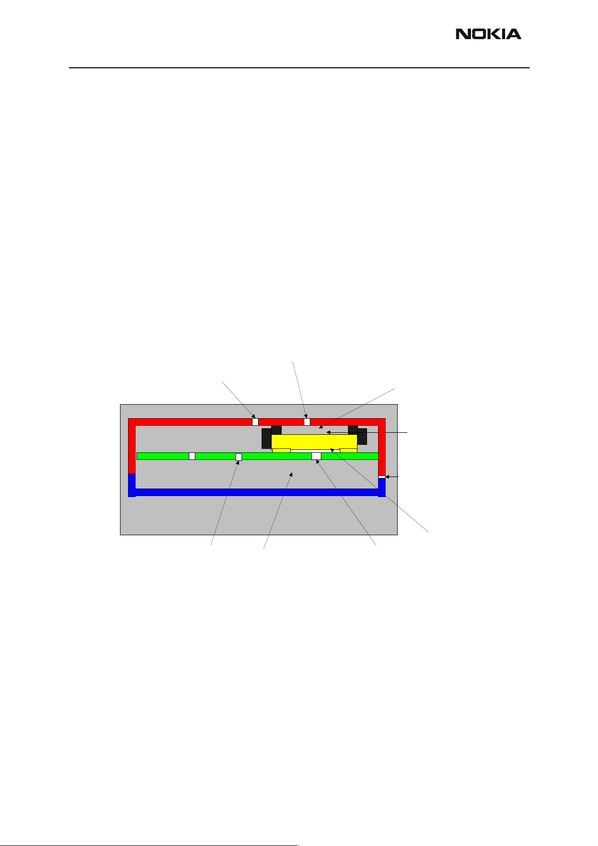
Figure 1 Audio block diagram ................................................................................................. 5
Figure 2 Sketch of earpiece acoustic design ....................................................................... 10
Figure 3 Mechanical assembly of earpiece and vibra ....................................................... 11
Figure 4 Earpiece frequency response - ERP corrected - non DSP corrected ............ 11
Figure 5 DAI receiving frequency response, B4.0 .............................................................. 12
Figure 6 Internal earpiece electrical interface ................................................................... 12
Figure 7 Microphone acoustical design ............................................................................... 14
Figure 8 DAI sending frequency response, B4.0 ................................................................. 14
Figure 9 Internal microphone electrical interface ............................................................ 15
Page 3-2 ãNokia Corporation. Original
Page 3

NPE-4
PAMS Technical Documentation 3 - Audio System
Description Page No.
List of Figures (continued)
Figure 10 Sketch of buzzer acoustic design .......................................................................... 17
Figure 11 Mechanical buzzer asssembly ................................................................................ 17
Figure 12 Typical buzzer frequency response ....................................................................... 17
Figure 13 Buzzer driver circuit .................................................................................................. 18
Figure 14 Vibra driver circuit ..................................................................................................... 19
Figure 15 External microphone interface .............................................................................. 24
Figure 16 External earpiece interface ..................................................................................... 26
Figure 17 Sysyem connector - mechanical outline ............................................................. 28
Figure 18 Carkit audio interface. block diagram .................................................................. 32
List of Tables
Table 1 Parts list ....................................................................................................................... 6
Table 2 Supply voltages .......................................................................................................... 7
Table 3 Possible UEM gains for each input and output ................................................. 8
Table 4 Total UEM gain for each input and output in different audio paths ........... 8
Table 5 UEM ear output specification ................................................................................ 13
Table 6 Microphone input specifications ........................................................................... 16
Table 7 Buzzer driver specifications .................................................................................... 18
Table 8 Vibra driver specifications ....................................................................................... 20
Table 9 Vibra output frequency control ............................................................................. 20
Table 10 HDC-9P interface specifications ........................................................................... 21
Table 11 Selected specifications for HDW-1 BT headset ................................................. 21
Table 12 LPS-1 interface specifications ............................................................................... 22
Table 13 Microphone input specifications, external audio ............................................. 25
Table 14 UEM HF output specifications ............................................................................... 26
Table 15 System connector pin assignment ........................................................................ 28
Table 16 HEADINT voltage value table used for accessory identification ................... 30
Original ãNokia Corporation. Page 3-3
Page 4

NPE-4
3 - Audio System PAMS Technical Documentation
Introduction
This Chapter specifies the Audio hardware for the NPE-4 program.
Abbreviations
UEM Universal Energy Management
UPP Universal Phone Processor
UIF codec User InterFace Codec in UPP
VBAT Main battery voltage
PWM Pulse Width Modulated (signal)
MUX MUltiPlexer
GND Phone ground
LGND GND abbreviation in System connector
SGND Signal ground – reference for microphone
MCU MicroController Unit
PWB Printed Wire Board
ERP Ear Reference Point
MRP Mouth Reference Point
SPL Sound Pressure Level (reference value 20 uPa)
BT BlueTooth
AGC Adaptive Gain Control
DRC Dynamic Range Compressor
ALWE Noise suppressor algorithm
AEC Acoustic Echo Canseler
IMD Insert Moulded Decoration
SCO Syncronous Connection Oriented
LPRF Low Power Radio Frequency (BlueTooth)
PWM Pulse Width Modulated
Page 3-4 ãNokia Corporation. Original
Page 5
NPE-4
PAMS Technical Documentation 3 - Audio System
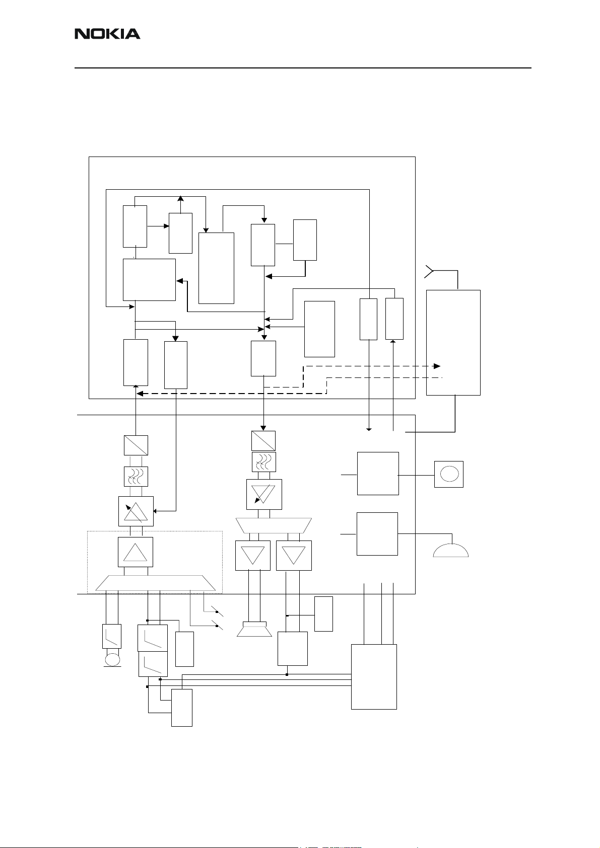
Technical overview
Block Diagram
VAD
U-ALWE /
UDRC
Encoder
Decoder
VAD
D-ALWE /
DRC
UPP
UEM
AEC
Mic Equaliser
MICDATA
D
A
0-22.5dB
filter
Anti-alias
0 / 20 dB
MUX
AGC
Speech codec
Sidetone
SC DAC
Ear
Equaliser
EARDATA
A
D
6 dB
-30 - 0dB
MUX
Tone Generator
6 dB
PWM
PWM
DAI4 Mic
FBUS Tx
Vibra Driver
Buzzer Driver
DAI4 Ear
FBUS Rx
SCO Airlink
BT102
LPRF
CBUS
VIBRA
M
BUZZO
Figure 1. Audio Block diagram
HF
Boomer
+8.2 dB
HFCM
HookInt
MBUS
FBUS Tx
FBUS Rx
CARK-91
MIC1P
HP 1
MIC
MIC1N
MIC2P
MIC2N
HP 3
HP 2
MIC3N
MIC3P
HeadInt
LOOPSET
HEADSET /
EARP
EARPIECE
EARN
Original ãNokia Corporation. Page 3-5
Page 6
NPE-4
3 - Audio System PAMS Technical Documentation
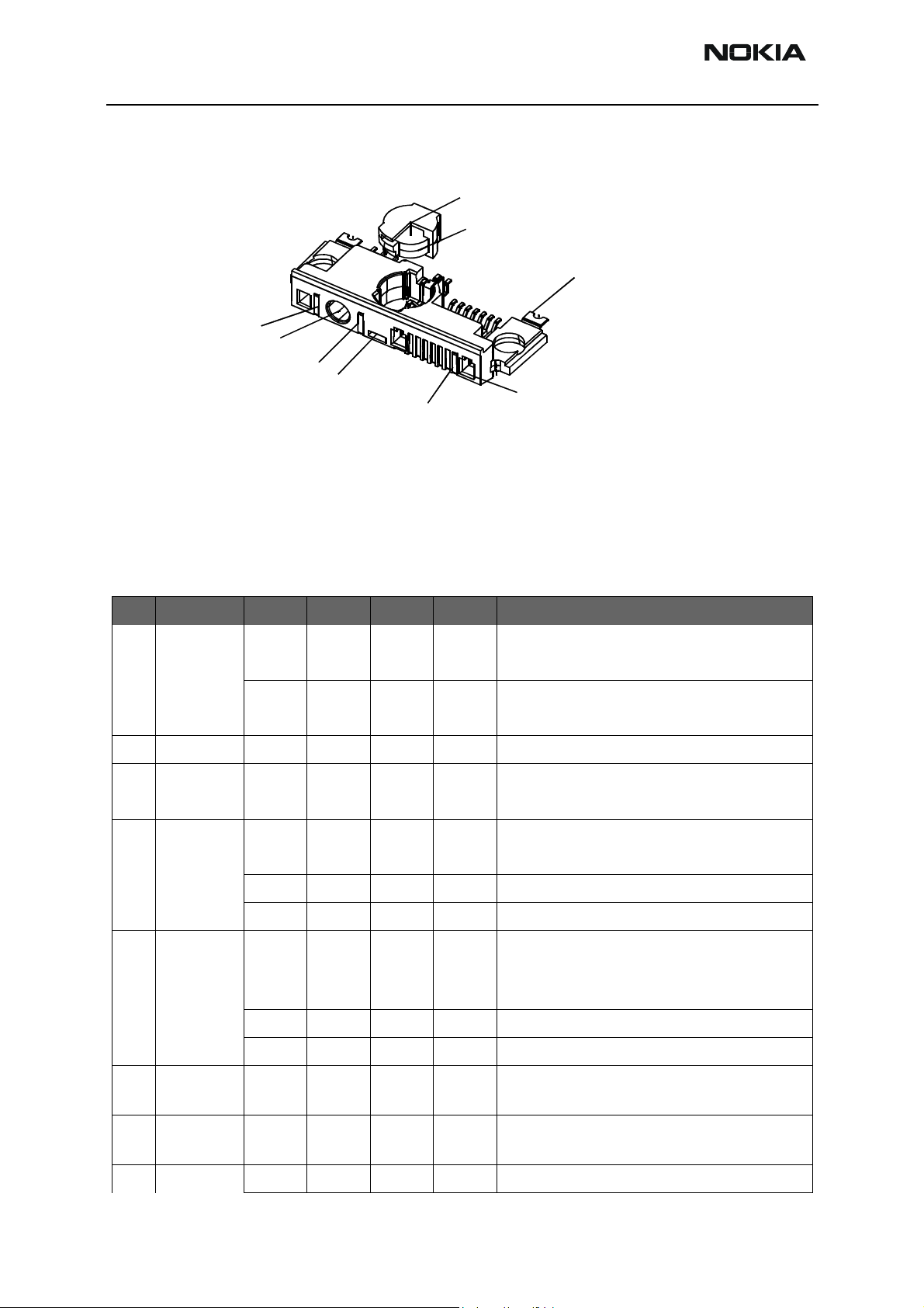
Part List
All involved key parts are listed in the following table. As seen in the table there is only
one vendor for some of the audio and vibration key components.
Table 1: Parts list
NAME OF THE
SUB-MODULE
Buzzer 1 MCC-03ACS STAR 5140209
Earpiece 2 TYPE: WD 00518/32 U
Earpiece 1 LT 201 KIRK Acoustics 5140233
Microphone assy 1 WM-64-HNY-310 MATSUSHITA 5140225
Vibrator 1 KHN4NB1H MATSUSHITA 6800043
Headset HDC 9P NMP
Loopset LPS-1 NMP
Carkit
- Handsfree unit
- Handsfree earpiece
- Microphone
- Handset unit
COMPONENT
DESIGNATION
CODE: 2403 252 08108
CARK-91
- HFU-2
- HFS-12
- HFM-8
- HSU-1
VENDOR
MATERIAL
CODE
PHILIPS Earpiece Systems 5140067
NMP
Bluuetooth Carkit
- Junction box
- Remote control button
- Handsfree earpiece
- Microphone
- Handset unit
Bluetooth headset HDW-1 NMP 0694064
UEM 4370805
UPP 4370815
Boomer LM4890 National semiconductors 4341221
System connector 5469061
CARK-112
- HFW-1
- CUW-2
- HFS-12
- HFM-8
- HSU-1
NMP 0750135
Page 3-6 ãNokia Corporation. Original
Page 7
NPE-4
PAMS Technical Documentation 3 - Audio System
DC Characteristics
The audio relevant supply voltages are shown in the following table:
Table 2:
Line
Symbol
Vana 2.7 2.78 2.86 V (Mic bias buffer)
VBAT 3.1 (SW)
Vflash1 2.7 2.78 2.86 V (DLR3, HEADINT and HOOKINT pull
Vflash2 2.7 2.78 2.86 V (DLR3)
VIO 1.72 1.8 1.88 V (HOOKINT level shifter)
Minimum TYP. /
Nominal
0,005 80 mA Min. due to regulator stability
3.6 5.1 (SW)
(2.9 (HW))
0.005 70 mA Min. due to regulator stability
0.005 1.5 mA Sleep
0.005 40 mA Min. due to regulator stability
Maximum Unit Notes
(5.4 (HW))
Supply Voltages
V (Buzzer and Vibra driver). Min and
max due to SW cut off.
up)
Audio Function Description
Audio control
The audio control and processing is done by the UEM, which contains the audio codec
and the UPP contains DSP blocks, handling and processing the audio data signals.
The audio block diagram is presented in , page .
The UEM supports three microphone inputs and two earphone outputs. The inputs can be
taken from an internal microphone, a headset microphone or a handsfree-unit / Carkit
microphone. The microphone signals from different sources are connected to separate
inputs at the UEM ASIC. Inputs for the microphone signals are differential type.
MIC1 and EAR in/output are used for the internal microphone input and Earpiece output.
The Headset or handsfree unit / Carkit audio is connected to the MIC2 input / HF (single
ended) output. The MIC3/XEAR is connected to GND and not used in the NPE-4 project.
Input and output selection and gain control is performed inside the UEM ASIC (register
AudioCtrl (Gain and routing) and MicBias (microphone bias selection).
Additional gain is added in the DSP SW. This gain is controled by adaptive algorithms
(AGC, DRC, ALWE and AEC) and set as a function of background noise, signal level and
Original ãNokia Corporation. Page 3-7
Page 8
NPE-4
3 - Audio System PAMS Technical Documentation
echo canceling.
In case of BT audio the BT accessory and the phone is connected by both an ACL and SCO
air link. ACL is used for connection commands and SCO for the actual audio transmission.
In both cases the BT module (in accessory and phone) receives the audio signal. In the
phone this signal is routed from BT module over LPRF to DSP where it follows the regular
audio path through out the rest of the system. The BT module and MCU is connected by
the CBUS for exchanging low level information.
All BT Gain adjustments are done in the accessory. DSP tuning is done in UPP, completely
as usually.
Gain Table
The possible gain for each input and output is shown in The gain settings are controlled
in the 16 bit AudioCtrlR register. Note * MIC3 only used for test purposes in NPE-4.. Table
4: Total UEM gain for each input and output in different audio paths (modes). contains
the total gain for each input and output in different audio modes.
The gain settings are controlled in the 16 bit AudioCtrlR register.
Table 3:
UEM Pins Gain (dB)
Input / Output Programmable Fixed UEM To ta l
MIC1 0 to 22.5, step 1.5dB 20 20 to 42.5, step 1.5dB
MIC2 0 to 22.5, step 1.5dB 0 or 20 0 to 22.5 or 20 to 42.5, step 1.5dB
MIC3* 0 to 22.5, step 1.5dB 0 or 20 0 to 22.5 or 20 to 42.5, step 1.5dB
HF (single ended) -30 to 0, step 2dB 6 -24 to 6, step 2dB
EAR -30 to 0, step 2dB 6 -24 to 6, step 2dB
Possible UEM gains for each input and output
Note * MIC3 only used for test purposes in NPE-4.
Table 4: Total UEM gain for each input and output in different audio paths (modes)
Gain Table Normal Mode - Gain dB
UEM Signals ¯Handportable Headset Handsfree (Carkit)
INPUTS MIC1 20 to 42.5, step 1.5dB
MIC2 20 to 42.5 step 1.5dB 0 to 22,5 step 1.5dB
MIC3
OUTPUTS EAR -24 to 6, step 2dB
HF -24 to 6, step 2dB -24 to 6, step 2dB
Page 3-8 ãNokia Corporation. Original
Page 9

NPE-4
PAMS Technical Documentation 3 - Audio System
Deviations in gain performance:
Transmit gain absolute accuracy: -1.0 / 0.0 dB
Transmit gain variation (temperature, supply): +/- 0,7 dB
Transmit gain variation with frequency (300 – 3000 Hz): +/- 0,5 dB
Transmit gain variation with signal level (> -50 dBm0): +/- 0,5 dB
(<-50 dBm0: +/- 1.2 dB)
Receive gain absolute accuracy: +/- 0,5 dB
Receive gain variation (temperature, supply): +/- 0,7 dB
Receive gain variation with frequency (100 – 3000 Hz): +/- 0,5 dB
Receive gain variation with signal level (> -50 dBm0): +/- 0,5 dB
(<-50 dBm0: +/- 1.2 dB)
DSP Gain:
Initially the DSP gain uplink (Mic) is set to 12 dB and 0 dB downlink. This is done in the
Equaliser.
The AGC controled by the DSP is able to reduce the Uplink gain in the UEM by 18 dB
maximum in steps of 1.5 dB.
The DRC can either attenuate the signal or enhance in it in DSP by up to 10 dB.
Note: Local mode gains are uptimised for production testing and are not the same as in
normal mode.
Internal Audio Devices
NPE-4’s internal audio design is described in the following sections.
Earpiece
Receiver solution is selected to be a Kirk Acoustic earpiece. Earpiece design is leak tolerant with a front protection cover directly on the earpiece component. The Earpiece will
be placed in a moulded rubber gasket which seals the front cavity to the IMD Window.
In front of the earpiece and leakholes a shielding material will be placed to prevent dust
particles to migrate onto the earpiece diaphragm. This material consists of a grid material type Saati PES 120/41 from Tradex (It is the same material as in Nokia 8210).
The earpiece is designed to be approved in type approval by type 3.2, low leak artificial
ear (Ear Simulator Type 4195, Low Leakage). No support for type 1 artificial ear is made
(Ear Simulator Type 4185).
Original ãNokia Corporation. Page 3-9
Page 10
NPE-4
3 - Audio System PAMS Technical Documentation
Earpiece Acoustic Design
The earpiece is sealed to the front cover (IMD window) with a rubber gasket. The gasket
is fixed inside the A-cover by the vibra motor assembly.
The Earpiece and gasket is designed to seal perfectly against the front cover. There is no
well defined leakage as known from the NPE-3 project. This is done to have a better performance in the frequency area from 2 – 3.4 kHz and to prevent the possibility of an
acoustic feedback loop inside the phone mechanics.
There is no sealing between the earpiece and the PWB.
There are also holes through the PWB to make the design more leak tolerant by using the
volume between PWB and the B-cover.
A-Cover or window contains front and leakage holes. On the inside of the A-cover a dust
shield is placed. This shield covers both front and leakage holes.
Front Holes on A-Cover
Leakage Holes on A_Cover
Shielding material glued to A cover or IMD Window
Leakage Holes on PCB
Back Volume
Leakage Holes on PCB
Figure 2. Sketch of Earpiece Acoustic Design
Earpiece Front Volume
Leakage Between A_ and B_Covers
(Not well defined)
Opening Between
Earpiece and PCB
Page 3-10 ãNokia Corporation. Original
Page 11
NPE-4
PAMS Technical Documentation 3 - Audio System
Figure 3. Mechanical assemply of Earpiece and Vibra
Specified frequency response curve for the NPE-4 design (mechanics and Audio):
30
20
10
0
-10
SPL Response [dBPa]
-20
-30
100 1000 10000
Frequency [Hz]
Typical Response Upper Limit Lower limit
Figure 4. Earpiece frequency response - ERP corrected – non DSP corrected
Original ãNokia Corporation. Page 3-11
Page 12
NPE-4
3 - Audio System PAMS Technical Documentation
Absolute Sensitivity (Low leak): 26 dBPa/V ±3dB @ 1kHz. (0 dB on Figure 4. Earpiece frequency
response - ERP corrected – non DSP corrected)
Figure 5. DAI receiving frequency response, B4.0
Earpiece Electrical Interface
Earpiece circuit includes pads for earpiece together with 2 ferrite beads (Common mode
filter), 2 capacitors (900 MHz cut-off filter) and two varistors for ESD protection placed
near the Earpiece.
The low impedance, dynamic type earphone is connected to the differential output (EAR)
in the UEM audio CODEC. On the differential output 2 * 22 Ohm (R171) is placed for
noise reduction and to compensate for the high capacitance of the varistors (1 nF),
which could lead to instability in the UEM.
AUDIO(4:0)
Figure 6. Internal Earpiece Electrical Interface
Page 3-12 ãNokia Corporation. Original
Page 13
NPE-4
PAMS Technical Documentation 3 - Audio System
Ear output specifications from the UEM specifications:
Table 5: UEM Ear output specification
Parameter Te s t c o n d i t i o n Min Typ Max Units
Output swing @ 0dBm0,
GR=-6 dB
Output voltage swing With 60 dB signal to total
Output resistance PDM data with 50 % pulse
Load capacitance EARP to EARN 50 nF
Load resistance EARP to EARN 26 32
Load capacitance EARP to GND 200 pF
Differential offset voltage -50 50 mV
Common voltage level for
EAR output (EARP & EARN)
V
ASwing
distortion ratio
ratio in the DAC input
VCM
EAR
2.36 2.5 V
4.0 V
1.0
1.3 1.35 1.42 V
Microphone
An omni directional microphone (DCT3 type) is used. The microphone is placed in the
system connector sealed in its rubber gasket. The sound port is provided in the system
connector.
pp
pp
W
W
The microphone is delivered from Matsushita with the microphone mounted in the rubber gasket.
A new rubber boot (Microphone gasket) with a harder shore (shore 80 versus shore 50)
will be used, to increase production ease and subsequently the production yield.
The microphone is connected to the differential input (MIC 1) of the UEM.
Original ãNokia Corporation. Page 3-13
Page 14

NPE-4
3 - Audio System PAMS Technical Documentation
Sketch of Microphone Acoustic Design
Systemconector sound outlet
Rubber Gasket Volume
Figure 7. Microphone Acoustical Design
Mic
Absolute Sensitivity: -42 dBV/Pa ±3dB @ 1kHz.
System
connector
Connection
springs
Figure 8. DAI Sending frequency response, B4.0
The desired microphone response is a flat line in 0 dB between 300 Hz and 4 kHz that
roles off as much as possibly outside these frequencies.
Since the microphone response is flat, no DSP equalisation is found necessary.
Page 3-14 ãNokia Corporation. Original
Page 15

NPE-4
PAMS Technical Documentation 3 - Audio System
Microphone Electrical Interface
The microphone electrical circuit includes 2 ferrite beads for common mode noise rejection together with 2 capacitors for filtering the 900 MHz signal and two varistors for
ESD protection placed near the microphone PWB spring pads.
The 10 nF (C155) forms a low pas filter together with the microphone impedance to
make a steeper role off at high frequencies.
Also an extra High pass filter (R152 + C154) is added to limit audible TDMA-noise (217
Hz + harmonics) and to limit the bumpy road noise.
A transistor circuit (V150) on the bias line from UEM is used as the voltage supplier for
minimising the noise level from the UEM bias output.
This gives an decrease in the DC voltage level across the Microphone to typically 1.1 V
(1.3 V re. GND). Using Matsushita microphones as single supplier this will not pose any
problems as the FET in the microphone have little variation on their Vds curves.
The Microphone bias is controlled in the 8 bit AudioBiasR register. The 1 uF (C171) is lessons learned from NPE-3 and simulations shows that this will give an even higher noise
suppression. But it has the risk of oscillating. No difference has been measured on preliminary tests.
AUDIO(4:0)
Figure 9. Internal Microphone Electrical Interface
Original ãNokia Corporation. Page 3-15
Page 16

NPE-4
3 - Audio System PAMS Technical Documentation
UEM microphone input specification:
Table 6: Microphone input specifications
Parameter Symbol Min Typ Max Unit
Microphone amplifier input resistor R
Differential input voltage range for MIC1
input, G =20 dB
Receive Common mode input voltage
range for MIC input
Common mode voltage level V
Differential mode voltage range for
microphone amplifier, at gain = 20dB
Differential load resistance for the
microphone input stage
Transmit gain absolute accuracy GXA -1.0 0.0 dB
Transmit gain variation with programmed
gain, temperature and supply
Common mode rejection ratio CMRR 45 60 dB
M30
V
IN1
V
HFCM
CM
V
OUT
R
OS
GXAGT
V
30 50 kOhm
200 1200 m V
100 m V
1.3 1.35 1.4 V
2.0 V
30 450 kOhm
-0.7 0.7 dB
PP
PP
PP
Buzzer
Alerting tones and/or melodies are generated by a buzzer, which is controlled by a PWM
signal from the UEM. The SPL requirement is to be as good or better than the NPE-3 in
comparison test. The buzzer is delivered from the supplier with an end of line requirement of 102dB (A) at 5cm and 2.5 kHz.
The actual level is found from a comparison with NPE-3 on specific ringing tones.
The buzzer is designed to have the first resonant peak at 2500 Hz. The ringer melodies
will be optimised in DSP so the main frequency of any given melody is shifted to near the
resonant peak. For this optimisation a program called BuzzCalc will be used for the calculation of the dominating frequency of a given ringing melody or tone.
The design of the buzzer is a direct copy from the NPE-3 project. The Buzzer is glued to a
gasket. This final assembly is delivered by STAR. Sound holes are placed in the A-cover
The A-cover is designed to give an optimal SPL by securing the tightness between buzzer
and A-cover.
The buzzer is electrically connected to the PWB by spring contacts.
Page 3-16 ãNokia Corporation. Original
Page 17

NPE-4
PAMS Technical Documentation 3 - Audio System
Buzzer Acoustic Design
Buzzer Resonance
Chamber Volume
Buzzer
Sound Port
Spring Contacts
PCB
Figure 10. Sketch of Buzzer Acoustic Design
The important parameters in this design are the front cavity and the sound portholes.
A-Cover
Rubber
gasket
Figure 11. Mechanical buzzer assemply
The expected A weighted frequency response is (50 % Duty cycle). Tested in a simplified
testbox. Final result expected to lay 2-4 dB below.
Buzzer frequency response
108
106
104
102
100
98
96
SPL / dB(A)
94
92
90
88
0 1000 2000 3000 4000 5000 6000 7000
Freq. / Hz
Figure 12. Typical buzzer frequency response
Original ãNokia Corporation. Page 3-17
Page 18

NPE-4
3 - Audio System PAMS Technical Documentation
Buzzer Electric Interface
The driver circuit is an integral part of the UEM.
UEM
5kOhm
+/- 35%
BUZZPWM
Figure 13. Buzzer driver circuit.
Table 7:
Parameter Variable Min Ty p Max Unit
Output switch resistance Rbuzzo 1.0 2.7 4.5 Ohm
Buzzer driver specifications
VBATDriv
BUZZO
VSADriv2
VBAT
1 uF
BUZZER
12 pF
Output peak sink current Iout VBAT 120 180 350 mA
Output peak sink voltage Uout VBAT 0.5 1.2 V
Output pwm duty cycle Pdcyc 50 %
Buzzer coil resistance Rload 13 16 19 Ohm
Battery voltage VBAT Ni or Li battery 3.03 3.6 5.2 (Ni)
4.2 (Li)
Reverse diode peak current Iforw tp = 10 us 0.35 A
Output frequency Fout, GSM system 0.48 2500 7751 Hz
V
The buzzer is controlled from the UEM by a PWM (Pulse Width Modulated) square wave
signal.
The frequency is produced by a bitstream on register BUZZFREQR that is counted
through a 21 bit accumulator:
BuzzClkout
21
)1)/2/((
+= BuzzFreqRFF
BuzzClk has the same frequency as the CBusClk (1 MHz for GSM).
Page 3-18 ãNokia Corporation. Original
Page 19

NPE-4
PAMS Technical Documentation 3 - Audio System
When buzzer DigEna = 1 then a PWM signal is present at BUZZPWM
The buzzer duty cycle is defined by:
%78125.0*)0:5(Cycle BPWMDCRDuty =
Vibra specification
A vibra alerting device is used to generate a vibration signal for an incoming call. The
vibra is placed in the top of the phone. It is fastened to the A-cover by means of a rubber
gasket and a lid which are pressed into the A-cover see .
The vibra is electrically connected to the PWB by spring contacts.
The vibra is controlled from the UEM by a PWM (Pulse Width Modulated) square wave
signal.
Vibrator Electrical Interface
The driver circuit is an integral part of the UEM.
The two 33 nH inductors are added for decoupling the vibra motor from the RF antenna
field. The two 1 nF capacitors are placed for ESD purposes.
UEM
Vibraclk
Vibra electrical specifications
VBATDriv
5kOhm
+/- 35%
VIBRA
VSADriv2
Figure 14. Vibra driver circuit
1 uF
33nH 33nH
10 nF
VBAT
Vibra
M
1 nF
Operating voltage = 1.0 V – 1.2 VDC (Controlled by the Duty cycle)
Starting Current = max 140 mA
Starting voltage = max 1 VDC
Terminal Resistance = 8.8 Ohm (typical)
Coil = 40 uH (typical)
Typical rpm: 9000 at 1.1 VDC.
Original ãNokia Corporation. Page 3-19
Page 20

NPE-4
3 - Audio System PAMS Technical Documentation
Table 8:
Parameter Variable Min Typ Max Unit
Output swhich resistance Rvibra 1.4 4.2 7.5 Ohm
Output average current Ivibra VBAT 50 80 135 mA
Output peak current Ipeak VBAT 300 mA
Output frequency Fvibra 64 129 520 Hz
Output duty cycle Dvibra 2.9 47 96.9 %
Reverse diode peak current Iforw tp = 10 us 0.30 A
Motor average dc Udc_motor VBAT=3.0 ... 4.5 V 1.0 1.5 2.3 Vdc
Output current high imp Ihiz V_ANA, VBAT -1 1 uA
Vibra driver specifications
Valid frequencies are: 64, 129, 258 and 520 Hz
The duty cycle of the vibra output is selected by the VCLKR register bit #7 .. #4. This is 16
accumulated duty cycles from 2.9 % to 96.9 %
The frequency of the vibra is selected by the VCLKR register bit #D1 and #D0, this clock
is divided down from the 32.768 Hz clock.
Table 9: Vibra output frequency control
D1 D0 Vibra output frequency
0 0 64,1
0 1 128,5
1 0 258,0
1 1 520,1
External Audio Devices
Audio Accessories
NPE-4 is supporting the following DCT3 and bluetooth audio accessories:
Headsets:
HDC-9P
Headset is the simplest audio accessory to use. It merely only consists of an earpiece, a
microphone, and a swhich which in technical terms is often referred to as a HOOKswhich or Headset button. The HOOK-swhich can be used either to answer in-coming
calls, to end a call or to initiate voice dialling calls.
The Hook interrupt is detected by software polling on the UEM hookInt input pin
Page 3-20 ãNokia Corporation. Original
Page 21
NPE-4
PAMS Technical Documentation 3 - Audio System
HDC-9P is a purely passive audio accessory.
HDW-1
Table 10:
Object Specification Notes
Receiver input impedance 150 Ohm +/- 25 % @ 390 mV at 1 kHz
Maximum Sound pressure level 106 dB SPL at 1 mW
Transmitter output impedance 2200 Ohm +/- 30 % at 1 kHz
Transmitter sensitivity - 43.5 dBV/Pa +/- 3 dB at 1 kHz
XMIC bias voltage 1.5 V Typical
XMIC bias current 1.5 mA Maximum
HDC-9P interface specifications
Bluetooth headset developed in the Tomahawk project.
The BT headset is containing a microphone, a earpiece, bluetooth module and its own
audio codec. HDW-1 is battery supplied
Audio connection is full duplex digital transmission with error correction.
Table 11: Selected specifications for HDW-1 BT Headset
Min Typ Max Unit
Ear signal in Codec after PCM
DAC converter
Ear signal amplifier gain in codec -18 2 12 dB / setting by 2 dB steps
Electroacoustic transfer function
(Rx)
Microphone signal level 3 4 6 mV/Pa
Level at AD input in Codec 58 490 mVrms in codec
Mic. amplifier gain in codec 20 42.5 dB
Noise voltage, microphone 5 uVrms
80 490 mVrms in codec
17 dBPa/V/0.5m
Loopsets:
LPS-1
The Loopset is a hearing aid accessory for hearing impaired persons to use mobile
phones.
It consists of a Wire-loop and a microphone placed in a collar around the person's neck.
This is detected in the mobile as a Headset. In the UI SW it is possible to change profile
Original ãNokia Corporation. Page 3-21
Page 22

NPE-4
3 - Audio System PAMS Technical Documentation
from Headset to Loopset enabling the use of Loopset specific DSP tunings.
The coil amplifier is supplied from MICB2 bias voltage.
No voice dialling from the accessory is possible while there is no hookswhich (voice dialing have to be activated from the phone keypad).
Table 12: LPS-1 interface specifications
Object Specification Notes
Receiver input impedance 100k Ohm +/- 5 % Magnetic loop
Transmitter output impedance 1600 Ohm +/- 30 % at 1 kHz
XMIC bias voltage 1.3 V Maximum
XMIC bias current 400 uA Maximum
Carkits:
CARK-91
The carkit consists of the following components:
MCC-1: Active handset holder with connection for the HFU-2 to mobile
HFU-2: Handsfree unit incl. fast charger, HF – microphone and earpiece amplifiers, interface to handset, datacard and phone and control circuit
HHS-9: Swivel mount
PCH-4J: Mounting cable
HFS-12: Handsfree earpiece, permanently installed in the car.
HFM-8: External handsfree microphone. HFM-8 is an option for the user to have a
separate microphone for the carkit-installation. HFM-8 is designed to be permanently
installed in a car.
The internal microphone in the mobile is muted by a MBUS message from
the HFU-2 when the external microphone is detected in HFU-2.
No data call is possible in HFU-2 while DAU-9 datacable is not supported.
External accessory for Cark-91:
HSU-1: Handset unit with hookswhich. This is a handset used for private conversations without losing the link to the external antenna.
Page 3-22 ãNokia Corporation. Original
Page 23

NPE-4
PAMS Technical Documentation 3 - Audio System
Carkit - 112
The carkit consists of the following components
HFW-1 Bluetooth junctionbox which replaces HFU-2 in the Cark-91 setup
CUW-2 Remote control Button, earpiece volume and hookswhich
And all the components mentioned in Carkit-91 apart from HFU-2 and HSU-1.
Bluetooth carkit developed in the Tomahawk project.
External Audio Interface
The interface is basically a 3-wire solution, which gives two completely separate audiopaths, microphone- and earpiece-signals. The interface is split up into:
External earpiece: XEAR (external earpiece, single ended)
External microphone: XMICP (ex
XMICN (external microphone, negative)
ternal microphone, positive)
External Audio Interface — Electrical Interface
The external audio connections are presented in Figure 15. External Microphone Interface and The hookInt is pulled up by 47 kOhm and the detection is being polled by software on GENIO2 via the Inverter circuit. A 100k Ohm resistor is added to the Hookint line
to avoid DC-clicks in the Uplink path.. A headset or a handsfree unit can be connected
directly to the system connector. The headset microphone bias is supplied from UEM
MICB2 output and fed to the microphone through XMICP line.
Note: MIC3 lines will be disconected from MIC2 and grounded near the UEM.
Original ãNokia Corporation. Page 3-23
Page 24

NPE-4
3 - Audio System PAMS Technical Documentation
XAUDIO(11:0)
GENIO(0)
Figure 15. External Microphone Interface
See Table 13. Microphone input specifications, external audio for the input specifications
for the external microphone.
The external audio interface microphone electrically circuit includes 2 ferrite beads for
common mode rejection together with 2 capacitors for filtering the 900 MHz signal.
An extra Lowpass filter (R167 and C172) for a steeper role-off at higher frequencies and
two high pass filters (C165 and R166 (- 3dB: 234Hz), C164 and R165 (- 3dB: 102Hz)) are
added to limit the audible TDMA-noise and to improve bumpy road noise suppression.
A transistor circuit on the bias line from UEM is used for a voltage supplier for minimising the noise level from the UEM bias output.
The Microphone bias is controlled in the 8 bit AudioBiasR register.
When DLR-3 cable is not connected there is a 330 Ohm pulldown resistor from SGND
(XMICN) to L-GND (R172). When DLR-3 is connected Vflash2 voltage of 2.78 V is used as
supply for the data cable on SGND line.
Page 3-24 ãNokia Corporation. Original
Page 25

NPE-4
PAMS Technical Documentation 3 - Audio System
Connections for MIC3 are grounded near the UEM and not as shown in Figure 15. External Microphone Interface connected to MIC2 lines.
Table 13: Microphone input specifications, external audio
Parameter Symbol Min Typ Max Unit
Microphone amplifier gain for MIC 2 / Handsfree MicG2 0 22,5 dB
Microphone amplifier gain for MIC 2 / Headset MicG2 22.5 42,5 dB
Microphone amplifier input resistor R
Differential input voltage range for MIC2 input,
G =20 dB
Differential input voltage range for MIC2 input,
G =0 dB
Receive Common mode input voltage range for
MIC input
Common mode voltage level V
Differential mode voltage range for microphone
amplifier, gain 20 dB
Differential load resistance for the microphone
input stage
Transmit gain absolute accuracy GXA -1.0 0.0 dB
Transmit gain variation with programmed gain,
temperature and supply
Common mode rejection ratio CMRR 45 60 dB
MIC
V
IN2
V
IN2
V
INCMR
CM
V
OUT
R
GS
GXAGTV -0.7 0.7 dB
30 50 kOhm
200 m V
2.0 V
100 m V
1.3 1.35 1.4 V
2.0 m V
30 450 kOhm
PP
PP
PP
PP
From the UEM output a Boomer circuit is added to give enough output swing to the
headset. The boomer is coupled as differential input single ended output. The differntial
input is using HF / HFCM output from the UEM.
The Boomer is controled by UPP GENIO14. This control signal enables and disables the
boomer wich have a internal circuit for uptimal and clickfree startup.
The boomer timing is mostly controled by C176. The nearly clickless operation has been
made by timing in the MCU SW (A 12 msec delay between UEM and Bommer startup and
a 1 sec delay between boomer and UEM shutdown has be made.)
The Gain of the circuit is controled by R176 / R 180 and R177 / R 178. Leading to a
Boomer HW gain of approximately 3 dB.
Original ãNokia Corporation. Page 3-25
Page 26

NPE-4
3 - Audio System PAMS Technical Documentation
Filtering in the boomer circuit:
Highpass: -3dB point = 234 Hz
Lowpass: -3dB point = 3386 Hz
The 15 Ohm with a load of 150 Ohm reduce the output level with approximately 0.8 dB.
XEAR circuit includes 1 ferrite bead HF filter, 1 capacitor (900 MHz cut-off filter) and
one 10 nF capacitor (C?? (R161)) placed near the system connector for EMC purposes.
On the single ended output 15 Ohm (R183) is placed to compensate for the high capacitance of the 10 nF condensator, which could lead to instability in the Boomer.
The hookInt is pulled up by 47 kOhm and the detection is being polled by software on
GENIO2 via the Inverter circuit. A 100k Ohm resistor is added to the Hookint line to avoid
DC-clicks in the Uplink path.
10n
10n
UEMUPP
68k
68k
15
C?? (R161)
10n
GND
Figure 16. External Earpiece Interface
Table 14: UEM HF output specifications
Parameter Test condition Min Typ Max Unit
Output voltage swing
single ended mode
Output voltage swing fully
differential mode
Output resistance (0 Hz
to 4 kHz)
Parasitic load resistance HF to HFCM (with external audio
with 60 dB signal to total distortion
ratio
with 60 dB signal to total distortion
ratio
PDM Data with 50 % pulse ratio in
the DAC input
circuitry)
1.0 V
2.0 V
1 Ohm
10 nF
PP
PP
Load resistance HF to HFCM or VSA (with
30 45 Ohm
headset)
Page 3-26 ãNokia Corporation. Original
Page 27

NPE-4
PAMS Technical Documentation 3 - Audio System
Table 14: UEM HF output specifications
Parameter Test condition Min Typ Max Unit
Offset voltage -50 50 mV
Common voltage level for
HF output (HF and
HFCM)
Pull down resistor value in
HF output
Pull down swhich
resistance in HFCM
output
VCM
R
PD
R
SW
HF
0.75 0.8 0.85 V
3 10 25 kOhm
400 Ohm
HEADINT and HOOKINT are ‘interrupts input’ in UEM.
Headint is used to identify the type of accessory that is connected to the system connector. The interrupt is generated by pulldown resistors in the respective accessories.
Hookint is used for detecting the hook swhich of the headset.
HF is the audio output through which audio can be routed to either Headset-earpiece or
Carkit earpiece. HF is wired as single ended output, which in reality performs the audioamplification.
MIC2P, MIC2N, MIC3P and MIC3N are all inputs to the microphone amplifier in the
UEM. In short form the main difference for the listed inputs are:
MIC2P, MIC2N: Rated to audio signals up to 2 Vpp (with gain 0 dB). Used for Headset
and Carkit microphone.
MIC3P, MIC3N: Rated to audio signals up to 2 Vpp (with gain 0 dB). Used for FM Radio
Both types of inputs can be wired and used to either fully differential or singled-ended
operation, however the fully differential configuration is chosen for the DCT3 interface.
External Audio Connector
The accessibility to the external audio interface is reached by the system connector.
Original ãNokia Corporation. Page 3-27
Page 28
NPE-4
2
4
3 - Audio System PAMS Technical Documentation
The configuration for the bottom connector is shown in the following figure.
Rubber boot
Microphone
3
8
13
Contact 1
DC-jack
2,3,4
Contact 5
Microphone port
Contacts
8...13
Contact 14
14
Figure 17. System connector – mechanical outline
External Audio Signal Electrical Specification
Table 15: System connector pin assignment
Pin Name Min Typ Max Unit Notes
1 VIN
0
0
0
8.5
850
16.9
1.0
V
mA
Vpeak
Apeak
Unloaded Fast Charger
Supply current
Unloaded Standard Charger
Supply current
Solderable element,
2 pcs
Cable/Cradle connector
guiding/fixing hole, 3 pcs
2 L-GND 0 0 0 V Supply ground DC Jack
3 VIN
4 CHRG_
CTRL
0
0
0
1.7
8.5
850
0.8
2.9
V
mA
V
Unloaded Fast Charger DC Jack
Supply current
Charger control (PWM) dig. Low DC Jack
Charger control (PWM) dig. High
1 32 37 Hz PWM frequency for a fast charger
1 99 % PWM duty cycle
5 CHRG_
CTRL
0
1.7
0.8
2.9
V
Charger control (PWM) dig. Low Bottom
charger contacts
Charger control (PWM) dig. High
1 32 37 Hz PWM frequency for a fast charger
1 99 % PWM duty cycle
6 MICP 0 2 100 mV Connected to UEM MIC1P input. (re.
SGND)
7 MICN 0 2 100 mV Connected to UEM MIC1N input. (re.
SGND)
8 XMIC 2.0 2.2 kW Input AC impedance
Page 3-28 ãNokia Corporation. Original
Page 29

NPE-4
PAMS Technical Documentation 3 - Audio System
Table 15: System connector pin assignment
Pin Name Min Typ Max Unit Notes
1 Vpp Maximum signal level
0 1.55 V Mute (output DC level)
2.5 2.9 V Unmute (output DC level)
100 600 µA Bias current from UEM
2 Vpp
9 SGND 330 W Resistance to phone ground, return path for
10 XEAR 47 W Output AC impedance (ref. LGND)
10 µF Series output capacitance
16 300 W Load AC impedance to GND (Headset) pin
4.7 10 kW Load AC impedance to GND (Accessory)
1.0 Vpp Maximum output level (no load)
6.8 kW Load DC resistance to GND (Accessory)
16 1500 W Load DC resistance to GND (Headset) pin
2.78 2.8 2.86 V DC voltage (47k pull-up to Vflash1)
Microphone signal (Gain 0 dB)
Connected to UEM MIC3P + MIC2P input
XMIC. When the DLR-3 datacable is
connected, SGND swhiches to be a supply
line for the cable (2.8V)
#14
pin #14
pin #14
#14
HEAR 0 14 220 mV
11 MBUS
12 FBUS_R
X
13 FBUS_TX
14 L-GND 0 0 V Supply ground
0
2.0
0
2.0
0.1
1.7
0.8
2.8
0.8
2.8
0.8
2.8
V Serial bi-directional control bus.
V Fbus receive. Serial Data
V Fbus transmit. Serial Data
Earphone signal
Connected to UEM HF output
Baud rate 9600 Bit/s
Phone has 4.7kW pull up resistor in UEM
Baud rate 9.6k-230.4kBit/s
Phone has 220kW pull down resistor
Baud rate 9.6k-230.4kBit/s
Phone has 47kW pull up resistor in UEM
Original ãNokia Corporation. Page 3-29
Page 30
NPE-4
3 - Audio System PAMS Technical Documentation
Accessory Detection, Identification and Control
Accessory Detection
Accessories are detected when the XMIC signal is loaded with either DLR3, Loopset or
Headset. The interrupt is generated by pulldown resistors in the respective accessories.
Carkit 91 is detected via communication on the MBUS line.
BT accessories are connected after BT connectivity is chosen in UI. Communication with
UEM is done over the CBUS lines.
Accessory Identification
The voltage on the XMICP is used to identify which type of accessories that are connected to the system connector. See Table 16: HEADINT Voltage Value Table used for
Accessory Identification. The HEADINT interrupt is detected in the UEM and this voltage
level is used to determine the type of accessory.
A voltage is measured on the HeadInt input on the UEM. This signal is multiplexed to an
A/D converter in the UEM. From this level an Accessory server recognises the type of
accessory and chooses the relevant audio accessory tuning if applicable. If the detection
voltage window is as described in Table 16: HEADINT Voltage Value Table used for Accessory Identification for headset and loopset the microphone bias is enabled.
If DLR3 is used the detection voltages are as in Table 16: HEADINT Voltage Value Table
used for Accessory Identification, no bias for the microphone is enabled and 2.8 V DC for
DLR3 is supplied.
Table 16: HEADINT Voltage Value Table used for Accessory Identification
ACCESSORY CONNECTED HEADINT
VOLTAGE LEVEL
MIN MAX
Headset HDC-9P and Loopset LPS-1 19 mV 300 mV Without MBias
Varying with microphone FET
working line.
Carkit CARK-91 Detected and acknowledged by the
phone on MBUS
NOTES
DLR3 300 mV 800 mV
Page 3-30 ãNokia Corporation. Original
Page 31

NPE-4
PAMS Technical Documentation 3 - Audio System
Accessory Control
Headset and Loopset
In the HDC-9P the headset-button is electrically connected across the XEAR and L-GND
lines. When the Headset button is activated, XEARP is short-circuited to L-GND and a
HOOKINT interrupt is detected in the UEM. This is used to lift the receiver, to put it down
or initiate voice call.
HDW-1 is a Bluetooth Headset. The BT headset is recognised by the phone after a BT
search for any BT component in the vicinity has been performed and a connection is set
up via the BT module in both phone and accessory.
In case of BT audio the BT accessory and the phone is connected by both an ACL and SCO
air link. ACL is used for connection commands and SCO for the actual audio transmission.
In both cases the BT module (in accessory and phone) receives the audio signal. In the
phone this signal is routed from BT module over LPRF to DSP where it follows the regular
audio path through out the rest of the system. The BT module and MCU is connected by
the CBUS for exchanging low level information.
Carkit
CARK-91
The carkit communicates with the phone through the system connector via the MBUS
lines. No interrupts are detected on the HeadInt or HookInt. Headint is disabled so a voltage on the XMIC line is not able to initiate the interrupt. All communication is controlled
in the HFU-2 unit. Voice dialling is only possible in CARK-91 via phone "name" softkey.
The HFU-2 sends an MBUS registration messages to the phone when the HFU-2 is powered up. This message includes an identification number for the HFU-2 box. The phone
will send an acknowledge message and communication are set-up.
The HFU-2 box includes power amplifier for Earpiece (nom. gain 26 dB) and preamplifier
for Microphone (nom. gain 30 dB).
Original ãNokia Corporation. Page 3-31
Page 32

NPE-4
3 - Audio System PAMS Technical Documentation
HFS-12
HFM-8
UEM
MBUS
HFU-2
26 dB
Audio
Interface
30 dB
External
audio sheet
System
connector
EMI Filter
System
connector
MCC-1
MBUS
Figure 18. Carkit audio interface. Block diagram.
Control
circuit
MBUS
MBUS
CARK-64
This carkit is a passive kit and is just a holder for the phone. No detection is done anywhere.
CARK-112
This is a Bluetooth carkit. The BT Carkit is recognised by the phone after a BT search for
any BT component in the vicinity has been performed and a connection is set up via the
BT module in both phone and accessory.
In case of BT audio the BT accessory and the phone is connected by both an ACL and SCO
air link. ACL is used for connection commands and SCO for the actual audio transmission.
In both cases the BT module (in accessory and phone) receives the audio signal. In the
phone this signal is routed from BT module over LPRF to DSP where it follows the regular
audio path through out the rest of the system. The BT module and MCU is connected by
the CBUS for exchanging low level information.
Voice dialling is only possible in CARK-112 via phone "name" softkey.
Page 3-32 ãNokia Corporation. Original
 Loading...