

Page 1

Programmes After Market Services
NPE-4 Series Cellular Phones
6 - Troubleshooting
Original ãNokia Corporation. Page 6-1
Page 2

NPE-4
6 - Troubleshooting PAMS Technical Documentation
Table of Contents
Page No.
Introduction ...................................................................................................................................... 5
Baseband Troubleshooting ..................................................................................................... 5
Phone is dead ..................................................................................................................... 5
Flash programming doesn’t work ................................................................................. 7
Power doesn’t stay on, or phone jammed .................................................................. 8
Display information: “Contact service” ....................................................................... 9
The phone doesn’t register to the network or phone doesn’t make a call ......... 11
SIM failure .......................................................................................................................... 11
Display failure .................................................................................................................... 13
Keypad failure .................................................................................................................... 14
Audio faults ........................................................................................................................ 17
Charger faults .................................................................................................................... 19
Blue Tooth module faults ................................................................................................ 20
RF Troubleshooting .................................................................................................................. 23
Introduction ........................................................................................................................ 23
RF Key component placement ................................................................................ 24
RF Measurement points ........................................................................................... 25
PA Can ................................................................................................................... 25
Hagar RF can ....................................................................................................... 26
Abbreviations in fault finding charts ................................................................... 27
RF in general ....................................................................................................................... 28
EGSM Receiver ................................................................................................................... 29
General instructions for EGSM RX troubleshooting ......................................... 29
Fault finding chart for EGSM receiver ................................................................. 31
EGSM signal path ...................................................................................................... 31
RX/TX Switch ....................................................................................................... 31
Front-end .............................................................................................................. 32
Hagar ..................................................................................................................... 32
PCN Receiver ...................................................................................................................... 32
General instructions for PCN RX troubleshooting ............................................ 32
Fault finding chart for PCN receiver ..................................................................... 34
PCN signal path .......................................................................................................... 35
RX/TX Switch ....................................................................................................... 35
Front-end .............................................................................................................. 35
Page 6-2 ãNokia Corporation. Original
Page 3

NPE-4
PAMS Technical Documentation 6 - Troubleshooting
Table of Contents
Page No.
Hagar ..................................................................................................................... 36
EGSM Transmitter ............................................................................................................. 36
General instructions for EGSM TX troubleshooting ......................................... 36
Path of the transmitted EGSM signal .................................................................. 38
Hagar ..................................................................................................................... 38
PA ............................................................................................................................ 38
RX/TX Switch ....................................................................................................... 38
Fault finding chart for EGSM transmitter ........................................................... 39
PCN Transmitter ................................................................................................................40
General instructions for PCN TX troubleshooting ............................................. 40
Path of the transmitted PCN signal ...................................................................... 41
Hagar ..................................................................................................................... 42
PA ............................................................................................................................ 42
RX/TX Switch ....................................................................................................... 42
Fault finding chart for PCN transmitter .............................................................. 43
Synthesiser .......................................................................................................................... 44
General instructions for Synthesiser troubleshooting ..................................... 44
26 MHz reference oscillator (VCTCXO) ................................................................ 45
VCO ................................................................................................................................ 46
Fault finding chart for PLL Synthesiser ................................................................ 46
PLL Blockdiagram ....................................................................................................... 47
Frequency lists ............................................................................................................ 48
EGSM ..................................................................................................................... 48
PCN ......................................................................................................................... 49
SMD Guidelines for PA ..................................................................................................... 50
Removal instructions ................................................................................................ 50
Attachment instructions .......................................................................................... 50
Phoenix tuning ................................................................................................................... 52
RF tuning after repairs ............................................................................................. 52
RX Calibration ............................................................................................................. 52
EGSM ..................................................................................................................... 52
PCN ......................................................................................................................... 54
RX Band Filter Response Compensation .............................................................. 56
EGSM ..................................................................................................................... 56
PCN ......................................................................................................................... 56
Original ãNokia Corporation. Page 6-3
Page 4

NPE-4
6 - Troubleshooting PAMS Technical Documentation
Table of Contents
Page No.
RX Channel Select Filter Calibration .................................................................... 60
RX AM Suppression ................................................................................................... 62
EGSM ..................................................................................................................... 62
PCN ......................................................................................................................... 63
TX Power tuning ......................................................................................................... 65
EGSM ..................................................................................................................... 65
PCN ......................................................................................................................... 67
TX I/Q Tuning ............................................................................................................... 69
EGSM ..................................................................................................................... 69
PCN ......................................................................................................................... 73
Page 6-4 ãNokia Corporation. Original
Page 5

NPE-4
PAMS Technical Documentation 6 - Troubleshooting
Introduction
This section is a summary of experiences the NPE-4 R&D team made during the development. It covers some errors or wrong configurations and their symptoms as well as
advice for problem solving. The section is seperated into two main parts the Baseband
troubleshooting and the RF troubleshooting, however, it is advisable to read both parts.
Baseband Troubleshooting
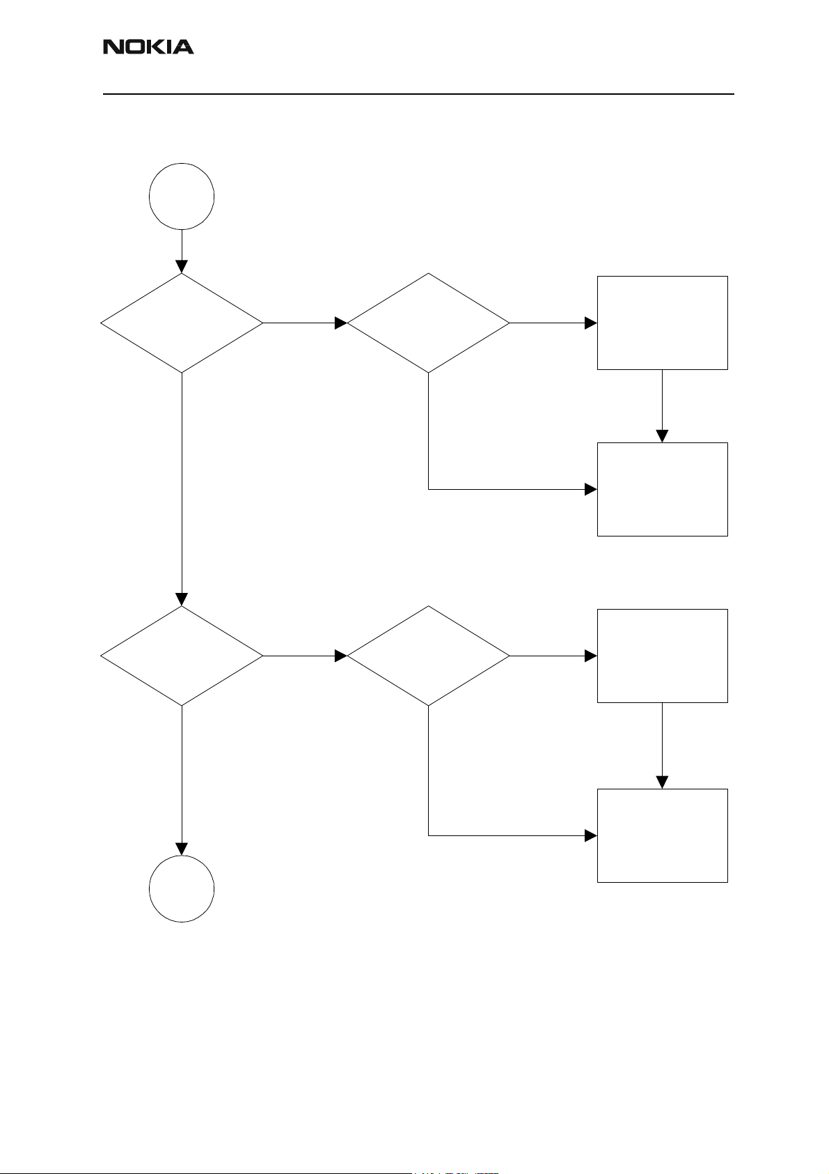
Phone is dead
This means that the phone does not use any current at all when supply is connected and/
or powerkey is pressed.
It is assumed that the voltage supplied is 3.6 VDC. The UEM will prevent any functionality what so ever at battery/supply levels below 2.9 VDC.
Original ãNokia Corporation. Page 6-5
Page 6
NPE-4
6 - Troubleshooting PAMS Technical Documentation
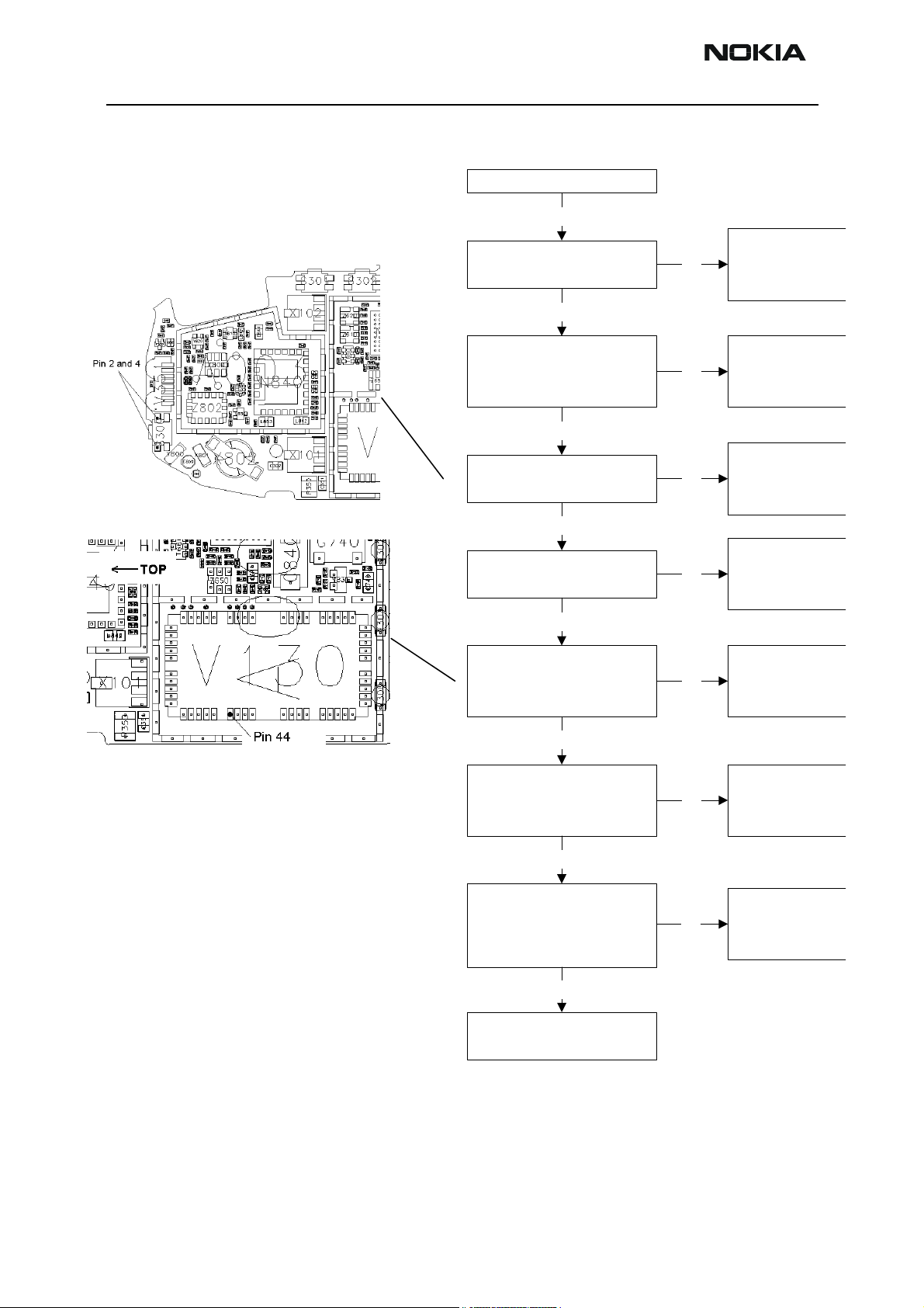
Phone is dead
Yes
L260 towards SIM connector,
VBAT = 3.6 VDC
Yes
L261 towards C261,
L262 towards C262,
L265 towards C265
voltage = 3.6 VDC
Yes
Pin 2 and 4 on S300 = 0 VDC
when powerkey pressed
Yes
Sleep clock on J404
~32.768 Hz, 1.8 Vpp
Yes
PURX = 1.8 VDC on V130
(Bluetooth module) pin44
~1 sec. after power key is
pressed
No
No
No
No
No
Failure in VBAT
line, check:
X101, X102
Check:
L261,L262,L263,
C261,C262,C265
Check:
S300, PWB
Check:
B200,C209,C210,
D200,PWB
Check:
D200, PWB
Yes
VR3 ~2.78 VDC on C295
towards D200 (UEM)
Yes
13 MHz clock min 300
mVACpp on C424 towards
D200 with regular probe Cin
~10-13 pF/10M
Yes
Check:
D400 (UPP),D450 (FLASH)
No
No
Check:
D200,C295,PWB
Check:
C424,C425,L420,
C420,R420,N600
(HAGAR)
Page 6-6 ãNokia Corporation. Original
Page 7

NPE-4
PAMS Technical Documentation 6 - Troubleshooting
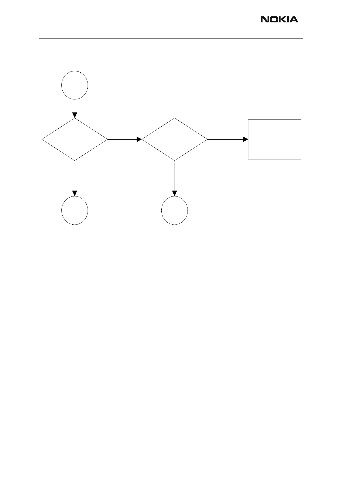
Flash programming doesn’t work
The flash programming can be done via the pads on the PWB or via system connector
X100.
In production, the first programming is done via the pads on the PWB.
The main differences between these are:
a) Flash programming voltage is produced different way.
b) Signal routings are different.
In case of Flash failure in FLALI station, problem is most likely related to SMD problems.
Possible failures could be Short circuiting of balls under µBGAs (UEM, UPP, FLASH). Missing or misaligned components.
In flash programming error cases the flash prommer can give some information about a
fault.
The fault information messages could be:
- Phone doesn't set FBUS_TX line low
The preliminary fault-finding diagrams for flash programming are shown in the next
page.
Because of the use of uBGA components it is not possible to verify if there is a short circuit in control- and address lines of MCU (UPP) and memory (flash).
Original ãNokia Corporation. Page 6-7
Page 8
NPE-4
6 - Troubleshooting PAMS Technical Documentation
Flash programming
Flash programming doesn't work
If fault information from Prommer is:
Phone doesn't set FBUS_TX line low
Yes
Check the connections:
X100 p11 - R101
X100 p12 - R104
X100 p13 - R100
Connection ok?
Yes
Try reading MCU ID
with Phenix
Reading ok?
Yes
Try reading Flash ID with
Phenix
reading ok?
Yes
Flash again
No
Solder / replace faulty
component
No
Replace either UEM or UPP
No
Replace Flash
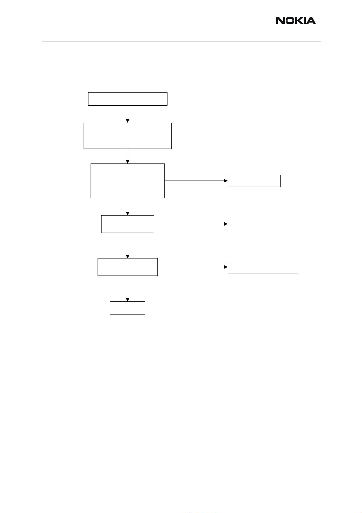
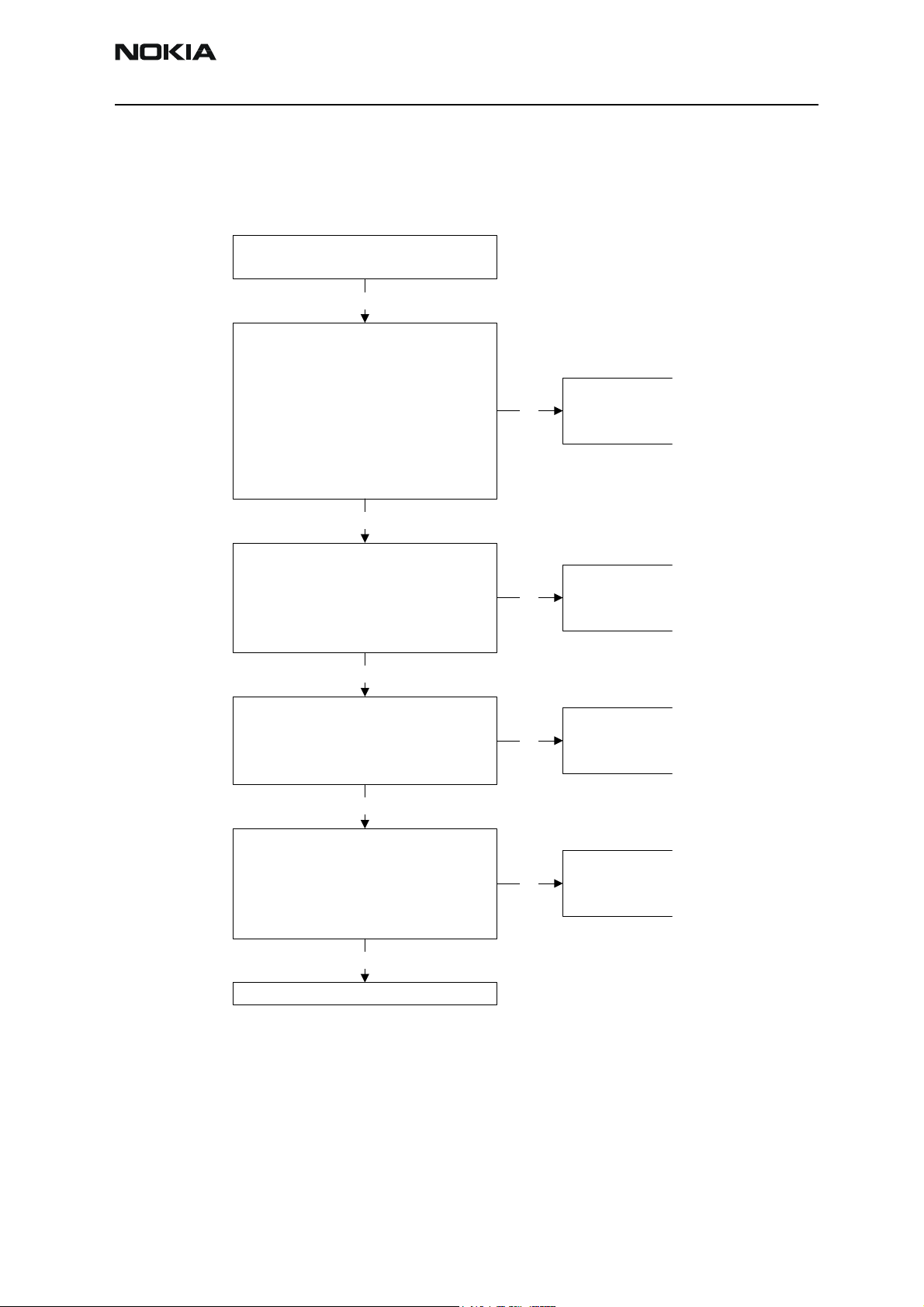
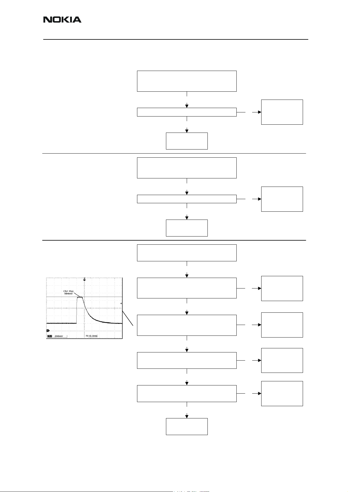
Power doesn’t stay on, or phone is jammed
If this kind of failure is presenting itself immediately after FLALI, it is most likely caused
by ASICs missing contact with PWB.
If for some reason the MCU does not service the watchdog register within the UEM, the
operations watchdog will run out after approximately 32 seconds. Unfortunately, the
service routine can not be measured.
Page 6-8 ãNokia Corporation. Original
Page 9
NPE-4
PAMS Technical Documentation 6 - Troubleshooting
Power doesn't stay on or
phone is jammed
Yes
Sleep clock on J404
~32.768 Hz, 1.8 Vpp
Yes
PURX = 1.8 VDC on V130
(Bluetooth module) pin44
~1 sec. after power key is
pressed
Yes
UI functionality and keys react
to pressure
Yes
13 MHz clock min 300
mVACpp on C424 towards
D200 with regular probe Cin
~10-13 pF/10M
Yes
TBA
No
No
No
No
Check:
B200,C209,C210,
D200,PWB
Check:
D200,PWB
Check:
D400,D450,Z300,
Keymat,
Lightguide,PWB
Check:
C424,C425,L420,
C420,R420,N600
(HAGAR)
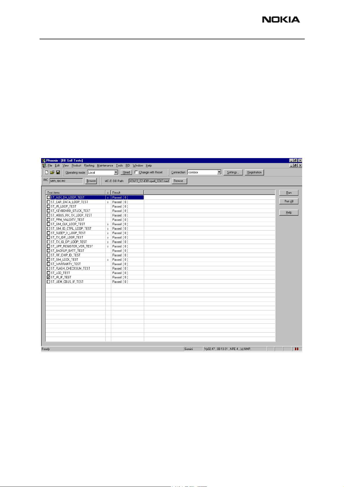
Display Information: “Contact Service”
When this error appears in the display, it means that one or more of the internally Baseband tests has failed. The Baseband tests (selftests) are performed each time the phone is
powered on. The selftests are devided into those performed while powering up (Start up
tests), and the ones that can be executed with a PC using Phoenix (Runtime tests). The
following Start-up tests are performed during power up:
UPP Register verfication test.
UEM CBUS Interface test.
SleepX loop test.
Aux. Data loop test.
Ear Data loop test.
Tx IDP loop test.
Tx IQ DP loop test.
SIM Clock loop test.
Original ãNokia Corporation. Page 6-9
Page 10
NPE-4
6 - Troubleshooting PAMS Technical Documentation
SIM I/O Control loop test.
SIM Lock test.
PMM (Flash) Validity test.
PMM (Flash) Checksum test.
If all these selftests are passed, the phone will start-up.
From Phoenix it is possible to run all the selftest and the additional "Runtime test". The
test cases can be seen below.
Page 6-10 ãNokia Corporation. Original
Page 11
NPE-4
PAMS Technical Documentation 6 - Troubleshooting
The phone doesn’t register to the network or phone doesn’t make a call
If the phone doesn't register to the network, the fault can be in either BB or RF. Due to
the highly module design of the BB area, very few signals can be measured.
Phone doesn't register to network
or phone doesn't make a call
Yes
C292 towards D200 (UEM) ~4.75 VDC
C294 towards R308 ~2.78 VDC
C295 towards UEM ~2.78 VDC
C296 towards V311 ~2.78 VDC
C297 towards UEM ~2.78 VDC
C298 towards R307 ~2.78 VDC
C299 towards V311 ~2.78 VDC
C288 towards R306 = 1.35 VDC
C289 towards UEM = 1.35 VDC
all during GSM frame. Use TXP on J760.
No
Check:
D200, D400,PWB
Yes
Check RF serial bus:
RFBUSCLK on J731/J735
RFBUSDA on J732/J76
RFBUSEN1X on J730/J734
Transitions "1" <-> "0",
1.8 VDC <-> 0 VDC during GSM frame
Yes
Check analog signals during
GSM frame (Rx slot):
RXINP on C724 towards C716 = 0-1.45 VDC
RXQINP on C725 towards C716 = 0-1.45 VDC
Yes
Check analog common mode signals during
GSM frame (Tx slot):
TXIOUTP on R764 pin 1 towards R766 and
TXIOUTN on pin 3 = 1-1.75 VDC
TXQOUTP on R766 pin 1 towards R764and
PXQOUTN on pin 3 = 1-1.75 VDC
Yes
No
No
No
Check:
D400,PWB
Check:
D200,D400,PWB
Check:
D200,D400,R764,
R766,PWB
Check RF
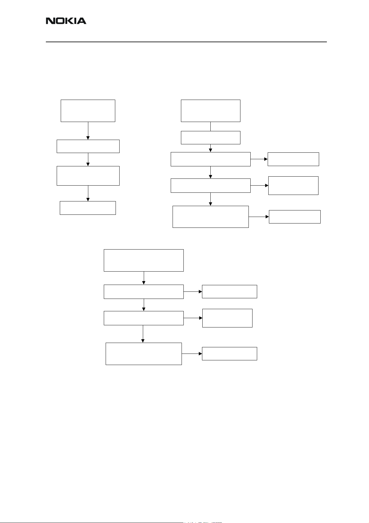
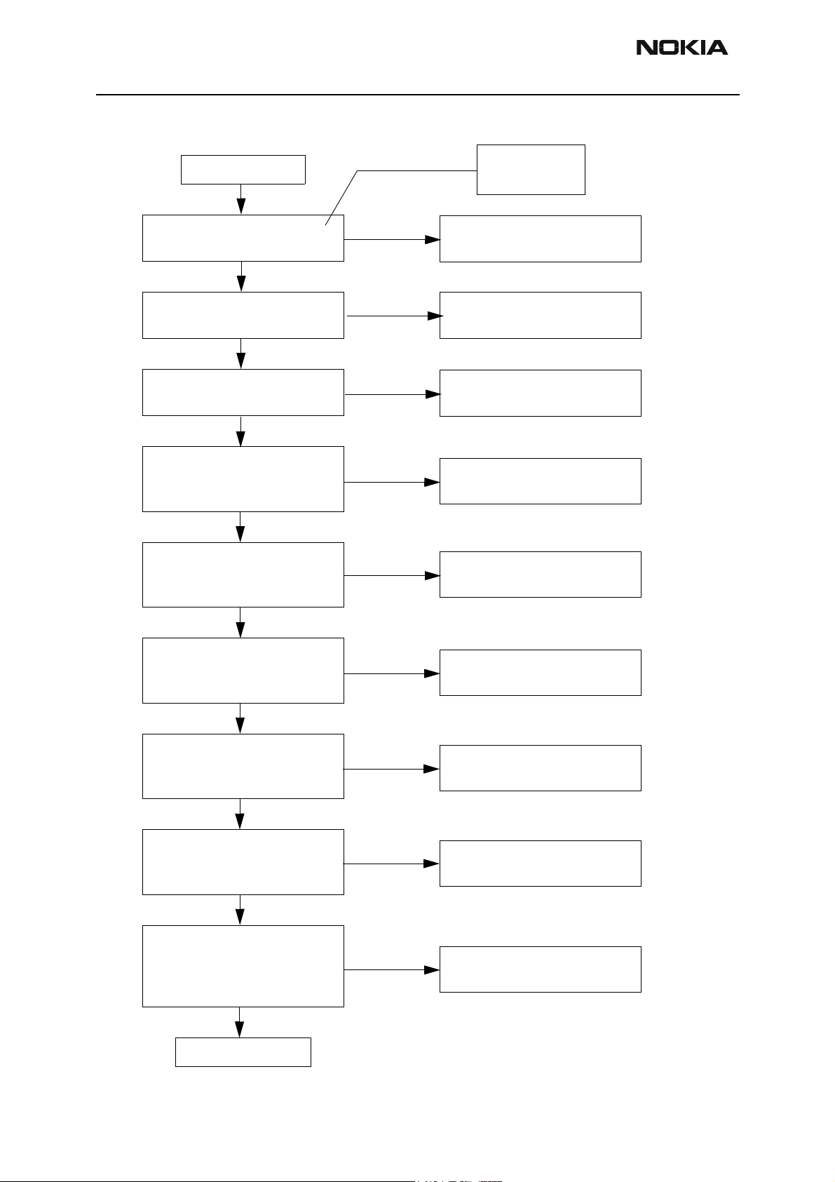
SIM Failure
The hardware of the SIM interface from UEM (D200) to the SIM connector (X386) can be
tested without a SIM card. When the power is switched on the phone first check for a
1,8V SIM card and then a 3V SIM card. The phone will try this four times, whereafter it
will display "Insert SIM card".
Original ãNokia Corporation. Page 6-11
Page 12
NPE-4
6 - Troubleshooting PAMS Technical Documentation
The error ”SIM card rejected” means that the ATR message received from SIM card is corrupted, e.g. data signal levels are wrong. The first data is always ATR and it is sent from
card to phone.
SIM Fault
Measure
VSIM at
X386. Is it
3V?
Yes
Check SIM power-up
sequence
Check SIM
No No
reader X386
Measure
VSIM at
C302. Is it
3V?
Yes
Replace R388
UEM FAILURE
VSIM
Reset
Clock
Data
Page 6-12 ãNokia Corporation. Original
Page 13
NPE-4
PAMS Technical Documentation 6 - Troubleshooting
Display Failure
Display
Fault
Is
display
working
Yes
No
Change
display
module
Is
display
working
Yes
No
Measure
Vflash1 is
2,78V
Yes
Measure
Vio is
1,8V
Turn phone off and
No
No
ohm measure
between Vflash1
and ground.
UEM FAILURE
Turn phone off and
ohm measure
between Vio and
~46k ohm
ground.
0 ohm
0R
Check C239, C279,
C304, C309, C350
R174, R202 and R352.
Check C207, C218,
C303, C404, C405,
C450, C451 and R173.
OK
Measure
Vout at
C302 is
~10,7V
UPP FAILUREEND
Yes
Yes
UEM FAILURE
No
Check C302
~510k ohm
OK
OK
Original ãNokia Corporation. Page 6-13
Page 14
NPE-4
6 - Troubleshooting PAMS Technical Documentation
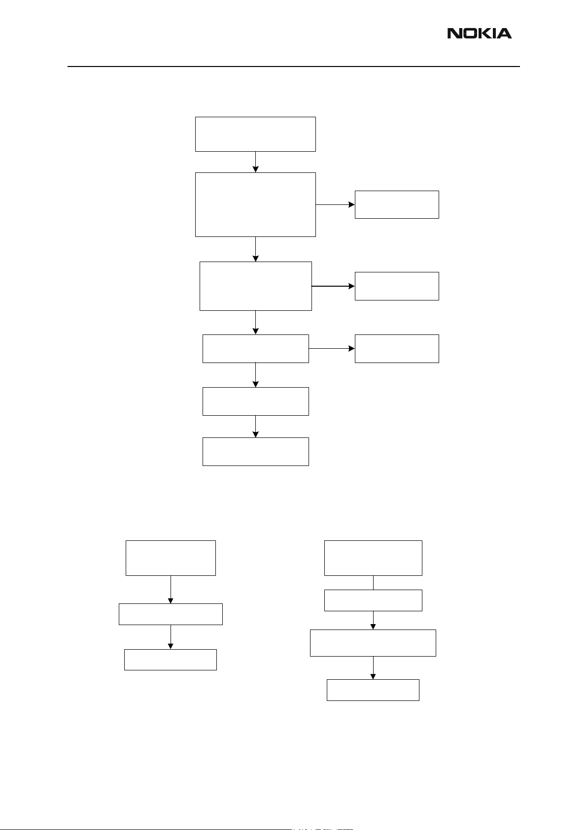
Keypad Failure
Power key failure
Keypad
fault
Power Key
OK?
Yes
No
Voltage on S300
approx = Vbat
Yes
Voltage on S300
while pressed
approx = Vbat
Yes
S300 ok ?
No
No
No
Check C312 and
Z300
If Ok ->
UEM fail
Phone
jammed
Change S300
Yes
Keypad
fault 2
Page 6-14 ãNokia Corporation. Original
Phone
dead
Page 15
NPE-4
PAMS Technical Documentation 6 - Troubleshooting
Volume key failure
Keypad
fault 2
Volume UP key
OK?
Yes
Volume DOWN key
OK?
No
No
Check S301 with
Ohmmeter
S301 short?
Yes
Check S302 with
Ohmmeter
S302 short?
No
No
Replace S301
If still fail
Replace Z300
If still fail->
UPP failure
Replace S302
If still fail
Yes
Keypad
fault 3
Yes
Replace Z300
If still fail->
UPP failure
Original ãNokia Corporation. Page 6-15
Page 16
NPE-4
6 - Troubleshooting PAMS Technical Documentation
Keyboard failure
Keypad
fault 3
Keyboard
OK?
Yes
END
No
Replace light guide
OK now?
Yes
END
No
Replace Z300
if still fail ->
UPP failure
Page 6-16 ãNokia Corporation. Original
Page 17
NPE-4
PAMS Technical Documentation 6 - Troubleshooting
Audio faults
Earpiece doesn't work
and there isn't any
mechanical problem
Replace Earpiece
Ok
Check L158, R171 (and
C150 and R156 for
Shortcircuit)
Ok
UEM FAILURE (D200)
Headset microphone doesn't work
and there isn't any
mechanical problem
Microphone doesn't work
and there isn't any
mechanical problem
Replace Microphone
Ok
R150 towards UEM (bias) = 2.1V UEM FAILURE (D200)
R151 towards miclines (bias) = 1.0-
Check MIC line to UEM:
L155, R153,C156, C155, R151,
Ok
Yes
1.4 V
Yes
C154, R152
No
Check R150, R151,
No
V158, C151, C153,
C152
Ok
UEM FAILURE (D200)
R162 towards UEM (bias) = 2.1V UEM FAILURE (D200)
R163 towards miclines (bias) = 0.8-
Check XMIC line to UEM:
L168, R167, C168, C167, C166,
C165, R166, C164, R165
Ok
Yes
1.4 V
Yes
No
Check R162, R163,
No
V151, C160, C162,
Ok
UEM FAILURE (D200)
C161
Original ãNokia Corporation. Page 6-17
Page 18
NPE-4
6 - Troubleshooting PAMS Technical Documentation
Headset earpiece doesn't work
and there isn't any
mechanical problem
With headset connected,
measure C177 and C178
towards UEM - DC level 0.8V.
Press keypad tone 5 and
measure with oscilloscope. An
AC signal pressents.
OK
Not OK
UEM FAILURE
Buzzer doesn't work
and there isn't any
mechanical problem
Measure C158 towards N150
with an oscilloscope. Same
AC signal present (higher
level).
OK
Measure R179 towards UPP
- DC level > 1.5V
OK
Check L150, R183, C158
(and C159, R161 for
Shortcircuit)
OK
Check R176, C179, R177,
R178, R180, C176, C177
and C178.
Not OK
Not OK
Vibra doesn't work
and there isn't any
mechanical problem
BOOMER FAILURE
UPP FAILURE
Check vibra
Replace Buzzer
Ok
UEM FAILURE (D200)
Check L307, C307, C308
UEM FAILURE (D200)
Ok
Ok
Page 6-18 ãNokia Corporation. Original
Page 19
NPE-4
PAMS Technical Documentation 6 - Troubleshooting
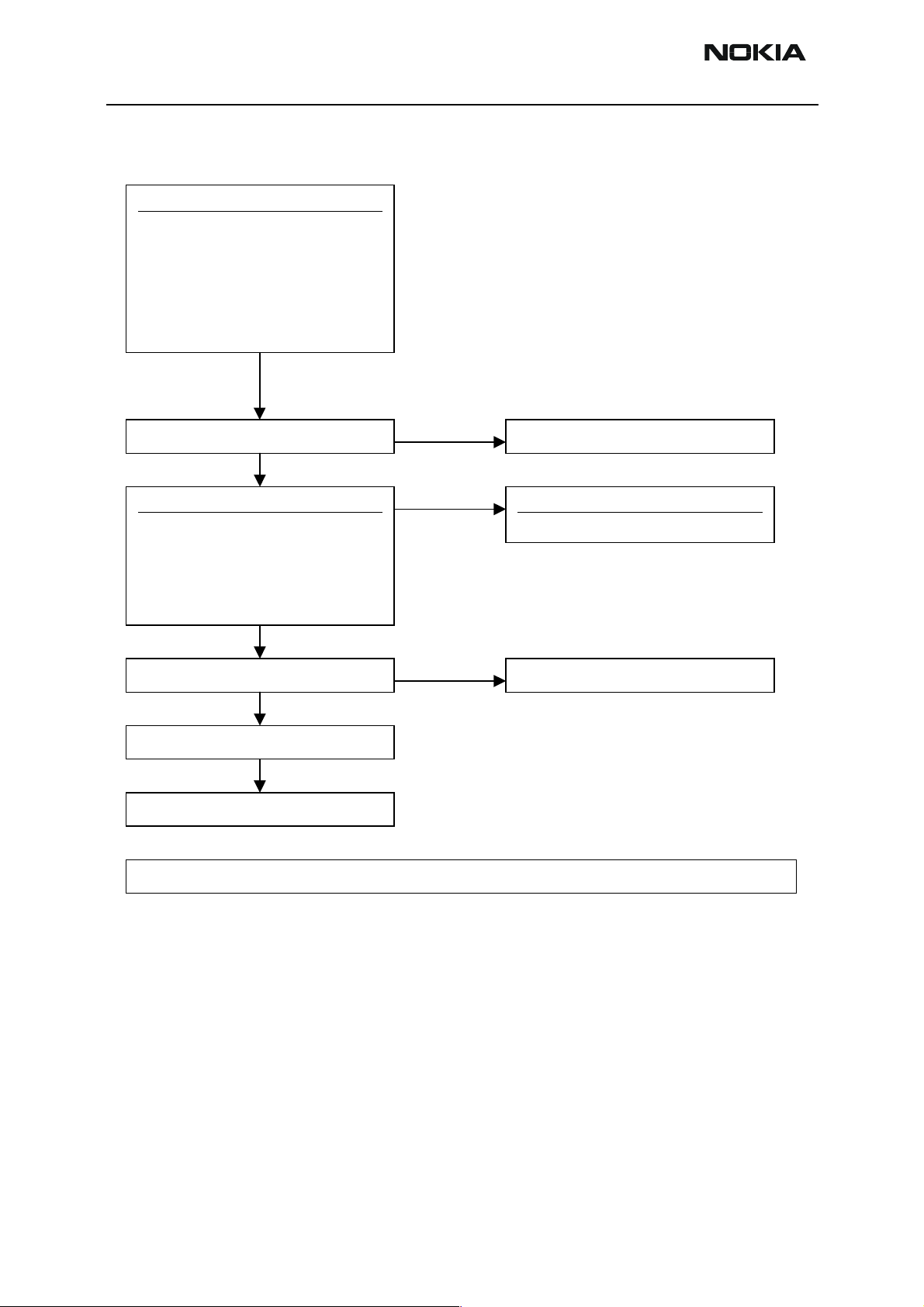
Charger failure
Phone is off - battery is completely empty
(~3.1 VDC) and no current is drawn from
charger when connected
Yes
Check:
VCHAR > 2.1 VDC on L100 towards C107
Yes
D200 UEM is
faulty
Phone is on or off - battery has norminal
voltage 3.6 VDC and no current is drawn from
charger when connected
Yes
VCHAR > 2.1 VDC on L100 towards C107
Yes
No
No
F100, L100, V101,
C107
Check:
F100, L100, V101,
C107
Check:
D200, D400
Display information when charger connected:
"Not charging"
Yes
Voltage on R240 towards D200 (UEM)
~0.8 VDC when power is connected. BSI
value must be 39K (BPS-2, BLS-2)
Yes
Voltage (Use Scope) on R220 towards D200
(UEM) ~0.9 VDC at peak. BTEMP value must
be 47K.
Yes
Voltage on R200 towards D200 (UEM) same
as VBAT voltage
Yes
Voltage slowly rises on R200 towards D200
(UEM) when charger is connected
No
No
No
No
Check:
X101,
R202,R240,C240
Check:
X102,R202,R220,
C220
Check:
R200, D200
Check:
D200, PWB
Yes
Check:
PWB
Original ãNokia Corporation. Page 6-19
Page 20
NPE-4
6 - Troubleshooting PAMS Technical Documentation
Blue Tooth module faults
Flashing fails
V130 P52, P53, P54
VBAT = 3,6V
Yes
V130 P6, L133 P2
VREG = 2,7 - 2,86V
Yes
V130 P32, P49, P18
VAPPL = 1,7 - 3,3V
Yes
V130 P50
SYSCLK 0,5 - 0,8Vampl
26MHz (10ppm)
Yes
V130 P26
SLEEPCLK = 1,8V
32,768kHz (5%)
No
No
No
No
No
None easy
accessable
Failure in VBAT line
check X101 and X102
Faulty PWB or UEM
Faulty PWB or UEM
Faulty PWB or N600
Faulty PWB or UEM
Yes
V130 P34
CBUS_Enx = 0V
When bus is active
Yes
V130 P36
CBUS_CLK = 1,8V
1MHz
Yes
V130 P35
CBUS_Da = 1,8v
Data
Yes
V130 P37
LPRFint = 1,8v
Pulses of approx. 20ms
When BT is on in UI
Yes
No
No
No
No
Faulty PWB or UEM
Faulty PWB or UEM
Faulty PWB or UEM
Faulty PWB or UEM
Replace module
Page 6-20 ãNokia Corporation. Original
Page 21
NPE-4
N
N
N
t
NoN
N
N
N
PAMS Technical Documentation 6 - Troubleshooting
o BT air connection
Antenna open circui
Yes
Faulty PWB
o BT audio connection
J143
USARTTx = 1,8V
Data
Yes
J144
USARTRx = 1,8V
Data
Yes
o
o
o
V130 bad soldering
V130 bad soldering
V130 bad soldering
o
o
Replace module
V130
Replace module
V130
Replace module
V130
Faulty PWB
Original ãNokia Corporation. Page 6-21
Page 22
NPE-4
N
N
K
N
N
6 - Troubleshooting PAMS Technical Documentation
RF Fail
The problem is most likely RF related
if the following conditions are
fulfilled.
Module can be flashed and BER
·
Test can be initiated.
BER is above limit or no
·
connection to BT-Box
Visual soldering inspection Re-solder
O
Measure SYSCLK > 200 mVpp
Reference: 11pF probe.
ote: The measured result can depend
very much on the probe type.
Tip: If nessesary, measure a known
good prototype with the same probe.
YES
Measure Vreg » 2.8 volts
YES
Replace MCM
Re-flash BT only
ot OK
O
O
VCTCXO or Buffer failure
See RF troubleshooting document
Check VFLASH1 & L133
Test points can be seen in the document “Baseband testpoints”.
Page 6-22 ãNokia Corporation. Original
Page 23

NPE-4
PAMS Technical Documentation 6 - Troubleshooting
RF Troubleshooting
Introduction
Measurements should be done using Spectrum Analyzer with high-frequency highimpedance passive probe (LO-/reference frequencies and RF-power levels) and Oscilloscope with a 10:1 probe (DC-voltages and low frequency signals).
The RF-section is build around one ASICS Hagar (N600). For easier troubleshooting, this
RF troubleshooting document is divided into sections.
Before changing Hagar, please check the following things: Supply voltages are OK and
serial communication are coming to Hagar (See Baseband troubleshooting document).
Please note that the grounding of the PA-module is directly below PA-module so it is
difficult to check or change. Most RF semiconductors are static discharge sensitive!
So ESD protection must be taken during repair (ground straps and ESD soldering irons).
The Hagar IC is moisture sensitive so parts must be pre-baked prior to soldering.
Apart from key-components described in this document here are a lot of discrete components (resistors, inductors and capacitors) which troubleshooting is done by checking if
soldering of the component is done properly, for factory repairs (checking if it is missing
from PCB). Capacitors can be checked for shortening and resistors for value by means of
an ohmmeter, but be aware in-circuit measurements should be evaluated carefully.
Please be aware that all measured voltages or RF levels in this document are rough
figures. Especially RF levels varies due to different measuring equipment or different
grounding of the used probe.
All tuning must be done with Phoenix Service Software, version 02.90.001, or later.
Original ãNokia Corporation. Page 6-23
Page 24
NPE-4
6 - Troubleshooting PAMS Technical Documentation
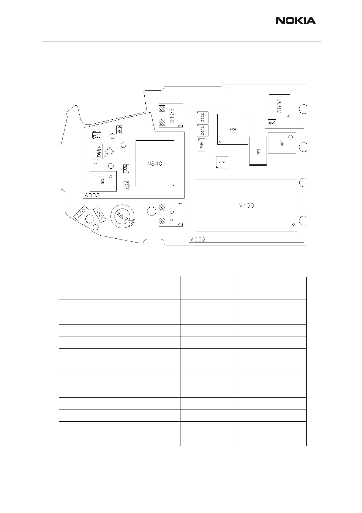
RF Key component placement
Reference
number
N600 HAGAR RF IC X802 RF Connector
N840 PA L836 Directional Coupler
Z610 PCN RX SAW filter V830 Detector Diode
Z620 EGSM RX SAW filter X101 Battery Terminal V+
Z650 EGSM TX SAW filter X102 Battery Terminal V-
Z804 RX DUAL SAW filter G630 VCO
Z802 RXTX Switch Module G740 VCTCXO
T660 PCN TX Balun T630 VCO Balun
V810 PCN RX LNA C840 Supply Capacitor
V820 EGSM RX LNA V130 Bluetooth Module
X800 Antenna signal clip A002 HAGAR RF Can
X801 Antenna ground clip A003 PA Can
Name
Reference
number
Name
Page 6-24 ãNokia Corporation. Original
Page 25

PAMS Technical Documentation 6 - Troubleshooting
RF Measurement points
PA Can
Measurement points are shown on the picture below inside the circles.
RF
Connector
VBD
PA EGSM out
PA
PCN out
DUAL SAW
PCN in
DUAL SAW
EGSM PCN in
VANT1 VANT2 LNAB_900
NPE-4
V820 RF out
LNAC_900
V820 RF in
DUAL SAW
EGSM out
DUAL SAW
PCN out
VTXB_900
TX_900
V810 RF in
V810 RF out
LNAB_ 1800
TX_1800 VTXB_1800
Original ãNokia Corporation. Page 6-25
Page 26
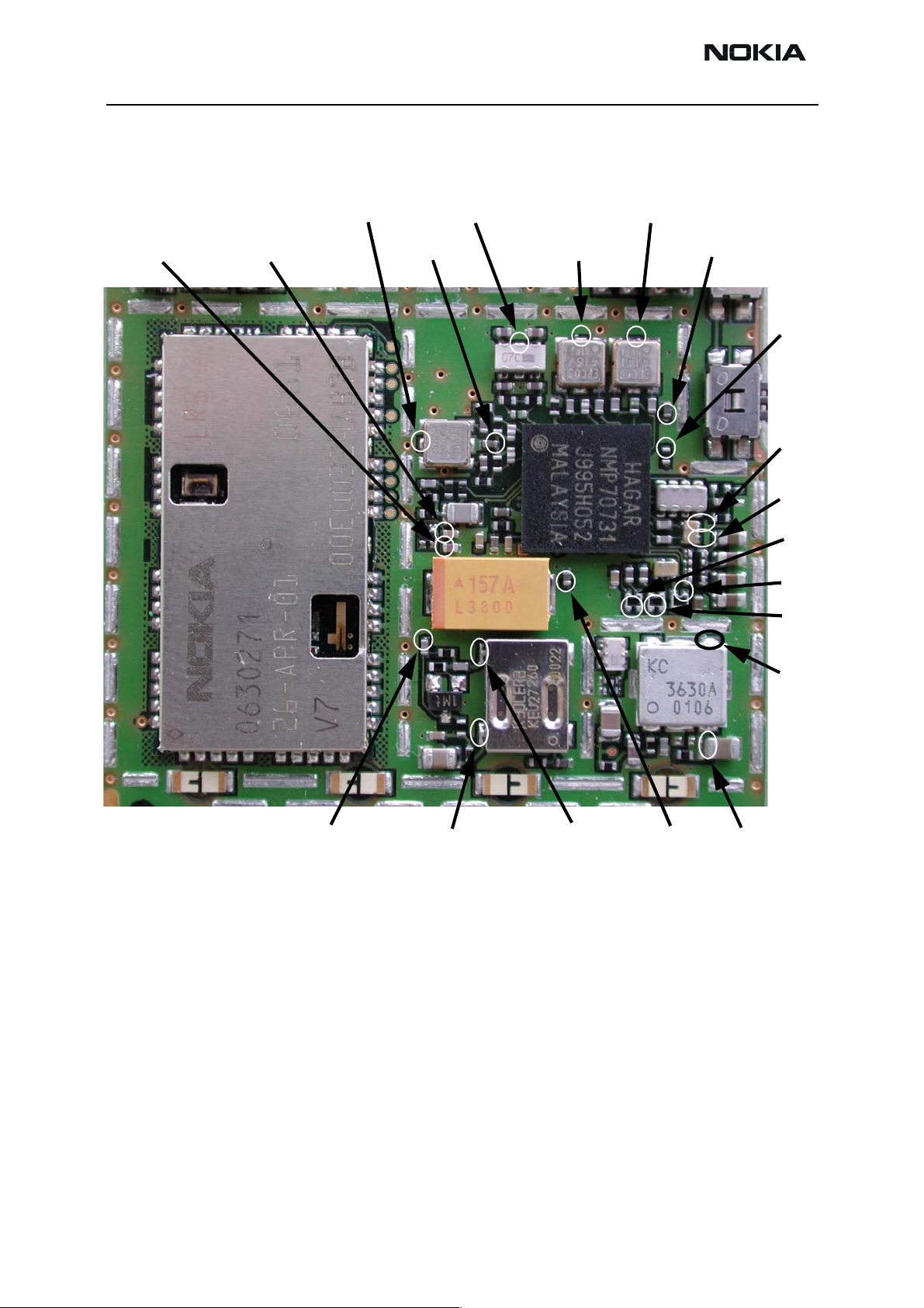
NPE-4
6 - Troubleshooting PAMS Technical Documentation
Hagar RF can
Measurement points are shown circled on the picture below.
TXP
TXC
TX_900
TX_1800
VR2
Z610 input
Z620 input
VR4
LNAC_1800
RXIINP
RXQINP
TXQOUT
P/N
VREFRF01
TXIOU
P/N
Bluetooth
Clockbuffer
output
VCO out
VCTCXO supply VCTCXO out VR3 VCO supply
Page 6-26 ãNokia Corporation. Original
Page 27

NPE-4
PAMS Technical Documentation 6 - Troubleshooting
Abbreviations in fault finding charts
BB Baseband
DC Direct Current
EGSM Extended GSM (See section 9.6.1 for frequency range)
ESD Electro Static Dicharge
f: Frequency of signal (measured with Spectrum Analyzer)
GPRS General Packed Radio Service
HSCSD High Speed Circuit Switched Data
LO Local Oscillator
P: Power of signal in decibels (dB) (measured with Spectrum Analyzer)
PA Power Amplifier
PCB Printed Circuit Board
PCN GSM1800 (See section 9.6.2 for frequency range)
PLL Phase Locked Loop
RF Radio Frequency
RX Receiver
T: Time between pulses
TX Transmitter
UHF Ultra High Frequency
V: Voltage of signal (measured with oscilloscope)
VCO Voltage controlled oscillator
VHF Very High Frequency
Original ãNokia Corporation. Page 6-27
Page 28
NPE-4
6 - Troubleshooting PAMS Technical Documentation
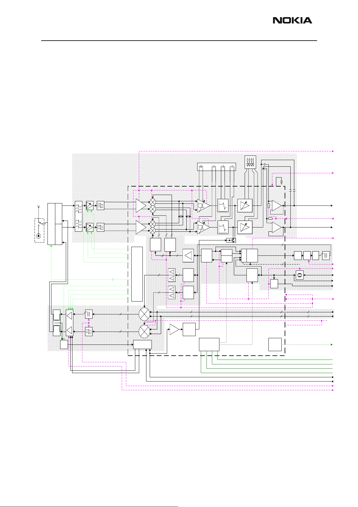
RF in general
The RF part of this product is a Dualband Direct Conversion transceiver (Also used in
6210, 8210, 8850, 8310, and other). In Direct Conversion no intermediate frequencies are
used for up- or downconversion. The VCO is set to either twice or four times (depending
on the band used) the wanted RX or TX Frequency. The VCO frequency is divided by either
2 or 4 and fed to the mixers (down-conversion) or modulators (up-conversion). Up- or
down-conversion is done in one step, directly between RF frequency and DC. All up and
down-conversion takes place in the RF IC named Hagar (N600). Hagar also contains PLL
and a DC control section used to power and/or control LNAs, TX buffers, Detector and RX/
TX Switch. Hagar is controlled via a serial bus (CTRL).
VRF_RX
Hagar
Cp_f_I
Cm_f_I
Cp_f_Q
Cp_dtos_I
Cm_dtos_I
Cp_dtos_Q
Cm_dtos_Q
Cm_f_Q
OUT_BB1_I
OUT_BB1_Q
I_DCN2_I
C1_BB1_I
C2_BB1_I
I_DCN2_Q
C2_BB1_Q
C1_BB1_Q
VB_EXT
RB_EXT
VR4
VREFRF01
DUAL
SAW
RX
PCN
TX
RX
Ant Switch
GSM
Antenna connector
C:\USERS\HCS\HDb13\Troubleshooting\pics\Blocks\HDb13_block_010806.vsd
TX
Dir. Coupler
DET
PA
VBATTRF
LOIS RF Block Diagram
Last edit 10:39 06-08-01
LNA
BALUN
SAW
INP_P_RX
INM_P_RX
SAW
LNA
SAW
INP_G_RX
INM_G_RX
LNAB_G
LNAB_P
LNA_G
LNA_P
V_ANT_1/
V_ANT_2
2
VBD
VTXLO_G
VTX_B_G
VTX_B_P
OUTP_P_TX/
OUTM_P_TX
OUTP_G_TX/
OUTM_G_TX
DET
j
BB_Gain
0-40dB
BB_Gain
0-40dB
charge
pump
RDIV
DNC2
DNC2
1/2
RF TEMP
SENSOR
2
2
2
RXI
VREF_RX
RXQ
INP_LO/INM_LO
OUT_CP
loop
VCO
2dB
filter
VCP/GND_CP
VDIG
OSC_IN
TOUT
VBB
VF_RX
VPRE
VLO
TXI_0/TXI_180
TXQ_0/TXQ_180
GNDRF_TX
GND_BB / GNDRF_RX / GND_LO / GND_PRE /
GND_CP / GND_ DIG / GND_RX
RFTEMP
AFC
26MHz
TXIOUTP/TXIOUTN
2
TXQOUTP/TXQOUTN
2
VREFRF02
RXQ
AFC
LPRFCLK _I
RFCLK_I
HGR_TEMP
RFBUSEN1
RFBUSCLK
RFBUSDA
RESET
VBATTRF
RXI
VCP
VR7
VR3
VR4
TXC
TXP
VR2
BIQUAD
DtoS
8 / 18 dB
BIQUAD
DtoS
222
2
1/4
1/2
2
2
2
RF
Controls
Open collector
2
Open collector
2
PWC
Vpctrl_g
Vpctrl_p
44
TXP
TXC
44
0dB
Calibration
8 / 18 dB
64/65
NDIV
ADIV
1/2
1/4
2
2 2
RX Filter
CTRL
SLE
SCLK
SDATA
Reset
The RF supports HSCSD (High Speed Circuit Switched Data) and GPRS (General Packed
Radio Service), meaning multislot operation, this will not require special equipment or
procedures in repair situations.
Page 6-28 ãNokia Corporation. Original
Page 29

NPE-4
PAMS Technical Documentation 6 - Troubleshooting
EGSM Receiver
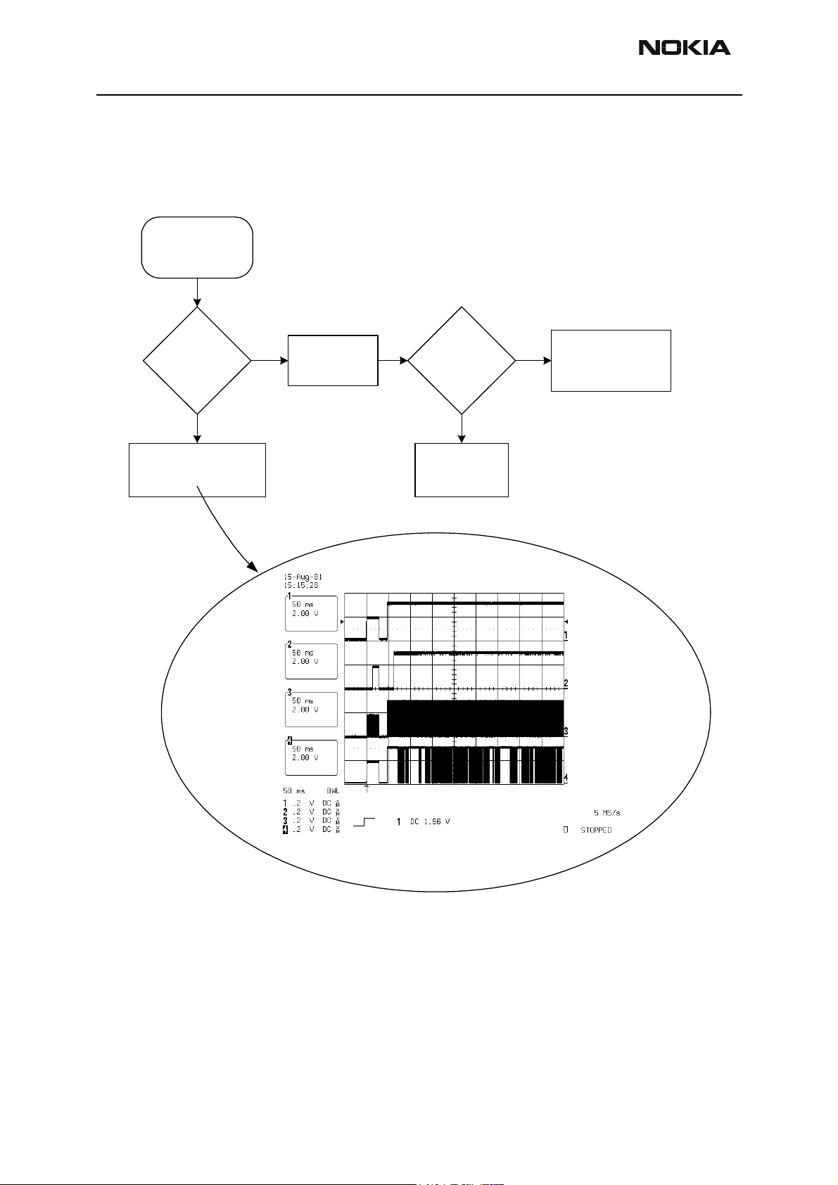
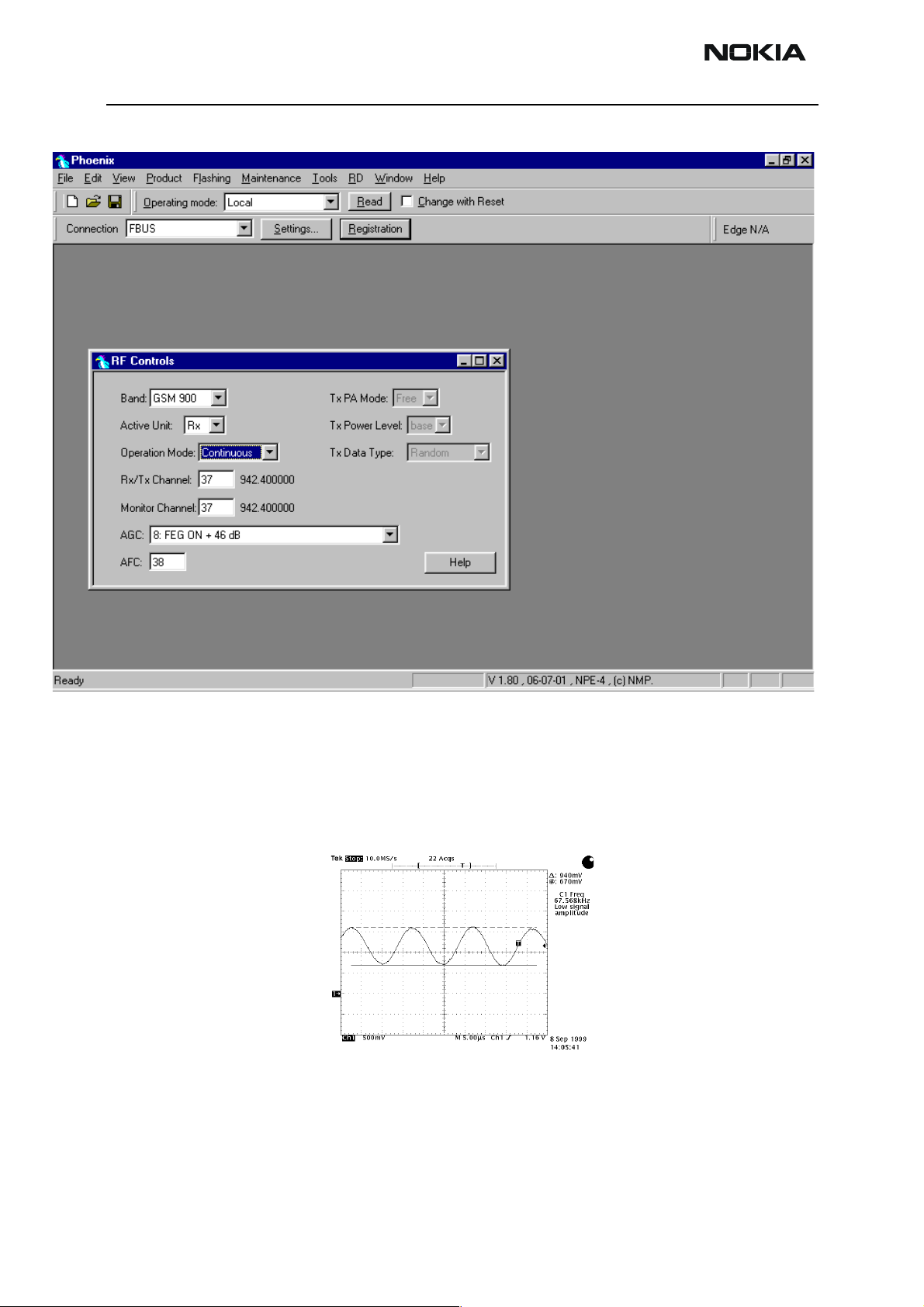
General instructions for EGSM RX troubleshooting
Connect the the phone to a PC with DAU-9P cable and dongle and follow the following
instructions:
Start Phoenix Service Software
Select File Alt-F
Scan Product Ctrl-R
Wait until phone information shows in the lower right corner of the screen.
Set operating mode to local mode
Select Maintenance Alt-M
Tuning T
RF Controls F
Wait until the RF Controls window pops up
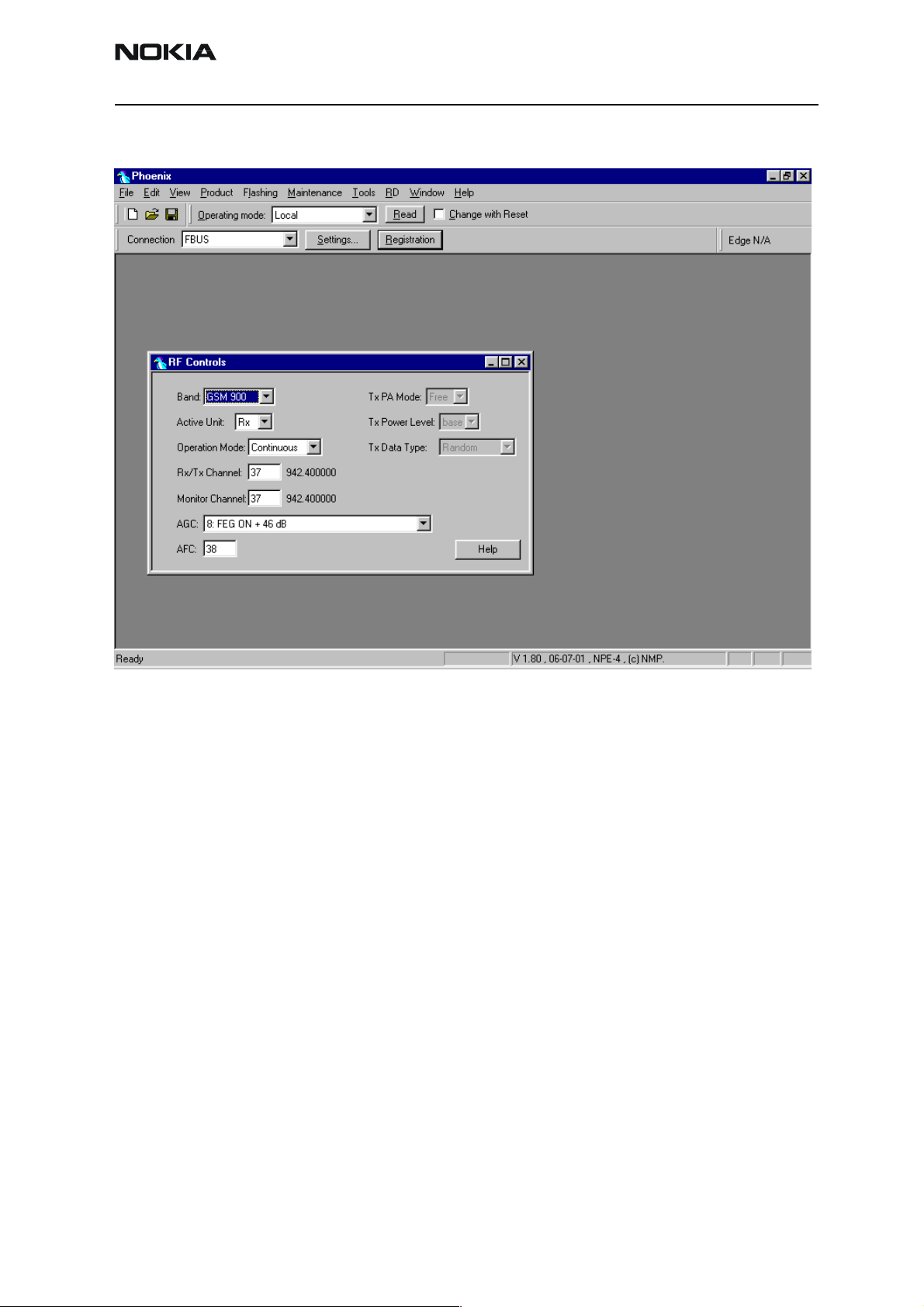
Select Band GSM 900
Active unit RX
Operation mode Continuous
RX/TX Channel 37
AGC 8
The setup should now look like this:
Original ãNokia Corporation. Page 6-29
Page 30
NPE-4
6 - Troubleshooting PAMS Technical Documentation
Apply a 942.467 MHz (channel 37 + 67.710kHz offset) -80 dBm signal to the RF-connector (remember to compensate for cable attenuation).
Measuring with an oscilloscope on “RXIINP” or “RXQINP” this picture should be seen on a
working EGSM receiver:
Signal amplitude 950mV
DC offset 1,1V
Frequency 67kHz
If this picture is not seen, then go to troubleshooting.
Page 6-30 ãNokia Corporation. Original
Page 31

NPE-4
PAMS Technical Documentation 6 - Troubleshooting
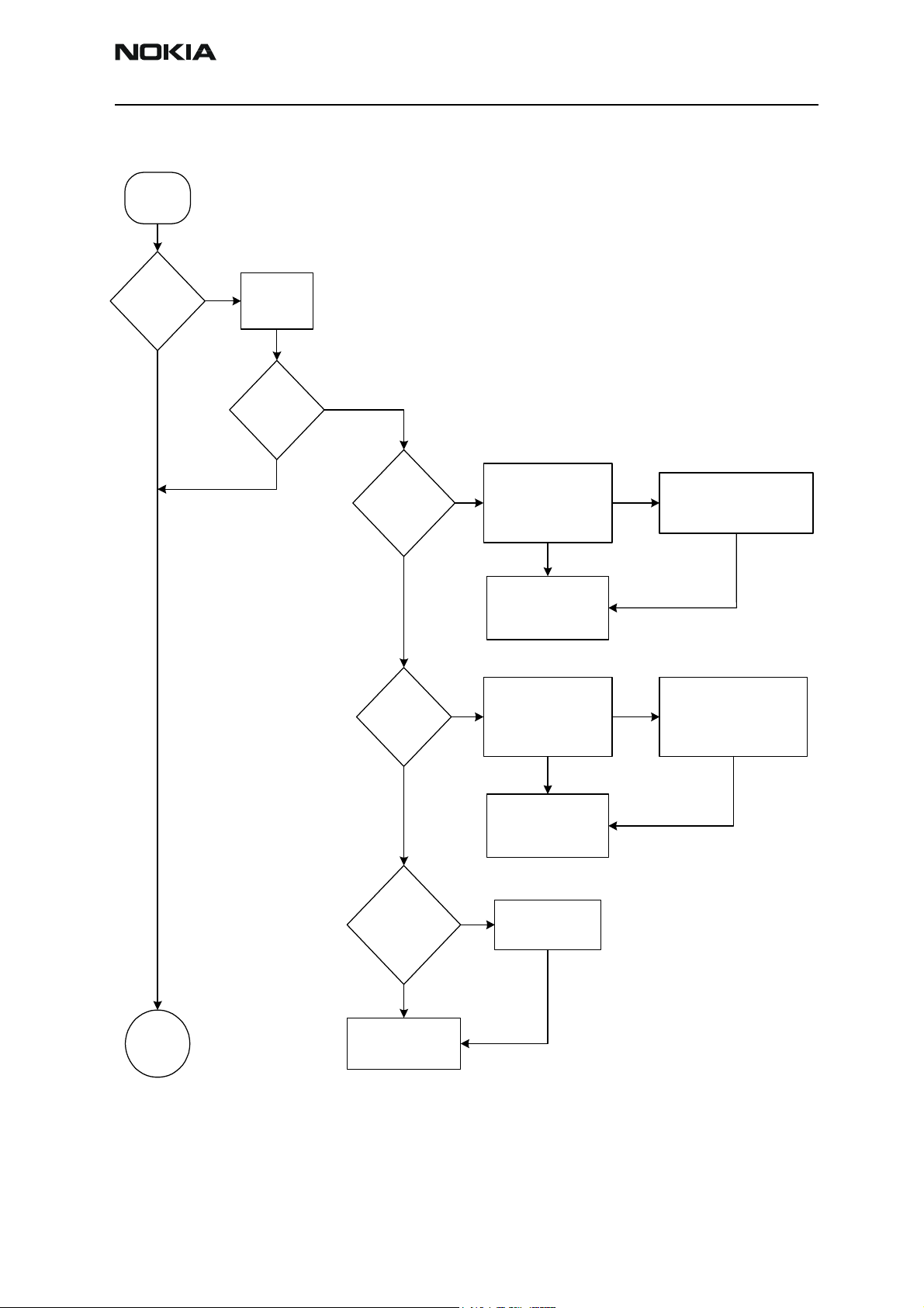
Fault finding chart for EGSM receiver
Apply -80dBm
942.467MHz signal from
generator to antenna
connector
Yes
Oscilloscope at RXIINP
Signal 950mVpp
DC offset 1,1V
Frequency 67,7kHz
Yes
EGSM chain functional
Change generator
No No
level to -55dBm
EGSM Signal path
EGSM RX Fault finding Tree
Spectrumanalyzer
Yes
Spectrumanalyzer
Check Hagar serial
V820, RFout
-73dBm
Yes
Z620 input
-75dBm
Yes
Oscilloscope
VR4 2.7V
interface
Yes
Check Hagar
N600
Spectrumanalyzer
DUAL SAW
(Z804) EGSM out
-85dBm
Oscilloscope
LNAC_900
2.4-2.8V
LNAB_900 0V
Yes
Oscilloscope
V820, RFout 2.1-2.2V
V820, RFin 0.8-0.9V
Yes
Check
No
Yes
V820
Check
C824
Spectrumanalyzer
No
No
Check
R822,R823,R828,
No
V820,C821,C822,
C828, L822
Check BBNo
Oscilloscope
VR4 2.7V
Check Hagar serial interface
Yes
Check Hagar
N600
Check BaseBandNo
DUAL SAW
(Z804) EGSM in
-84dBm
Yes
Check Z804
No
Check RX/TX
Switch
Z802
For easy error tracing it is important to know the signal path of the EGSM receiver. The
compnents can be grouped into blocks and drawn as shown below. Note that the picture
shows bothe EGSM receiver (bottom) and PCN (top).
RX/TX Switch
From the antenna-pad (X800) the RF signal is lead to the RX/TX switch (Z802) via a
mechanical switch, the antenna connector (X802).
Tba
Original ãNokia Corporation. Page 6-31
Page 32

NPE-4
6 - Troubleshooting PAMS Technical Documentation
If no control voltage is present at VC1 or VC2 the RX/TX switch is open to the two RX
outlets GSM_Rx and DCS_Rx. The RX/TX switch will work as a diplexer and EGSM signals
pass to GSM_Rx and PCN signals to DCS_Rx.
From GSM_Rx the EGSM signal is feed to the Dual RX SAW filter (Z804) via C804.
Front-end
The EGSM front-end consists mainly of two SAW filters (Z804 and Z620) and one LNA
(V820) in-between. The SAW filters provides out-of-band blocking immunity, the LNA
provides front-end gain. The first SAW filter (Z804) is a DUAL package including SAW filter for both EGSM and PCN. The last SAW filter (Z620) is single ended input and balanced output providing a balanced signal input for Hagar (N600).
The signal-path is through Z804 (In-band insertion-loss 3,5dB), through the matching
circuit (L821, L820 and C821) and to the EGSM LNA (V820, RFin).
nd
From the LNA (V820, RF out) the signal is lead through C824, through the 2
SAW Z620 (In-band insertion-loss 3,5dB), through the balanced matching circuit (C626,
C627, L626) to Hagar (N600).
EGSM
Hagar
The balanced RX signal is mixed with a signal from the local oscillator at the same frequency as the wanted RX signal. After mixing the signal is converted to a single ended
signal in the DtoS (Differential to Single ended) amplifier. The signal is now filtered in a
BIQUAD filter to provide channel separation, amplified in the BB_Gain amplifier and DC
compensated in DCN2.
PCN Receiver
General instructions for PCN RX troubleshooting
Connect the the phone to a PC with DAU-9P cable and dongle and follow the following
instructions:
Start Phoenix Service Software
Select File Alt-F
Scan Product Ctrl-R
Wait until phone information shows in the lower right corner of the screen.
Set operating mode to local mode
Select Maintenance Alt-M
Tuning T
RF Controls F
Page 6-32 ãNokia Corporation. Original
Page 33

NPE-4
PAMS Technical Documentation 6 - Troubleshooting
Wait until the RF Controls window pops up
Select Band GSM 1800
Active unit RX
Operation mode Continuous
RX/TX Channel 700
AGC 8
The setup should now look like this:
Apply a 1842.867 MHz (channel 700 + 67.710kHz offset) -80 dBm signal to the RF-connector (remember to compensate for cable attenuation).
Original ãNokia Corporation. Page 6-33
Page 34

NPE-4
6 - Troubleshooting PAMS Technical Documentation
Measuring with an oscilloscope on “Hagar RXI” or “Hagar RXQ” this picture should be
seen on a working PCN receiver:
Signal amplitude 1.5V
DC offset 1,1V
Frequency 67kHz
If this picture is not seen, then go to section 6.2 of this document for troubleshooting.
Fault finding chart for PCN receiver
Apply -80dBm
1842.867MHz signal
from generator to
antenna connector
Yes
Oscilloscope at RXIINP
Signal 1.5Vpp
DC offset 1.1V
Frequency 67.7kHz
Yes
PCN chain functional
Change generator
No No
level to -55dBm
PCN RX Fault finding Tree
Spectrumanalyzer
Yes
Spectrumanalyzer
Check Hagar serial
V810, RFout
-72dBm
Yes
Z610 input
-75dBm
Yes
Oscilloscope
VR4 2.7V
interface
Yes
Spectrumanalyzer
(Z804) PCN out
LNAB_1800 0V
Oscilloscope
V810, RFout 2.1-2.2V
V810, RFin 0.8-0.9V
No
DUAL SAW
-92dBm
Yes
Oscilloscope
LNAC_1800
2.4-2.8V
Yes
Yes
Check
V810
Check
C814
Spectrumanalyzer
No
No
Check
R812,R813,R818,
No
V810,C811,C812,
C818, L812
Check BBNo
Oscilloscope
VR4 2.7V
Check Hagar serial int erface
Yes
Check Hagar
N600
Check BaseBandNo
DUAL SAW
(Z804) PCN in
-91dBm
Yes
Check Z804
No
Check RX/TX
Switch
Z802
Check Hagar
N600
Page 6-34 ãNokia Corporation. Original
Page 35

NPE-4
PAMS Technical Documentation 6 - Troubleshooting
PCN Signal path
For easy error tracing it is important to know the signal path of the PCN receiver. The
components can be grouped into blocks and drawn as shown below. Note that the picture shows both EGSM recieiver (bottom) and PCN receiver (top).
Tba
RX/TX Switch
From the antenna-pad (X800) the RF signal is lead to the RX/TX switch (Z802) via a
mechanical switch, the antenna connector (X802).
If no control voltage is present at VC1 or VC2 the RX/TX switch is open to the two RX
outlets GSM_Rx and DCS_Rx. The RX/TX switch will work as a diplexer and EGSM signals
pass to GSM_Rx and PCN signals to DCS_Rx.
From DCS_Rx the PCN signal is feed to the Dual RX SAW filter (Z804) via C806.
Front-end
The PCN front-end consists mainly of two SAW filters (Z804 and Z610) and one LNA
(V810) in-between. The SAW filters provides out-of-band blocking immunity, the LNA
provides front-end gain. The first SAW filter (Z804) is a DUAL package including SAW filter for both EGSM and PCN. The last SAW filter (Z610) is single ended input and balanced
output providing a balanced signal input for Hagar (N600).
The signal-path is through Z804 (In-band insertion-loss max 4dB), through C811 to the
PCN LNA (V810, RFin).
From the LNA (V810, RF out) the signal is lead through C814, through the 2nd EGSM SAW
Z610 (In-band insertion-loss max 4dB), through the balanced matching circuit (C616,
C617, L616) to Hagar (N600).
Original ãNokia Corporation. Page 6-35
Page 36

NPE-4
6 - Troubleshooting PAMS Technical Documentation
Hagar
The balanced RX signal is mixed with a signal from the local oscillator at the same frequency as the wanted RX signal. After mixing the signal is converted to a single ended
signal in the DtoS (Differential to Single ended) amplifier. The signal is now filtered in a
BIQUAD filter to provide channel separation, amplified in the BB_Gain amplifier and DC
compensated in DCN2.
EGSM Transmitter
General instructions for EGSM TX troubleshooting
Apply a RF-cable to the RF-connector to allow the transmitted signal to act as normal.
RF-cable should be connected to measurement equipment (GSM Test equipment, Powermeter, Spectrum Analyzer, or similar) or to at least a 10-dB attenuator, otherwise the PA
may be damaged.
Connect the the phone to a PC with DAU-9P cable and dongle and follow the following
instructions:
Start Phoenix Service Software
Select File Alt-F
Scan Product Ctrl-R
Wait until phone information shows in the lower right corner of the screen.
Set operating mode to local mode
Select Maintenance Alt-M
Tuning T
RF Controls F
Wait until the RF Controls window pops up
Select Band GSM 900
Active unit TX
Operation mode Burst
RX/TX Channel 37
TX PA Mode Free
TX Power Level 10
TX Data Type Random
Page 6-36 ãNokia Corporation. Original
Page 37

NPE-4
PAMS Technical Documentation 6 - Troubleshooting
The setup should now look like this:
Now the measurement equipment should measure the following output signal from the
phone.
· P
+23dBm @ 897.4MHz
out
If this is not the case, then go to the fault finding chart for EGSM transmitter in this document for troubleshooting.
Original ãNokia Corporation. Page 6-37
Page 38

NPE-4
6 - Troubleshooting PAMS Technical Documentation
Path of the transmitted EGSM signal
For easy error tracing it is important to know the signal path of the EGSM transmitter.
The components can be grouped into blocks and drawn as shown below. Note that the
picture shows both EGSM transmitter (bottom) and PCN transmitter (top).
HAGAR
V_ANT_1/
V_ANT_2
2
VBD
VTXLO_G
VTX_B_G
VTX_B_P
RF
Controls
Antenna connector
Hagar
PA
Dir. Coupler
RX
PCN
TX
RX
Ant Switch
GSM
TX
PA
DET
VBATTRF
BALUN
SAW
OUTP_P_TX/
OUTM_P_TX
2
OUTP_G_TX/
OUTM_G_TX
2
DET
Open collector
Open collector
Vpctrl_g
TXI_0/TXI_180
2
TXQ_0/TXQ_180
2
PWC
Vpctrl_p
TXP
TXC
TXIOUTP/TXIOUTN
2
TXQOUTP/TXQOUTN
2
VBATTRF
The Balanced TX signal from baseband is coming to the RF IC Hagar. It includes RF modulators, one for EGSM and one for PCN. The Baseband signal is mixed with the LO signal
corresponding to the wanted TX channel. The PCN TX output of Hagar is a balanced signal.
From the output of Hagar the signal goes through the EGSM TX SAW filter (Balanced to
single ended) to the PA EGSM input.
TXC
TXP
VR2
The PA EGSM part has a maximum output at app. 35dBm. The supply is coming directly
from the Battery terminals.
The output is controlled by Hagar by the power control loop. From the ouput of the PA
the signal goes through the directional coupler (one of the power control loop components) to the RXTX Switch.
RXTX Switch
The RXTX Switch is making the filtering between RX and TX Bands and between EGSM
and PCN bands. It is controlled by Hagar by the two voltages VANT1 and VANT2. The following table shows the different states.
VANT1 [Volt] VANT2 [Volt] EGSM Rx PCN Rx EGSM Tx PCN Tx
0 0 X X
0 2.7 X
2.7 0 X
Page 6-38 ãNokia Corporation. Original
Page 39

NPE-4
PAMS Technical Documentation 6 - Troubleshooting
Fault finding chart for EGSM transmitter
Oscilloscope
R726 VREFRF01 Vdc = 1.5 Volt Check
C656 VR2 Vdc = 2.7 Volt
C760 TXP Vdc > 2.5 Volt
C601 VR4 Vdc = 2.7 Volt
Ye s
Oscilloscope
R764 TXIOUTP 67kHz
R764 TXIOUTN 67kHz
R766 TXQOUTP 67kHz
R766 TXQOUTN 67kHz
Ye s
Oscilloscope
C856
C866 VTXB_1800 Vdc < 0.3 Volt
C808 VANT1 Vdc < 0.3 Volt
C809 VANT2 Vdc > 2.0 Volt
C830 VBD Vdc > 2.0 Volt
Ye s
Spectrum analyser No Check
Z650 out, R858 in TX_900 Power > -3 dBm, 897,4 MHz
Ye s Synthesiser
Use Wintesla to select
TX_Data Type: Random
TX Power Level: 10
Ye s
Spectrum analyser Check PA N840
L836 EGSM in
(PA N840 EGSM out)
Power = +25 dBm, 897,4 MHz Check TXC
Ye s
Spectrum analyser Check
RF-connector No Directional Coupler (L836)
Pout = +23 dBm, 897,4 MHz RX/TX Switch (Z802)
Ye s
EGSM TX
OK
VTXB_900 Vdc > 2.0 Volt No Check:
No
Vac = 0.4 Vpp, Vdc = 0.8 V
Vac = 0.4 Vpp, Vdc = 0.8 V
Vac = 0.4 Vpp, Vdc = 0.8 V
Vac = 0.4 Vpp, Vdc = 0.8 V
Check Power Loop
L836,V830
No BaseBand
No
Check
BaseBand
Hagar Serial Interface
Hagar
EGSM TX SAW Filter
Hagar
Original ãNokia Corporation. Page 6-39
Page 40

NPE-4
6 - Troubleshooting PAMS Technical Documentation
PCN Transmitter
General instructions for PCN TX troubleshooting
Apply a RF-cable to the RF-connector to allow the transmitted signal to act as normal.
RF-cable should be connected to measurement equipment (GSM Test equipment, Powermeter, Spectrum Analyzer, or similar) or to at least a 10-dB attenuator, otherwise the PA
may be damaged.
Connect the the phone to a PC with DAU-9P cable and dongle and follow the following
instructions:
Start Phoenix Service Software
Select File Alt-F
Scan Product Ctrl-R
Wait until phone information shows in the lower right corner of the screen.
Set operating mode to local mode
Select Maintenance Alt-M
Tuning T
RF Controls F
Wait until the RF Controls window pops up
Select Band GSM 1800
Active unit TX
Operation mode Burst
RX/TX Channel 700
TX PA Mode Free
TX Power Level 5
TX Data Type Random
Page 6-40 ãNokia Corporation. Original
Page 41

NPE-4
PAMS Technical Documentation 6 - Troubleshooting
The setup should now look like this:
Now the measurement equipment should measure the following output signal from the
phone.
· P
+20dBm @ 1747.8MHz
out
If this is not the case, then go to the fault finding chart for PCN transmitter in this document for troubleshooting.
Path of the transmitted PCN signal
For easy error tracing it is important to know the signal path of the PCN transmitter. The
components can be grouped into blocks and drawn as shown below. Note that the picture shows both EGSM transmitter (bottom) and PCN transmitter (top)
Original ãNokia Corporation. Page 6-41
Page 42

NPE-4
6 - Troubleshooting PAMS Technical Documentation
HAGAR
V_ANT_1/
V_ANT_2
2
VBD
VTXLO_G
VTX_B_G
VTX_B_P
RF
Controls
Antenna connector
Hagar
Dir. Coupler
RX
PCN
TX
RX
Ant Switch
GSM
TX
PA
DET
VBATTRF
BALUN
SAW
OUTP_P_TX/
OUTM_P_TX
2
OUTP_G_TX/
OUTM_G_TX
2
DET
Open collector
Open collector
Vpctrl_g
TXI_0/TXI_180
2
TXQ_0/TXQ_180
2
PWC
Vpctrl_p
TXP
TXC
TXIOUTP/TXIOUTN
2
TXQOUTP/TXQOUTN
2
VBATTRF
The Balanced TX signal from baseband is coming to the RF IC Hagar. It includes RF modulators, one for EGSM and one for PCN. The Baseband signal is mixed with the LO signal
corresponding to the wanted TX channel. The output of Hagar is a balanced signal.
From the PCN TX output of Hagar the signal goes through the PCN TX Balun (Balanced to
single ended) to the PA PCN TX input.
TXC
TXP
VR2
PA
The PA PCN part has a maximum output at app. 32dBm. The supply is coming directly
from the Battery terminals.
The output is controlled by Hagar by the power control loop. From the ouput of the PA
the signal goes through the directional coupler (one of the power control loop components) to the RXTX Switch.
RXTX Switch
The RXTX Switch is making the filtering between RX and TX Bands and between EGSM
and PCN bands. It is controlled by Hagar by the two voltages VANT1 and VANT2. The following table shows the different states.
VANT1 [Volt] VANT2 [Volt] EGSM Rx PCN Rx EGSM Tx PCN Tx
0 0 X X
0 2.7 X
2.7 0 X
Page 6-42 ãNokia Corporation. Original
Page 43

NPE-4
PAMS Technical Documentation 6 - Troubleshooting
Fault finding chart for PCN transmitter
Oscilloscope
R726 VREFRF01 Vdc = 1.5 Volt Check
C656 VR2 Vdc = 2.7 Volt No BaseBand
C760 TXP Vdc > 2.5 Volt
C601 VR4 Vdc = 2.7 Volt
C602 VR3 Vdc = 2.7 Volt
Yes
Oscilloscope
R764 TXIOUTP 67kHz
R764 TXIOUTN 67kHz
R766 TXQOUTP 67kHz
R766 TXQOUTN 67kHz
Yes
Oscilloscope
C856 VTXB_900 Vdc < 0.3 Volt No Check:
C866 VTXB_1800 Vdc > 2.0 Volt Hagar Serial Interface
C808 VANT 1 Vdc > 2.0 Volt Hagar
C809 VANT 2 Vdc < 0.3 Volt
C830 VBD Vdc > 2.0 Volt
Yes
Spectrum analyser No Check
T660 out, L868 TX_1800 Power > -3 dBm, 1747,8 MHz PCN TX Balun
Yes Synthesiser
Use Wintesla to select
TX_Data Type: Random
TX Power Level: 5
Yes
Spectrum analyser Check PA N840
L836 PCN in
(PA N840 PCN out)
Power = +22 dBm, 1747,8 MHz Check TXC
Yes
Spectrum analyser Check
RF-connector No Directional Coupler (L836)
Pout = +20 dBm, 1747,8 MHz RX/TX Switch (Z802)
Yes
PCN TX
OK
No Check Power Loop
Vac = 0.4 Vpp, Vdc = 0.8 V
Vac = 0.4 Vpp, Vdc = 0.8 V
Vac = 0.4 Vpp, Vdc = 0.8 V
Vac = 0.4 Vpp, Vdc = 0.8 V
L836,V830
No Check
BaseBand
Hagar
Synthesiser
There is only one PLL synthesiser generating frequencies for both Rx and Tx in both bands
Original ãNokia Corporation. Page 6-43
Page 44

NPE-4
6 - Troubleshooting PAMS Technical Documentation
(EGSM and PCN). VCO frequency is divided by 2 or by 4 in HAGAR depending on which
band is active.
General instructions for Synthesiser troubleshooting
Connect the the phone to a PC with DAU-9P cable and dongle and follow the following
instructions:
Start Phoenix Service Software
Select File Alt-F
Scan Product Ctrl-R
Wait until phone information shows in the lower right corner of the screen.
Set operating mode to local mode
Select Maintenance Alt-M
Tuning T
RF Controls F
Wait until the RF Controls window pops up
Select Band GSM 900
Active unit RX
Operation mode Continuous
RX/TX Channel 37
Page 6-44 ãNokia Corporation. Original
Page 45
NPE-4
PAMS Technical Documentation 6 - Troubleshooting
The setup should now look like this:
Now it is possible to measure frequency of 3769.6MHz at the output of the VCO (G630)
using a resistive probe and a spectrum analyzer.
If this is not the case, then go to fault finding chart for PLL synthesiser in this document
for troubleshooting.
26 MHz reference oscillator ( VCTCXO )
The 26 MHz oscillator (G740) has three functions.
= Reference frequency for the PLL synthesiser.
= System clock for BB (13 MHz) after it is divided by 2 in HAGAR.
= 26 MHz Reference clock for Bluetooth Module (V130).
26 MHz signal from the VCTCXO is approx. 0,8 Vpp. Frequency of this oscillator is
adjusted by dc voltage (Vcon) coming from the DAC in UEM (D200). Range of Vcon is 0.3
– 2.3 V.
Original ãNokia Corporation. Page 6-45
Page 46
NPE-4
6 - Troubleshooting PAMS Technical Documentation
VCO
The VCO is able to generate frequencies in the range of 3420 – 3840 MHz when PLL is in
function. The frequency of the VCO signal is divided by 2 or by 4 in HAGAR so it is possible to generate the frequency of all channels in EGSM and PCN (both RX and TX). Frequency of the VCO is controlled by DC voltage (Vc) coming from the loop filter. Range of
the Vc when PLL is in function is 0.7 – 3.8 V. Even if PLL is not working (Vc out of range)
there is some frequency at the output of the VCO which is between 3 and 4 GHz (if the
VCO itself is ok).
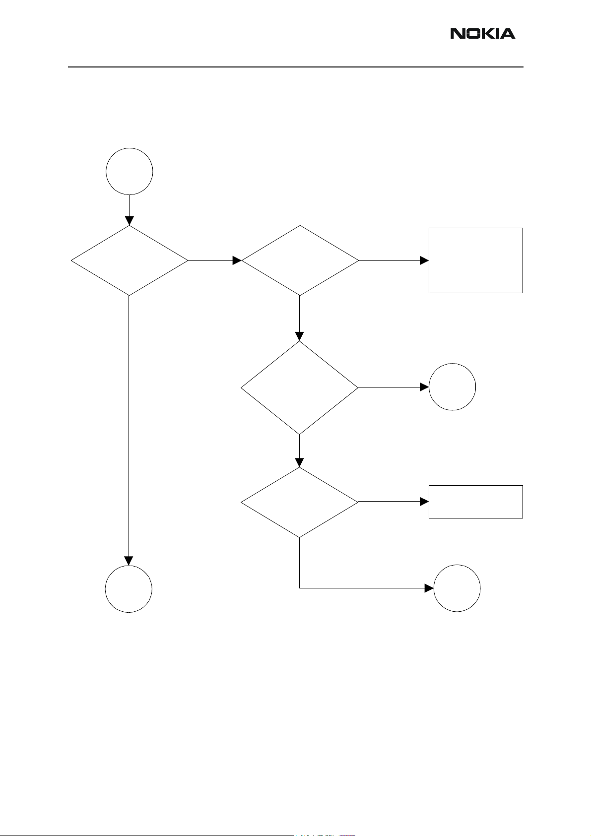
Fault finding chart for PLL Synthesiser
Setup with Phoenix:
Band: GSM 900
Mode: RX Continuous
Channel: 37
Yes
Spectrumanalyzer
VCO out (G630 out)
3769.6 MHz
Yes
Oscilloscope
Bluetooth Clockbuffer
output (LPRFCLK_I)
(C753)
26MHz
Yes
PLL Block is functional
Oscilloscope
No
No
VCTCXO Supply
(G740 Vcc)
Check UEM,
Software??
Phone not in function
Check Bluetooth
Clockbuffer
R750,R751,R752,
V831,C752,C753
2.7V
No
PLL Synthesiser Fault finding Tree
Oscilloscope
Yes
VCTCXO output
(G740 out)
26MHz,app.0.8Vpp
VCTCXO is dead
Check HAGAR,
Wrong writing to HAGAR
Yes
No
Yes
Oscilloscope
VCO Supply
(G630 Vcc)
Check UEM,
Software??
Phone not in function
Spectrumanalyzer
VCO out (G630 out)
Some signal 3-4 GHz
VCTCXO is dead
2.7V
No
Yes
No
It is important to say that power supply for VCTCXO ( VXO) is OFF only in ‘Deep Sleep
Mode’ and power supply for VCO (G630 Vcc) is OFF in ‘Sleep Mode’.
Page 6-46 ãNokia Corporation. Original
Page 47

NPE-4
PAMS Technical Documentation 6 - Troubleshooting
PLL Blockdiagram
2
2 2 2
1/4
1/2
2
2
44
2
1/2
64/65
NDIV
ADIV
INP_LO/INM_LO
2
charge
j
pump
RDIV
1/2
OUT_CP
VCP/GND_CP
2
VDIG
OSC_IN
TOUT
loop
filter
VCO
AFC
26MHz
2dB
VCP
VR7
VR3
AFC
LPRFCLK_I
RFCLK_I
1/4
44
VBB
VF_RX
VPRE
VLO
VR4
CTRL
SLE
SCLK
SDATA
Reset
RFBUSEN1
RFBUSCLK
RFBUSDA
RESET
Original ãNokia Corporation. Page 6-47
Page 48

NPE-4
6 - Troubleshooting PAMS Technical Documentation
Frequency lists
EGSM
CH TX RX VCO TX VCO RX CH TX RX VCO TX VCO RX CH TX RX VCO TX VCO RX
975 880.2 925.2 3520.8 3700.8 1 890.2 935.2 3560.8 3740.8 63 902.6 947.6 3610.4 3790.4
976 880.4 925.4 3521.6 3701.6 2 890.4 935.4 3561.6 3741.6 64 902.8 947.8 3611.2 3791.2
977 880.6 925.6 3522.4 3702.4 3 890.6 935.6 3562.4 3742.4 65 903 948 3612 3792
978 880.8 925.8 3523.2 3703.2 4 890.8 935.8 3563.2 3743.2 66 903.2 948.2 3612.8 3792.8
979 881 926 3524 3704 5 891 936 3564 3744 67 903.4 948.4 3613.6 3793.6
980 881.2 926.2 3524.8 3704.8 6 891.2 936.2 3564.8 3744.8 68 903.6 948.6 3614.4 3794.4
981 881.4 926.4 3525.6 3705.6 7 891.4 936.4 3565.6 3745.6 69 903.8 948.8 3615.2 3795.2
982 881.6 926.6 3526.4 3706.4 8 891.6 936.6 3566.4 3746.4 70 904 949 3616 3796
983 881.8 926.8 3527.2 3707.2 9 891.8 936.8 3567.2 3747.2 71 904.2 949.2 3616.8 3796.8
984 882 927 3528 3708 10 892 937 3568 3748 72 904.4 949.4 3617.6 3797.6
985 882.2 927.2 3528.8 3708.8 11 892.2 937.2 3568.8 3748.8 73 904.6 949.6 3618.4 3798.4
986 882.4 927.4 3529.6 3709.6 12 892.4 937.4 3569.6 3749.6 74 904.8 949.8 3619.2 3799.2
987 882.6 927.6 3530.4 3710.4 13 892.6 937.6 3570.4 3750.4 75 905 950 3620 3800
988 882.8 927.8 3531.2 3711.2 14 892.8 937.8 3571.2 3751.2 76 905.2 950.2 3620.8 3800.8
989 883 928 3532 3712 15 893 938 3572 3752 77 905.4 950.4 3621.6 3801.6
990 883.2 928.2 3532.8 3712.8 16 893.2 938.2 3572.8 3752.8 78 905.6 950.6 3622.4 3802.4
991 883.4 928.4 3533.6 3713.6 17 893.4 938.4 3573.6 3753.6 79 905.8 950.8 3623.2 3803.2
992 883.6 928.6 3534.4 3714.4 18 893.6 938.6 3574.4 3754.4 80 906 951 3624 3804
993 883.8 928.8 3535.2 3715.2 19 893.8 938.8 3575.2 3755.2 81 906.2 951.2 3624.8 3804.8
994 884 929 3536 3716 20 894 939 3576 3756 82 906.4 951.4 3625.6 3805.6
995 884.2 929.2 3536.8 3716.8 21 894.2 939.2 3576.8 3756.8 83 906.6 951.6 3626.4 3806.4
996 884.4 929.4 3537.6 3717.6 22 894.4 939.4 3577.6 3757.6 84 906.8 951.8 3627.2 3807.2
997 884.6 929.6 3538.4 3718.4 23 894.6 939.6 3578.4 3758.4 85 907 952 3628 3808
998 884.8 929.8 3539.2 3719.2 24 894.8 939.8 3579.2 3759.2 86 907.2 952.2 3628.8 3808.8
999 885 930 3540 3720 25 895 940 3580 3760 87 907.4 952.4 3629.6 3809.6
1000 885.2 930.2 3540.8 3720.8 26 895.2 940.2 3580.8 3760.8 88 907.6 952.6 3630.4 3810.4
1001 885.4 930.4 3541.6 3721.6 27 895.4 940.4 3581.6 3761.6 89 907.8 952.8 3631.2 3811.2
1002 885.6 930.6 3542.4 3722.4 28 895.6 940.6 3582.4 3762.4 90 908 953 3632 3812
1003 885.8 930.8 3543.2 3723.2 29 895.8 940.8 3583.2 3763.2 91 908.2 953.2 3632.8 3812.8
1004 886 931 3544 3724 30 896 941 3584 3764 92 908.4 953.4 3633.6 3813.6
1005 886.2 931.2 3544.8 3724.8 31 896.2 941.2 3584.8 3764.8 93 908.6 953.6 3634.4 3814.4
1006 886.4 931.4 3545.6 3725.6 32 896.4 941.4 3585.6 3765.6 94 908.8 953.8 3635.2 3815.2
1007 886.6 931.6 3546.4 3726.4 33 896.6 941.6 3586.4 3766.4 95 909 954 3636 3816
1008 886.8 931.8 3547.2 3727.2 34 896.8 941.8 3587.2 3767.2 96 909.2 954.2 3636.8 3816.8
1009 887 932 3548 3728 35 897 942 3588 3768 97 909.4 954.4 3637.6 3817.6
1010 887.2 932.2 3548.8 3728.8 36 897.2 942.2 3588.8 3768.8 98 909.6 954.6 3638.4 3818.4
1011 887.4 932.4 3549.6 3729.6 37 897.4 942.4 3589.6 3769.6 99 909.8 954.8 3639.2 3819.2
1012 887.6 932.6 3550.4 3730.4 38 897.6 942.6 3590.4 3770.4 100 910 955 3640 3820
1013 887.8 932.8 3551.2 3731.2 39 897.8 942.8 3591.2 3771.2 101 910.2 955.2 3640.8 3820.8
1014 888 933 3552 3732 40 898 943 3592 3772 102 910.4 955.4 3641.6 3821.6
1015 888.2 933.2 3552.8 3732.8 41 898.2 943.2 3592.8 3772.8 103 910.6 955.6 3642.4 3822.4
1016 888.4 933.4 3553.6 3733.6 42 898.4 943.4 3593.6 3773.6 104 910.8 955.8 3643.2 3823.2
1017 888.6 933.6 3554.4 3734.4 43 898.6 943.6 3594.4 3774.4 105 911 956 3644 3824
1018 888.8 933.8 3555.2 3735.2 44 898.8 943.8 3595.2 3775.2 106 911.2 956.2 3644.8 3824.8
1019 889 934 3556 3736 45 899 944 3596 3776 107 911.4 956.4 3645.6 3825.6
1020 889.2 934.2 3556.8 3736.8 46 899.2 944.2 3596.8 3776.8 108 911.6 956.6 3646.4 3826.4
1021 889.4 934.4 3557.6 3737.6 47 899.4 944.4 3597.6 3777.6 109 911.8 956.8 3647.2 3827.2
1022 889.6 934.6 3558.4 3738.4 48 899.6 944.6 3598.4 3778.4 110 912 957 3648 3828
1023 889.8 934.8 3559.2 3739.2 49 899.8 944.8 3599.2 3779.2 111 912.2 957.2 3648.8 3828.8
0 890 935 3560 3740 50 900 945 3600 3780 112 912.4 957.4 3649.6 3829.6
Frequency list NPE-3 EGSM
51 900.2 945.2 3600.8 3780.8 113 912.6 957.6 3650.4 3830.4
52 900.4 945.4 3601.6 3781.6 114 912.8 957.8 3651.2 3831.2
53 900.6 945.6 3602.4 3782.4 115 913 958 3652 3832
54 900.8 945.8 3603.2 3783.2 116 913.2 958.2 3652.8 3832.8
55 901 946 3604 3784 117 913.4 958.4 3653.6 3833.6
56 901.2 946.2 3604.8 3784.8 118 913.6 958.6 3654.4 3834.4
57 901.4 946.4 3605.6 3785.6 119 913.8 958.8 3655.2 3835.2
58 901.6 946.6 3606.4 3786.4 120 914 959 3656 3836
59 901.8 946.8 3607.2 3787.2 121 914.2 959.2 3656.8 3836.8
60 902 947 3608 3788 122 914.4 959.4 3657.6 3837.6
61 902.2 947.2 3608.8 3788.8 123 914.6 959.6 3658.4 3838.4
62 902.4 947.4 3609.6 3789.6 124 914.8 959.8 3659.2 3839.2
Page 6-48 ãNokia Corporation. Original
Page 49

NPE-4
PAMS Technical Documentation 6 - Troubleshooting
PCN
CH TX RX VCO TX VCO RX CH TX RX VCO TX VCO RX CH TX RX VCO TX VCO RX CH TX RX VCO TX VCO RX
512
1710.2 1805.2 3420.4 3610.4
513
1710.4 1805.4 6841.6 7221.6
514
1710.6 1805.6 6842.4 7222.4
515
1710.8 1805.8 6843.2 7223.2
516
1711 1806 6844 7224
517
1711.2 1806.2 6844.8 7224.8
518
1711.4 1806.4 6845.6 7225.6
519
1711.6 1806.6 6846.4 7226.4
520
1711.8 1806.8 6847.2 7227.2
521
1712 1807 6848 7228
522
1712.2 1807.2 6848.8 7228.8
523
1712.4 1807.4 6849.6 7229.6
524
1712.6 1807.6 6850.4 7230.4
525
1712.8 1807.8 6851.2 7231.2
526
1713 1808 6852 7232
527
1713.2 1808.2 6852.8 7232.8
528
1713.4 1808.4 6853.6 7233.6
529
1713.6 1808.6 6854.4 7234.4
530
1713.8 1808.8 6855.2 7235.2
531
1714 1809 6856 7236
532
1714.2 1809.2 6856.8 7236.8
533
1714.4 1809.4 6857.6 7237.6
534
1714.6 1809.6 6858.4 7238.4
535
1714.8 1809.8 6859.2 7239.2
536
1715 1810 6860 7240
537
1715.2 1810.2 6860.8 7240.8
538
1715.4 1810.4 6861.6 7241.6
539
1715.6 1810.6 6862.4 7242.4
540
1715.8 1810.8 6863.2 7243.2
541
1716 1811 6864 7244
542
1716.2 1811.2 6864.8 7244.8
543
1716.4 1811.4 6865.6 7245.6
544
1716.6 1811.6 6866.4 7246.4
545
1716.8 1811.8 6867.2 7247.2
546
1717 1812 6868 7248
547
1717.2 1812.2 6868.8 7248.8
548
1717.4 1812.4 6869.6 7249.6
549
1717.6 1812.6 6870.4 7250.4
550
1717.8 1812.8 6871.2 7251.2
551
1718 1813 6872 7252
552
1718.2 1813.2 6872.8 7252.8
553
1718.4 1813.4 6873.6 7253.6
554
1718.6 1813.6 6874.4 7254.4
555
1718.8 1813.8 6875.2 7255.2
556
1719 1814 6876 7256
557
1719.2 1814.2 6876.8 7256.8
558
1719.4 1814.4 6877.6 7257.6
559
1719.6 1814.6 6878.4 7258.4
560
1719.8 1814.8 6879.2 7259.2
561
1720 1815 6880 7260
562
1720.2 1815.2 6880.8 7260.8
563
1720.4 1815.4 6881.6 7261.6
564
1720.6 1815.6 6882.4 7262.4
565
1720.8 1815.8 6883.2 7263.2
566
1721 1816 6884 7264
567
1721.2 1816.2 6884.8 7264.8
568
1721.4 1816.4 6885.6 7265.6
569
1721.6 1816.6 6886.4 7266.4
570
1721.8 1816.8 6887.2 7267.2
571
1722 1817 6888 7268
572
1722.2 1817.2 6888.8 7268.8
573
1722.4 1817.4 6889.6 7269.6
574
1722.6 1817.6 6890.4 7270.4
575
1722.8 1817.8 6891.2 7271.2
576
1723 1818 6 892 7272
577
1723.2 1818.2 6892.8 7272.8
578
1723.4 1818.4 6893.6 7273.6
579
1723.6 1818.6 6894.4 7274.4
580
1723.8 1818.8 6895.2 7275.2
581
1724 1819 6 896 7276
582
1724.2 1819.2 6896.8 7276.8
583
1724.4 1819.4 6897.6 7277.6
584
1724.6 1819.6 6898.4 7278.4
585
1724.8 1819.8 6899.2 7279.2
586
1725 1820 6 900 7280
587
1725.2 1820.2 6900.8 7280.8
588
1725.4 1820.4 6901.6 7281.6
589
1725.6 1820.6 6902.4 7282.4
590
1725.8 1820.8 6903.2 7283.2
591
1726 1821 6 904 7284
592
1726.2 1821.2 6904.8 7284.8
593
1726.4 1821.4 6905.6 7285.6
594
1726.6 1821.6 6906.4 7286.4
595
1726.8 1821.8 6907.2 7287.2
596
1727 1822 6 908 7288
597
1727.2 1822.2 6908.8 7288.8
598
1727.4 1822.4 6909.6 7289.6
599
1727.6 1822.6 6910.4 7290.4
600
1727.8 1822.8 6911.2 7291.2
601
1728 1823 6 912 7292
602
1728.2 1823.2 6912.8 7292.8
603
1728.4 1823.4 6913.6 7293.6
604
1728.6 1823.6 6914.4 7294.4
605
1728.8 1823.8 6915.2 7295.2
606
1729 1824 3458 3648
607
1729.2 1824.2 3458.4 3648.4
608
1729.4 1824.4 3458.8 3648.8
609
1729.6 1824.6 3459.2 3649.2
610
1729.8 1824.8 3459.6 3649.6
611
1730 1825 3460 3650
612
1730.2 1825.2 3460.4 3650.4
613
1730.4 1825.4 3460.8 3650.8
614
1730.6 1825.6 3461.2 3651.2
615
1730.8 1825.8 3461.6 3651.6
616
1731 1826 3462 3652
617
1731.2 1826.2 3462.4 3652.4
618
1731.4 1826.4 3462.8 3652.8
619
1731.6 1826.6 3463.2 3653.2
620
1731.8 1826.8 3463.6 3653.6
621
1732 1827 3464 3654
622
1732.2 1827.2 3464.4 3654.4
623
1732.4 1827.4 3464.8 3654.8
624
1732.6 1827.6 3465.2 3655.2
625
1732.8 1827.8 3465.6 3655.6
626
1733 1828 3466 3656
627
1733.2 1828.2 3466.4 3656.4
628
1733.4 1828.4 3466.8 3656.8
629
1733.6 1828.6 3467.2 3657.2
630
1733.8 1828.8 3467.6 3657.6
631
1734 1829 3468 3658
632
1734.2 1829.2 3468.4 3658.4
633
1734.4 1829.4 3468.8 3658.8
634
1734.6 1829.6 3469.2 3659.2
635
1734.8 1829.8 3469.6 3659.6
636
1735 1830 3470 3660
637
1735.2 1830.2 3470.4 3660.4
638
1735.4 1830.4 3470.8 3660.8
639
1735.6 1830.6 3471.2 3661.2
640
1735.8 1830.8 3471.6 3661.6
641
1736 1831 3472 3662
642
1736.2 1831.2 3472.4 3662.4
643
1736.4 1831.4 3472.8 3662.8
644
1736.6 1831.6 3473.2 3663.2
645
1736.8 1831.8 3473.6 3663.6
646
1737 1832 3474 3664
647
1737.2 1832.2 3474.4 3664.4
648
1737.4 1832.4 3474.8 3664.8
649
1737.6 1832.6 3475.2 3665.2
650
1737.8 1832.8 3475.6 3665.6
651
1738 1833 3476 3666
652
1738.2 1833.2 3476.4 3666.4
653
1738.4 1833.4 3476.8 3666.8
654
1738.6 1833.6 3477.2 3667.2
655
1738.8 1833.8 3477.6 3667.6
656
1739 1834 3478 3668
657
1739.2 1834.2 3478.4 3668.4
658
1739.4 1834.4 3478.8 3668.8
659
1739.6 1834.6 3479.2 3669.2
660
1739.8 1834.8 3479.6 3669.6
661
1740 1835 3480 3670
662
1740.2 1835.2 3480.4 3670.4
663
1740.4 1835.4 3480.8 3670.8
664
1740.6 1835.6 3481.2 3671.2
665
1740.8 1835.8 3481.6 3671.6
666
1741 1836 3482 3672
667
1741.2 1836.2 3482.4 3672.4
668
1741.4 1836.4 3482.8 3672.8
669
1741.6 1836.6 3483.2 3673.2
670
1741.8 1836.8 3483.6 3673.6
671
1742 1837 3 484 3674
672
1742.2 1837.2 3484.4 3674.4
673
1742.4 1837.4 3484.8 3674.8
674
1742.6 1837.6 3485.2 3675.2
675
1742.8 1837.8 3485.6 3675.6
676
1743 1838 3 486 3676
677
1743.2 1838.2 3486.4 3676.4
678
1743.4 1838.4 3486.8 3676.8
679
1743.6 1838.6 3487.2 3677.2
680
1743.8 1838.8 3487.6 3677.6
681
1744 1839 3 488 3678
682
1744.2 1839.2 3488.4 3678.4
683
1744.4 1839.4 3488.8 3678.8
684
1744.6 1839.6 3489.2 3679.2
685
1744.8 1839.8 3489.6 3679.6
686
1745 1840 3 490 3680
687
1745.2 1840.2 3490.4 3680.4
688
1745.4 1840.4 3490.8 3680.8
689
1745.6 1840.6 3491.2 3681.2
690
1745.8 1840.8 3491.6 3681.6
691
1746 1841 3 492 3682
692
1746.2 1841.2 3492.4 3682.4
693
1746.4 1841.4 3492.8 3682.8
694
1746.6 1841.6 3493.2 3683.2
695
1746.8 1841.8 3493.6 3683.6
696
1747 1842 3 494 3684
697
1747.2 1842.2 3494.4 3684.4
698
1747.4 1842.4 3494.8 3684.8
699
1747.6 1842.6 3495.2 3685.2
Frequency list NPE-3 PCN
700
1747.8 1842.8 3495.6 3685.6
701
1748 1843 3 496 3686
702
1748.2 1843.2 3496.4 3686.4
703
1748.4 1843.4 3496.8 3686.8
704
1748.6 1843.6 3497.2 3687.2
705
1748.8 1843.8 3497.6 3687.6
706
1749 1844 3 498 3688
707
1749.2 1844.2 3498.4 3688.4
708
1749.4 1844.4 3498.8 3688.8
709
1749.6 1844.6 3499.2 3689.2
710
1749.8 1844.8 3499.6 3689.6
711
1750 1845 3 500 3690
712
1750.2 1845.2 3500.4 3690.4
713
1750.4 1845.4 3500.8 3690.8
714
1750.6 1845.6 3501.2 3691.2
715
1750.8 1845.8 3501.6 3691.6
716
1751 1846 3 502 3692
717
1751.2 1846.2 3502.4 3692.4
718
1751.4 1846.4 3502.8 3692.8
719
1751.6 1846.6 3503.2 3693.2
720
1751.8 1846.8 3503.6 3693.6
721
1752 1847 3 504 3694
722
1752.2 1847.2 3504.4 3694.4
723
1752.4 1847.4 3504.8 3694.8
724
1752.6 1847.6 3505.2 3695.2
725
1752.8 1847.8 3505.6 3695.6
726
1753 1848 3 506 3696
727
1753.2 1848.2 3506.4 3696.4
728
1753.4 1848.4 3506.8 3696.8
729
1753.6 1848.6 3507.2 3697.2
730
1753.8 1848.8 3507.6 3697.6
731
1754 1849 3 508 3698
732
1754.2 1849.2 3508.4 3698.4
733
1754.4 1849.4 3508.8 3698.8
734
1754.6 1849.6 3509.2 3699.2
735
1754.8 1849.8 3509.6 3699.6
736
1755 1850 3 510 3700
737
1755.2 1850.2 3510.4 3700.4
738
1755.4 1850.4 3510.8 3700.8
739
1755.6 1850.6 3511.2 3701.2
740
1755.8 1850.8 3511.6 3701.6
741
1756 1851 3 512 3702
742
1756.2 1851.2 3512.4 3702.4
743
1756.4 1851.4 3512.8 3702.8
744
1756.6 1851.6 3513.2 3703.2
745
1756.8 1851.8 3513.6 3703.6
746
1757 1852 3 514 3704
747
1757.2 1852.2 3514.4 3704.4
748
1757.4 1852.4 3514.8 3704.8
749
1757.6 1852.6 3515.2 3705.2
750
1757.8 1852.8 3515.6 3705.6
751
1758 1853 3 516 3706
752
1758.2 1853.2 3516.4 3706.4
753
1758.4 1853.4 3516.8 3706.8
754
1758.6 1853.6 3517.2 3707.2
755
1758.8 1853.8 3517.6 3707.6
756
1759 1854 3 518 3708
757
1759.2 1854.2 3518.4 3708.4
758
1759.4 1854.4 3518.8 3708.8
759
1759.6 1854.6 3519.2 3709.2
760
1759.8 1854.8 3519.6 3709.6
761
1760 1855 3 520 3710
762
1760.2 1855.2 3520.4 3710.4
763
1760.4 1855.4 3520.8 3710.8
764
1760.6 1855.6 3521.2 3711.2
765
1760.8 1855.8 3521.6 3711.6
766
1761 1856 3 522 3712
767
1761.2 1856.2 3522.4 3712.4
768
1761.4 1856.4 3522.8 3712.8
769
1761.6 1856.6 3523.2 3713.2
770
1761.8 1856.8 3523.6 3713.6
771
1762 1857 3 524 3714
772
1762.2 1857.2 3524.4 3714.4
773
1762.4 1857.4 3524.8 3714.8
774
1762.6 1857.6 3525.2 3715.2
775
1762.8 1857.8 3525.6 3715.6
776
1763 1858 3 526 3716
777
1763.2 1858.2 3526.4 3716.4
778
1763.4 1858.4 3526.8 3716.8
779
1763.6 1858.6 3527.2 3717.2
780
1763.8 1858.8 3527.6 3717.6
781
1764 1859 3 528 3718
782
1764.2 1859.2 3528.4 3718.4
783
1764.4 1859.4 3528.8 3718.8
784
1764.6 1859.6 3529.2 3719.2
785
1764.8 1859.8 3529.6 3719.6
786
1765 1860 3 530 3720
787
1765.2 1860.2 3530.4 3720.4
788
1765.4 1860.4 3530.8 3720.8
789
1765.6 1860.6 3531.2 3721.2
790
1765.8 1860.8 3531.6 3721.6
791
1766 1861 3 532 3722
792
1766.2 1861.2 3532.4 3722.4
793
1766.4 1861.4 3532.8 3722.8
794
1766.6 1861.6 3533.2 3723.2
795
1766.8 1861.8 3533.6 3723.6
796
1767 1862 3534 3724
797
1767.2 1862.2 3534.4 3724.4
798
1767.4 1862.4 3534.8 3724.8
799
1767.6 1862.6 3535.2 3725.2
800
1767.8 1862.8 3535.6 3725.6
801
1768 1863 3536 3726
802
1768.2 1863.2 3536.4 3726.4
803
1768.4 1863.4 3536.8 3726.8
804
1768.6 1863.6 3537.2 3727.2
805
1768.8 1863.8 3537.6 3727.6
806
1769 1864 3538 3728
807
1769.2 1864.2 3538.4 3728.4
808
1769.4 1864.4 3538.8 3728.8
809
1769.6 1864.6 3539.2 3729.2
810
1769.8 1864.8 3539.6 3729.6
811
1770 1865 3540 3730
812
1770.2 1865.2 3540.4 3730.4
813
1770.4 1865.4 3540.8 3730.8
814
1770.6 1865.6 3541.2 3731.2
815
1770.8 1865.8 3541.6 3731.6
816
1771 1866 3542 3732
817
1771.2 1866.2 3542.4 3732.4
818
1771.4 1866.4 3542.8 3732.8
819
1771.6 1866.6 3543.2 3733.2
820
1771.8 1866.8 3543.6 3733.6
821
1772 1867 3544 3734
822
1772.2 1867.2 3544.4 3734.4
823
1772.4 1867.4 3544.8 3734.8
824
1772.6 1867.6 3545.2 3735.2
825
1772.8 1867.8 3545.6 3735.6
826
1773 1868 3546 3736
827
1773.2 1868.2 3546.4 3736.4
828
1773.4 1868.4 3546.8 3736.8
829
1773.6 1868.6 3547.2 3737.2
830
1773.8 1868.8 3547.6 3737.6
831
1774 1869 3548 3738
832
1774.2 1869.2 3548.4 3738.4
833
1774.4 1869.4 3548.8 3738.8
834
1774.6 1869.6 3549.2 3739.2
835
1774.8 1869.8 3549.6 3739.6
836
1775 1870 3550 3740
837
1775.2 1870.2 3550.4 3740.4
838
1775.4 1870.4 3550.8 3740.8
839
1775.6 1870.6 3551.2 3741.2
840
1775.8 1870.8 3551.6 3741.6
841
1776 1871 3552 3742
842
1776.2 1871.2 3552.4 3742.4
843
1776.4 1871.4 3552.8 3742.8
844
1776.6 1871.6 3553.2 3743.2
845
1776.8 1871.8 3553.6 3743.6
846
1777 1872 3554 3744
847
1777.2 1872.2 3554.4 3744.4
848
1777.4 1872.4 3554.8 3744.8
849
1777.6 1872.6 3555.2 3745.2
850
1777.8 1872.8 3555.6 3745.6
851
1778 1873 3556 3746
852
1778.2 1873.2 3556.4 3746.4
853
1778.4 1873.4 3556.8 3746.8
854
1778.6 1873.6 3557.2 3747.2
855
1778.8 1873.8 3557.6 3747.6
856
1779 1874 3558 3748
857
1779.2 1874.2 3558.4 3748.4
858
1779.4 1874.4 3558.8 3748.8
859
1779.6 1874.6 3559.2 3749.2
860
1779.8 1874.8 3559.6 3749.6
861
1780 1875 35 60 3750
862
1780.2 1875.2 3560.4 3750.4
863
1780.4 1875.4 3560.8 3750.8
864
1780.6 1875.6 3561.2 3751.2
865
1780.8 1875.8 3561.6 3751.6
866
1781 1876 35 62 3752
867
1781.2 1876.2 3562.4 3752.4
868
1781.4 1876.4 3562.8 3752.8
869
1781.6 1876.6 3563.2 3753.2
870
1781.8 1876.8 3563.6 3753.6
871
1782 1877 35 64 3754
872
1782.2 1877.2 3564.4 3754.4
873
1782.4 1877.4 3564.8 3754.8
874
1782.6 1877.6 3565.2 3755.2
875
1782.8 1877.8 3565.6 3755.6
876
1783 1878 35 66 3756
877
1783.2 1878.2 3566.4 3756.4
878
1783.4 1878.4 3566.8 3756.8
879
1783.6 1878.6 3567.2 3757.2
880
1783.8 1878.8 3567.6 3757.6
881
1784 1879 35 68 3758
882
1784.2 1879.2 3568.4 3758.4
883
1784.4 1879.4 3568.8 3758.8
884
1784.6 1879.6 3569.2 3759.2
885
1784.8 1879.8 3569.6 3759.6
Original ãNokia Corporation. Page 6-49
Page 50

NPE-4
6 - Troubleshooting PAMS Technical Documentation
SMD Guidelines for PA
Since the PA is a LGA package removal and attachment must be done in a way specified
below.
Removal instuctions
• ESD Protection Follow RFMD’s ESD Work Instructions when handling microcircuit
devices.
• Before removal, the modules to be removed MUST BE BAKED in a calibrated oven/
chamber for 24 hours at 125ºC to remove moisture from the package.
• Set up the PC board to be repaired so that it is directly over the blower section of
the Hako 853 heater. The PC board should be 0.5 inches above the Hako 853.
• Set the Hako 853 heater to 250ºC and the Thermo Flow BGA/SMD blower temperature to 250ºC. The Thermo Flow blower speed should be set to 8. The actual remove
profile is shown at the figure below.
• Turn the Hako 853 ON and preheat the PC board for 1.5 minutes.
• After the 1.5 minutes, set the Hako 853temperature to 200ºC and continue preheating for another 2.5 minutes.
• Set the Hako 853 temperature back to 250ºC.
• Turn on the blower for the Thermo Flow BGA/SMD blower. Verify that the temperature setting is 250ºC with a blower speed of 8 and then heat the top of the module.
Hold the blower nozzle approximately 0.25 inches from the top of module.
• Module should be removable with in 1 minute. Use tweezers to carefully remove the
module from the PC board.
• Turn OFF the Hako 853 heater and the Thermo flow blower.
• Wait 5 minutes before handling the PC board as it should be close to room temperature at this time.
Remove Profile
250
200
150
Tem perature
Temperature (C)
100
50
0
0
1
2
3
Time
4
5
6
Page 6-50 ãNokia Corporation. Original
Page 51
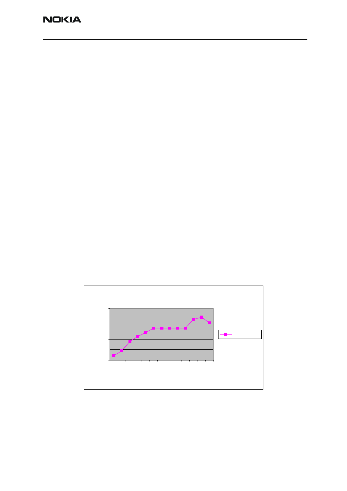
NPE-4
PAMS Technical Documentation 6 - Troubleshooting
Attachment instructions
• ESD Protection Follow RFMD’s ESD Work Instructions when handling microcircuit
devices.
• Before attachment can begin, the modules to be attached MUST BE BAKED in a calibrated oven/chamber for 24 hours at 125ºC to remove moisture from the package.
• Set up the PC board to be attached so that it is directly over the blower section of
the Hako 853 heater. The PC board should be 0.5 inches above the Hako 853.
• Set the Hako 853 heater to 250ºC and the Thermo Flow BGA/SMD blower temperature to 250ºC. The Thermo Flow blower speed should be set to 8. The actual attachment reflow profile is shown at the figure below.
• Turn the Hako 853 ON and preheat the PC board for 2.0 minutes.
• After the 2.0 minutes, set the Hako 853 temperature to 200ºC and continue preheating for another 1.0 minute.
• Using ESD protection and tweezers, carefully place the module to be attached, on
the board. Verify the proper alignment and pin 1 orientation.
• Turn on the blower for the Thermo Flow BGA/SMD blower. Verify that the temperature setting is 250ºC with a blower speed of 8 and then heat the top of the module.
Hold the blower nozzle approximately 0.25 inches from the top of module.
• Module should be solder with in 1 minute.
• Turn OFF the Hako 853 heater and the Thermo flow blower.
• Wait 5 minutes before handling the PC board as it should be close to room temperature at this time.
Atta chment Reflow Profile
250
200
150
100
50
Temperature
0
1
0
3
2
Time
4
6
5
Temper ature
Original ãNokia Corporation. Page 6-51
Page 52

NPE-4
6 - Troubleshooting PAMS Technical Documentation
Phoenix tuning
Before any tuning the phone should syncronised with the PC.
Connect the the phone to a PC with DAU-9P cable and dongle and follow the following
instructions:
Start Phoenix Service Software
Select File Alt-F
Scan Product Ctrl-R
Wait until phone information shows in the lower right corner of the screen.
RF tuning after repairs
Different repairs require different tuning. In general it is necessary to determine in which
section the repair was done to select which tunings to perform. To determine if RF tuning
is necessary after repair it is important that the functionality of the repaired circuit is
understood well.
• In general repairs in the TX part will require "TX Power Level Tuning" and "TX IQ
Tuning".
• In general repairs in the RX part or PLL part always require "RX Calibration" and
in some cases require "RX AM Suppression" tuning, "RX Channel Select Filter Calibration" and/or "RX Band Filter Response Compensation" tuning.
Other parts interfacing to TX, RX or PLL might require tuning, but common sense should
be used, e.g. if a component that has no influence on RF performance has been changed,
e.g. the microphone, on/off key, mechanichal parts or similar, there is no need to do any
RF tuning.
RX Calibration
The "RX calibration" is used to determine gain at different gain-settings for front-end
and Hagar and needs to be done in both bands.
EGSM
Set operating mode to local mode
Select Maintenance Alt-M
Tuning T
RX Calibration C
Wait until the RX Calibration window pops up.
Select Band GSM 900
Autom.- 80
1st Man.- 50
2nd Man.- 85
Page 6-52 ãNokia Corporation. Original
Page 53

NPE-4
PAMS Technical Documentation 6 - Troubleshooting
The setup should now look like this:
Select Automatic, press Start and a new window pops up:
Select default, press OK and the window closes.
Now it is possible to press the calibrate button in the RX Calibration window.
Original ãNokia Corporation. Page 6-53
Page 54

NPE-4
6 - Troubleshooting PAMS Technical Documentation
Press Calibrate and a window pops up:
Connect an external signal generator to the RF connector of the phone and set the generator as told in the window.
Press ok and the window closes.
PCN
Press Stop in the RX Calibration window and a new window pops up:
Press Yes and the EGSM RX Calibration is finished.
Set operating mode to local mode
Select Maintenance Alt-M
Tuning T
RX Calibration C
Wait until the RX Calibration window pops up
Select Band GSM 1800
Autom.- 80
1st Man.- 50
nd
Man.- 85
2
Page 6-54 ãNokia Corporation. Original
Page 55

NPE-4
PAMS Technical Documentation 6 - Troubleshooting
The setup should now look like this:
Select Automatic, press Start and a new window pops up:
Select default, press OK and the window closes.
Now it is possible to press the calibrate button in the RX Calibration window.
Original ãNokia Corporation. Page 6-55
Page 56

NPE-4
6 - Troubleshooting PAMS Technical Documentation
Press Calibrate and a window pops up:
Connect an external signal generator to the RF connector of the phone and set the generator as told in the window.
Press ok and the window closes.
Press Stop in the RX Calibration window and a new window pops up:
Press Yes and the PCN RX Calibration is finished.
RX Band Filter Response Compensation
EGSM
Set operating mode to local mode
Select Maintenance Alt-M
Tuning T
RF Controls F
Wait until the RF Controls window pops up
Select Band GSM 900
Select Maintenance Alt-M
Tuning T
RX Band Filter Response Compensation B
Page 6-56 ãNokia Corporation. Original
Page 57

NPE-4
PAMS Technical Documentation 6 - Troubleshooting
A window pops up:
Select Yes and the RX Band Filter Response Compensation window pops up.
The setup should now look like this:
Select Input Signal Level -80
Original ãNokia Corporation. Page 6-57
Page 58

NPE-4
6 - Troubleshooting PAMS Technical Documentation
Press Manual tuning and a window pops up:
Connect an external signal generator to the RF connector of the phone and set the generator as told in the window.
Press OK and a new window pops up:
PCN
Set the generator as told in the window.
Press OK and a new window pops up. Repeat this sequense 9 times until all channels are
done.
Press Stop, Write to PM Area (In the RX Band Filter Response Compensation window) and
a window pops up:
Press Yes and the EGSM RX Band Filter Response Compensation is finished.
Set operating mode to local mode
Select Maintenance Alt-M
Tuning T
RF Controls F
Page 6-58 ãNokia Corporation. Original
Page 59

NPE-4
PAMS Technical Documentation 6 - Troubleshooting
Wait until the RF Controls window pops up
Select Band GSM 1800
Select Maintenance Alt-M
Tuning T
RX Band Filter Response CompensationB
A window pops up:
Select Yes and the RX Band Filter Response Compensation window pops up.
The setup should now look like this:
Select Input Signal Level -80
Original ãNokia Corporation. Page 6-59
Page 60
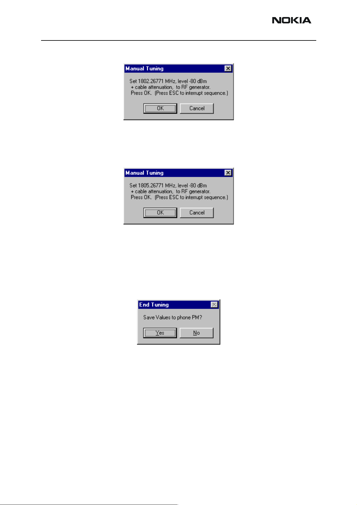
NPE-4
6 - Troubleshooting PAMS Technical Documentation
Press Manual tuning and a window pops up:
Connect an external signal generator to the RF connector of the phone and set the generator as told in the window.
Press OK and a new window pops up:
Set the generator as told in the window.
Press OK and a new window pops up. Repeat this sequense 9 times until all channels are
done.
Press Stop, Write to PM Area (In the RX Band Filter Response Compensation window) and
a window pops up:
Press Yes and the PCN RX Band Filter Response Compensation is finished.
RX Channel Select Filter Calibration
This calibration is calibrating the Baseband filter inside Hagar, for this reason the calibration is not done in both bands.
Set operating mode to local mode
Select Maintenance Alt-M
Tuning T
RX Channel Select filter Calibration H
Page 6-60 ãNokia Corporation. Original
Page 61
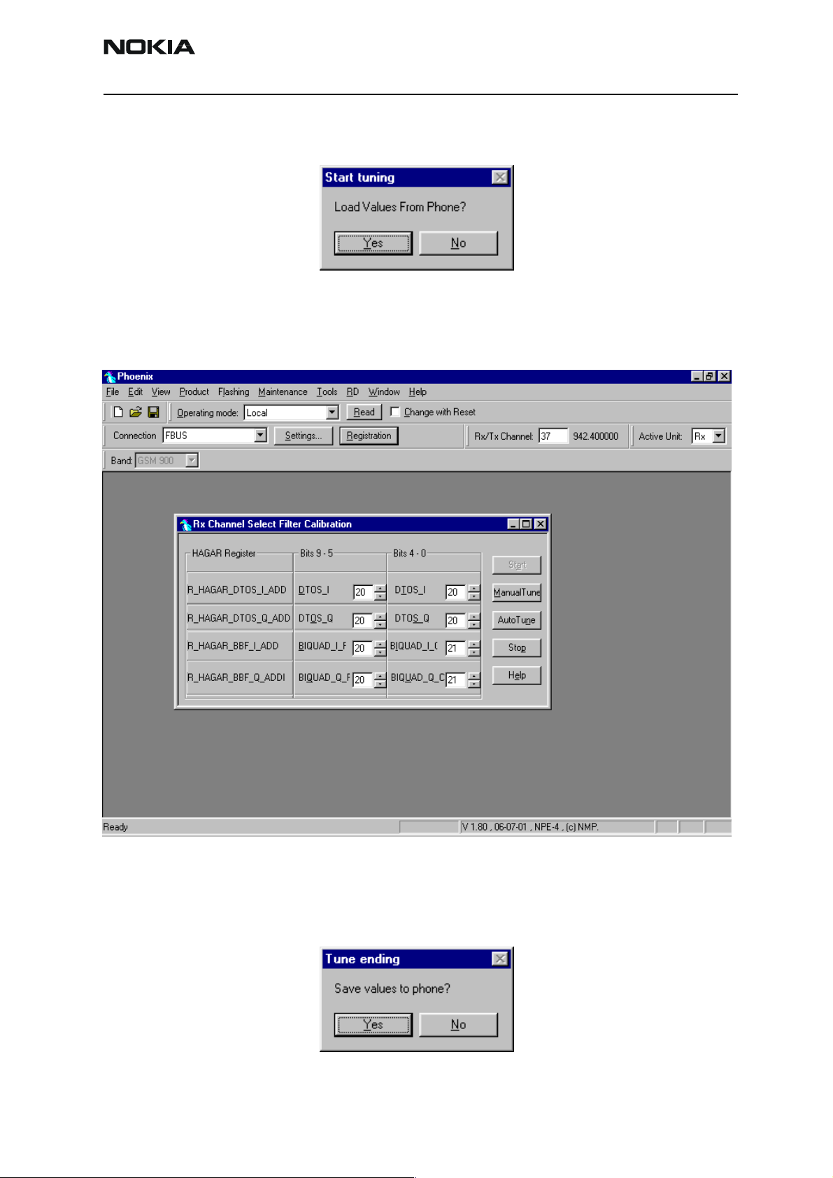
NPE-4
PAMS Technical Documentation 6 - Troubleshooting
A window pops up:
Select Yes and the RX Channel Select Filter Calibration window pops up.
The setup should now look like this:
Press Autotune and the optimal values are found.
Press Stop and a new window pops up:
Original ãNokia Corporation. Page 6-61
Page 62

NPE-4
6 - Troubleshooting PAMS Technical Documentation
Press Yes and the RX Channel Select Filter Calibration is finished.
RX AM Suppression
This calibration is tuning the AM suppression performance of Hagar mixers and will have
to be done in both bands. If flash or Hagar have been replaced or Full Factory settings
have been performed RX AM Suppression must be done.
EGSM
Set operating mode to local mode
Select Maintenance Alt-M
Tuning T
RX AM Suppression S
Wait until the RX AM Suppression window pops up
Select Band GSM 900
Press Start and a window pops up:
Page 6-62 ãNokia Corporation. Original
Page 63
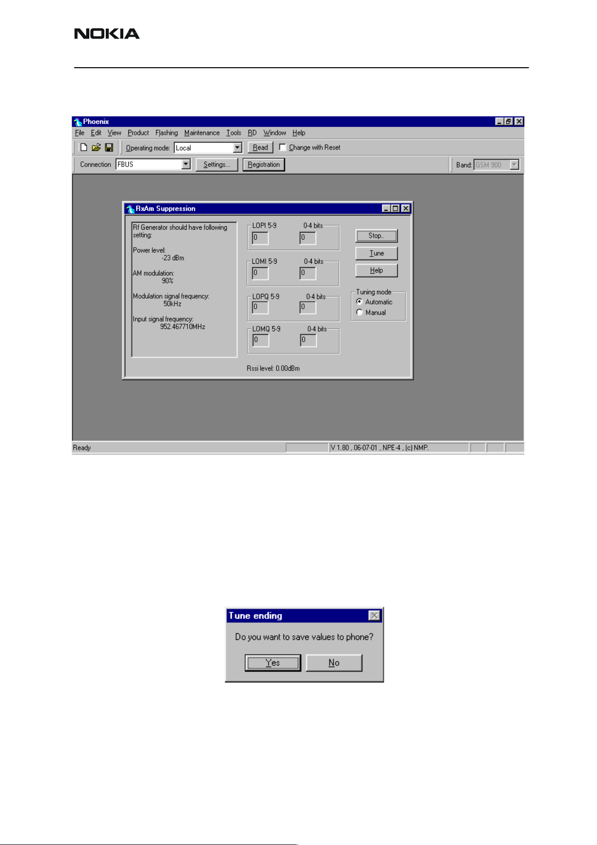
NPE-4
PAMS Technical Documentation 6 - Troubleshooting
Select Default, press OK and the setup should now look like this:
PCN
Connect an external signal generator to the RF connector of the phone and set the generator as told in the window.
Select Tuning mode Automatic
Press Tune and the optimal values are found.
Press Stop and a window pops up:
Press Yes and the EGSM RX AM Suppression tuning is finished.
Set operating mode to local mode
Original ãNokia Corporation. Page 6-63
Page 64

NPE-4
6 - Troubleshooting PAMS Technical Documentation
Select Maintenance Alt-M
Tuning T
RX AM Suppression S
Wait until the RX AM Suppression window pops up
Select Band GSM 1800
Press Start and a window pops up:
Select Default, press OK and the setup should now look like this:
Connect an external signal generator to the RF connector of the phone and set the generator as told in the window.
Page 6-64 ãNokia Corporation. Original
Page 65

NPE-4
PAMS Technical Documentation 6 - Troubleshooting
Select Tuning mode Automatic
Press Tune and the optimal values are found.
Press Stop and a window pops up:
Press Yes and the PCN RX AM Suppression tuning is finished.
TX Power tuning
This tuning must be done in both bands.
Note: TX Power tuning must be done with a peak power meter, e.g. Rohde & Schwarz model
NRVD with a Rohde & Schwarz Peak Power Sensor TDMA Model NRV-Z31 and a suitable
attenuator.
The use of power meter in GSM testers is likely to cause larger error than the use of a
dedicated power meter and might cause the phone to be non-compliant with GSM specifications.
EGSM
Set operating mode to local mode
Select Maintenance Alt-M
Tuning T
TX Power Level Tuning L
Wait until the TX Power Level Tuning window pops up.
Connect a calibrated powermeter to the RF connector of the phone.
Select Band GSM 900
Active Unit TX
Original ãNokia Corporation. Page 6-65
Page 66

NPE-4
6 - Troubleshooting PAMS Technical Documentation
Press Start and a window pops up:
Select Permanent memory, press OK and the window closes.
Select TX Data Type Random
The setup should now look like this:
Select TX PA Mode High
Adjust DAC Values for Power Level 5, 15 and 19 according to Target values.
Press calculate, check if all levels match the target values, correct if necessary.
Select TX PA Mode Low
Page 6-66 ãNokia Corporation. Original
Page 67

NPE-4
PAMS Technical Documentation 6 - Troubleshooting
Adjust DAC Values for Power Level 7, 15 and 19 according to Target values.
Press calculate, check if all levels match the target values, correct if necessary.
Press Stop and a window pops up:
Select 'Save values to Phone Permanent Memory'
PCN
Press Yes and the EGSM TX Power Level Tuning is finished.
Set operating mode to local mode
Select Maintenance Alt-M
Tuning T
TX Power Level Tuning L
Wait until the TX Power Level Tuning window pops up.
Connect a calibrated powermeter to the RF connector of the phone.
Select Band GSM 1800
Active Unit TX
Press Start and a window pops up:
Select Permanent memory, press OK and the window closes.
Select TX Data Type Random
Original ãNokia Corporation. Page 6-67
Page 68

NPE-4
6 - Troubleshooting PAMS Technical Documentation
The setup should now look like this:
Select TX PA Mode High
Adjust DAC Values for Power Level 0, 11 and 15 according to Target values.
Press calculate, check if all levels match the target values, correct if necessary.
Press Stop and a window pops up:
Select 'Save values to Phone Permanent Memory'
Press Yes and the EGSM TX Power Level Tuning is finished.
Page 6-68 ãNokia Corporation. Original
Page 69

NPE-4
PAMS Technical Documentation 6 - Troubleshooting
TX I/Q Tuning
This tuning must be done in both bands.
EGSM
Set operating mode to local mode
Select Maintenance Alt-M
Tuning T
TX IQ Tuning I
Wait until the TX IQ Tuning window pops up.
Connect a Spectrum Analyzer or GSM tester with the option *Narrow Spectrum' to the
RF connector of the phone.
If a spectrum analyzer is used then use the following settings.
EGSM
Center Frequency 897.4 MHz
Frequency Span 300 kHz
Resolution Bandwidth 3kHz
Video Bandwidth 3kHz
Sweep Time 3 sek.
Sweep Type Clear/Write
Detector Type Max Peak
Reference level 35 dBm
Marker 1 897.33229 MHz
Marker 2 897.4 MHz
Marker 3 897.46771 MHz
Use an appropriate attenuator 10 or 20dB insertion loss and set the Reference Level Offset according to insertion loss from the phone to the Spectrum Analyzer.
Select Band GSM 900
Operation Mode Burst
RX/TX Channel 37
Select 'Load from Product'
Press Start
Select TX Data Type All1
Original ãNokia Corporation. Page 6-69
Page 70

NPE-4
6 - Troubleshooting PAMS Technical Documentation
TX PA Mode Free
The setup should now look like this:
Page 6-70 ãNokia Corporation. Original
Page 71

NPE-4
PAMS Technical Documentation 6 - Troubleshooting
The Spectrum Analyzer now shows a plot like this:
The purpose of this tuning is to tune the carrier signal and the +67kHz signal to a minimum level (Marker 2 and 3).
Use the varables 'TX I DC offset' and 'TX Q DC offset' to adjust the carrier signal to a minimum level (Marker 2).
Original ãNokia Corporation. Page 6-71
Page 72

NPE-4
6 - Troubleshooting PAMS Technical Documentation
The Spectrum Analyzer now shows a plot like this:
Use the varables 'Amplitude difference' and 'Phase difference' to adjust the +67kHz signal to a minimum level (Marker 3).
Page 6-72 ãNokia Corporation. Original
Page 73
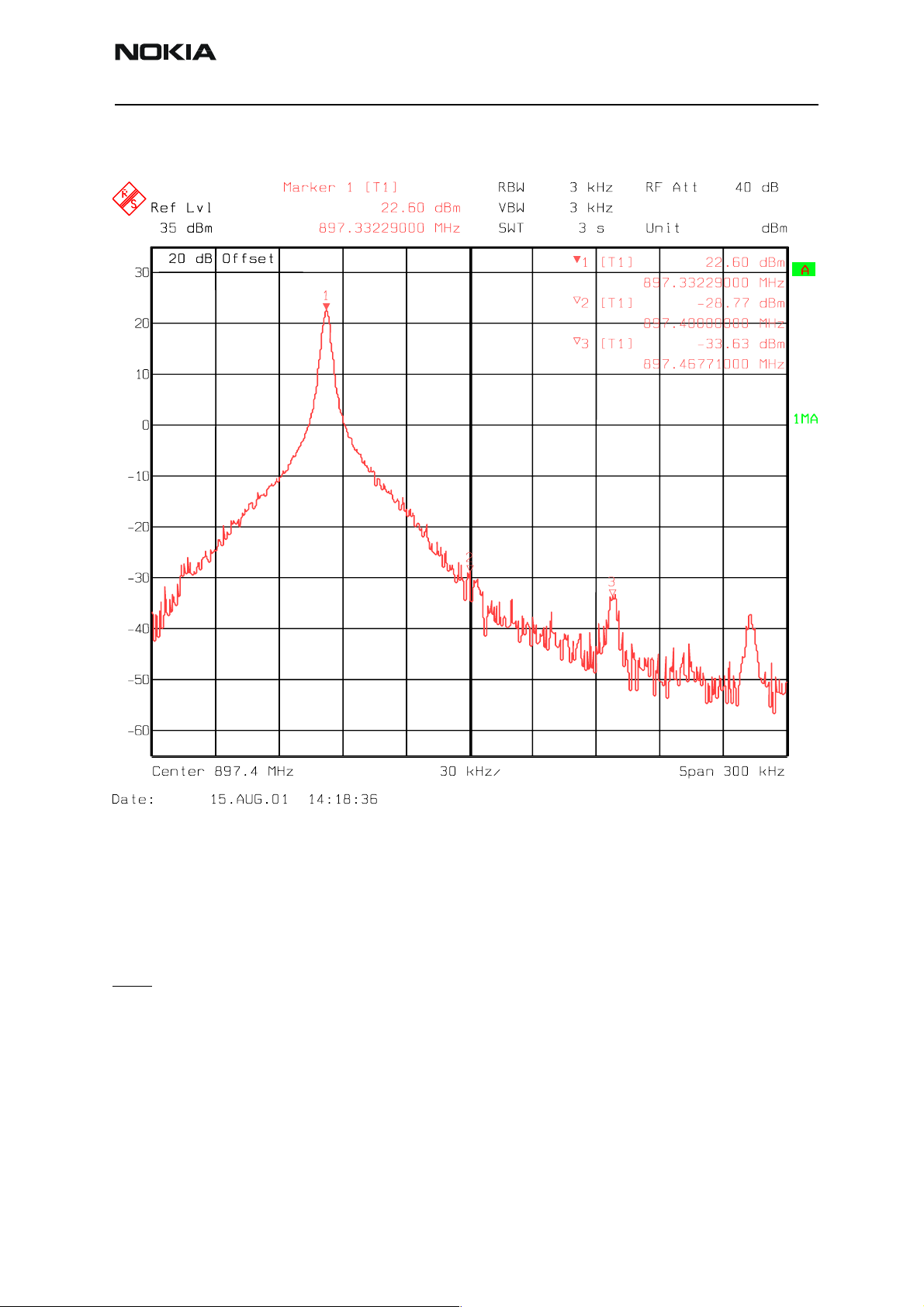
NPE-4
PAMS Technical Documentation 6 - Troubleshooting
The Spectrum Analyzer now shows a plot like this:
Select 'Save to Product'
Press Stop and the values are stored in the phone.
The EGSM TX IQ Tuning is now finished.
Note:
PCN
Original ãNokia Corporation. Page 6-73
The optimal values for "TX I and Q Offset" and "Amplitude and Phase Difference" vary
from phone to phone.
Set operating mode to local mode
Select Maintenance Alt-M
Tuning T
TX IQ Tuning I
Page 74

NPE-4
6 - Troubleshooting PAMS Technical Documentation
Wait until the TX IQ Tuning window pops up.
Connect a Spectrum Analyzer or GSM tester with the option *Narrow Spectrum' to the
RF connector of the phone.
If a spectrum analyzer is used then use the following settings.
PCN
Center Frequency 1747.8MHz
Frequency Span 300 kHz
Resolution Bandwidth 3 kHz
Video Bandwidth 3 kHz
Sweep Time 3 sek.
Sweep Type Clear/Write
Detector Type Max Peak
Reference level 35 dBm
Marker 1 1747.73229 MHz
Marker 2 1747.8 MHz
Marker 3 1747.86771 MHz
Use an appropriate attenuator 10 or 20dB insertion loss and set the Reference Level Offset according to insertion loss from the phone to the Spectrum Analyzer.
Select Band GSM 1800
Operation Mode Burst
RX/TX Channel 700
Select 'Load from Product'
Press Start
Select TX Data Type All1
TX PA Mode Free
Page 6-74 ãNokia Corporation. Original
Page 75

NPE-4
PAMS Technical Documentation 6 - Troubleshooting
The setup should now look like this:
Original ãNokia Corporation. Page 6-75
Page 76
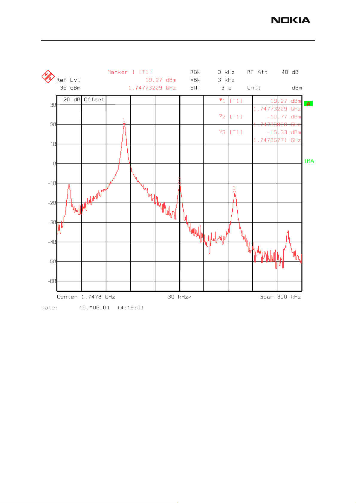
NPE-4
6 - Troubleshooting PAMS Technical Documentation
The Spectrum Analyzer now shows a plot like this:
The purpose of this tuning is to tune the carrier signal and the +67kHz signal to a minimum level (Marker 2 and 3).
Use the varables 'TX I DC offset' and 'TX Q DC offset' to adjust the carrier signal to a minimum level (Marker 2).
Page 6-76 ãNokia Corporation. Original
Page 77
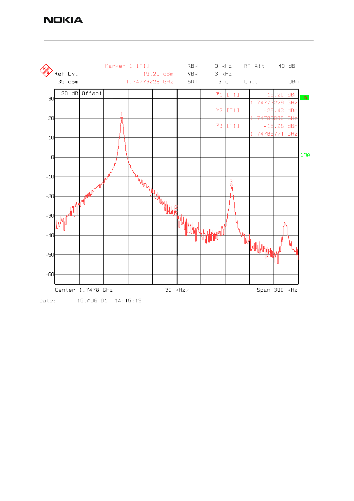
NPE-4
PAMS Technical Documentation 6 - Troubleshooting
The Spectrum Analyzer now shows a plot like this:
Use the varables 'Amplitude difference' and 'Phase difference' to adjust the +67kHz signal to a minimum level (Marker 3).
Original ãNokia Corporation. Page 6-77
Page 78
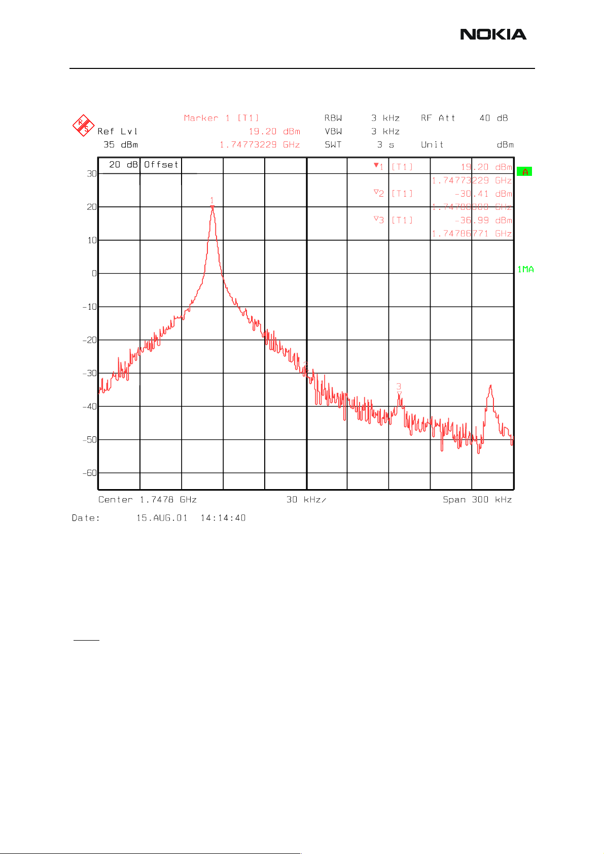
NPE-4
6 - Troubleshooting PAMS Technical Documentation
The Spectrum Analyzer now shows a plot like this:
Select 'Save to Product'
Press Stop and the values are stored in the phone.
The PCN TX IQ Tuning is now finished.
Note:
Page 6-78 ãNokia Corporation. Original
The optimal values for "TX I and Q Offset" and "Amplitude and Phase Difference" vary
from phone to phone.
 Loading...