

Page 1

Nokia Customer Care
6255/6255i6256/6256i (RM-19)
Mobile Terminal
Baseband Description and
Troubleshooting
Issue 2 05/2005 Company Confidential ©2005 Nokia Corporation
Page 2

6255/6255i6256/6256i (RM-19)
Baseband Description and Troubleshooting Nokia Customer Care
Contents Page
Introduction ..................................................................................................................................................... 4
Power Up and Reset ....................................................................................................................................6
Power Up - Power Key............................................................................................................................. 8
Power Up - Charger Connection .......................................................................................................... 8
Power Up - RTC Alarm............................................................................................................................. 9
Power Off .......................................................................................................................................................9
Power Consumption and Operation Modes .........................................................................................9
Power-off Mode........................................................................................................................................ 9
Sleep Mode.............................................................................................................................................. 10
Active Mode ............................................................................................................................................ 10
Charging Mode....................................................................................................................................... 10
Power Distribution ....................................................................................................................................11
Clock Distribution ......................................................................................................................................13
RFClk (19.2MHz Analog)...................................................................................................................... 13
RFConvClk (19.2MHz Digital)............................................................................................................. 14
CBUSClk Interface ................................................................................................................................. 15
DBUS Clk Interface................................................................................................................................ 16
SleepCLK (Digital) .................................................................................................................................. 17
SleepCLK (Analog).................................................................................................................................. 18
Flash Programming ...................................................................................................................................18
Connections to Baseband.................................................................................................................... 18
Baseband Power Up .............................................................................................................................. 18
Flash Programming Indication........................................................................................................... 19
Flashing..................................................................................................................................................... 19
Flash Programming Error Codes ........................................................................................................ 22
Charging Operation ...................................................................................................................................24
Battery ...................................................................................................................................................... 24
Charging Circuitry ................................................................................................................................. 24
Charger Detection.................................................................................................................................. 25
Audio .............................................................................................................................................................25
Displays and Keymat ................................................................................................................................25
Main Display............................................................................................................................................ 26
Secondary Display.................................................................................................................................. 27
Keymat...................................................................................................................................................... 27
Camera .........................................................................................................................................................27
DC Measurements.................................................................................................................................. 28
AC Measurements.................................................................................................................................. 28
FM Radio ......................................................................................................................................................29
FM Radio Test ......................................................................................................................................... 29
USB Interface ..............................................................................................................................................31
Accessories ..................................................................................................................................................33
Charging.......................................................................................................................
Pop-port Headset Detection............................................................................................................... 36
FBus Detection........................................................................................................................................ 36
Accessory Detection Through ACI..................................................................................................... 37
RUIM (SIM CAR) ........................................................................................................................................39
Main Display Test Points ........................................................................................................................... 40
............................ 34
Page 2 ©2005 Nokia Corporation Company Confidential Issue 2 05/2005
Page 3

6255/6255i6256/6256i (RM-19)
Nokia Customer Care Baseband Description and Troubleshooting
Secondary Display Test Points.................................................................................................................. 45
GPS Module .................................................................................................................................................48
Troubleshooting............................................................................................................................................ 49
Mobile Terminal is Totally Dead ............................................................................................................50
Flash Programming Does Not Work .....................................................................................................51
Power Does Not Stay on or the Mobile Terminal is Jammed ........................................................53
Charger Faults ............................................................................................................................................55
Audio Faults ................................................................................................................................................56
Earpiece .................................................................................................................................................... 56
Microphone ............................................................................................................................................. 57
IHF.............................................................................................................................................................. 58
Vibra .......................................................................................................................................................... 59
Display Faults ..............................................................................................................................................60
Main Display............................................................................................................................................ 60
Secondary Display.................................................................................................................................. 62
Keypad Faults .............................................................................................................................................63
Power Key ................................................................................................................................................ 63
UI Modules............................................................................................................................................... 64
EL Panel and Driver ............................................................................................................................... 65
USB ................................................................................................................................................................66
MMC ..............................................................................................................................................................70
FM Radio ......................................................................................................................................................71
Camera .........................................................................................................................................................73
Bluetooth .....................................................................................................................................................73
SIM ................................................................................................................................................................73
GPS ................................................................................................................................................................75
Issue 2 05/2005 ©2005 Nokia Corporation Company Confidential Page 3
Page 4

6255/6255i6256/6256i (RM-19)
Baseband Description and Troubleshooting Nokia Customer Care
This page intentionally left blank.
Page 4 ©2005 Nokia Corporation Company Confidential Issue 2 05/2005
Page 5

6255/6255i6256/6256i (RM-19)
Nokia Customer Care Baseband Description and Troubleshooting
Introduction
The 6255/6255i/6256/6256i baseband module is a tri-mode, Code Division Multiple
Access (CDMA), dual-band engine and is based on the DCT4.5 standard. The baseband
engine includes two major Application Specific Integrated Circuits (ASICs):
• D2200 — Universal Energy Management Enhanced Integrated Circuit (UEME IC),
which includes the audio circuits, charge control, and voltage regulators
• D2800 — Main phone processor, which includes system logic for CDMA, two
Digital Signal Processors (DSPs), the Main Control Unit (MCU), and the memory
The BL-6C Li-ion battery is used as the main power source and has a nominal capacity of
1070 mA/h.
Issue 2 05/2005 ©2005 Nokia Corporation Company Confidential Page 5
Page 6

6255/6255i6256/6256i (RM-19)
Baseband Description and Troubleshooting Nokia Customer Care
Battery
UHS Jack
DC Jack
Tomahawk
Antenna
Bluetooth
GPS
FM Radio
Zocus
Nut
USB
CBUS
PCM / UART
UART
19.2 MHz
VIO
Production
Test IF
UEME
RF
Tiku EDGE
Sim
Regulation
Charge Control
Audio
FBUS / MBUS
SIM I/F
RTC
D
B
U
S
MCU ARM925
PDRAM
MMC
32 KHz
Amplifier
PWM
PWM
Parallel
Serial
Regulator
Mic
IHF Speaker
EarPiece
Vibra
Disp BL’s
Cam Flash
Int Display
Ext Display
Flash Memory
(Program,
NOR)
SDRAM
Flash Memory
(User, NAND)
VCORE
SMPS
C-DSP Lead3
A-DSP Lead 3
2G System Logic
Figure 1: Baseband block diagram
Keyboard
EL
Camera
IRDA
Page 6 ©2005 Nokia Corporation Company Confidential Issue 2 05/2005
Page 7

6255/6255i6256/6256i (RM-19)
Nokia Customer Care Baseband Description and Troubleshooting
Power Up and Reset
The UEME ASIC controls the power up and resets. The baseband can be powered up in
the following ways:
• Pressing the Power button, which means grounding the PWRONX pin of the
UEME
• Connecting the charger to the charger input
• Initiating the Real-time Clock (RTC) alarm, when the RTC logic has been
programmed to give an alarm
After receiving one of the above signals (see Figure 2), the UEME counts a 20ms delay
and then enters reset mode. The watchdog and VCORE start, and if the battery voltage
(VBAT) is greater than Vcoff+, a 200ms delay is started to allow references to settle.
After this delay elapses, the VFLASH1 regulator is enabled. Then, 500us later, VR3, VANA,
and VIO are enabled. Finally, the Power Up Reset (PURX) line is held low for 20ms. This
reset (PURX) is fed to the baseband D2800 processor ASIC, which in turn generates resets
for the MCU and the DSP. During this reset phase, the UEME forces the Voltage
Controlled Temperature Controlled Oscillator (VCTCXO) regulator on regardless of the
status of the sleep control input signal to the UEME.
The FLSRSTx from the UEME is used to reset the flash during power up and to put the
flash in power down during sleep mode. All baseband regulators are switched on when
the UEME is powered on.
The UEME internal watchdogs are running during the UEME reset state, with the longest
watchdog time selected. If the watchdog expires, the UEME returns to the power off
state. The UEME watchdogs are internally acknowledged at the rising edge of the PURX
signal to always give the same watchdog response time to the MCU.
The following timing diagram represents the UEME start-up sequence from reset to
power-on mode.
Issue 2 05/2005 ©2005 Nokia Corporation Company Confidential Page 7
Page 8

6255/6255i6256/6256i (RM-19)
Baseband Description and Troubleshooting Nokia Customer Care
Reference signal
PwrOnX
Charger Detection
RTC
UEMRSTX
VCORE
VFlash1
VIO
VANA
VR3
19.2MHz Clk
PURX
Reset mode is entered and
the watchdog starts
End of settling time (only if Vbat > Vcoff+_);
VFLASH1 regulator enabled
VR3, VANA, VIO, and VCORE enabled;
PURX held LOW
D2800 processor, MCU, and DSP are
reset; VCTCXO regulator forced on
Sleep Clock
t1 t2 t4t3
t1 = 20ms
t2 = 200ms
t3 = 500us
t4 = 20ms
Figure 2: Power-on sequence and timing
Page 8 ©2005 Nokia Corporation Company Confidential Issue 2 05/2005
Page 9

6255/6255i6256/6256i (RM-19)
Nokia Customer Care Baseband Description and Troubleshooting
Figure 3: Measured power-on sequence and timing
Power Up - Power Key
When the power key is pressed, the UEME enters the power-up sequence. Pressing the
power key grounds the PWRONX pin on the UEME. The UEME PWRONX signal is not part
of the keypad matrix. The power key is only connected to the UEME. When the power key
is pressed, an interrupt is generated to the D2800 processor that starts the MCU. The
MCU then reads the UEME interrupt register through the UEME control bus (CBUS) and
notices that it is a PWRONX interrupt. If the PWRONX signal stays low for a certain time,
the MCU accepts this as a valid power-on state and continues with the SW initialization
of the baseband. If the power key does not indicate a valid power-on situation, the MCU
powers off the baseband.
Power Up - Charger Connection
In order to be able to detect and start charging in cases where the main battery is fully
discharged (empty), charging is controlled by start-up charging circuitry.
The VBAT voltage level is monitored by the Charge Control Block (CHACON) inside the
UEME. When the VBAT level is detected to be below the master reset threshold (V
charging starts. Connecting a charger forces the Charging Voltage (VCHAR) input to rise
above the charger detection threshold (VCH
). This causes the UEME to generate
DET+
MSTR-
),
Issue 2 05/2005 ©2005 Nokia Corporation Company Confidential Page 9
Page 10
6255/6255i6256/6256i (RM-19)
Baseband Description and Troubleshooting Nokia Customer Care
100mA of constant output current from the connected charger’s output voltage. The
battery’s voltage rises at it charges, and when the VBAT voltage level is detected to be
higher than master reset threshold limit (V
), the start-up charge is terminated.
MSTR+
When VBAT is greater than V
internal to the UEME, is set to a Logic 1. This causes the UEME RESET block to enter into
its reset sequence.
If the VBAT is detected to fall below V
cancelled. Charging is restarted when a new rising edge on the VCHAR input is detected
(VCHAR rising above VCH
Condition Result
VBAT < V
VBAT < V
VCHAR > VCH
VBAT > V
(start-up charging) Charging starts (VCHAR level begins to rise)
MSTR-
MSTR-
DET+
MSTR+
Power Up - RTC Alarm
If the mobile terminal is in power-off mode when the RTC alarm activates, a wake-up
procedure occurs. After the baseband is powered on, an interrupt is given to the MCU.
When the RTC alarm occurs during active mode, an interrupt is generated to the MCU.
, the Master Output Reset (MSTRX) signal, which is
MSTR+
during start-up charging, charging is
MSTR-
).
DET+
Table 1: Power-up Sequence through Charger Detection
(during charging) Charging is cancelled. A new rising edge of VCHAR
(VCHAR > VCH
Battery charges (VCHAR is rising)
Charging ends. MSTRX is set high and the UEME resets.
) is required to restart charging
DET+
Power Off
The baseband switches to power-off mode if any of following occurs:
• Power key is pressed
• Battery voltage is too low (VBATT < 3.2V)
• Watchdog timer register expires
The UEME controls the power-down procedure.
Power Consumption and Operation Modes
Power-off Mode
During power-off mode, the power (VBAT) is supplied to the D2800 processor, UEME,
MMC, vibra, LED, PA, and PA drivers. During power-off mode, the UEME leakage current
consumption is approximately 40uA + 15uA from ZOCOS.
Page 10 ©2005 Nokia Corporation Company Confidential Issue 2 05/2005
Page 11

6255/6255i6256/6256i (RM-19)
Nokia Customer Care Baseband Description and Troubleshooting
Sleep Mode
When the SLEEPX signal is detected low by the UEME, the mobile terminal enters sleep
mode. In sleep mode, both processors (MCU and DSP) are in stand-by mode. The mobile
terminal enters sleep mode only when both processors make this request. The following
processes occur during sleep mode:
• VIO and VFLASH1 regulators are put into low quiescent current mode
• VCORE enters LDO mode
• VANA and VFLASH2 regulators are disabled
• All RF regulators are disabled
• VCTCXO (19.2MHz clock) is shut down
• 32kHz sleep clock oscillator is used as the baseband reference clock
The average current consumption of the mobile terminal in this mode can vary
depending on the software state (e.g., slot cycle 0,1, or 2, and if the mobile terminal is
working on IS95 or IS2000 for CDMA). However, on average the current consumption is
about 1.3mA in sleep mode and 100mA in active mode.
Sleep mode is exited either by the expiration of a sleep clock counter in the UEME or by
some external interrupt (e.g., charger connection, key press, headset connection). Any of
these conditions cause a high SLEEPX signal, which is detected by the UEME, and causes
the mobile terminal to enter active mode where all functions are activated.
Active Mode
During active mode, the mobile terminal is in normal operation, scanning for channels,
listening to a base station, transmitting and processing information. There are several
sub-states in the active mode depending on the mobile terminal present state of the
mobile terminal, such as burst reception, burst transmission, if the DSP is working, etc.
In active mode, software controls the UEME radio frequency (RF) regulators (VR1A and
VR1B), which can be enabled or disabled. These regulators work via the UEME charge
pump. VSIM can be enabled or disabled, and its output voltage can be programmed to be
1.8V or 3.0V. VR2 and VR4—VR7 can be enabled, disabled, or forced into low quiescent
current mode. VR3 is always enabled in active mode, disabled during sleep mode, and
cannot be controlled by the software in the same way as the other regulators. VR3 only
turns off if both processors (DSP and MCU) request to be in sleep mode.
Charging Mode
Charging mode can be performed in parallel with any other operating mode. A BSI
resistor inside the battery indicates the battery type and size and corresponds to a
specific battery capacity.
The battery voltage, temperature, size, and charging current are measured by the UEME
and controlled by the Energy Management (EM) charging algorithm.
Issue 2 05/2005 ©2005 Nokia Corporation Company Confidential Page 11
Page 12

6255/6255i6256/6256i (RM-19)
Baseband Description and Troubleshooting Nokia Customer Care
The charging control circuitry (CHACON) inside the UEME controls the charging current
delivered from the charger to the battery. The battery voltage rise is limited by turning
the UEME switch off when the battery voltage has reached 4.2V. The charging current is
monitored by measuring the voltage drop across a 220mOhm resistor.
Power Distribution
In normal operation, the baseband is powered from the mobile terminal‘s battery. The
battery consists of one Lithium-Ion cell capacity of 1070 mAh and some safety and
protection circuits to prevent harm to the battery.
The UEME ASIC controls the power distribution to the entire mobile terminal through the
BB and RF regulators. The battery feeds power directly to the following parts of the
system:
•UEME
•PA
•Vibra
• Display lights
• Keyboard lights
The heart of the power distribution to the mobile terminal is the UEME. The UEME
includes all the voltage regulators and feeds the power to the system. The UEME handles
hardware power-up functions so the regulators are not powered and the power-up reset
(PURX) is not released if the battery voltage is less than 2.8V.
The baseband is powered from five different UEME regulators (see Table 2):
Table 2: Baseband Regulators
Regulator
VCORE
DC/DC
VIO 150 1.8 Enabled always except during power-off mode
VFLASH1 70 2.78 Enabled always except during power-off mode
Maximum
Current (mA)
300 1.35 The power-up default value is 1.35V. The output voltage is
Vout (V) Notes
selectable: 1.0V/1.3V/1.5V/1.8V.
(Note: If using D2800 processor version 1, the default is
1.57V.)
VFLASH2 40 2.78 Enabled only when data cable is connected
VANA 80 2.78 Enabled only when the system is awake (off during sleep and
power-off modes)
VSIM 25 3.0 Enabled during power-up mode and scanning for a SIM card
Page 12 ©2005 Nokia Corporation Company Confidential Issue 2 05/2005
Page 13

6255/6255i6256/6256i (RM-19)
Nokia Customer Care Baseband Description and Troubleshooting
Table 3 includes the UEME RF regulators.
Table 3: RF Regulators
Regulator
VR1A 10 4.75 Enabled when cell receiver is on
VR1B 10 4.75 Enabled when the transmitter is on
VR2 100 2.78 Enabled when the transmitter is on
VR3 20 2.78 Enabled when SleepX is high
VR4 50 2.78 Enabled when the receiver is on
VR5 50 2.78 Enabled when the receiver is on
VR6 50 2.78 Enabled when the transmitter is on
VR7 45 2.78 Enabled when the receiver is on
Maximum
Current (mA)
Vout (V) Notes
The charge pump that is used by VR1A is constructed around the UEME. The charge
pump works with the 1.2MHz clock (CBUS) oscillator and gives a 4.75V regulated output
voltage to the RF.
Issue 2 05/2005 ©2005 Nokia Corporation Company Confidential Page 13
Page 14

6255/6255i6256/6256i (RM-19)
Baseband Description and Troubleshooting Nokia Customer Care
Clock Distribution
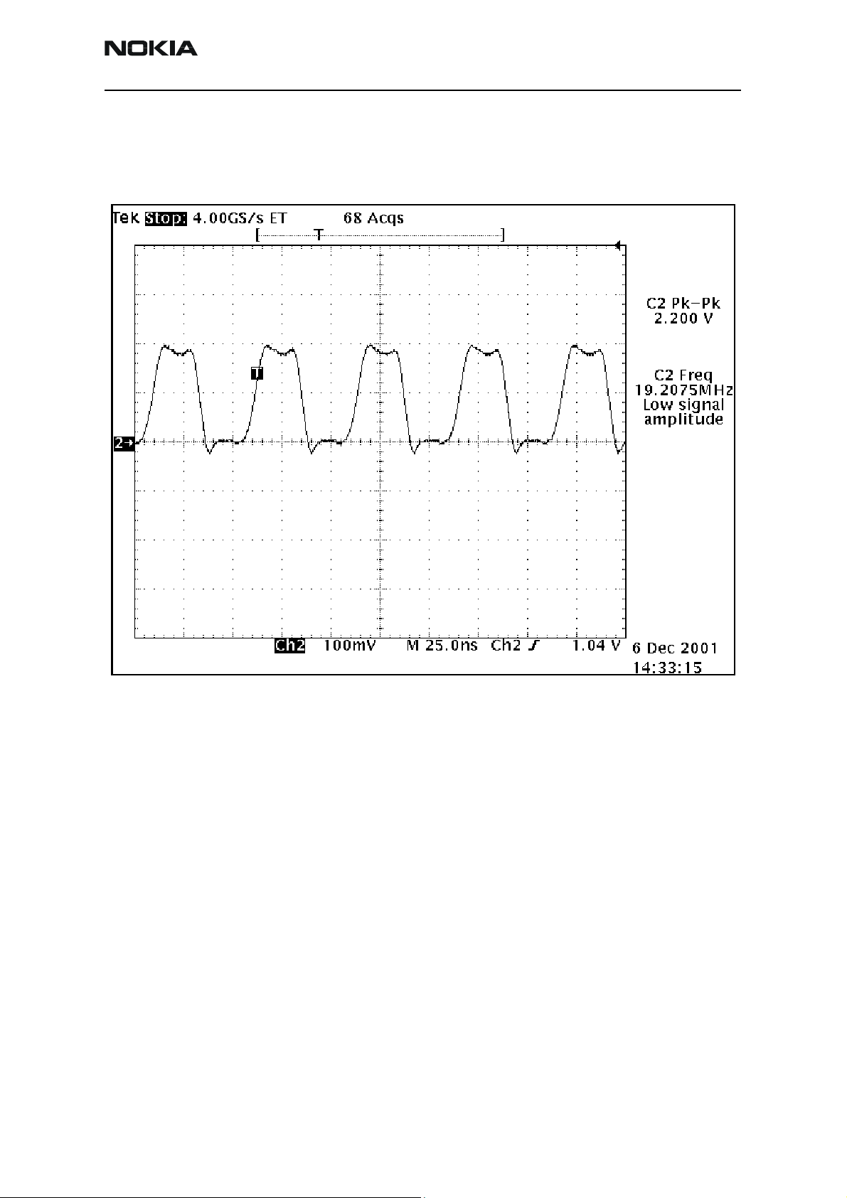
RFClk (19.2MHz Analog)
The main clock signal for the baseband is generated from the voltage-controlled
temperature-controlled crystal oscillator (VCTCXO). This 19.2MHz clock signal is
generated by the radio frequency circuitry and fed to the radio frequency clock (RFCLK)
pin of the D2800 processor. The 19.2MHz clock can be stopped during sleep mode by
disabling the UEME regulator output (VR3), which in turn powers off the VCTCXO.
Figure 4: Waveform of the 19.2MHz clock (VCTCXO)
Page 14 ©2005 Nokia Corporation Company Confidential Issue 2 05/2005
Page 15
6255/6255i6256/6256i (RM-19)
Nokia Customer Care Baseband Description and Troubleshooting
RFConvClk (19.2MHz Digital)
The D2800 processor distributes the 19.2MHz clock to the internal processors (the DSP
and MCU) where the software multiplies this clock by seven (=134.4MHz) for the DSP
and by two (=38.4MHz) for the MCU.
Figure 5: RFCovCLk waveform
Issue 2 05/2005 ©2005 Nokia Corporation Company Confidential Page 15
Page 16
6255/6255i6256/6256i (RM-19)
Baseband Description and Troubleshooting Nokia Customer Care
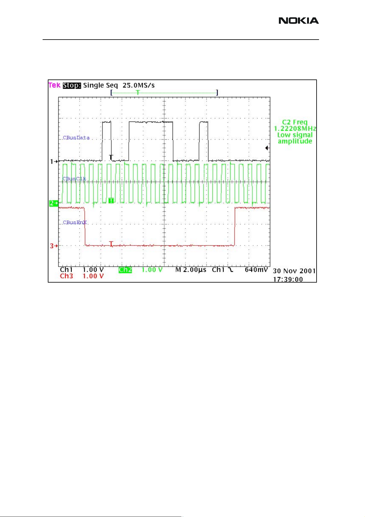
CBUSClk Interface
CBUS utilizes a 1.2MHz clock signal, which is used by the MCU to transfer data between
the UEME and the D2800 processor.
Figure 6: CBUS data transfer
Page 16 ©2005 Nokia Corporation Company Confidential Issue 2 05/2005
Page 17

6255/6255i6256/6256i (RM-19)
Nokia Customer Care Baseband Description and Troubleshooting
DBUS Clk Interface
DBUS utilizes a 9.6MHz clock signal, which is used by the DSP to transfer data between
the UEME and the D2800 processor.
Figure 7: DBUS data transfer
Issue 2 05/2005 ©2005 Nokia Corporation Company Confidential Page 17
Page 18

6255/6255i6256/6256i (RM-19)
Baseband Description and Troubleshooting Nokia Customer Care
SleepCLK (Digital)
The UEME provides a 32kHz sleep clock for internal use and also to the D2800 processor,
where it is used for the sleep-mode timing.
Figure 8: 32 kHz Digital output from UEME
Page 18 ©2005 Nokia Corporation Company Confidential Issue 2 05/2005
Page 19

6255/6255i6256/6256i (RM-19)
Nokia Customer Care Baseband Description and Troubleshooting
SleepCLK (Analog)
When the system enters sleep mode or power-off mode, the external 32KHz crystal
provides a reference to the UEME. The RTC circuit also uses this clock to turn on the
mobile terminal during power-off or sleep mode.
Figure 9: 32KHz analog waveform at 32KHz crystal input
Flash Programming
Connections to Baseband
The flash programming equipment is connected to the baseband using test pads for
galvanic connection. The test pads are allocated in such a way that they can be accessed
when the mobile terminal is already assembled. The flash programming interface
includes the VPP, FBUSTX, FBUSRX, MBUS, and BSI signals, which are used by the FLS-8
for flashing. The connection is through the UEME, which means that the logic voltage
levels of these signals correspond to 2.78V. Power is supplied to the mobile terminal
using the battery contacts.
Baseband Power Up
The baseband power is controlled by the flash prommer in production and in
re-programming situations. The baseband powers up by applying supply voltage to the
battery terminals. After the baseband is powered up, flash programming indication
begins (see the following "Flash Programming Indication" section).
Issue 2 05/2005 ©2005 Nokia Corporation Company Confidential Page 19
Page 20

6255/6255i6256/6256i (RM-19)
Baseband Description and Troubleshooting Nokia Customer Care
Flash Programming Indication
After connecting the flash prommer to the mobile terminal, the flash prommer sets the
MBUS line low to notify the MCU that the flash prommer is connected. This causes the
UEME reset state machine to perform a reset to the system by setting the PURX signal
low for 20ms.
During flash programming, the MBUS signal transmitted from the UEME to the flash
prommer is used as the clock for synchronous communication. This MBUS clock is also
supplied by the UEME to the D2800 processor, along with the MBUSRX signal. If the
MBUSRX signal is low, the MCU enters flash programming mode. To avoid accidental
entry into flash-programming mode, the MCU waits to get input data from the flash
prommer. If the timer expires without any data being received, the MCU continues the
boot sequence.
When the mobile terminal has entered flash programming mode, the flash prommer
writes an 8-bit password to the UEME to indicate that flash programming/
reprogramming is to take place. This 8-bit data is transmitted through the FBUSRX line
into a shift register inside the UEME. When the 8 bits have been shifted into the register,
the flash prommer generates a falling edge on the BSI line. This loads the shift register
content into a comparison register inside the UEME. If the 8 bits in the comparison
register matches the default value preset in the UEME, programming starts.
Flashing
In order to avoid spurious loading of the register, the BSI signal is gated during UEME
master reset and during power up when the PURX is active (low). The BSI signal must not
change states during normal operation unless the battery is extracted. If the battery is
extracted, the BSI signal is pulled high.
Note: A falling edge is required to load the comparison register.
The UEME flash programming mode is valid until the MCU sets a bit in the UEME register
that indicates the end of flash programming. Setting this bit also clears the comparison
register in the UEME previously loaded at the falling edge of the BSI signal. During the
flash programming mode, the UEME watchdogs are disabled. Setting the bit indicating
the end of flash programming enables and resets the UEME watchdog timer to its default
value. Clearing the flash programming bit also causes the UEME to generate a reset to
the D2800 processor.
Flash programming is done through the VPP, FBUSTX, FBUSRX, MBUS, and BSI signals.
When the mobile terminal enters flash programming mode, the prommer indicates that
flash programming will take place by writing an 8-bit password to the UEME. The
prommer sets the BSI value to “1” and then uses FBUSRX for writing and MBUS for
clocking. The BSI is then set back to “0”.
The MCU uses the FBUSTX signal to indicates to the prommer that it has been noticed.
After this, the MCU reports the ID type to the D2800 processor and is ready to receive
the secondary boot code to its internal SRAM.
Page 20 ©2005 Nokia Corporation Company Confidential Issue 2 05/2005
Page 21

6255/6255i6256/6256i (RM-19)
Nokia Customer Care Baseband Description and Troubleshooting
FLASH_1
CH1 = BSI
CH2 = MBUS
CH3 = FBUSTX
CH4 = FBUSRX
Measure points
Production test pattern
(J396)
Figure 10: Flashing starts by BSI being pulled up and password being sent to UEME
This boot code asks the MCU to report the mobile terminal’s configuration information
to the prommer, including the flash device type. The prommer can then select and send
the algorithm code to the MCU SRAM and SRAM/Flash self-tests can be executed.
Issue 2 05/2005 ©2005 Nokia Corporation Company Confidential Page 21
Page 22

6255/6255i6256/6256i (RM-19)
Baseband Description and Troubleshooting Nokia Customer Care
FLASH_2
CH1 = PURX
CH2 = MBUS
CH3 = FBUSTX
CH4 = FBUSRX
Measure points
Production test pattern
(J396)
Figure 11: Flashing, continued
• Ch1= PURX
• Ch2 = MBUS toggled three times for MCU initialization
• Ch3 = FBUS_TX low, MCU indicates that prommer has been noticed
• Ch4 = FBUS_RX
Page 22 ©2005 Nokia Corporation Company Confidential Issue 2 05/2005
Page 23

6255/6255i6256/6256i (RM-19)
Nokia Customer Care Baseband Description and Troubleshooting
FLASH_3
CH1 = PURX
CH2 = MBUS
CH3 = FBUSTX
CH4 = FBUSRX
Measure points
Produ ction test pattern
(J396)
Data transfer has
started (Fbus_Rx)
Figure 12: Flashing, continued 2
Flash Programming Error Codes
The following characteristics apply to the information in Table 4.
• Error codes can be seen from the test results or from Phoenix's flash-tool.
• Underlined information means that the connection under consideration is being
used for the first time.
Table 4: Flash Programming Error Codes
Error Description Not Working Properly
C101 "The Phone does not set FbusTx line high after
the startup."
C102 "The Phone does not set FbusTx line low after
the line has been high. The Prommer generates
this error also when the Phone is not connected to the Prommer."
Vflash1
VBatt
BSI and FbusRX from prommer to UEME.
FbusTx from UPP->UEME->Prommer(SA0)
PURX(also to Safari)
VR3
Rfclock(VCTCXO->Safari->UPP)
Mbus from Prommer->UEME>UPP(MbusRx)(SA0)
FbusTx from UPP->UEME->Prommer(SA1)
BSI and FbusRX from prommer to UEME.
Issue 2 05/2005 ©2005 Nokia Corporation Company Confidential Page 23
Page 24

6255/6255i6256/6256i (RM-19)
Baseband Description and Troubleshooting Nokia Customer Care
Table 4: Flash Programming Error Codes (Continued)
Error Description Not Working Properly
C103 " Boot serial line fail." Mbus from Prommer->UEME-
>UPP(MbusRx)(SA1)
FbusRx from Prommer->UEME->UPP
FbusTx from UPP->UEME->Prommer
C104 "MCU ID message sending failed in the Phone." FbusTx from UPP->UEME->Prommer
C105 "The Phone has not received Secondary boot
codes length bytes correctly."
C106 "The Phone has not received Secondary code
bytes correctly."
C107 "The Phone MCU can not start Secondary code
correctly."
C586 "The erasing status response from the Phone
informs about fail."
C686 "The programming status response from the
Phone informs about fail."
Cx81 "The Prommer has detected a checksum error
in the message, which it has received from the
Phone."
Cx82 "The Prommer has detected a wrong ID byte in
the message, which it has received from the
Phone."
A204
Cx83
Cx84
"The flash manufacturer and device IDs in the
existing algorithm files do not match with the
IDs received from the target phone."
"The Prommer has not received phone
acknowledge to the message."
"The phone has generated NAK signal during
data block transfer."
Mbus from Prommer->UEME->UPP(MbusRx)
FbusRx from Prommer->UEME->UPP
FbusTx from UPP->UEME->Prommer
Mbus from Prommer->UEME->UPP(MbusRx)
FbusRx from Prommer->UEME->UPP
FbusTx from UPP->UEME->Prommer
UPP
Flash
Flash
FbusTx from UPP->UEME->Prommer
FbusTx from UPP->UEME->Prommer
Flash
UPP
VIO/VANA
Signals between UPP-Flash
Mbus from Prommer->UEME->UPP(MbusRx)
FbusRx from Prommer->UEME->UPP
FbusTx from UPP->UEME->Prommer
Cx85
Cx87 "Wrong MCU ID." RFClock
Startup
for
flashing
"Data block handling timeout"
UPP(Vcore)
Required startup for flashing Vflash1
VBatt
Page 24 ©2005 Nokia Corporation Company Confidential Issue 2 05/2005
Page 25

6255/6255i6256/6256i (RM-19)
Nokia Customer Care Baseband Description and Troubleshooting
Charging Operation
Battery
The mobile terminal uses a Lithium-Ion cell battery (BL-6C) with a capacity of 1070mAh.
Reading a resistor inside the battery pack on the BSI line indicates the battery size. An
NTC resistor close to the SIM connector measures the mobile terminal’s temperature on
the BTEMP line. Temperature and capacity information are needed for charge control.
These resistors are connected to the BSI pins on the UEM. The mobile terminal has
100KΏ pull-up resistors for these lines so that they can be read by A/D inputs in the
mobile terminal.
Figure 13: BL-5C battery pack pin order
Charging Circuitry
The UEME ASIC controls charging depending on the charger being used and the battery
size. External components are needed for Electromagnetic Compliance (EMC), reverse
polarity, and transient protection of the input to the baseband module. The charger
connection is through the system connector interface. The baseband is designed to
support DCT3 and higher chargers from an electrical point of view. Both 2- and 3-wire
type chargers are supported. However, the 3-wire charger is treated as a 2-wire charger.
Figure 14: Charging circuitry
Issue 2 05/2005 ©2005 Nokia Corporation Company Confidential Page 25
Page 26

6255/6255i6256/6256i (RM-19)
Baseband Description and Troubleshooting Nokia Customer Care
Charger Detection
Connecting a charger creates voltage on the VCHAR input of the UEME. Charging starts
when the UEME detects the VCHAR input voltage level above 2 V (VCH
threshold).
det+
The VCHARDET signal is generated to indicate the presence of the charger for the SW.
The EM SW controls the charger identification/acceptance.
The charger recognition is initiated when the EM SW receives a ”charger connected”
interrupt. The algorithm basically consists of the following 3 steps:
1. Check that the charger output (voltage and current) is within safety limits.
2. Identify the charger as a 2-wire or 3-wire charger.
3. Check that the charger is within the charger window (voltage and current).
If the charger is accepted and identified, the appropriate charging algorithm is initiated.
Audio
Figure 15: Charging circuit
The audio control and processing is provided by the UEME, which contains the audio
codec, and by the D2800 processor, which contains the MCU and DSP blocks. These
blocks handle and process the audio data signals.
The baseband supports three microphone inputs and two earpiece outputs. The
microphone inputs are MIC1, MIC2, and MIC3:
• MIC1 is used for the mobile terminal's internal microphone
• MIC2 is used for headsets (HDB-4)
• MIC3 is used for the Universal Headset
Every microphone input can have either a differential or single-ended AC connection to
the UEME circuit. The internal microphone (MIC1) and external microphone (MIC2) for
Pop-portTM accessory detection are both differential. However, the Universal Headset
interface is single-ended. The microphone signals from different sources are connected
to separate inputs at the UEME. Inputs for the microphone signals are differential types.
Also, MICB1 is used for MIC1 and MICB2 is used for MIC2 and MIC3 (Universal Headset).
Displays and Keymat
The mobile terminal utilizes the main display and a secondary display, as well as an
electroluminescent (EL) panel for the keymat lighting.
Page 26 ©2005 Nokia Corporation Company Confidential Issue 2 05/2005
Page 27

6255/6255i6256/6256i (RM-19)
Nokia Customer Care Baseband Description and Troubleshooting
Main Display
There are three LEDs for the main display, which utilize the KLIGHT signal. Table 5 shows
the characteristics of the main display.
Table 5: Main Display Characteristics
Parameter Value
Technology Active matrix (TFD)
Resolution 160 x 128
Number of LEDs 4
Number of colors 64K
Interface Messi-8 (parallel)
Illumination mode White (default)
Figure 16: Waveform for the main display interface
Issue 2 05/2005 ©2005 Nokia Corporation Company Confidential Page 27
Page 28

6255/6255i6256/6256i (RM-19)
Baseband Description and Troubleshooting Nokia Customer Care
Secondary Display
There are three LEDs for the secondary display, which utilize the DLIGHT signal. Table 5
shows the characteristics of the secondary display.
Table 6: Secondary Display Characteristics
Parameter Value
Technology Passive (C-STN)
Resolution 96 x 65
Number of LEDs 3
Number of colors 4096
Interface LoSSI (serial)
Illumination mode Black (default)
Keymat
An EL panel is used for keymat illumination, which is controlled by the GPIO(57) signal.
Camera
The following block diagram shows the camera and HWA connections to the baseband.
Figure 17: Camera and HWA connections to the baseband
Page 28 ©2005 Nokia Corporation Company Confidential Issue 2 05/2005
Page 29

6255/6255i6256/6256i (RM-19)
Nokia Customer Care Baseband Description and Troubleshooting
DC Measurements
Table 7: Power Supply Characteristics
Signal Name
VIO 1.8 1.7 1.8 1.9 V Control line
VANA (Vflash2) 2.79 2.7 2.78 2.9 V Analogue supply
VDIG 1.79 1.7 1.8 1.9 V Digital supply
GND 0 0 V System GND
Signal Name
CSX H = 1.80
DaClk H = 1.77
TxDa H = 1.75
Measured
Value (V)
Measured
Value (V)
L = 2.0m
L = -18m
L = -18m
Min Typical Max Unit Description
Table 8: DC Characteristics
Min Typical Max Unit Description
H = 0.7xVIO
L = 0
H = 0.7xVIO
L = 0
H = 0.8xVIO
L = 0
H = VIO
L: 0.3xVIO
H= VIO
L= 0.3xVIO
H = VIO
L = 0.2xVIO
V Camera chip select
V Voltage levels
V Data to transmit,
(active low)
camera interrupt
(active low)
RxDa H = 1.76
L = -11m
ExtClk H = 1.75
L = -12m
VCtrl N/A H = 0.7xVIO
Note: H stands for high signal level and L for low signal level.
H = 0.7xVIO
L = 0
0.5Vp-p 1Vp-p VIOp-p V All modes
L = 0
H = VIO
L = 0.3xVIO
H = VIO
L = 0.3xVIO
V Data to receive
V Logic 0: shutdown
AC Measurements
Table 9: AC Measurement Characteristics
Signal Name
DaCLK F = 4.799 4.69 4.8 4.81 MHz Frequency
ExtClk F = 9.6 9.59 9.6 9.69 MHz External system clock
Measured
Value (V)
D = 49.4 45/55 50/50 55/45 % Duty cycle
D = 49.3 45/55 50/50 45/55 %
Min Typical Max Unit Description
(mode 4)
Note: DaClk frequency will not exceed ExtClk/2
Issue 2 05/2005 ©2005 Nokia Corporation Company Confidential Page 29
Page 30

6255/6255i6256/6256i (RM-19)
Baseband Description and Troubleshooting Nokia Customer Care
FM Radio
FM radio circuitry is implemented using highly integrated radio IC, TEA5767HN. FM radio
circuitry is controlled through the serial bus (GenIOs) interface from MCU SW.
Figure 18: FM Radio (N356), Audio (N150), antenna, and digital interface connections
Stereo audio output signals are fed to the stereo amplifier. Volume control of the FM
audio signal is made by circuitry inside the amplifier. The amplified audio signal is fed to
the headset or IHF speaker. The headset is also used as an antenna input for the radio.
FM Radio Test
To hear the FM radio, connect the headset to the Pop-port or UHJ ports because the
headset is the FM radio antenna. Also, connect the headset to an UHJ port to control the
FM radio using Phoenix. However, if you connect a headset (e.g., HDS-3) to a Pop-port
connector, then you cannot control the mobile terminal because you have already
occupied the connection port (Pop-port). In this case you have to have jumper wires on
the production test points (Fbus Tx/RX, GND).
Input Signals to the FM Radio
After connecting a headset to the UHJ port to control the mobile terminal through
Phoenix, you can see the following signals by turning on the FM radio in Phoenix (which
is in the RF menu).
Check the following signals to see whether they are changed as represented in Figure 19:
• FMClk = Test Point (FM04) : 32KHz/1.8V
• FMWrEn = Test Point (FM03) : Write enable at 1.8V
• FMCtrlClk = Test Point (FM02) : Control clock at 1.8V
• FMCtrlDa = Test Point (FM01) : Control data at 1.8V
Page 30 ©2005 Nokia Corporation Company Confidential Issue 2 05/2005
Page 31

6255/6255i6256/6256i (RM-19)
Nokia Customer Care Baseband Description and Troubleshooting
Figure 19: FM Radio signals before Radio on
• Ch1 : FMClk(32.768KHz)
• Ch2 : FMWrEn
• Ch3 : FMctrlClk
• Ch4 : FMctrlDA
Issue 2 05/2005 ©2005 Nokia Corporation Company Confidential Page 31
Page 32

6255/6255i6256/6256i (RM-19)
Baseband Description and Troubleshooting Nokia Customer Care
USB Interface
The USB (Universal Serial Bus) allows up to 127 devices to be attached via a tree-like
structure of hubs and devices all emanating from one root host. Devices can be attached
or detached at any time without concern for rebooting the PC or loading device driver
software. Detection of attachment or detachment is done automatically and requires no
user input.
The mobile terminal is a full speed peripheral device, and as such, communicates with
the host PC at 12Mbps. Full speed USB allows for fast transfer of large data formats
(MP3, JPEG, AVI, etc.). When the mobile terminal is used as a modem, a fast interconnect
with the PC is required.
The mobile terminal incorporates the portal USB engine. This engine is supported using
an ASIC core supplied by TI. This core is called the Wireless Function Controller 2 (W2FC)
and is included in the D2800 processor IC. The core completes several USB functions
automatically and is controlled by the ARM9 MCU.
Because the D2800 processor's IO cells are restricted to 1.8V, the Nokia USB Transceiver
(NUT) is used as a data-level, shifting and conditioning ASIC. NUT provides the interface
between the ASIC's 1.8V bus and the 3.3V USB bus. Before the USB signals are passed to
the system connector, they pass through an Application Specific Integrated Passive
(ASIP) that integrates five passive components and provides >8kV ESD protection for the
external data and power supply lines.
Figure 20: FM Radio signals after Radio on
Page 32 ©2005 Nokia Corporation Company Confidential Issue 2 05/2005
Page 33

6255/6255i6256/6256i (RM-19)
Nokia Customer Care Baseband Description and Troubleshooting
System
System
Vctcxo
Vctcxo
ARM MCU
48MH z
48MH z
DPLL
DPLL
NUT_Fbus
NUT_speed
PVCI Bus,
IRQ s,
DM A control
CLK48I
TIKUEdge
W2FC
SUSPEND O
PUENO
GZO
RXDI
RXDM I
RXDPI
SE0O
TXDO
Genio #
Genio #
Genio #
USBOEx
USBRCV
USBVM
USBVP_FRX
USBFSE0_FTX
USBVO
Genio #
VAUX3
UEME
NUT
Vreg
SEmode
_Speed
Pull_up_en
OE#
RCV
Vm
Vp/Frx
FSe0/Ftx
VO
Suspend
VIO
Vsw
Vcc
3.3V
D+/RXD
D-/TXD
VIO
220KO hm
33R
33R
USB ASIP
10K
1K3
Zener D iode
ESD Protection
(>8K v )
System
Connector
Vbus
D+
D-
GND
GND
Figure 21: USB interface block diagram
Issue 2 05/2005 ©2005 Nokia Corporation Company Confidential Page 33
Page 34

6255/6255i6256/6256i (RM-19)
Baseband Description and Troubleshooting Nokia Customer Care
The USB consists of four signals:
Table 10: USB Signals
Signal Description
Vbus 5V Power supply from host to device
D+ Differential data signal (swings between 0 and +3.3V)
D- Differential data signal (swings between 0 and +3.3V)
GND Ties host and device ground together
When the mobile terminal is attached to a USB host, the host provides a 5V supply at the
Vbus pin of the system connector. The NUT indicates the presence of the host to the
W2FC by altering the state of Vp and Vm as shown in Table 11.
Table 11: Vp and Vm States
Vcc Vp Vm
0V Logic 1 Logic 1
5V Same logic as D+ Same logic as D-
After the USB host is connected, D+ and D- are pulled to GND by 15kW resistors at the
host end. In turn, the Vp and Vm are pulled low. Any state other than Vp=Vm=1
generates a wake request interrupt. When the NMP software receives this interrupt, it
enables the 48MHz clock and wakes the MCU from deep sleep.
When the NMP software is ready to communicate with the USB host, it asserts the
1.3kW pull up on the D+ signal by instructing the W2FC to assert its PUENO signal. The
NUT detects this and ties the D+ signal to a 3.3V supply through the 1.3kW pull up. The
W2FC brings the NUT out of suspend by setting SUSPEND low. The NUT now draws the
majority of its current from the USB host 5V supply.
The USB host detects a high state on the D+ line and recognizes that a USB device is
attached. 100ms later, the USB host drives a reset for 10ms by driving D+ and D- low.
Following the reset, the USB host starts to drive data across the D+ and D- lines,
requesting configuration information from the device. The NUT level shifts and
conditions this data, presenting it to the W2FC on its RCV, Vp and Vm pins.
Once the W2FC has decoded the received data, it begins transmitting back to the USB
host by asserting the NUT's active low OE pin and then driving data on the NUT's VO pin.
After some level shifting and conditioning, the NUT drives the D+ and D- lines with this
data.
The USB Tx and Rx continue in this fashion controlled by the USB host.
Page 34 ©2005 Nokia Corporation Company Confidential Issue 2 05/2005
Page 35

6255/6255i6256/6256i (RM-19)
Nokia Customer Care Baseband Description and Troubleshooting
Accessories
The 6255/6255i/6256/6256i supports Pop-port and Universal Headset accessories,
differential and single-ended, respectively. Detection of the Pop-port accessories is done
through the ACI signal where the Universal Headset is detected on TIKU_GenIO (4).
Figure 22: Pop-port connector pin out
The pin out on the Pop-port connector is as follows:
•Charger
• Charger GND
•ACI
•Vout
•USB Vbus
• USB D+ / Fbus Rx
•USB D- / Fbus Tx
• Data GND
•XMic N
•XMic P
•HSear N
•HSear P
•HSear R N
•HSear R P
You can perform the following in Pop-port accessories:
• Charging
• Accessory detection
• FBUS communication
• USB communication
• Fully differential audio interface for mono- and stereo outputs
Issue 2 05/2005 ©2005 Nokia Corporation Company Confidential Page 35
Page 36

6255/6255i6256/6256i (RM-19)
Baseband Description and Troubleshooting Nokia Customer Care
Charging
Charging through Pop-port is accomplished in the same manner as through the charger
connector. Pin 1 of the Pop-port is physically connected to the charger connector. When
the mobile terminal is connected to a desktop charger (e.g., DCV-15), it charges in the
same manner as it does with the charger connector.
Figure 23 shows the actual charging sequence. The channels on the diagram are:
• CH1 = Charging current across the .22 Ohm (R200) resistor on UEMEK
• CH2 = Charger voltage measure at V100
• CH3 = Battery voltage measure at R200
•CH4 = PURX
Figure 23: Charging sequence
In Channel 4, PURX is released, which this indicates when the mobile terminal operation
goes from RESET mode to POWER_ON mode.
Page 36 ©2005 Nokia Corporation Company Confidential Issue 2 05/2005
Page 37

6255/6255i6256/6256i (RM-19)
Nokia Customer Care Baseband Description and Troubleshooting
Pop-port Headset Detection
Accessory detection on the Pop-port is done digitally. The pins used for this accessory
detection are:
• Pin 2 (Charge GND)
• Pin 3 (ACI)
•Pin 4 (Vout)
Figure 24: Waveform showing Pop-port accessory detection
FBus Detection
FBus communication in Pop-port is done through the following lines:
• Pin 2 (Charge GND)
• Pin 3 (ACI)
•Pin 4 (Vout)
• Pin 6 (FBus Rx)
• Pin 7 (FBus Tx)
Issue 2 05/2005 ©2005 Nokia Corporation Company Confidential Page 37
Page 38

6255/6255i6256/6256i (RM-19)
Baseband Description and Troubleshooting Nokia Customer Care
Figure 25: Waveform showing Pop-port FBus communication
Accessory Detection Through ACI
USB and Audio on (mono or stereo)/FM radio communication in Pop-port is done
through the following signals:
Table 12: Accessory Detection Signals
USB Audio/FM
Pin 5 (USB Vbus) Pin 9 (XMic N)
Pin 6 (USB +) Pin 10 (SMIC P)
Pin 7 (USB -) Pin 11 (HSEAR N)
Pin 8 (Data GND) Pin 12 (HSEAR P)
Pin 13 (HSEAR R N)
Pin 14 (HSEAR R P)
Page 38 ©2005 Nokia Corporation Company Confidential Issue 2 05/2005
Page 39

6255/6255i6256/6256i (RM-19)
Nokia Customer Care Baseband Description and Troubleshooting
Figure 26: Waveform showing accessory detection through ACI
Issue 2 05/2005 ©2005 Nokia Corporation Company Confidential Page 39
Page 40

6255/6255i6256/6256i (RM-19)
Baseband Description and Troubleshooting Nokia Customer Care
RUIM (SIM CAR)
The 6255/6255i/6256/6256i supports SIM CAR. Use the waveform in Figure 27 to verify
that the sim_vcc, sim_i/o, cim_clk, and sim_rst signals are activated in the correct
sequence at power up. This picture may be taken when the SIM CAR is installed on the
mobile terminal to measure the signals when the mobile terminal is turned on. The figure
shows the proper waveforms when the interface is working. See Figure 28 on page 41 for
the test point’s location.
Figure 27: RUIM signal waveform
Page 40 ©2005 Nokia Corporation Company Confidential Issue 2 05/2005
Page 41

6255/6255i6256/6256i (RM-19)
Nokia Customer Care Baseband Description and Troubleshooting
Main Display Test Points
BSI
VBAT
GND
SLEEP_CLK
CBUS_EN
CBUS_DA
MICB1
CBUS_CLK
MICB2
RFBUS_CLK
PURX
Figure 28: Main display test points - top
Issue 2 05/2005 ©2005 Nokia Corporation Company Confidential Page 41
Page 42

6255/6255i6256/6256i (RM-19)
Baseband Description and Troubleshooting Nokia Customer Care
SIMDAO
SIMCLKO
SIMRST
VSIM
Vibra
SLEEPX
VIO
VFLASH1
MMC card
Figure 29: Main display test points - bottom - 1
Page 42 ©2005 Nokia Corporation Company Confidential Issue 2 05/2005
Page 43

6255/6255i6256/6256i (RM-19)
Nokia Customer Care Baseband Description and Troubleshooting
VANA
VR3
VR7
VR6
VR2
19.2MHz Clk
VSIM
FBUSTXO
MBUS
FBUSRXO
VR5
VR4
VR1A
VR1B
MMC_VCC
MMC_CLKL
MMC_DATA
VCORE_LIN
Figure 30: Main display test points - bottom - 2
Issue 2 05/2005 ©2005 Nokia Corporation Company Confidential Page 43
Page 44

6255/6255i6256/6256i (RM-19)
Baseband Description and Troubleshooting Nokia Customer Care
Flex
connector
POWERON_X
LCDCAM_CLK
Figure 31: Main display test points - bottom - 3
Page 44 ©2005 Nokia Corporation Company Confidential Issue 2 05/2005
Page 45

6255/6255i6256/6256i (RM-19)
Nokia Customer Care Baseband Description and Troubleshooting
Secondary Display Test Points
GPS_U2TX
VIO
Earpiece_1 Earpiece_2
GPS_U2RX
GND
Figure 32: Secondary display test points - top
V LED +
Secondary display
Secondary display
driver enable
Issue 2 05/2005 ©2005 Nokia Corporation Company Confidential Page 45
Page 46

6255/6255i6256/6256i (RM-19)
Baseband Description and Troubleshooting Nokia Customer Care
GPS_INT_UI_CLK
GPS_UI_TX
GPS_EN_RST
CALLED2
DLIGHT
BT_VART_RX
CAM_LED_EN
19.2HMz_GPS
VLED
GPS_UI_RX
KLIGHT
Camera flash strobe
Camera key 1
Camera key 2
VLED
Camera_Clk
Camera CE
VLED
Figure 33: Secondary display test points - bottom - 1
Page 46 ©2005 Nokia Corporation Company Confidential Issue 2 05/2005
Page 47

6255/6255i6256/6256i (RM-19)
Nokia Customer Care Baseband Description and Troubleshooting
VFLASH_LIGHT
Camera flash driver
VBAT
Figure 34: Secondary display test points - bottom - 2
LED driver
Camera
Issue 2 05/2005 ©2005 Nokia Corporation Company Confidential Page 47
Page 48

6255/6255i6256/6256i (RM-19)
Baseband Description and Troubleshooting Nokia Customer Care
GPS Module
The GPS circuitry utilizes RF signals from satellites stationed in geosynchronous orbit to
determine longitude and latitude of the handset. The GPS circuitry is completely separate
of the CE circuitry and is located almost exclusively on the secondary side of the PWB
underneath the display module.
Figure 35: GPS Block Diagram
Use the following steps for basic GPS BB troubleshooting:
1. Always perform a visual inspection on the GPS circuitry to see if the problem is
physical (dislodged parts, corrosion, poor solder joints, etc.) before performing a
diagnostic test.
2. Put the GE and CE in the proper mode
3. Check to make sure that necessary inputs from the CE are good (power, clock,
etc.).
4. Ensure that these inputs produce the proper outputs.
Because of the large level of integration (most functionality is contained in the two ASIC
chips), the amount of diagnostics one is able to do is limited.
Page 48 ©2005 Nokia Corporation Company Confidential Issue 2 05/2005
Page 49

6255/6255i6256/6256i (RM-19)
Nokia Customer Care Baseband Description and Troubleshooting
Troubleshooting
The following hints allow you to find the cause of the problem when the circuitry seems
to be faulty. Troubleshooting instructions are divided into the following sections:
• Mobile terminal is totally dead
• Flash programming does not work
• Power does not stay on or the mobile terminal is jammed
• Charger faults
• Audio faults
•Display faults
•Keypad faults
•USB
• MMC
•FM Radio
•Camera
• Bluetooth
•SIM
•GPS
First, carry out a through visual check of the module. Ensure in particular that:
• There are no mechanical damages
• Soldered joints are okay
• ASIC orientations are okay
Issue 2 05/2005 ©2005 Nokia Corporation Company Confidential Page 49
Page 50

6255/6255i6256/6256i (RM-19)
Baseband Description and Troubleshooting Nokia Customer Care
Mobile Terminal is Totally Dead
¾ If current is zero, check X2002 to make sure
Mobile
terminal is
dead
Vbat makes contact.
¾ If current is too high, check for shorts.
¾ Make sure all BB regulators are at their
respective voltage levels (VANA, VIO,
VCORE, VFlash1, and VR3). See phone's top
view diagram for test points.
Mobile termninal
current is zero or
too high?
NO
Mobile terminal
current is
<=30 mA
NO
Mobile terminal
current is
35 mA
YES
YES
YES
NO
¾ Make sure the system Clk is 19.2MHz and that
the sleep Clk is 32KHz.
¾ Make sure PURX and SleepX signals are high
(1.8V).
Is mobile terminal
flash programming
OK?
NO
YES
Mobile
terminal is
jammed
Flash
faults
Check BSI line
Is mobile terminal in
Local Mode?
NO YES
X2002, R2202,
R2205, and C2015.
Change UEM
Are they OK?
YES
NO
Repair
OK restart
Page 50 ©2005 Nokia Corporation Company Confidential Issue 2 05/2005
Page 51

6255/6255i6256/6256i (RM-19)
Nokia Customer Care Baseband Description and Troubleshooting
Flash Programming Does Not Work
Flash
faults
The m obile ter minal
does not set
Flashbus TXD line
high after the
startup
NO
YES
Measure BSI pulse during
Flash programming. Is it
OK?
YES
Measure FBusRXO (2.78V)
signal during flash
programming from
production pattern and
FBUSRX test point (1.8V).
Is it the same?
YES
NO
NO
Check BSI line
X2002, C2015,
R2202, R2205
Reflow or
change UEM
Change UPP
Does the mobile
terminal set
Flashbus TXD line
low after the line has
been high?
Yes
Flash
faults,
page 2
No
Change
UEM
Measure test point
FBusTx (1.8V) and
production pattern signal
FBusTxO (2.78V) during
flash programming. Are
they the same?
YES
Measure MBusRx (2.78V)
and M BUS (1 .8V). Are t hey
the same?
NO
NO
NO
Is there a pulse
on FBusTx?
Yes
Is there a pulse
on FBusTxO?
NO
Reflow or
change UEM
Issue 2 05/2005 ©2005 Nokia Corporation Company Confidential Page 51
Page 52

6255/6255i6256/6256i (RM-19)
Baseband Description and Troubleshooting Nokia Customer Care
Flash
Faults
Page 2
Can you read the
manufacturer ID and
the device ID?
YES
Is the mobile
terminal totally
dead?
NO
Does the mobile
terminal not start up
or is the phone
jammed?
YES
Re-flow the flash. Is
NO
YES
YES
terminal is
terminal is
it OK?
Mobile
dead
Mobile
jammed
Re-flow the UPP. Is
NO
it OK?
Retest
Page 52 ©2005 Nokia Corporation Company Confidential Issue 2 05/2005
Page 53

6255/6255i6256/6256i (RM-19)
Nokia Customer Care Baseband Description and Troubleshooting
Power Does Not Stay on or the Mobile Terminal is Jammed
Mobile
terminal is
jammed
Measure VIO,
VCORE, VFlash1,
VANA, and VR3
voltages. Are they
OK?
YES
Measure 32kHz
Sleep Clk test
points. Are they OK?
YES
Check VBATT, VIO,
VCORE, VFlash1,
VANA, VR3 capacitors.
Are they OK?
NO
YES
Check BSI/BTEMP
lines and VBATT lines.
If OK, reflow or
change UEM
Measure the 32kHz Clk
NO NO
crystal. Is it OK?
YES
Reflow or change UEM
NO
Repair
Change B2200
Measure 19.2MHz RF
Clk testpoint. Is it
OK?
YES
Measure PURX
(TP16) and SleepX
(TP10). Are they
high (1.8V)?
YES
Mobile
terminal is
jammed,
page 2
Measure the 19.2MHz
NO NO
Clk coming from the
VCTCXO at C7205. Is it
OK?
YES
Check R517, R521,
and D527. Are they
NO
OK?
YES
Change UPP
NO
Is PURX OK?
YES
Is PURX OK?
YES
NO
NO
Check G7200,
R7200, C7200,
C7203, R7205, and
C7207.
Repair
Change UEM
Change UPP
Issue 2 05/2005 ©2005 Nokia Corporation Company Confidential Page 53
Page 54

6255/6255i6256/6256i (RM-19)
Baseband Description and Troubleshooting Nokia Customer Care
Mobile
terminal is
jammed,
page 2
Mobile terminal
shutdown after 32
seconds
NO
Measure DBusClk
(9.6 MHz), Data, and
EnX signals. Are
they OK?
YES
Read mobile
terminal info. Is it
OK?
YES
Retest
Has the mobile
YES NO
terminal been
flashed?
YES
Measure watchdog
NO
signal Cbus. Is it
OK?
Reflow or
YES
change UPP.
Measure FBusRx
NO NO
signal during phone
info read. Is it OK?
YES
Measure FBusTx
signal during mobile
terminal info read. Is
it OK?
YES
NO
NO
Flash the mobile
terminal
Reflow or change
UPP and reflash.
Reflow or change
UEM and reflash.
Reflow or change
UEM.
Reflow or change
UPP.
Reflow or change
UEM.
Page 54 ©2005 Nokia Corporation Company Confidential Issue 2 05/2005
Page 55

6255/6255i6256/6256i (RM-19)
Nokia Customer Care Baseband Description and Troubleshooting
Charger Faults
Charger
faults
Connect Charger.
Make sure battery is
connected.
Battery bar doesn't
work (scroll)
YES
Measure voltage
over V2000. Is it >3.0
Vdc?
YES
Read BTEMP value.
Is it ~25C?
YES
NO
NO
NO
Retest
Check X2001, F2000,
L2006, V2000,
C2012, and C2013.
Change UEM
Remove (fuse) F100
and measure current
with an ACP9
NO
Change UEM
charger.
Is it ~350mA?
YES
Retest
Issue 2 05/2005 ©2005 Nokia Corporation Company Confidential Page 55
Page 56

6255/6255i6256/6256i (RM-19)
Baseband Description and Troubleshooting Nokia Customer Care
Audio Faults
Earpiece
Audio
faults
Is the earpiece
working?
YES
NO YES
Set phone in Local Mode. Use
Phoenix Troubleshooting >
Phone Co ntrol > Phone State
tab > Select Local Mode > click
Execute. Then use Autio Test >
HP m icrophone in/HP speaker
out > Loop ON to enable
earpiece. Inject a 1KHz sine
signal 200Vp-p on XMIC.
Change
earpiece. Is it
working now?
NO
Is the signal
coming out of
the UE M o n
EARP and
EARN?
YES
NO
Retest
Check UE M. If
not OK, change
the U E M .
Check the
earpiece
connection and
pads.
Audio
faults ,
page 2
Page 56 ©2005 Nokia Corporation Company Confidential Issue 2 05/2005
Page 57

6255/6255i6256/6256i (RM-19)
Nokia Customer Care Baseband Description and Troubleshooting
Microphone
Audio
faults ,
page 2
Is the
microphone
working?
YES
Change the
NO YES
microphone. Is it
working now?
NO
Set mob ile termina l in L o c al
Mode. Use Phoenix
Troubleshooting > P hone
Control > Aphone State Tab >
select Local Mode > click
Execute. Then use Audio test >
HP microphone in/HP speaker
out > L o o p O N to e n ab le th e
earpiec e . T a lk th ro ugh th e
microphone.
Measure MICB1
voltage from MICP
pads on bottom
connector.
Is it ~2 .1 V ?
YES
Is the sig n a l g oin g
to the U E M at M IC1P
and MIC1N at C2113
and C2114?
YES
NO
NO
Retest
Check C2115. If
OK, change U EM.
Check audio
ASIPs Z2105,
Z2106, C2113 and
C2114, then
change the
microphone.
Is the sig n a l g oin g
out o f th e U EM a t
HSEARP, pin 12 on
the b o tto m
Check R10 6. If OK,
NO
change the UEM .
connector?
YES
Audio
faults ,
page 3
Retest
Issue 2 05/2005 ©2005 Nokia Corporation Company Confidential Page 57
Page 58

6255/6255i6256/6256i (RM-19)
Baseband Description and Troubleshooting Nokia Customer Care
IHF
Audio
faults,
page 3
Check IHF audio
Is IHF working?
YES
NO NO
Set the phone to Local Mode. Use
Phoenix to open Troubleshooting >
Phone Control > Phone State tab >
select Local Mode > click Execute.
Then use Audio test > HP
microphone in/ Ext speaker out >
Loop ON. Measure and check IHF
test points IHFA and IHFB.
amplifier
(N2100). Is it
OK?
YES
Are they OK?
Replace N2100.
Check R117,
NO
R2118, R2119. If
OK, change the
UEMEK.
Audio
faults,
page 4
YES
Change IHF speaker.
Page 58 ©2005 Nokia Corporation Company Confidential Issue 2 05/2005
Page 59

6255/6255i6256/6256i (RM-19)
Nokia Customer Care Baseband Description and Troubleshooting
Vibra
Audio
fau lts,
page 4
Is V ib ra
working?
YES
Measure VBATT
NO NO
Vibrating Alert > Select On >
voltage pin 1 of
M2 4 0 0. Is it OK ?
YES
Use the UI Menu > Profile >
Normal > C ustom ize >
then go back to Custom ize
Menu > Ringing Tone > Try
any ring tone. Does the
vibra work?
YES
Measure the
UEM signal on
pin 2 of M2400.
Is th e s ig n a l O K?
YES
Change Vibra
NO
Check VBATT
line
Change the UEM
END
Issue 2 05/2005 ©2005 Nokia Corporation Company Confidential Page 59
Page 60

6255/6255i6256/6256i (RM-19)
Baseband Description and Troubleshooting Nokia Customer Care
Display Faults
Main Display
Main
Display
faults
Are the UI module
and display LEDs
turned on when the
mobile terminal is
turned on or when
making a call?
NO NO
Measure KLIGHT at
R2455, Vbat at
C2451, and Pout at
C2453. Are they OK?
YES
If Vbat is not OK,
check the battery. If
Pout is not OK,
check N2450.
YES
Measure test point
X2453 (~>12). Is it
OK?
YES
Check X2463. Is it
OK?
YES
Measure the
KLIGHT.
Is the signal OK?
YES
Check display
module. Is it OK?
NO
NO
NO
NO
Replace
Replace
Change UEM
Replace display
module.
YES
Main
Display
faults,
Retest
page 2
Page 60 ©2005 Nokia Corporation Company Confidential Issue 2 05/2005
Page 61

6255/6255i6256/6256i (RM-19)
Nokia Customer Care Baseband Description and Troubleshooting
Main
Display
faults,
page 2
Does the Display
show an image?
YES
Try changing
NO YES
display module.
Is it OK?
NO
Measure VIO and
VFLASH1. Is it
NO
OK?
Check LCD signals
LCDCSX, LCDCLK,
LCDDA, and XRES. Are
the signals OK? (Refe r
to the display section.)
YES
Retest
Change UEM
NO
Change UPP
Change Display
END
Issue 2 05/2005 ©2005 Nokia Corporation Company Confidential Page 61
Page 62

6255/6255i6256/6256i (RM-19)
Baseband Description and Troubleshooting Nokia Customer Care
Secondary Display
Secondary
Display
faults
Are the secondary
display LEDs on?
YES
NO NO
Check N2451. Is it
OK?
YES
Check Vbat at
C2470. Is it OK?
YES
NO
Check V2450, V2451,
and V2452. Are they
NO
OK?
YES
Check C2468,
C2469, and R2457.
NO
Are they OK?
Replace the N2451.
Check Vbat
connector and
battery.
Replace LEDs.
Replace
YES
END
Check DLIGHT. Is it
OK?
YES
Retest
NO
Replace the UEM.
Page 62 ©2005 Nokia Corporation Company Confidential Issue 2 05/2005
Page 63

6255/6255i6256/6256i (RM-19)
Nokia Customer Care Baseband Description and Troubleshooting
Keypad Faults
Power Key
Keypad
faults
Is the power key
working?
YES
Keypad
faults,
page 2
Measure voltage
NO NO
at pin 1 and 3
(S300). Is it
high?
YES
Measure voltage
at pin 1 and 3
(S300) when the
power key is
YES
pressed. Is it
high?
NO
Mobile terminal
is Jammed
C314, and R304.
If OK, change
Check S300. Is it
OK?
NO
Change S300
Check S300,
UEM
Mobile terminal
YES
dead
Issue 2 05/2005 ©2005 Nokia Corporation Company Confidential Page 63
Page 64

6255/6255i6256/6256i (RM-19)
Baseband Description and Troubleshooting Nokia Customer Care
UI Modules
Keypad
fault s,
page 2
Are UI modules
keys working?
YES
Change keypads
NO YES
mo d u le. Is it
working?
NO
Measure ROW 0-4
Ke yb (5 ) a n d
Ke yb (9 ) s ig n a ls
between UPP and
YES
Z2400. Are they
~1.8V?
NO
Make sure there
are no shorts on
YES
Z24 00 . Is it O K ?
NO
Retest
Retest
Change the UPP.
END
Change Z2400
Page 64 ©2005 Nokia Corporation Company Confidential Issue 2 05/2005
Page 65

6255/6255i6256/6256i (RM-19)
Nokia Customer Care Baseband Description and Troubleshooting
EL Panel and Driver
EL Panel
and Driver
Faults
Is the keypad
backlight on?
YES
EL Panel
OK
NO
Check
Tiku_GPIO(57). Is it
OK?
YES
Che c k N240 0 . Is it
OK?
YES
Is the root EL power
180Vpf-pk?
YES
Ch ec k E L p an e l. Is it
OK?
NO
NO
NO
Replace D2800
Replace N2400
NO
Replace EL panel
Issue 2 05/2005 ©2005 Nokia Corporation Company Confidential Page 65
Page 66

6255/6255i6256/6256i (RM-19)
Baseband Description and Troubleshooting Nokia Customer Care
USB
Before proceeding with the USB faults troubleshooting portion of this guide, attach a
DKU-2 cable between the mobile terminal and the PC. The PC must recognize that a USB
device has been attached and load driver(s) for that device. The mobile terminal appears
in the Device Manager dialog box.
Figure 36: Device Manager dialog box
If the mobile terminal appears, the USB device detection protocol is functioning and
indicates this is not a hardware fault. No further troubleshooting is possible.
Page 66 ©2005 Nokia Corporation Company Confidential Issue 2 05/2005
Page 67

6255/6255i6256/6256i (RM-19)
Nokia Customer Care Baseband Description and Troubleshooting
If no device is detected, proceed as follows:
USB faults
Check continuity
between system
connector pin 5 and
R1053
YES
NO
Replace system
connector
Check continuity
between system
connector pin 6 and
R1054
YES
Check continuity
between system
connector pin 7 and
R1055
YES
Check continuity
between system
connector pin 8 and
phone ground
Yes
NO
NO
NO
Replace system
connector
Replace system
connector
Replace system
connector
USB faults
page 2
Issue 2 05/2005 ©2005 Nokia Corporation Company Confidential Page 67
Page 68

6255/6255i6256/6256i (RM-19)
Baseband Description and Troubleshooting Nokia Customer Care
USB faults
page 2
Attach DKU-2 cable
between PC and
phone
YES
USB host not
Check for ~5V on
C1022
NO
Check for ~5V on
Z101
NO
supplying VBUS,
check connection to
PC
YES
Check for ~2.8V on
pin 6 of system
connector
Yes
USB faults
page 3
YES
Replace R1190
Check for ~2.8V on
R11287
YES
Replace USB ASIP
NONO
Replace NUT and
check for ~2.8V on
R1187
YES
Retest
NO
Replace D2800
Page 68 ©2005 Nokia Corporation Company Confidential Issue 2 05/2005
Page 69

6255/6255i6256/6256i (RM-19)
Nokia Customer Care Baseband Description and Troubleshooting
USB faults
page 3
Check for ~0V on pin
7 of system
connector
YES
Hardware
functioning properly
NO
Check for ~0V on
Replace USB ASIP
J960
YES
NO
Replace NUT and
check for ~0V on
J960
YES
Retest
NO
Replace D2800
Issue 2 05/2005 ©2005 Nokia Corporation Company Confidential Page 69
Page 70

6255/6255i6256/6256i (RM-19)
Baseband Description and Troubleshooting Nokia Customer Care
MMC
The hardware of the MMC interface from the UEME (D2200) to the MMC connector
(X3200) cannot be tested without an MMC card. Solder wires on respective points to be
able to measure the following.
MMC faults
Measure VBAT at
C3200 = 3.7-4.2V?
YES
The following points
can be measured at
phone power up
because the MMC is
initialized here.
Measure VMMC at
C2301=2.85V
YES
Measure VMMC at
X3200 pin 5 = 2.85V
NO
NO
NO
Defective PWB
Replace N3200
Resolder X3200
YES
Measure MMC_CMD
and MMC_CLK
activity on X3200,
pins 7 and 4
YES
Re-flash phone
NO
Replace R3202
Page 70 ©2005 Nokia Corporation Company Confidential Issue 2 05/2005
Page 71

6255/6255i6256/6256i (RM-19)
Nokia Customer Care Baseband Description and Troubleshooting
FM Radio
FM Radio
faults
Is the FM radio
working?
YES
Does the FM radio
produce a "Bong"
sound when
changing channels
(frequencies)?
YES
Check soldering
under C6100, R6101,
R6103, C6102. If not
working, then
change FM radio
chip (N6100).
NO
NO
END
Power on the phone
and turn FM radio on
by Phoenix
YES
Measure VFlash2
(VCCD/VCCA/
VCCVCO) at C6103/
C6116/C6117/L6101.
Is it 2.8V?
YES
Measure FM1=1.8V,
FM2=11 Khz,
FM3=1.8V, and
FM4=32 Khz. Is it
OK?
YES
Measure FMANT at
L6103. Is it 1.0V?
YES
FM
Radio
faults 2
NO
NO
Check solder on
NO
N6100, X101, and
replace N6100 if not
working.
NO
Check VFlash2 line
Change TikuEDGE
Check L6102, L6103,
C6104, C6109,
C6115, C2008,
C2009, C2010,
C2011. If OK, check
Tomahawk
connector (X2000)
on pin 11, 12, 13, 14
D2800
NO
(From
Radio
Faults 2)
NO
Issue 2 05/2005 ©2005 Nokia Corporation Company Confidential Page 71
Page 72

6255/6255i6256/6256i (RM-19)
Baseband Description and Troubleshooting Nokia Customer Care
FM Radio
faults 2
Measure VREF at
C6106. Is it 1.6V?
YES
Measure VAFL/VAFR
at C6180/C6182.
Does it have an
audio signal?
Retest
NO
NO
Check C6106
Change FM Radio
chip (N6100)
(To Radio
Faults 1)
YES
Is FM Radio
working?
YES
END
NO
Page 72 ©2005 Nokia Corporation Company Confidential Issue 2 05/2005
Page 73

6255/6255i6256/6256i (RM-19)
Nokia Customer Care Baseband Description and Troubleshooting
Camera
Camera
faults
Power on the phone
and turn camera on
by Phoenix or UI
menu
YES
NO
Make sure soldering
on D6600 and X6600
is OK and check
PUSL(1) on pin 19 of
X2451. Is it high?
YES
Check VDIG voltage
at C6615
YES
Check V2.8 voltage
at C6607
YES
Check whether CE is
high
NO
NO
NO
NO
Check D2200 and
replace it when
D2200 stays low
Try test again
Replace N6601
regulator
Replace N6600 if
there is no output
from the regulator
Check D2800 and
replace it if this
GenIO(27) is low all
the time
Bluetooth
See the RF Troubleshooting chapter for Bluetooth troubleshooting information. When
the flash D450 or UEME have been replaced the ESN has to be reprogrammed. This
automatically includes reprogramming the BT address.
SIM
The hardware of the SIM interface from the UEME (D2200) to the SIM connector (X2700)
can be tested without a SIM card. When the power is switched on, the mobile terminal
checks for a 1.8V SIM card and then a 3V SIM card. The mobile terminal attempts this
four times, whereafter it displays "Insert SIM card".
Issue 2 05/2005 ©2005 Nokia Corporation Company Confidential Page 73
Page 74

6255/6255i6256/6256i (RM-19)
Baseband Description and Troubleshooting Nokia Customer Care
The error "SIM card rejected" means that the ATR message received from the SIM card is
corrupted (e.g., data signal levels are wrong). The first data is always ATR, and it is sent
from the card to the mobile terminal.
SIM faults
Is the SIM a 3.0V or
1.8V card?
YES
Measure VSIM at
X2700 pin 3. Is it 3V
or 1.8V?
YES
Check SIM power-up
sequence. It should
look like the
following picture:
Replace used test
NO
Check SIM reader
NO
SIM card
X2700
If not as picture
VSIM
Measure VSIM at
C2203. Is it 3V?
YES
Replace R2700
NONO
UEME failure
Reset
Clock
Data
Page 74 ©2005 Nokia Corporation Company Confidential Issue 2 05/2005
Page 75

6255/6255i6256/6256i (RM-19)
Nokia Customer Care Baseband Description and Troubleshooting
GPS
GPS faults
Is VCORE at 1.5V?
YES
Is VIO at 1.8V?
YES
GPS_RF_CLK
(19.2MHz) OK?
YES
GPS_EN_RESET held
high?
YES
GPS_SLEEPCLK
(32.768KHz) OK?
YES
VRF_GPS OK?
YES
GPS_CLK (16.368MHz)
OK?
NO
NO
Troubleshoot CE
power supply
NO
Troubleshoot CE
VCTCXO circuit
If the BB ASIC is being
NO
held in reset,
troubleshoot the
source in the CE
Troubleshoot CE sleep
NO
NO
YES
NO
clock circuit
VRF_GPS regulator
enable line low?
Replace TCXO or GPS
RF ASIC
NO
Replace regulator
N052
YES
Test Mode 1 OK?
YES
CE sending code
download signals?
YES
SPI interface active?
YES
RF data and clock?
YES
Debug RF front end
NO
Replace GPS BB ASIC
Determine why CE not
NO
NO
NO
sending download
Replace GPS BB ASIC
Replace GPS RF ASIC
signals
Issue 2 05/2005 ©2005 Nokia Corporation Company Confidential Page 75
Page 76

6255/6255i6256/6256i (RM-19)
Baseband Description and Troubleshooting Nokia Customer Care
This page intentionally left blank.
Page 76 ©2005 Nokia Corporation Company Confidential Issue 2 05/2005
 Loading...