

Page 1

Nokia Customer Care
6255/6255i/6256/6256i (RM-19)
Mobile Terminal
RF Description and
Troubleshooting
Issue 2 05/2005 Company Confidential ©2005 Nokia Corporation
Page 2

6255/6255i/6256/6256i (RM-19)
RF Description and Troubleshooting Nokia Customer Care
Contents Page
Introduction ..................................................................................................................................................... 5
Mobile Terminal Components ..................................................................................................................... 6
Main PWB ......................................................................................................................................................6
UI (Secondary) PWB ....................................................................................................................................8
Preliminary RF Troubleshooting............................................................................................................... 10
Mobile Terminal Cannot Make a Call ..................................................................................................10
Tx Power Low ..............................................................................................................................................10
Transmitter RF Troubleshooting .............................................................................................................. 11
Transmitter Block Diagram .....................................................................................................................12
Transmitter Schematics ...........................................................................................................................13
Transmitter Troubleshooting Setup ......................................................................................................15
AMPS Tx Setup ....................................................................................................................................... 15
Cell Tx Setup ........................................................................................................................................... 18
PCS Setup................................................................................................................................................. 20
Transmitter RF Troubleshooting Procedures ......................................................................................22
Failed Test: Tx PA Detector ................................................................................................................. 23
Tx Output Spectrum.............................................................................................................................. 24
Tx DC Test Points - Bottom Side ....................................................................................................... 25
Tx DC and RF Test Points - Top Side................................................................................................. 26
Tx RF Test Points - Bottom Side........................................................................................................ 28
RF Power Supply DC Test Points - Bottom Side............................................................................ 29
Receiver RF Troubleshooting .................................................................................................................... 31
Receiver Block Diagram ...........................................................................................................................32
Receiver Schematics .................................................................................................................................33
RF AGC Status ............................................................................................................................................35
Turning on the Rx Path ............................................................................................................................36
Switching the Rx Gain States ................................................................................................................38
Checking AMPS from RF to IQ ........................................................................................................... 38
Checking Cell Receiver from RF to IQ.............................................................................................. 39
Checking PCS Receiver from RF to IQ.............................................................................................. 41
Receiver Diagnostic Signal Tracing ......................................................................................................42
Receiver DC Test Points........................................................................................................................ 43
Receiver RF Test Points ........................................................................................................................ 44
Receiver IF Test Points.......................................................................................................................... 45
Receiver Logic Input Voltages ................................................................................................................46
N7160 Receiver Overview .......................................................................................................................47
Synthesizer Troubleshooting .................................................................................................................... 49
Synthesizer Block Diagram .....................................................................................................................50
Synthesizer Schematics ...........................................................................................................................51
Synthesizer Troubleshooting Setup ......................................................................................................52
Incorrect PLL Frequencies.................................................................................................................... 52
VCTCXO Troubleshooting .........................................................................................................................53
VCTCXO Manual Tuning....................................................................................................................... 54
AFC Voltage Troubleshooting .................................................................................................................55
UHF Synthesizer .........................................................................................................................................56
UHF Synthesizer Test Points ............................................................................................................... 57
Rx VHF LO (N7100) Schematic ..............................................................................................................58
Page 2 ©2005 Nokia Corporation Company Confidential Issue 2 05/2005
Page 3

6255/6255i/6256/6256i (RM-19)
Nokia Customer Care RF Description and Troubleshooting
Rx VHF LO Troubleshooting ....................................................................................................................59
Tx UHF LO (N7000) Schematic ..............................................................................................................60
Tx UHF LO (N7000) Troubleshooting ....................................................................................................61
GPS Troubleshooting................................................................................................................................... 62
GPS RF Block Diagram .............................................................................................................................62
GPS RF Schematic .....................................................................................................................................63
GPS Troubleshooting Setup ....................................................................................................................64
Self Test Failure...................................................................................................................................... 65
Oscillator Failure.................................................................................................................................... 65
CW Test Failure....................................................................................................................................... 65
GPS RF Troubleshooting....................................................................................................................... 65
GPS DC Test Points................................................................................................................................ 66
GPS RF Test Points................................................................................................................................. 69
FM Radio Troubleshooting ........................................................................................................................ 71
FM Radio Schematic .................................................................................................................................71
FM Radio Troubleshooting Setup ..........................................................................................................72
FM Radio Part Layouts and Probe Points........................................................................................ 72
Bluetooth Troubleshooting ....................................................................................................................... 75
Bluetooth Schematic ................................................................................................................................75
Bluetooth Troubleshooting Setup .........................................................................................................76
Bluetooth Troubleshooting Flowchart ............................................................................................. 77
Bluetooth DC and RF Test Points ...................................................................................................... 78
Issue 2 05/2005 ©2005 Nokia Corporation Company Confidential Page 3
Page 4

6255/6255i/6256/6256i (RM-19)
RF Description and Troubleshooting Nokia Customer Care
This page intentionally left blank.
Page 4 ©2005 Nokia Corporation Company Confidential Issue 2 05/2005
Page 5

6255/6255i/6256/6256i (RM-19)
Nokia Customer Care RF Description and Troubleshooting
Introduction
When troubleshooting the receiver, first check the RX_AGC PDM value. The AGC value
should be close to the typical values in the tables. The RX AGC tries to keep a constant
amplitude at the output of the receiver chain; if the AGC value indicates an AGC gain
that is substantially higher than normal, the AGC is compensating for extra loss in
another component. If the AGC PDM values are normal and there is still a problem, check
the actual AGC voltages. RF probing at specific locations in the chain can then help to
pinpoint the source of the problem.
Likewise, when troubleshooting the transmitter, first check the measured output power
and AGC values, which give an indication of where to start probing.
Although probing points and signal-level information are given for each point in the
receiver and transmitter chains, the troubleshooter is not expected to probe each point
on every mobile terminal — only the suspected trouble spots.
Absolute power measurements were made with an Agilent (HP) 85024A active highimpedance probe. Other probes can be used (but should be high-impedance so that the
measurement does not load the circuit) but may very well have a different gain;
therefore, adjust the absolute measurements accordingly. Also, adjust if using a probe
attenuator.
Where a range is given for loss, typically the higher loss occurs at the band edges.
Probing is not a very accurate method to measure absolute power; therefore, you cannot
expect measured results to exactly match the numbers listed.
Power depends on the impedance of the circuit. For example, if a filter has a nominal loss
of 5dB, then straightforward probing on the input and output, then subtracting, might
not result in 5dB because the input impedance might be different from the output
impedance. Most components in the RF section have the same input and output
impedance (50ohms), but where this is not the case absolute power is noted in dBm,
rather than loss or gain in dB.
When testing the CDMA receiver, it is easier to inject a CW tone into the receiver. The
gains and losses are the same for a CW signal as for CDMA.
Note: After opening the shield lids, always replace them with new lids.
Issue 2 05/2005 ©2005 Nokia Corporation Company Confidential Page 5
Page 6
6255/6255i/6256/6256i (RM-19)
RF Description and Troubleshooting Nokia Customer Care
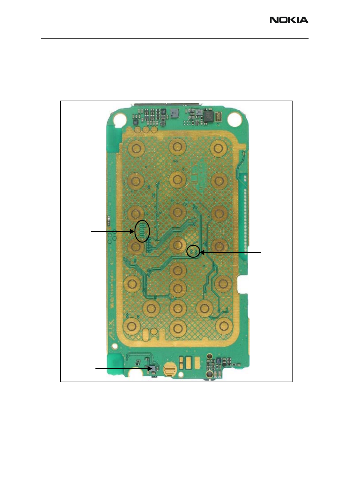
Mobile Terminal Components
The mobile terminal includes two PWB boards, the main PWB and the UI PWB.
Main PWB
Following are the components of the main PWB.
Tx I/Q signal
test points
Tx power
detector
Rx I/Q signal
test points
Figure 1: Main PWB component layout - top
Page 6 ©2005 Nokia Corporation Company Confidential Issue 2 05/2005
Page 7

6255/6255i/6256/6256i (RM-19)
Nokia Customer Care RF Description and Troubleshooting
Cell coupler
Diplexer
Antenna
connector
VCO
PCS PA
Cell PA
Cell Tx filter
PCS Tx filter
N7000:
Tx Upconverter
PCS coupler
Cell duplexer
PCS duplexer
Synthesizer IC
Headset jack
Rx RF Cell filter
N7160:
Rx front-end
Rx RF PCS filter
Rx IF AMPS filter
VCTCXO
Rx IF CDMA filter
N7100:
Rx downconverter
FM radio IC
D2800
processor
Flash
Tomahawk
connector
UEM
Bluetooth IC
Figure 2: Main PWB component layout - bottom
Issue 2 05/2005 ©2005 Nokia Corporation Company Confidential Page 7
Page 8
6255/6255i/6256/6256i (RM-19)
RF Description and Troubleshooting Nokia Customer Care
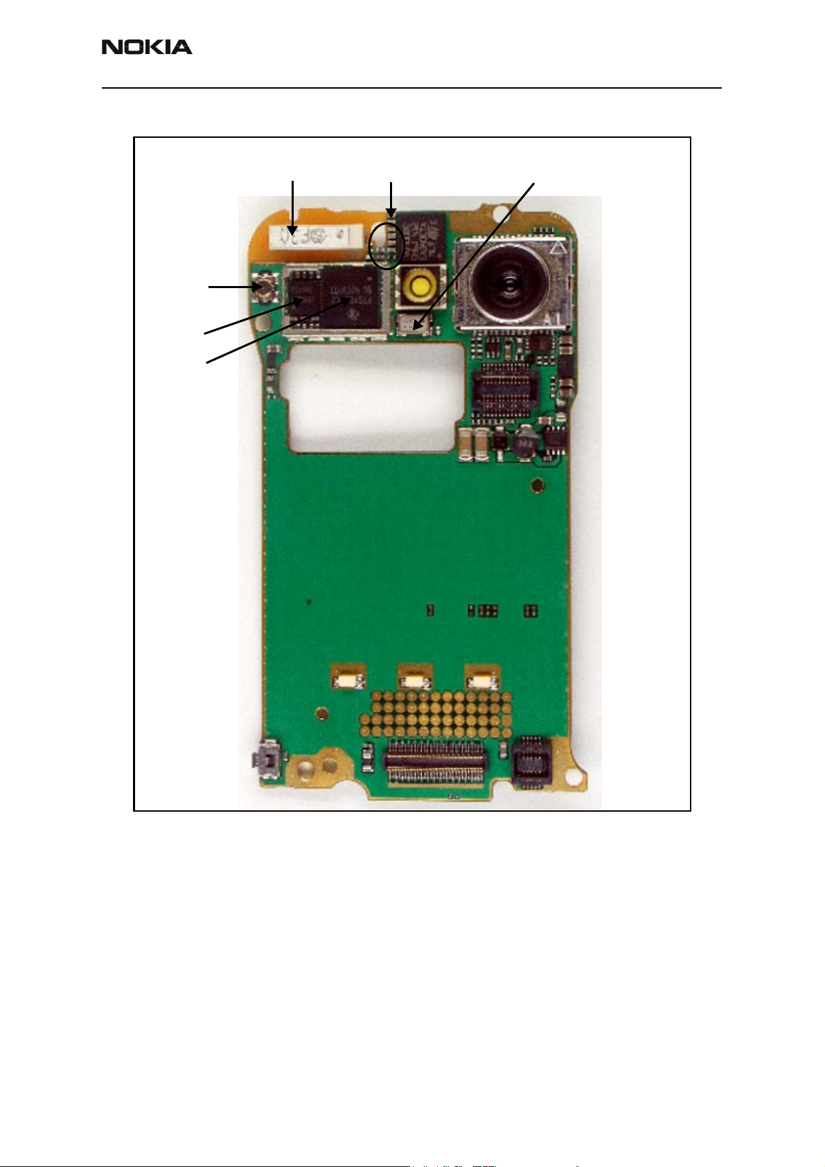
UI (Secondary) PWB
Following are the components of the UI PWB.
GPS ceramic filter
GPS LNA
GPS SAW filter
Figure 3: UI PWB component layout - top
Page 8 ©2005 Nokia Corporation Company Confidential Issue 2 05/2005
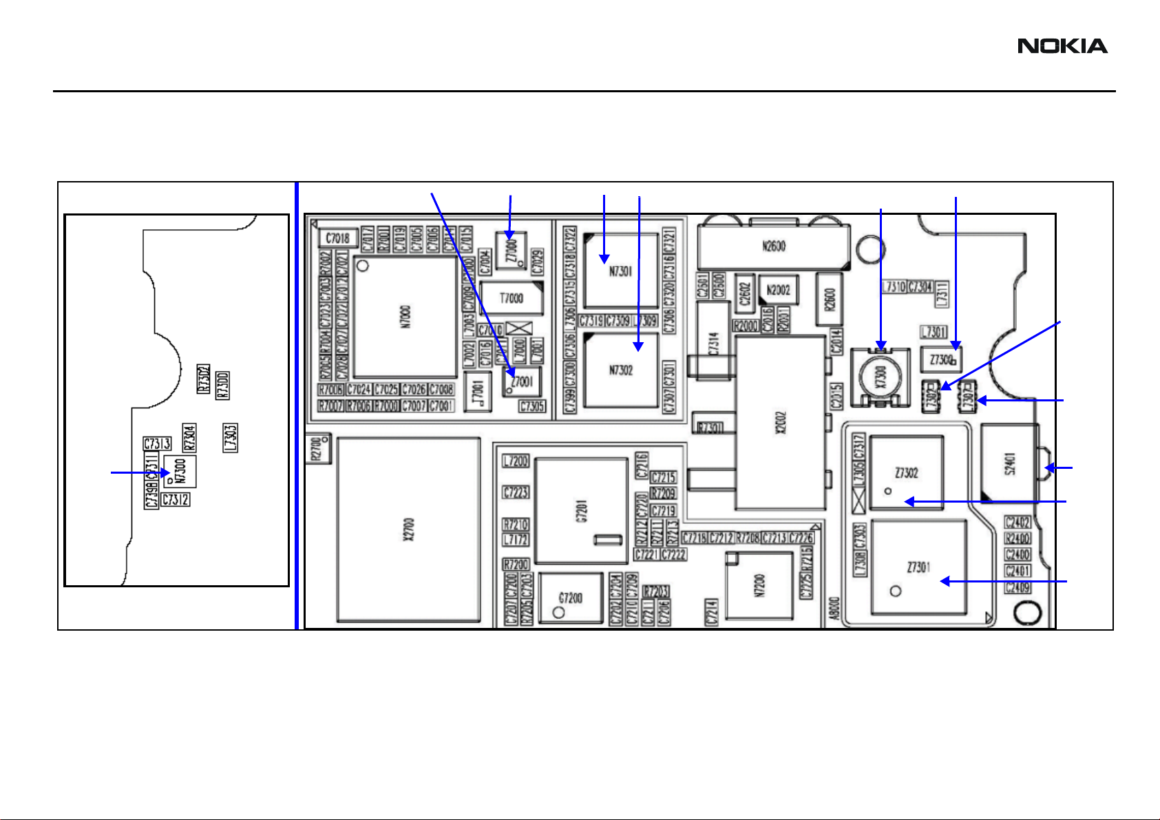
Page 9
6255/6255i/6256/6256i (RM-19)
Nokia Customer Care RF Description and Troubleshooting
GPS antenna
connector
GPS RF IC
GPS BB IC
GPS ceramic antenna
GPS antenna
matching circuitry
GPS 16.368 MHz
TCXO
Figure 4: UI PWB component layout - bottom
Issue 2 05/2005 ©2005 Nokia Corporation Company Confidential Page 9
Page 10

6255/6255i/6256/6256i (RM-19)
RF Description and Troubleshooting Nokia Customer Care
Preliminary RF Troubleshooting
The following sections identify steps to troubleshoot some common RF issues.
Mobile Terminal Cannot Make a Call
Verify the following if the mobile terminal cannot make a call:
1. The mobile terminal is in Normal Mode (i.e., the mobile terminal is searching for
a signal, net server is on).
2. The Preferred Roaming List (PRL) is loaded into the mobile terminal.
3. The mobile terminal is tuned and has passed tuning. Read the tuning parameters
using the Read Parameters component in Phoenix. An untuned mobile terminal
has all zeros in the tuning file.
4. The call box channel is set for a channel in PRL.
5. The SID is correct and entered into the mobile terminal.
6. The VCTCXO is centered as described in the "VCTCXO Manual Tuning" section on
7. The transmitter and receiver are working properly in Local Mode. See
Tx Power Low
Complete the following steps if Tx power is low:
1. Use Phoenix to turn on the transmitter in Local Mode.
2. Perform a visual inspection of the PWB under a microscope to check for the
3. Look for the presence of a Tx signal on a spectrum analyzer at the correct
page 54.
"Transmitter RF Troubleshooting" on page 11 and "Receiver RF
Troubleshooting" on page 31 for detailed information.
proper placement, rotation, and soldering of components.
frequency.
• If a signal is present but off-frequency, check the synthesizers for proper
frequency and amplitude. One of the synthesizers may be unlocked or the
VCO has no output signal.
• If a signal is not present or is present but is low in amplitude, check the
probing diagrams to determine where in the chain the fault occurs. (See "Tx
RF Test Points - Bottom Side" on page 28.)
4. Ensure that the power supplies to the Tx have the correct voltage. (See "Tx DC
Test Points - Bottom Side" on page 25)
5. Ensure that the AGC PDMs are set for the desired Tx power and that the AGC
voltages are correct. (See "AMPS Tx Setup" on page 15, "Cell Tx
Setup" on page 18, or "PCS Setup" on page 20.)
Page 10 ©2005 Nokia Corporation Company Confidential Issue 2 05/2005
Page 11
6255/6255i/6256/6256i (RM-19)
RF Description and Troubleshooting Nokia Customer Care
Transmitter RF Troubleshooting
Following are the main Tx RF components.
Antenna
connector
Diplexer
Cell
coupler
PCS
coupler
TOP SIDE
PCS Tx SAW filter
Cell PACell Tx SAW filter
PCS PA
BOTTOM SIDE
Power
detector
Power
switch
PCS
duplexer
Cell
duplexer
Figure 5: Main transmitter RF components
Page 11 ©2005 Nokia Corporation Company Confidential Issue 2 05/2005
Page 12
6255/6255i/6256/6256i (RM-19)
RF Description and Troubleshooting Nokia Customer Care
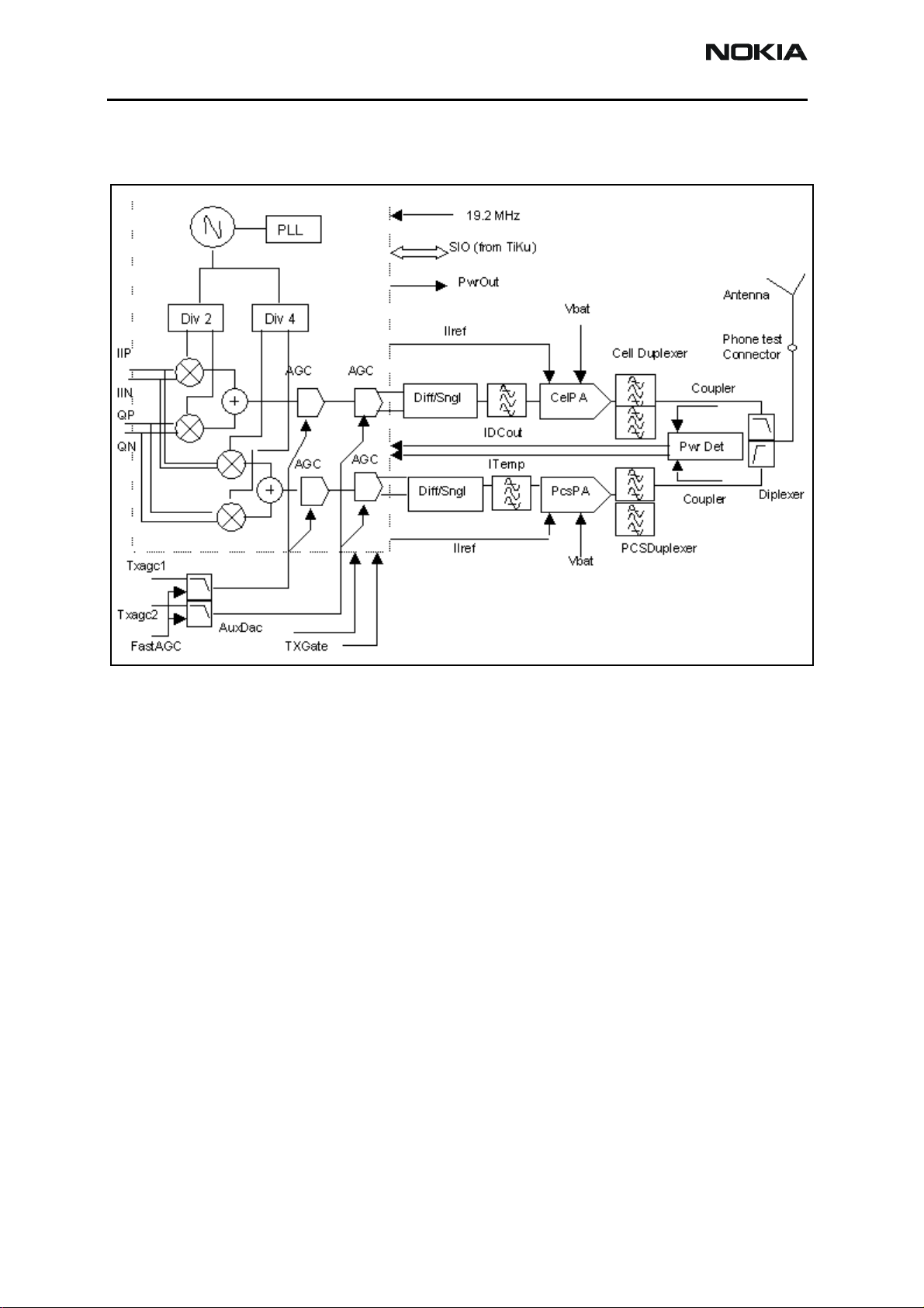
Transmitter Block Diagram
Following is the block diagram for the Tx RF system.
N7000 Tx IC
Figure 6: Tx system block diagram
Page 12 ©2005 Nokia Corporation Company Confidential Issue 2 05/2005
Page 13
6255/6255i/6256/6256i (RM-19)
RF Description and Troubleshooting Nokia Customer Care
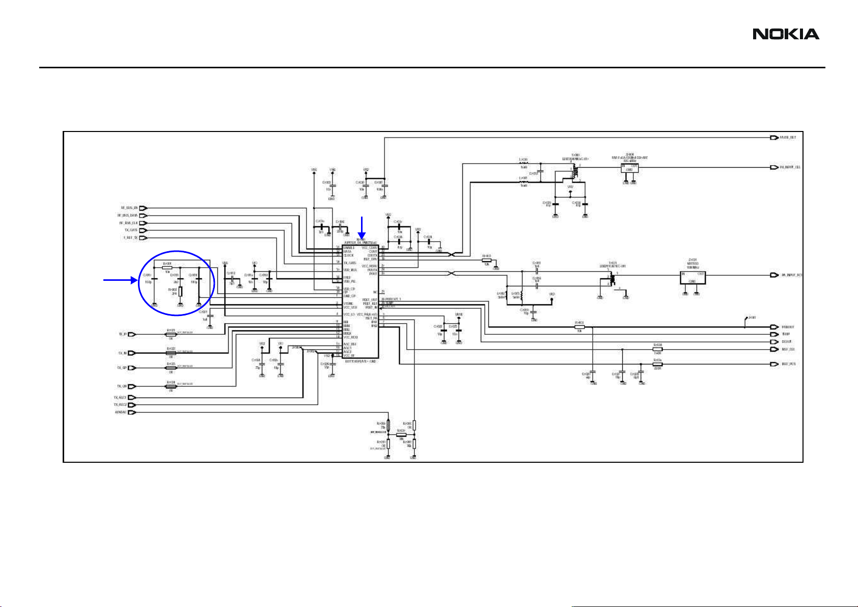
Transmitter Schematics
The following schematics are for general reference only. See the Schematics chapter for detailed versions.
Cell Tx filter
N7000 Tx IC
PCS Tx filter
Tx LO lock
voltage
Loop filter
Figure 7: Transmitter schematic 1
Page 13 ©2005 Nokia Corporation Company Confidential Issue 2 05/2005
Page 14
6255/6255i/6256/6256i (RM-19)
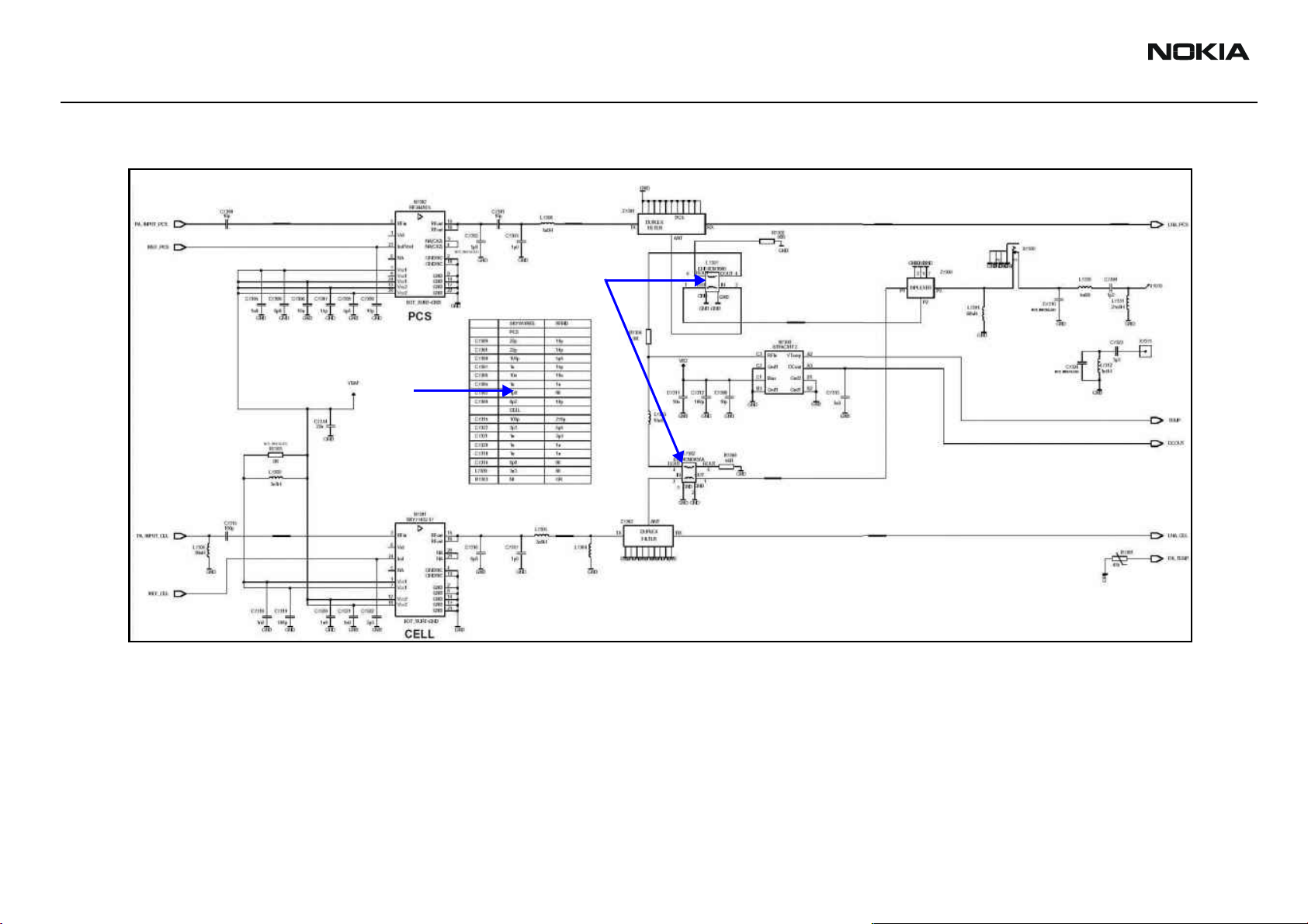
RF Description and Troubleshooting Nokia Customer Care
PCS PA
PCS PA
Component
changes based
on PA
manufacturer
Cell PA
PCS duplexer
Diplexer
Couplers
Power detector
Cell duplexer
Figure 8: Transmitter schematic 2
Page 14 ©2005 Nokia Corporation Company Confidential Issue 2 05/2005
Page 15

6255/6255i/6256/6256i (RM-19)
Nokia Customer Care RF Description and Troubleshooting
Transmitter Troubleshooting Setup
Use the following sets of procedures to troubleshoot the transmitter using Phoenix. Due
to the compact layout of the mobile terminal, some of the major test points are not
accessible without destroying the shield frames and the EL lamp. For example, duplexers/
diplexer/couplers test points are blocked by the test jig, the PA test points are
underneath the shield frame, and the BBIQ points are underneath the EL lamp.
To minimize effort, check the following in order:
1. Tx power at the RF connector.
2. All Tx DC points.
3. All soldering jig points for the whole Tx chain.
4. UHF LO presence:
• If the UHF LO is present, check the N7000 output.
• If the UHF LO is not present, it is a synthesizer problem.
5. If there is no N7000 output:
6. If there are several failed mobile terminals with the same symptoms, it may be
Use the following sections to set up troubleshooting in Phoenix according to the band
you are using:
• "AMPS Tx Setup" on page 15
• "Cell Tx Setup" on page 18
• "PCS Setup" on page 20
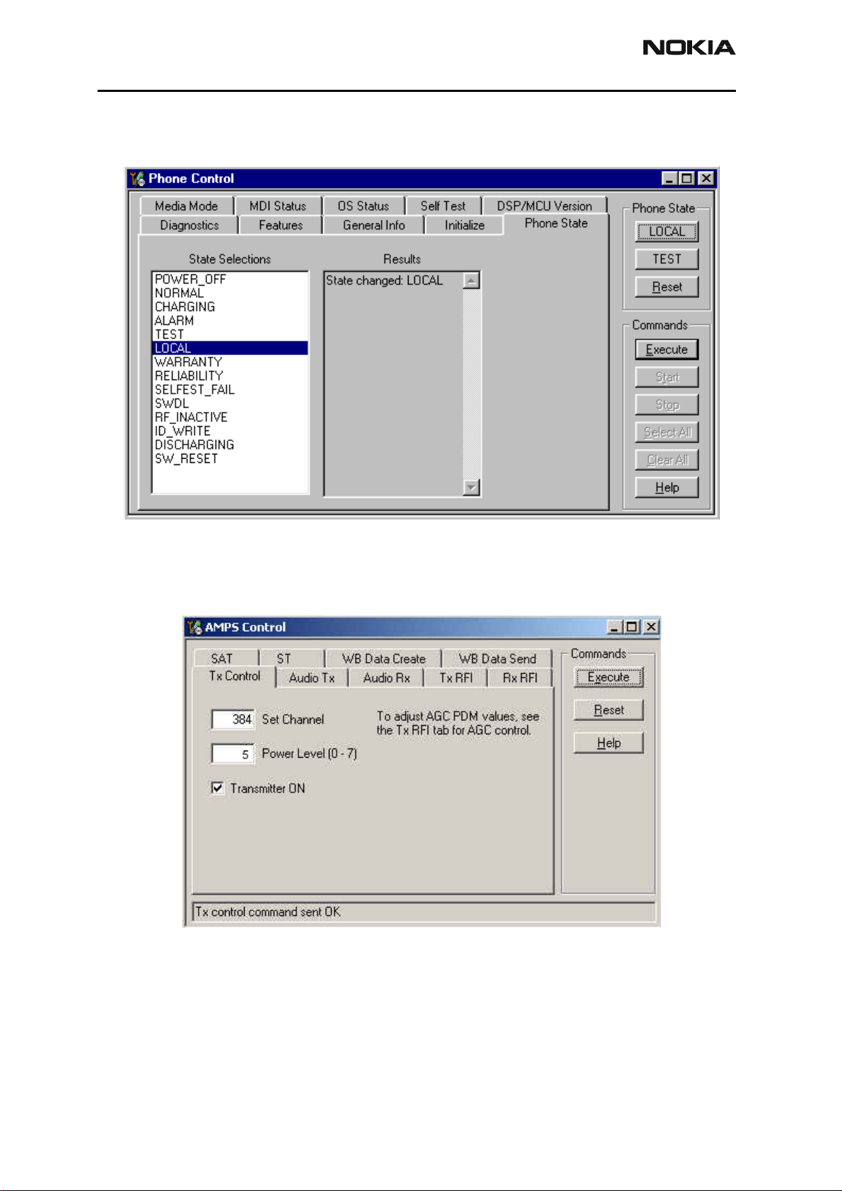
AMPS Tx Setup
Use the following procedures to prepare for AMPS Tx troubleshooting using Phoenix.
1. Connect the RF test connector to a spectrum analyzer.
2. Connect the mobile terminal to the PC via a test jig. (The bottom connector is a
a. Change the N7000.
b. If the problem persists, reflow the duplexers, diplexer, and couplers.
c. If the problem persists, change the PA.
necessary to break one to determine the cause.
USB port.)
3. Connect a power supply to the mobile terminal.
4. Open the Troubleshooting menu, and click Phone Control.
The Phone Control dialog box appears.
Issue 2 05/2005 ©2005 Nokia Corporation Company Confidential Page 15
Page 16
6255/6255i/6256/6256i (RM-19)
RF Description and Troubleshooting Nokia Customer Care
5. Click the LOCAL button in the Phone State area to put the mobile terminal into
Local Mode.
Figure 9: Phone Control dialog box
6. Open the Troubleshooting menu, point to AMPS, and click AMPS Control.
The AMPS Control dialog box appears.
Figure 10: AMPS Control dialog box
7. Click the Tx Control tab.
8. In the Set Channel field, type 384.
9. In the Power Level field, type 5.
10. Select the Transmitter ON option, and click Execute.
Page 16 ©2005 Nokia Corporation Company Confidential Issue 2 05/2005
Page 17
6255/6255i/6256/6256i (RM-19)
Nokia Customer Care RF Description and Troubleshooting
11. Configure the spectrum analyzer using the following values:
• Center Frequency = 836.52 MHz
• Span = 100 MHz
• Amplitude = 20 dBm
• Attenuation = Auto
• BW = Auto
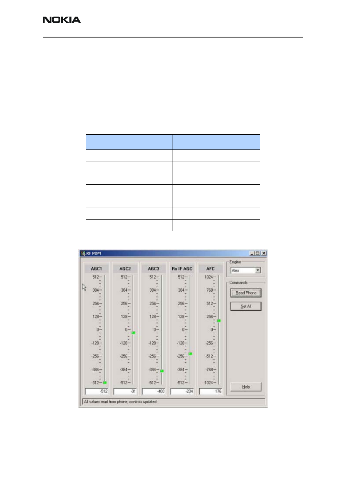
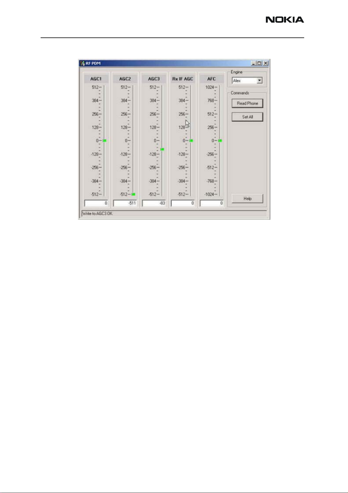
Table 1: RF PDM Values at Power Level 5
Description/Field Reference Value
AGC1 -512
AGC2 -31
AGC3 -400
Rx IF AGC -234
AFC +176
Pout at RF connector +14dBm
Current 400-500mA
Figure 11: RF PDM dialog box for AMPS
12. Click Read Phone to update the values.
Issue 2 05/2005 ©2005 Nokia Corporation Company Confidential Page 17
Page 18
6255/6255i/6256/6256i (RM-19)
RF Description and Troubleshooting Nokia Customer Care
Cell Tx Setup
Use the following procedures to prepare for Cell Tx troubleshooting using Phoenix.
1. Connect an RF test connector to a call box.
2. Connect the mobile terminal to the PC via a test jig. (The bottom connector is a
USB port.)
3. Connect a power supply to the mobile terminal.
4. On the Phone Control dialog box, click the LOCAL button in the Phone State
area to put the mobile terminal into Local Mode. (See Figure 9 on page 16.)
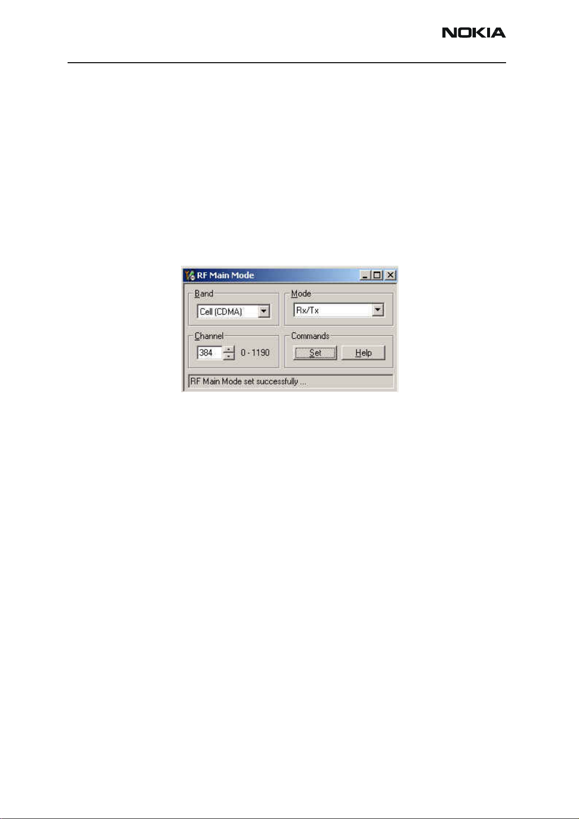
5. Open the Troubleshooting menu, point to RF, and click RF Main Mode.
The RF Main Mode dialog box appears.
Figure 12: RF Main Mode dialog box for Cell Mode
6. Select the following values on the RF Main Mode dialog box:
• Band = Cell (CDMA)
• Channel = 384
• Mode = Rx/Tx
7. Click Set.
Note: Be sure that the “RF Main Mode set successfully” message appears in the status bar.
8. Open the Troubleshooting menu, point to RF, and click CDMA Control.
Page 18 ©2005 Nokia Corporation Company Confidential Issue 2 05/2005
Page 19
6255/6255i/6256/6256i (RM-19)
Nokia Customer Care RF Description and Troubleshooting
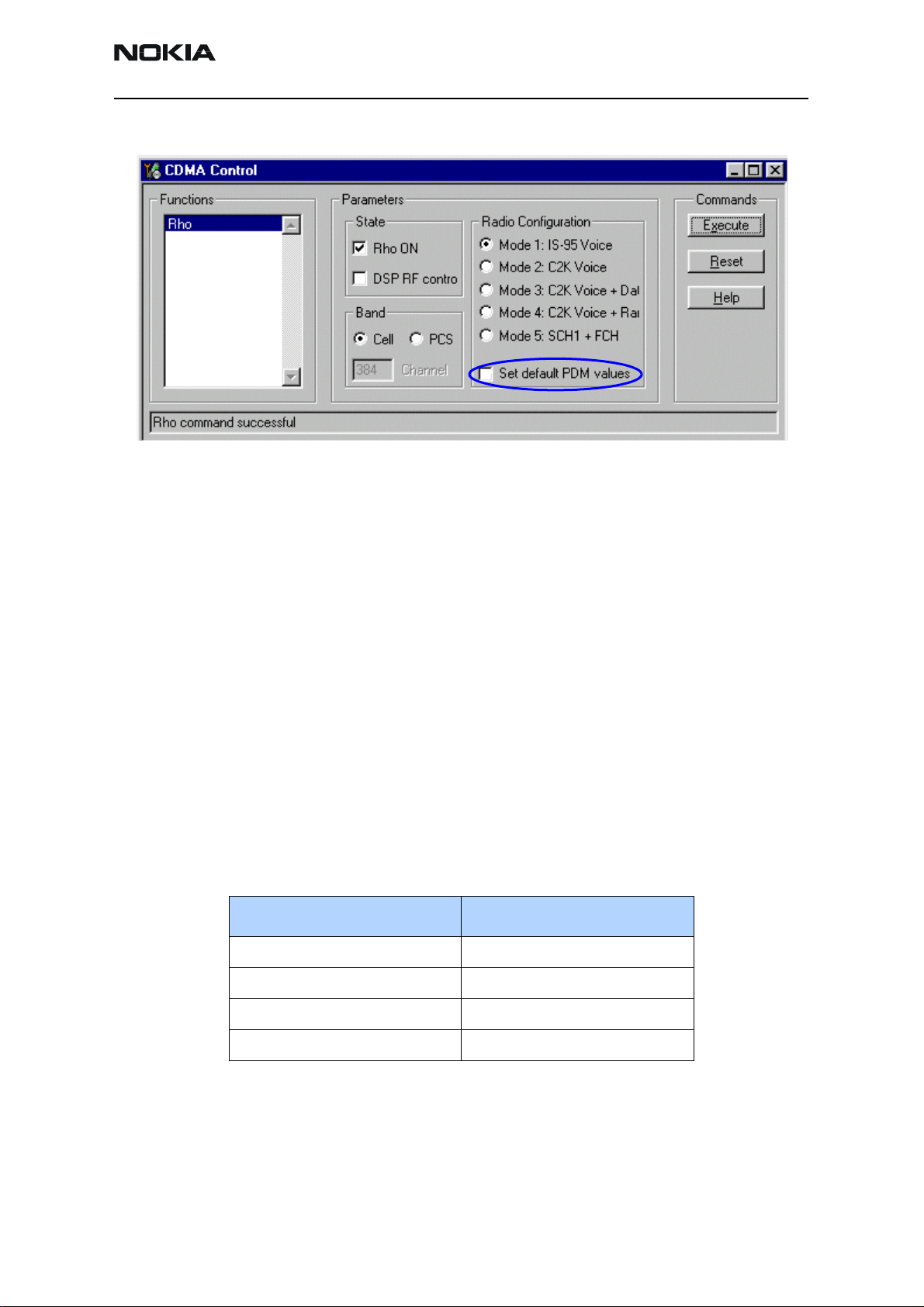
The CDMA Control dialog box appears.
Do NOT select
this option
Figure 13: CDMA Control dialog box for Cell Tx troubleshooting
9. Select the following values:
• State = Rho ON
• Band = Cell
• Radio Configuration = Mode 1: IS-95 Voice
Note: Do NOT select the Set default PDM values option
10. Click Execute.
11. Configure the spectrum analyzer using the following values:
• Center Frequency = 836.52 MHz
• Span = 100 MHz
• Amplitude = 20 dBm
• Attenuation = Auto
• BW = Auto
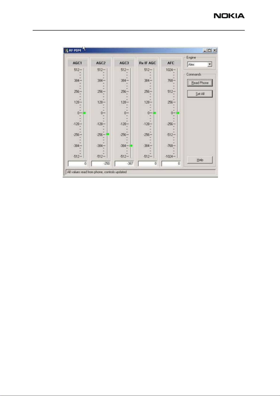
Table 2: RF PDM Values
Description/Field Reference Value
AGC2 -250
AGC3 -387
Pout at RF connector +20dBm
Current 500-600mA
Issue 2 05/2005 ©2005 Nokia Corporation Company Confidential Page 19
Page 20
6255/6255i/6256/6256i (RM-19)
RF Description and Troubleshooting Nokia Customer Care
PCS Setup
Use the following procedures to prepare for PCS Tx troubleshooting using Phoenix.
Figure 14: RF PDM Control dialog box for Cell band
12. Click Read Phone to update the values.
1. Connect an RF test connector to a call box.
2. Connect the mobile terminal to the PC via a test jig. (The bottom connector is a
USB port.)
3. Connect a power supply to the mobile terminal.
4. Open the Troubleshooting menu, and point to Phone Control.
The Phone Control dialog box appears. (See Figure 9 on page 16.)
5. Click the LOCAL button in the Phone State area to put the mobile terminal into
Local Mode.
6. Open the Troubleshooting menu, point to RF, and click RF Main Mode.
The RF Main Mode dialog box appears. (See Figure 12 on page 18.)
Page 20 ©2005 Nokia Corporation Company Confidential Issue 2 05/2005
Page 21
6255/6255i/6256/6256i (RM-19)
Nokia Customer Care RF Description and Troubleshooting
7. Select the following values on the RF Main Mode dialog box:
• Band = PCS (CDMA)
• Channel = 600
• Mode = Rx/Tx
8. Click Set.
Note: Be sure that the “RF Main Mode set successfully” message appears in the status bar.
9. Open the Troubleshooting menu, point to RF, and click CDMA Control.
The CDMA Control dialog box appears. (See Figure 13 on page 19.)
10. Select the following values on the CDMA Control dialog box.
• State = Rho ON
• Band = PCS
• Radio Configuration = Mode 1: IS-95 Voice
Note: Do NOT select the Set default PDM values option.
11. Click Execute.
12. Open the Troubleshooting menu, point to RF, and click PDM Control.
13. Configure the spectrum analyzer using the following values:
• Center Frequency = 1880 MHz
• Span = 100 MHz
• Amplitude = 20 dBm
• Attenuation = Auto
• BW = Auto
Table 3: RF PDM Values
Description/Field Reference Value
AGC2 -511
AGC3 -83
Pout at RF connector +23dBm
Current 700-800mA
Issue 2 05/2005 ©2005 Nokia Corporation Company Confidential Page 21
Page 22
6255/6255i/6256/6256i (RM-19)
RF Description and Troubleshooting Nokia Customer Care
Figure 15: RF PDM Control dialog box for PCS band
14. Click Read Phone to update the values.
Transmitter RF Troubleshooting Procedures
After Phoenix is set up using either the AMPS, Cell, or PCS setup procedures, use the
following steps to troubleshoot the transmitter.
1. Using a voltmeter, check to see that all VR2, VR6, and VR1B are on the transmit
system. (See "Tx DC Test Points - Bottom Side" on page 25.)
• If any are missing, look for SMD problems around the N7000 and the UEME.
• If SMD is good, replace the UEME.
2. Once all DC voltages are present, check the AGC control voltages. (See "AMPS Tx
Setup" on page 15, "Cell Tx Setup" on page 18, or "PCS Setup" on page 20.)
• If the voltages are incorrect, check the SMD around TX_AGC1 and TX_AGC2.
• If the SMDs are correct, replace the D2800.
3. Using an oscilloscope, check the input modulation BBIQ wave forms at R7021,
R7022, R7023, and R7024. They should all be present with an AC swing of about
500mVpp, with an offset of +1.2V.
• If one or more waveforms are missing, look for SMD problems around these
resistors.
• If the SMD is good, replace the UEM.
Page 22 ©2005 Nokia Corporation Company Confidential Issue 2 05/2005
Page 23

6255/6255i/6256/6256i (RM-19)
Nokia Customer Care RF Description and Troubleshooting
4. Use an AAS-10 RF probe to probe the Cell Tx output of the N7000.
• If there is no RF or low RF, look for SMD everywhere around the N7000.
• If the SMD is okay, replace the N7000.
5. Probe the PA input.
• If the level is low, look for an SMD issue on the Tx filter or matching
transformer (T7001 or T7002).
• Reflow or replace the filter as necessary.
6. Probe the PA output.
• If the RF is missing or low, look for Vbatt voltages and SMD issues on and
around the PA.
• If these are okay, replace the PA.
7. Probe the duplexer output.
• If the RF is missing or low, reflow or replace the duplexer.
8. Probe the coupler output.
• If the RF is missing or low, reflow or replace the coupler.
9. Probe the diplexer output.
• If the RF is missing or low, reflow or replace the diplexer.
Failed Test: Tx PA Detector
Use the following steps if you encounter a failed test for the Tx PA detector:
1. Use Phoenix to set the mobile terminal into Local Mode and activate the Tx with
default output power.
2. The output power at the RF test connector should be 15dBm +/- 4dB. If not,
follow the procedures in the "Transmitter RF Troubleshooting Procedures" section
on page 22.
3. Using a voltmeter on DC, probe the detector output at C7313. The voltmeter
should read approximately 1.4V. If not, replace N7300. (See page 26 for test
point locations and common power and voltage variations.)
Issue 2 05/2005 ©2005 Nokia Corporation Company Confidential Page 23
Page 24
6255/6255i/6256/6256i (RM-19)
RF Description and Troubleshooting Nokia Customer Care
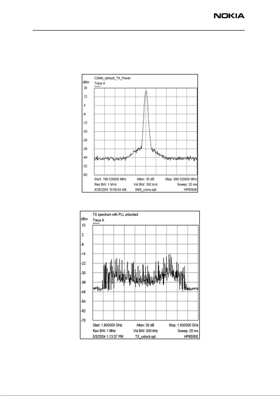
Tx Output Spectrum
Following is the correct output of the mobile terminal on a spectrum analyzer with
100MHz span. Note that if you are using the AAS-10 probe with the mobile terminal
connected to the call box, the amplitude should be approximately -7dBm at the antenna
test point on the top of the PWB.
Figure 16: Correct output spectrum
Following is an example of incorrect output.
Figure 17: Incorrect output spectrum
Page 24 ©2005 Nokia Corporation Company Confidential Issue 2 05/2005
Page 25

6255/6255i/6256/6256i (RM-19)
Nokia Customer Care RF Description and Troubleshooting
Tx DC Test Points - Bottom Side
Following are the Tx DC test points located on the bottom side of the main PWB.
1
6
7
2 3
4
5
8
9
10
Figure 18: Tx DC test points on the bottom side of the main PWB
Issue 2 05/2005 ©2005 Nokia Corporation Company Confidential Page 25
Page 26

6255/6255i/6256/6256i (RM-19)
RF Description and Troubleshooting Nokia Customer Care
Table 4 shows the values for the test points in Figure 18.
Table 4: Tx DC Test Point Description and Values - Main PWB - Bottom Side
Test
Point
1 Tx UHF LO Lock voltage: ~1.2V
2VR6 2.8V
3 Vbatt Cell*
4 Vbatt PCS*
5VR1B 4.8V
6AGC1 0.1V to 1.8V
7AGC2 0.1V to 1.8V
8VR6 2.8V
9VR2 2.8V
10 VR1B 4.8V
Description Values
*Vbatt also appears at the outputs of the PAs.
Tx DC and RF Test Points - Top Side
Following are the Tx DC and RF test points located on the top side of the main PWB.
5
4
1
2
3
Figure 19: Tx DC and RF test points on the top side of the main PWB
6
Page 26 ©2005 Nokia Corporation Company Confidential Issue 2 05/2005
Page 27

6255/6255i/6256/6256i (RM-19)
Nokia Customer Care RF Description and Troubleshooting
Table 5 shows the values for the test points in Figure 19.
Table 5: Tx DC Test Point Description and Values - Main PWB - Top Side
Test
Point
1 Power detector input AMPS: -5dBm at 836.25MHz
2 Power detector output AMPS/Cell:
3 Power detector VR2 2.8V
4AGC2 0.1V to 1.8V
5AGC1 0.1V to 1.8V
6 Tx IQ in ~1.2V
Description Values
Cell: -3dBm at 836.25MHz
PCS: -6dBm at 1880MHz
1.9V at <5dBm
1.8V at 15dBm
1.2V at 25dBm
PCS:
1.9V at <5dBm
1.8V at 15dBm
1.3V at 25dBm
With oscilloscope:
Approximately 500 mV p-p with
+1.2V offset
Issue 2 05/2005 ©2005 Nokia Corporation Company Confidential Page 27
Page 28

6255/6255i/6256/6256i (RM-19)
RF Description and Troubleshooting Nokia Customer Care
Tx RF Test Points - Bottom Side
Figure 20 shows the Tx RF test points located on the bottom side of the main PWB.
4
1
2
53
Figure 20: Tx DC and RF test points on the bottom side of the main PWB
Table 6 shows the values for the test points in Figure 20. These values are based on a PCS
frequency of 1880MHz and an AMPS/Cell frequency of 836.25MHz.
Table 6: Tx RF Test Point Descriptions and Values - Main PWB - Bottom Side
Test
Point
1 Tx UHF LO Cell: 3346.08MHz -57dBm
2 PCS N7000 out -15dBm
3 Cell N7000 out Cell: -8dBm
Description Values
PCS: 3760MHz -54dBm
AMPS: -15dBm
Page 28 ©2005 Nokia Corporation Company Confidential Issue 2 05/2005
Page 29

6255/6255i/6256/6256i (RM-19)
Nokia Customer Care RF Description and Troubleshooting
Table 6: Tx RF Test Point Descriptions and Values - Main PWB - Bottom Side (Continued)
Test
Point
4 PCS PA out 11dBm
5 RF out AMPS: +14dBm
Description Values
RF Power Supply DC Test Points - Bottom Side
Following are the RF power supply DC test points located on the bottom side of the main
PWB.
Cell: +20dBm
PCS: +20dBm
1
2
3
4
5
Figure 21: RF power supply DC test points on the bottom side of the main PWB
6
7
8
9
10
Issue 2 05/2005 ©2005 Nokia Corporation Company Confidential Page 29
Page 30

6255/6255i/6256/6256i (RM-19)
RF Description and Troubleshooting Nokia Customer Care
Table 7 shows the values for the test points in Figure 21.
Table 7: RF Power Supply DC Test Points (Main PWB - Bottom Side)
Probe
Point
1 VIO 1.8V
2 VrefRF1 1.4V (Tx)
3 VR7 2.8V (Rx)
4 VR6 2.8V (Tx)
5 VR2 2.8V (Tx)
6 VR3 2.8V (Synthesizer)
7 VR5 2.8V (Rx)
8 VR4 2.8V (Rx)
9 VR1A 4.7V (Synthesizer)
10 VR1B 4.7V (Tx)
Description Value
Page 30 ©2005 Nokia Corporation Company Confidential Issue 2 05/2005
Page 31

6255/6255i/6256/6256i (RM-19)
Nokia Customer Care RF Description and Troubleshooting
Receiver RF Troubleshooting
The heart of the receiver is the N7160 Rx IC, which contains two LNAs and mixers. The
other components are passive. There are two RF SAW filters for the Cell and PCS bands.
In addition, there are two additional IF filters, an IF SAW for CDMA and an IF Crystal for
AMPS. The back-end of the receiver consists of the N7100 IC, which handles the VGA and
IQ demodulator functions.
Issue 2 05/2005 ©2005 Nokia Corporation Company Confidential Page 31
Page 32

6255/6255i/6256/6256i (RM-19)
Nokia Customer Care RF Description and Troubleshooting
Receiver Block Diagram
Following is the Rx system block diagram.
Figure 22: Receiver system block diagram
Issue 2 05/2005 ©2005 Nokia Corporation Company Confidential Page 32
Page 33

6255/6255i/6256/6256i (RM-19)
Nokia Customer Care RF Description and Troubleshooting
Receiver Schematics
The following schematics are for general reference only. See the Schematics chapter for detailed versions.
Cell RF SAW filter
N7160 Rx
front-end IC
PCS RF SAW filter
AMPS IF crystal filter
CDMA IF SAW filter
Figure 23: Receiver schematics - 1
Issue 2 05/2005 ©2005 Nokia Corporation Company Confidential Page 33
Page 34

6255/6255i/6256/6256i (RM-19)
RF Description and Troubleshooting Nokia Customer Care
Loop filter
Rx LO lock voltage
1.2 to 1.7 Vdc
N7100 Rx downconverter
Figure 24: Receiver schematic - 2
Page 34 ©2005 Nokia Corporation Company Confidential Issue 2 05/2005
Page 35

6255/6255i/6256/6256i (RM-19)
Nokia Customer Care RF Description and Troubleshooting
RF AGC Status
When configuring the values on the RF AGC Status dialog box, note the following:
• The RF AGC status functionality only works in Call Mode.
•In the PLL Lock Status area, bright green indicates a locked PLL and dark green
indicates an unlocked PLL.
•In the Baseband Type field, ensure that the correct baseband is selected
(Tiku BB 4.5).
• Clicking the Stop Updating button allows you to toggle between the Update
Every 2 Seconds and Stop Updating functions.
AFC PDM settings
LNA Gain (High[Boost for PCS]/Low)
Rx IF AGC PDM settings
BBAMP Gain Settings
PA AGC PDM settings
Figure 25: RF AGC Status dialog box
Tx AGC 2 PDM settings
Tx AGC 1 PDM settings
Issue 2 05/2005 ©2005 Nokia Corporation Company Confidential Page 35
Page 36

6255/6255i/6256/6256i (RM-19)
RF Description and Troubleshooting Nokia Customer Care
Turning on the Rx Path
Use the following steps to turn on the Rx path using Phoenix.
1. On the Phone Control dialog box, click the LOCAL button in the Phone State
area to put the mobile terminal into Local Mode.
Figure 26: Phone Control dialog box
2. Click the Execute button.
3. Depending on the band, use the applicable settings from the table below on the
RF Main Mode dialog box.
Table 8: RF Main Mode Dialog Box Settings
Band Mode Channel
AMPS Rx = 881.52 MHz 384
Cell Rx = 881.52 MHz 384
PCS Rx = 1960 MHz 600
Page 36 ©2005 Nokia Corporation Company Confidential Issue 2 05/2005
Page 37

6255/6255i/6256/6256i (RM-19)
Nokia Customer Care RF Description and Troubleshooting
Figure 27: RF Main Mode dialog box for AMPS (top), Cell (middle), and PCS (bottom)
Issue 2 05/2005 ©2005 Nokia Corporation Company Confidential Page 37
Page 38

6255/6255i/6256/6256i (RM-19)
RF Description and Troubleshooting Nokia Customer Care
Switching the Rx Gain States
Use the RF Gen I/O dialog box to switch the gain state (Hi and Lo) for CDMA and AMPS
modes.
High Gain State (default)
Cell
AMPS
Low Gain State
PCS
Checking AMPS from RF to IQ
Use the following steps to check the AMPS receiver functionality from RF to IQ output.
1. Start Phoenix in Local Mode with only the Rx path turned on.
2. Inject a –75dBm CW signal of 881.53MHz (i.e. 10kHz offset from 881.52MHz)
into the RF.
3. Measure a 10kHz tone on the analyzer. You should see a typical -20Bm IQ tone
for AMPS.
CDMA
Figure 28: RF Gen I/O dialog box
Page 38 ©2005 Nokia Corporation Company Confidential Issue 2 05/2005
Page 39

6255/6255i/6256/6256i (RM-19)
Nokia Customer Care RF Description and Troubleshooting
Figure 29: Receiver IQ Level on AMPS band
Figure 30 shows the AMPS spectrum and the test points located on the top side of the
main PWB. All four test points should be approximately equal. WARNING: Direct current
is present on these test points.
Figure 30: AMPS spectrum and the test points on the top side of the main PWB
Checking Cell Receiver from RF to IQ
Use the following values to check the Cell receiver functionality RF to IQ output.
Rx_IP
Rx_IN
Rx_QP
Rx_QN
1. Start Phoenix in Local Mode with only the Rx path turned on.
2. Inject a –75dBm CW signal of 881.82MHz (i.e. 300kHz offset from 881.52MHz or
10 channels away).
Issue 2 05/2005 ©2005 Nokia Corporation Company Confidential Page 39
Page 40

6255/6255i/6256/6256i (RM-19)
m
RF Description and Troubleshooting Nokia Customer Care
3. Measure a 300kHz tone on the analyzer. You should see a typical -21dBm IQ tone
for CDMA Cell.
Cell I Q Output
dBm
0
-10
-20
-30
-40
-50
-60
-70
Trace A
1
Trace A
302 kHz
1
-21.2500 dB
-80
-90
-100
Centre: 300 kHz Span: 200 kHzAtten: 10 dB
Res BW: 3 kHz Vid BW: 3 kHz Sweep: 100 ms
5/5/2004 3:29:30 PM HP8595ECellIQ.spt
Figure 31: Receiver IQ level on Cell band
Figure 32 shows the Cell spectrum and the test points located on the top side of the
main PWB. All four test points should be approximately equal. WARNING: Direct current
is present on these test points.
Rx_IP
Rx_IN
Rx_QP
Rx_QN
Figure 32: Cell spectrum and test points on the top side of the main PWB
Page 40 ©2005 Nokia Corporation Company Confidential Issue 2 05/2005
Page 41

6255/6255i/6256/6256i (RM-19)
Nokia Customer Care RF Description and Troubleshooting
Checking PCS Receiver from RF to IQ
Use the following values to check the PCS receiver functionality from RF to IQ output.
1. Start Phoenix in Local Mode with only the Rx path turned on.
2. Inject a –75dBm CW signal of 1960.5MHz (i.e. 500kHz offset from 1960MHz or
10 channels away).
3. Measure a 500kHz tone on the analyzer. (If a 300kHz tone works but a 500kHz
tone does not, the problem is in the BB filter, possibly not set by Phoenix.) You
should see a typical -22dBm IQ tone for CDMA PCS.
Figure 33: Receiver IQ Level on PCS Band
Figure 33 shows the PCS spectrum and the test points located on the top side of the
main PWB. All four test points should be approximately equal. WARNING: Direct current
is present on these test points.
Issue 2 05/2005 ©2005 Nokia Corporation Company Confidential Page 41
Page 42

6255/6255i/6256/6256i (RM-19)
RF Description and Troubleshooting Nokia Customer Care
Figure 34: PCS spectrum and the test points on the top side of the main PWB
Receiver Diagnostic Signal Tracing
Use the following steps to trace the receiver signal.
1. Inject an external signal source of –25dBm to the RF input. An Agilent call box
8960 is recommended.
2. Press the Call Setup button, press the Active Cell soft button, and select CW.
3. Inject a CW signal for PCS (1960MHz) or Cell/AMPS (881.52MHz) at a fixed
-25dBm power level.
Rx_IP
Rx_IN
Rx_QP
Rx_QN
4. Use an AAS-10 probe to take measurements. Signal levels are approximate, and
accuracy may be +/- 2dB or more depending on the position and grounding of
the probe.
Page 42 ©2005 Nokia Corporation Company Confidential Issue 2 05/2005
Page 43

6255/6255i/6256/6256i (RM-19)
Nokia Customer Care RF Description and Troubleshooting
Receiver DC Test Points
1
4
6
2
Figure 35: Receiver DC troubleshooting test points on the bottom side of the main PWB
7
3
5
Table 9 includes the descriptions and values for the Rx DC test points from Figure 35.
Table 9: Receiver DC Test Point Values
Test
Point
1 Rx LO lock voltage 1.2 to 1.7 Vdc
2 LO Vdd 2.6 VDC LO Amp supply lines
3 RFA Vdd 2.8 VDC RF Amp Vdd supply
Description Value
for Cell and PCS
line for Cell band
4 C_LNA Vdd 2.8 VDC external VDd supply
line for Cell LNA
5 P_LNA Vdd 2.8 VDC external Vdd supply
line for PCS LNA
6 IFA Vdd 2.8 VDC IF Amp Vdd supply line
for CDMA and AMPS IFs
7 IFA Vdd 2.8 VDC IF Amp Vdd supply line
for CDMA and AMPS IFs
Issue 2 05/2005 ©2005 Nokia Corporation Company Confidential Page 43
Page 44

6255/6255i/6256/6256i (RM-19)
RF Description and Troubleshooting Nokia Customer Care
Receiver RF Test Points
1
7
6
3
5
Figure 36: Rx RF test points on the bottom side of the main PWB
Table 10 includes the descriptions and values for the Rx RF test points from Figure 36.
Table 10: Receiver RF Test Point Values
Test
Point
Description Value
2
4
1 PCS_CEL_LO (from VCO) Cell: 1009.62MHz at -15dBm
PCS: 2088.1MHz at -17dBm
2 Cell channel 384 (from duplexer) 881.52MHz at -33dBm
3 Cell channel 384 (to RF SAW) High gain: 881.52MHz at -21dBm
Low gain: 881.52MHz at -36dBm
4 PCS channel 600 (from duplexer) 1960MHz at -46dBm
Page 44 ©2005 Nokia Corporation Company Confidential Issue 2 05/2005
Page 45

6255/6255i/6256/6256i (RM-19)
Nokia Customer Care RF Description and Troubleshooting
Table 10: Receiver RF Test Point Values (Continued)
Test
Point
5 PCS channel 600 (to RF SAW) High gain: 1960MHz at -32dBm
6 IF MIX OUT (from N7160) High gain: 128.1MHz at -21dBm
7 IFA_IN (to N7160) High gain: 128.1MHz at -18dBm
Receiver IF Test Points
1
Description Value
Low gain: 1960MHz at -49dBm
Low gain: 128.1MHz at -34dBm
Low gain: 128.1MHz at -34dBm
6
5
7
4
3
Figure 37: Receiver IF test points on the bottom side of the main PWB
2
Table 11 includes the descriptions and values for Rx IF test points from Figure 37.
Table 11: Receiver IF Test Point Values
Test
Point
1 Rx VHF LO 256.2MHz at -70dBm
2 CDMA IF (to SAW) 128.1MHz High gain: Cell channel 384 at -9dBm
Description Value
Low gain: Cell channel 384 at -25dBm
High gain: PCS channel 600 at -8dBm
Low gain: PCS channel 600 at -24dBm
Issue 2 05/2005 ©2005 Nokia Corporation Company Confidential Page 45
Page 46

6255/6255i/6256/6256i (RM-19)
RF Description and Troubleshooting Nokia Customer Care
Table 11: Receiver IF Test Point Values (Continued)
Test
Point
3 CDMA_IF_P (to the N7100)
4 CDMA_IF_N Cell high gain: -29dBm
5 AMPS IF (to MCF) 128.1MHz High gain: Cell channel 384 at -19dBm
6 AMPS_IF_N (to the N7100)
7 AMPS_IF_P Cell high gain: -28dBm
Description Value
128.1MHz
128.1MHz
Receiver Logic Input Voltages
Figure 38 shows the receiver logic input voltages.
Cell high gain: -29dBm
Cell low gain: -45dBm
PCS high gain: -29dBm
PCS low gain: -45dBm
Cell low gain: -45dBm
PCS high gain: -29dBm
PCS low gain: -45dBm
Low gain: Cell channel 384 at -35dBm
Cell high gain: -28dBm
Cell low gain: -44dBm
Cell low gain: -44dBm
31
2
Figure 38: Receiver logic input voltage test points
Page 46 ©2005 Nokia Corporation Company Confidential Issue 2 05/2005
Page 47

6255/6255i/6256/6256i (RM-19)
Nokia Customer Care RF Description and Troubleshooting
Table 12 includes the measure logic levels for the N7160.
Table 12: Rx Front-end (N7160) Logic Levels
Logic Input Voltages
Mode
IF_SEL BAND GAIN_CTL
AMPS High Gain 2.8 V 0.1 V 2.8 V
AMPS Low Gain 2.8 V 0.1 V 0 V
Cell CDMA High Gain 0 V 0.1 V 2.8 V
Cell CDMA Low Gain 0 V 0.1 V 0 V
PCS CDMA High Gain 0 V 2.7 V 2.8 V
PCS CDMA Low Gain 0 V 2.7 V 0 V
If the logic levels are significantly off (+/- 0.2V), replace the N7160 and re-measure. If
the voltages are still out of specifications, refer to the Baseband Troubleshooting chapter.
N7160 Receiver Overview
Keep the following points in mind regarding the N7160 receiver:
• There is a separate LNA for 800MHz (Cell and AMPS) and 1900MHz (PCS).
• There is a separate RFA (inside N7160) for 800MHz (Cell and AMPS) and
1900MHz (PCS).
• After the RFA, there is a mixer, and then the signals are separated by CDMA (Cell
and PCS) and AMPS.
For example, if there is no IF frequency (128.1MHz) check both Cell and PCS. If
only one has 128.1MHz at L753, ensure that IF_SEL is working. If it is, then
replace the N750 due to a bad RFA.
If Cell and AMPS are working but PCS is not, look at the band select line and the
PCS LNA before replacing the N7160.
Issue 2 05/2005 ©2005 Nokia Corporation Company Confidential Page 47
Page 48

6255/6255i/6256/6256i (RM-19)
RF Description and Troubleshooting Nokia Customer Care
Cell
LNA
PCS
LNA
IFAs
LO
Buffer
Cell
RFA
PCS
RFA
Figure 39: N7160 receiver
There are two common explanations for an N7160 failure consisting of high current in
Local Mode with just the Rx turned on:
• No presence of an LO signal
• Input impedance drop is shorting out one of the DC supply pins to the chip
IMPORTANT: You must check for both conditions before replacing the chip. If you
have no LO signal, refer to "UHF Synthesizer" on page 56. If you have a significant supply
voltage drop on one of the supply pins, then replace the N7160.
Table 13: N7160 Conditions and Supply Currents
Condition: Local Mode, Set
Rx Only in RF Main Mode
Good mobile terminal 100mA
No UHF LO signal present 254mA
Pin 13 shorted 255mA
Supply Current
(From Power Supply)
Page 48 ©2005 Nokia Corporation Company Confidential Issue 2 05/2005
Page 49

6255/6255i/6256/6256i (RM-19)
Nokia Customer Care RF Description and Troubleshooting
Synthesizer Troubleshooting
Faulty synthesizers can cause both Rx and Tx failures during tuning, in addition to the
VCTCXO tuning. However, first check for the presence of various LO signals and their
proper levels. If everything fails, it may be necessary to check the reference clock
(19.2MHz) which is needed for the mobile terminal to power up. The 19.2MHz signal is
also important because the D2800 processor is sensitive enough to pick up a very weak
19.2MHz clock, resulting in intermittent problems such as a constant mobile terminal
reset.
Following are the synthesizers used in the mobile terminal:
• Dual-band UHF (1009.62MHz for channel 384 in Cell and AMPS bands, and
2088.1MHz for channel 600 in PCS band) with a separate LMX2310 PLL IC
• Rx VHF (256.2MHz for Cell, AMPS, and PCS) with PLL inside the N7100 IC
• Tx UHF (3296.16MHz~3395.88 for Cell and AMPS, 3700~3819.9MHz for PCS)
with PLL inside the N7000 IC
Issue 2 05/2005 ©2005 Nokia Corporation Company Confidential Page 49
Page 50

6255/6255i/6256/6256i (RM-19)
RF Description and Troubleshooting Nokia Customer Care
Synthesizer Block Diagram
Rx VHF LO
256.2MHz
N7100
UHF LO
1009.62MHz
(Cell ch. 384)
2088.1MHz
(PCS ch. 600)
D2800
N7160
N7200
Tx UHF LO
3395.88MHz
3819.90MHz
N7000
Figure 40: Synthesizer block diagram
Page 50 ©2005 Nokia Corporation Company Confidential Issue 2 05/2005
Page 51

6255/6255i/6256/6256i (RM-19)
Nokia Customer Care RF Description and Troubleshooting
Synthesizer Schematics
The following schematics are for general reference only. See the Schematics chapter for detailed versions.
VCTCXO with
AFC control
UHF PLL IC
19.2MHz buffer
Not installed
Loop filter
components
Figure 41: Synthesizer schematic
Lock voltage
Dual-band VCO
Issue 2 05/2005 ©2005 Nokia Corporation Company Confidential Page 51
Page 52

6255/6255i/6256/6256i (RM-19)
RF Description and Troubleshooting Nokia Customer Care
Synthesizer Troubleshooting Setup
Use the following steps to troubleshoot the synthesizer using Phoenix:
1. On the Phone Control dialog box, click the LOCAL button in the Phone State
area to put the mobile terminal into Local Mode.
2. Select the following values on the RF Main Mode dialog box:.
Synthesizer Band Mode Channel
UHF
Rx VHF (one band is enough) Rx
Tx VHF Cell Rx/Tx 384
Incorrect PLL Frequencies
Following are some possible causes for incorrect PLL frequencies:
• Power supplies to PLL portion
• Control line to VCO
• Loop filter or resonator components missing or incorrectly installed
Figure 42: Phone Control dialog box
Table 14: RF Main Mode Dialog Box Settings
Cell Rx/Tx 384
PCS Rx/Tx 600
PCS Rx/Tx 600
• 19.2MHz reference clock missing or low
• Component failure (PLL IC, N7100, N7000, VCO, or VCTCXO)
Page 52 ©2005 Nokia Corporation Company Confidential Issue 2 05/2005
Page 53

6255/6255i/6256/6256i (RM-19)
Nokia Customer Care RF Description and Troubleshooting
VCTCXO Troubleshooting
Without 19.2MHz, the mobile terminal does not power up. This signal goes to the N7100,
N7000, D2800, and the UHF PLL. Check the test points in Figure 43 for the presence of
the 19.2MHz signal.
Dual-band VCO
7
VCTCXO
8
Figure 43: VCTCXO test point output values
3
2
4 5
6
UHF PLL IC
1
Table 15 includes the descriptions and values for VCTCXO test points from Figure 43.
Table 15: VCTCXO Test Point Output Values
Test
Point
1 F_REF_TX, clock reference to the N7000 ~ -9dBm
2 F_REF_RX, clock reference to the N7100 ~ -9dBm
3 CLK19M2_TIKU, clock reference to Tiku ~ -9dBm, and ~2 dB less on the other side
Description Value
of R7204 (located adjacent to the D2800)
4 CLK19M2_LPRF, clock reference to the
Bluetooth subsystem
5 CLK19M2_GPS, clock reference to the
GPS subsystem
6 OSC IN to UHF PLL
~ -9dBm
~ -9dBm
Issue 2 05/2005 ©2005 Nokia Corporation Company Confidential Page 53
Page 54

6255/6255i/6256/6256i (RM-19)
RF Description and Troubleshooting Nokia Customer Care
Table 15: VCTCXO Test Point Output Values (Continued)
Test
Point
7 If you do not see the VCTCXO signal at
8 AFC voltage 1 to 3 Volts (adjustable with the AFC slider
N/A If an AFC voltage is missing, check the
Description Value
test points 1-5, check the voltage at VR3
UEM.
VCTCXO Manual Tuning
The VCTCXO can be manually tuned to verify when a mobile terminal is tuned incorrectly
or if mobile terminal cannot make a call. Monitor the RF signal at the mobile terminal’s
output.
1. On the Phone Control dialog box, click the LOCAL button in the Phone State
area to put the mobile terminal into Local Mode. (See Figure 9 on page 16 for an
example of the Phone Control dialog box.)
2.8V
on the RF PDM Control in Phoenix)
1.2V for PDM 0
0V for PDM -1024
2.4V for PDM 1024
2. Click the Execute button.
3. On the AMPS Control dialog box, set the Set Channel field to 384, the Power
Level field to 5, and select the Transmitter ON check box. (See Figure 10 on
page 16 for an example of the AMPS Control dialog box.)
4. Click the Rx RFI tab, make sure the AFC Control check box is cleared, and click
Execute.
5. The frequency accuracy of the VCTCXO can be measured using an HP8960 callbox
in AMPS mode or a spectrum analyzer at the output of the transmit chain.
• If using a spectrum analyzer, set the center frequency to 836.52MHz and the
span to 2MHz initially. Establish a marker at 836.52Mhz.
• If using an HP8960, set the callbox System Type to AMPS, and set the ACC
channel to 384. Use the Frequency Stability measurement to center the
VCTCXO (minimum Frequency Error).
6. Use the RF PDM component to adjust the AFC to center the VCTCXO. The tuning
range is approximately +/-10kHz.
7. Adjust the AFC so that the output signal is within +/-150MHz. If using a
spectrum analyzer, narrow the span to 1kHz or less.
8. Replace the UEM if the VCTCXO does not tune correctly.
Page 54 ©2005 Nokia Corporation Company Confidential Issue 2 05/2005
Page 55

6255/6255i/6256/6256i (RM-19)
Nokia Customer Care RF Description and Troubleshooting
AFC Voltage Troubleshooting
Use the following steps to monitor the AFC voltage.
1. In Phoenix, open the RF PDM dialog box.
Figure 44: RF PDM dialog box for AFC troubleshooting
Figure 45 shows a partial schematic of the R7205.
Figure 45: Partial schematic showing the R7205
2. Measure the DC voltage at R7205. The following typical voltages are shown in
Figure 46.
• 1 = AFC PDM[-1024]=0V
• 2 = AFC PDM[0]=1.2V
• 3 = AFC PDM[1024]=2.4V
Issue 2 05/2005 ©2005 Nokia Corporation Company Confidential Page 55
Page 56

6255/6255i/6256/6256i (RM-19)
RF Description and Troubleshooting Nokia Customer Care
UHF Synthesizer
The UHF LO frequency varies with the channel and can be calculated using the Frequency
Calculator dialog box in the Phoenix RF component. Use the following steps to
troubleshoot the UHF LO frequency.
1. Ensure that the LO is locked. Set a channel and check the output of the UHF LO
at L7200 within a very narrow span of 100KHz. The LO must be virtually
immobile.
2. Measure the nominal UHF LO signal levels (see "UHF Synthesizer Test
Points" on page 57).
3. If you do not see the presence of any LOs, check the DC voltages at the following:
• R7209, VR4, supply line for VCO IC and PLL IC = 2.76VDC
4. If the frequency of the LO is not correct, check the DC voltages at the following:
• R7208, VR1A, supply line for PLL charge pump = 4.76VDC
5. Ensure that the lock voltage at C7220 is between 1V and 3V.
6. Check the RF return at R7210.
Figure 46: Tx Output for AMPS channel 384, power level 5
• TX UHF LO (Cell/AMPS) = Tx frequency x 4
• TX UHF LO (PCS) = Tx frequency x 2
Page 56 ©2005 Nokia Corporation Company Confidential Issue 2 05/2005
Page 57

6255/6255i/6256/6256i (RM-19)
Nokia Customer Care RF Description and Troubleshooting
UHF Synthesizer Test Points
N7100
1
7
6
5
2
3
4
Figure 47: UHF synthesizer layout
Table 16 shows the description for each component in Figure 47.
Table 16: UHF Synthesizer Layout Components
Test
Point
1 BAND_SEL_VCO Cell = 0Vdc
2 PCS_CEL-LO return to UHF PLL Cell: -11dBm
3 PCS_CEL_LO input to the N7160 Cell channel 384: 1009.62MHz > -15dBm
4 Lock voltage DC between 0.8 and 3.4V, S/B 1.2V at the
5 VR4 2.8V
6VR1A 4.8V
7VPLL 2.8V
Description Value
PCS = 2.8Vdc
PCS: -18dBm
PCS channel 600: 2088.1MHz > -17dBm
center frequency
Issue 2 05/2005 ©2005 Nokia Corporation Company Confidential Page 57
Page 58

6255/6255i/6256/6256i (RM-19)
RF Description and Troubleshooting Nokia Customer Care
Rx VHF LO (N7100) Schematic
Following are the main layout components on a partial view of the Rx VHF schematic. See the Schematics chapter for detailed versions.
Loop filter
Lock voltage
components
PLL
Resonator
Figure 48: Rx VHF schematic, partial view
Page 58 ©2005 Nokia Corporation Company Confidential Issue 2 05/2005
Page 59

6255/6255i/6256/6256i (RM-19)
Nokia Customer Care RF Description and Troubleshooting
Rx VHF LO Troubleshooting
The VHF LO operates at a fixed frequency of 256.2MHz. It is the second LO for downconversion to I and Q for baseband processing. Use the following steps to troubleshoot
the VHF LO.
1. Monitor the test point at C710. Ensure that a locked and stable 256.2MHz with
amplitude ~ –60dBm is present on the spectrum analyzer (or, with a high
impedance probe, ~ -2dBm at C7104).
2. Monitor the control voltage at C7100. The control voltage at a locked state must
be between 1.2 and 1.7 Vdc for the proper operation of the VHF LO.
3
2
RF Rx ASIC
1
4
5
AMPS IF
XTAL filter
CDMA IF SAW filter
Figure 49: Rx VHF LO test points
Table 17 shows the description for each component in Figure 49.
Table 17: Rx VHF Layout Components
Test
Point
Description Value
LNA/Mixer/
Downconverter
1 VIO 1.8V
2 Rx LO 256.2MHz -60 to -65dBm
3 Rx LO lock voltage 1.2 to 1.7Vdc
4 VR7 2.8V
5 VR5 2.8V
Issue 2 05/2005 ©2005 Nokia Corporation Company Confidential Page 59
Page 60

6255/6255i/6256/6256i (RM-19)
RF Description and Troubleshooting Nokia Customer Care
Tx UHF LO (N7000) Schematic
The following partial schematic is for general reference only. See the Schematics chapter for complete detailed versions.
Loop filter
Lock voltage
Figure 50: Tx UHF LO (N7000) schematic
Page 60 ©2005 Nokia Corporation Company Confidential Issue 2 05/2005
Page 61

6255/6255i/6256/6256i (RM-19)
Nokia Customer Care RF Description and Troubleshooting
Tx UHF LO (N7000) Troubleshooting
There are two fixed LOs, 3296.16~3395.88MHz for cell band and 3700~3819.90MHz for
PCS band. This is the only LO for up-conversion. Be sure to monitor the control voltage at
R7001. When the N7000 LO is locked, this control voltage should be between 1.2 and
1.8Vdc.
1 3
4
5
2
Figure 51: Tx UHF LO layout and test points
Table 18 shows the description for each component in Figure 51.
Table 18: Tx UHF Test Point Values
Cell PA
PCS PA
Test
Point
1 Lock voltage DC between 1.2 and 1.8V
2 N7000: Measure voltage by probing
3VIO 1.8V
4 Vcc_Vco 2.3V
5VR6 2.8V
Description Value
Cell channel 384: 3346.08MHz, -55 to -65dBm
the top of the chip.
PCS channel 600: 3760MHz, -54 to -65dBm
Issue 2 05/2005 ©2005 Nokia Corporation Company Confidential Page 61
Page 62

6255/6255i/6256/6256i (RM-19)
RF Description and Troubleshooting Nokia Customer Care
GPS Troubleshooting
GPS RF Block Diagram
Figure 52: GPS block diagram
Page 62 ©2005 Nokia Corporation Company Confidential Issue 2 05/2005
Page 63

6255/6255i/6256/6256i (RM-19)
Nokia Customer Care RF Description and Troubleshooting
GPS RF Schematic
The following schematic is for general reference only. See the Schematics chapter for a detailed version.
GPS RF chip
RF test input
RF filter 1
GPS LNA
GPS TCXO
RF filter 2
Figure 53: GPS RF schematic
Issue 2 05/2005 ©2005 Nokia Corporation Company Confidential Page 63
Page 64

6255/6255i/6256/6256i (RM-19)
RF Description and Troubleshooting Nokia Customer Care
GPS Troubleshooting Setup
Use the following steps to set up GPS signal using Phoenix.
1. On the Phone Control dialog box, click the LOCAL button in the Phone State
area to put the mobile terminal into Local Mode. (See Figure 9 on page 16 for an
example of the Phone Control dialog box.)
2. Click the Execute button.
3. Inject a -110dBm tone at 1575.52MHz at the GPS connector (X6250) with a
signal generator or call box.
Figure 54: X6250 on the bottom side of the UI PWB
4. Open the Troubleshooting menu, and click GPS Testing.
The GPS Control dialog box appears.
Figure 55: GPS Control dialog box
Page 64 ©2005 Nokia Corporation Company Confidential Issue 2 05/2005
Page 65

6255/6255i/6256/6256i (RM-19)
Nokia Customer Care RF Description and Troubleshooting
5. In the Test Mode field, ensure that Galvanic is selected.
6. Click Execute.
Self Test Failure
If the test fails, repeat steps 1—6. If the test fails again, continue with the following selftest failure troubleshooting:
1. Verify the DC voltages at VRF_GPS and VIO_GPS. ("GPS DC Test
Points" on page 66 for test point locations and values.)
2. Inspect all GPS circuit elements around the GPS BB chip (N6200).
3. If the elements pass a visual inspection, replace the N6200.
Oscillator Failure
1. Inspect all GPS circuit elements around the GPS RF chip (N6250).
2. If the elements pass a visual inspection, replace the GPS TCXO (B6250).
CW Test Failure
1. Check that the signal generator is on and sourcing a signal to the GPS RF input
port (X6250).
2. Inspect all GPS RF circuit elements.
3. Probe the GPS RF test points on page 69.
4. If the elements pass a visual inspection and the RF is good, replace the GPS RF IC
(N6250).
GPS RF Troubleshooting
Use the following steps to trouble shoot the GPS receiver.
1. On the GPS Control dialog box, select On.
Issue 2 05/2005 ©2005 Nokia Corporation Company Confidential Page 65
Page 66

6255/6255i/6256/6256i (RM-19)
RF Description and Troubleshooting Nokia Customer Care
2. Click Execute.
Figure 56: Turning on the GPS receiver on the GPS Control dialog box
3. Inject a -50dBm tone at 1575.52MHz at the GPS connector (X6250) with a signal
generator or a call box. (See Figure 54.)
GPS DC Test Points
Measure the following test points with an AAS-10B probe and spectrum analyzer set at
center frequency 1575.25MHz (span = 500kHz), or with a voltmeter as required.
Page 66 ©2005 Nokia Corporation Company Confidential Issue 2 05/2005
Page 67

6255/6255i/6256/6256i (RM-19)
Nokia Customer Care RF Description and Troubleshooting
BOTTOM SIDE
GPS TCXO
GPS RF connector
GPS RF IC
1
GPS BB IC
TOP SIDE
GPS
ceramic
antenna
Ceramic filter
3
SAW filter
2
4
Figure 57: GPS DC probe points on the bottom side (left) and top side (right) of the UI PWB
Issue 2 05/2005 ©2005 Nokia Corporation Company Confidential Page 67
Page 68

6255/6255i/6256/6256i (RM-19)
RF Description and Troubleshooting Nokia Customer Care
Table 19 shows the values for the GPS DC test points in Figure 57.
Table 19: GPS DC Test Point Values
Test
Point
1VIO 1.8V
2 VRF_GPS 2.8V
3 LNA base 0.8V
4LNA Vcc 1.5V
Description Value
Page 68 ©2005 Nokia Corporation Company Confidential Issue 2 05/2005
Page 69

6255/6255i/6256/6256i (RM-19)
Nokia Customer Care RF Description and Troubleshooting
GPS RF Test Points
GPS RF connector
TOP SIDE
BOTTOM SIDE
1
GPS RF IC
GPS BB IC
2
GPS TCXO
GPS
ceramic
antenna
Ceramic filter
3
4
SAW filter
22
Figure 58: GPS RF probe points on the top side of the UI PWB
Issue 2 05/2005 ©2005 Nokia Corporation Company Confidential Page 69
Page 70

6255/6255i/6256/6256i (RM-19)
RF Description and Troubleshooting Nokia Customer Care
Table 20 shows the values for the GPS RF test points in Figure 58. All points are
1575.52MHz, except TCXO.
Table 20: GPS RF Test Point Values
Test
Point
1 GPS TCXO 16.368MHz = -19dBm
2 GPS TCXO 16.368MHz = -4dBm
3 First RF filter input -62dBm
4 First RF filter output -65Dbm
5 LNA out -48dBm
6 Second RF filter input -48dBm
Description Value
Page 70 ©2005 Nokia Corporation Company Confidential Issue 2 05/2005
Page 71

6255/6255i/6256/6256i (RM-19)
Nokia Customer Care RF Description and Troubleshooting
FM Radio Troubleshooting
FM Radio Schematic
The following schematic is for general reference only. See the Schematics chapter for a detailed version.
Loop filter
and VCO
FM radio IC
Audio output
FM antenna
matching
components
Figure 59: FM radio schematic
Issue 2 05/2005 ©2005 Nokia Corporation Company Confidential Page 71
Page 72

6255/6255i/6256/6256i (RM-19)
RF Description and Troubleshooting Nokia Customer Care
FM Radio Troubleshooting Setup
Use the following steps to troubleshoot the FM radio while using a Pop-port headset.
1. Connect the Pop-port headset (HDS-3) to the Pop-port connector (bottom
connector).
2. Select the Menu > Media > Radio from the mobile terminal user interface.
3. In an FM radio broadcast coverage area, set a local radio channel by scanning
automatically using the Automatic tuning option. (Scanning up and down the
channels by pressing the “Up” and “Down” key respectively).
4. If no channel could be found, inspect all the components in the FM radio
circuitry.
• If the circuits pass a visual inspection, check the existence of the LO (by
radiative pickup) near the VCO of the FM Radio IC.
• If no LO is found, replace the FM radio IC.
5. Listen for sound out of the headset.
• If there is a signal present, continue to step 6.
• If there is no static sound present, inspect all FM Radio circuits on the PCB
and refer to the “Audio” section of the Baseband Description and
Troubleshooting chapter for more information.
6. Disconnect the Pop-port headset and connect the universal headset to the UHJ
(top connector).
7. With the universal headset connected, repeat steps 1—5.
• If there is a signal present, the FM Radio is working properly.
• If there is no static sound present, refer to the “Audio” section of the
Baseband Description and Troubleshooting chapter for more information.
FM Radio Part Layouts and Probe Points
Use the following values when probing the LO near the VCO of the FM radio IC (N6100).
See Figure 61 for the location of the N6100.
Table 21: FM Radio Test Point Values
Description Value
LO frequency (Rx frequency + IF frequency) x 2
IF frequency 225kHz
For example, if the Rx frequency is 87.5 and the IF frequency is 225kHz, the LO equals
175.45MHz [(87.5+0.225)*2 = 175.45MHz].
Page 72 ©2005 Nokia Corporation Company Confidential Issue 2 05/2005
Page 73

6255/6255i/6256/6256i (RM-19)
Nokia Customer Care RF Description and Troubleshooting
FM antenna matching
components
Figure 60: FM radio parts on the top side of the main PWB
Issue 2 05/2005 ©2005 Nokia Corporation Company Confidential Page 73
Page 74

6255/6255i/6256/6256i (RM-19)
RF Description and Troubleshooting Nokia Customer Care
FM audio coupling caps
FM radio circuitry
FM radio IC
Figure 61: FM radio parts on the bottom side of the main PWB
Page 74 ©2005 Nokia Corporation Company Confidential Issue 2 05/2005
Page 75

6255/6255i/6256/6256i (RM-19)
Nokia Customer Care RF Description and Troubleshooting
Bluetooth Troubleshooting
Bluetooth Schematic
The following schematic is for general reference only. See the Schematics chapter for a detailed version.
Bluetooth ASIC (N6000)
Bluetooth antenna strip
SAW filter
Inverter
Supply line filtering
Voltage regulator
Figure 62: Bluetooth schematic
Issue 2 05/2005 ©2005 Nokia Corporation Company Confidential Page 75
Page 76

6255/6255i/6256/6256i (RM-19)
RF Description and Troubleshooting Nokia Customer Care
Bluetooth Troubleshooting Setup
Use the following steps to troubleshoot the BC02 Bluetooth Control component in
Phoenix:
1. On the Bluetooth Control dialog box, select the Tests tab.
2. In the PRBS9 list, choose TX Data 1.
3. For easy power measurement, choose “TX Simple” – 62.5kHz FM.
4. Click on “Options” button.
5. Set Internal gain = 52
6. Set Tx-Rx Frequency = 2440MHz
Table 22: Bluetooth Spectrum Analyzer Settings
Description Value
RBW 500kHz
VBW 500kHz
Center 2440MHz
Span 20MHz
Page 76 ©2005 Nokia Corporation Company Confidential Issue 2 05/2005
Page 77

6255/6255i/6256/6256i (RM-19)
Nokia Customer Care RF Description and Troubleshooting
Bluetooth Troubleshooting Flowchart
Bluetooth
Is the VREG_IN BT
external supply
voltage 2.8V?
YES
Is the VIO bluetooth
external supply
voltage 1.8V? (Probe
at the UEM side.)
YES
Is the VDD_ANA
voltage regulator
output 1.8V?
YES
Is the XTAL_IN
450mVpp, 19MHz,
1.3Vdc?
NO
NO
Replace the EXT
regulator. Is it OK?
Replace the R6002.
Replace the C6002
NO
and R6001 buffer
discretes. Is it OK?
Is it OK?
NO
NO
NO
Replace the digital
inverter. Is it OK?
NO
Replace the BT ASIC
(N6000).
NO
YES
Are the TX_A and
TX_B power levels
each -15dBm?
YES
Is the SAW filter
output power level -
18dBm? (Probe at
the bluetooth
antenna.)
Replace the L6000,
NO
NO
L6001, and C6000
filter discretes. Is it
Replace the SAW
filter. Is it OK?
NO
OK?
NO
Issue 2 05/2005 ©2005 Nokia Corporation Company Confidential Page 77
Page 78

6255/6255i/6256/6256i (RM-19)
RF Description and Troubleshooting Nokia Customer Care
Bluetooth DC and RF Test Points
Figure 63 shows the bluetooth DC and RF test points on the bottom side of the main
PWB.
1
2
Digital
inverter
3
4
Voltage regulator
Figure 63: Bluetooth DC and RF test points on the bottom side of the main PWB
Table 23 shows the values associated with the bluetooth test points in Figure 63.
Table 23: Bluetooth DC and RF Test Point Values
Test
Point
1 XTAL_IN 19MHz, 450mVp-p/1.3V
Description Value
2 VDD_VCO 1.8V
3 VDD_ANA 1.8V
4 VREG_IN 2.8V
Page 78 ©2005 Nokia Corporation Company Confidential Issue 2 05/2005
 Loading...