

Page 1
CCS Technical Documentation Schematics RH-12/RH-28
RH-12/RH-28 Top Level, v. 0, ed. 37
Issue 1 02/04 Copyright Nokia 2003. All rights reserved. Page A-1
Page 2
CCS Technical Documentation Schematics RH-12/RH-28
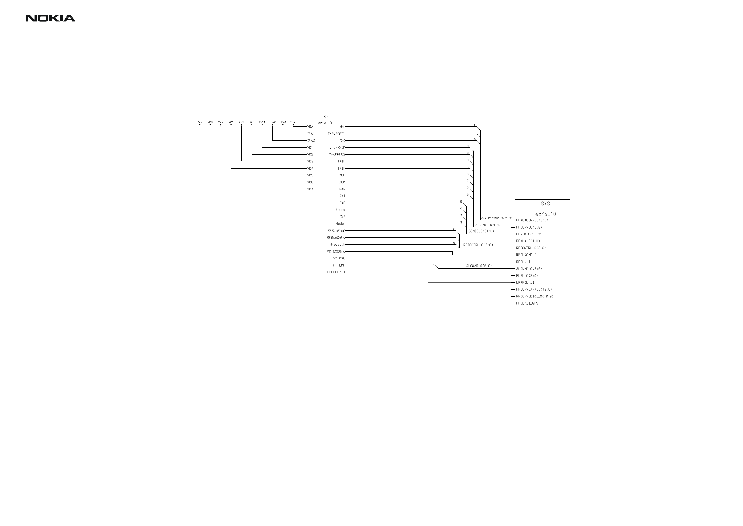
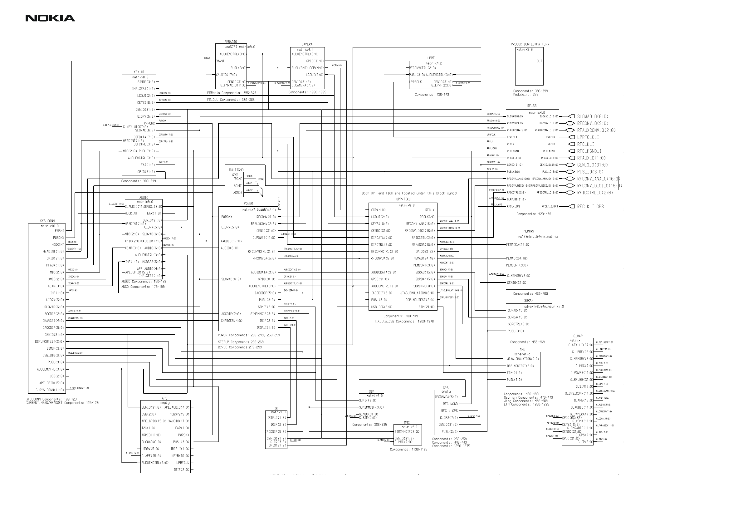
RF Top Level, v. 0.0, ed. 59
Issue 1 02/04 Copyright Nokia 2003. All rights reserved. Page A-2
Page 3
CCS Technical Documentation Schematics RH-12/RH-28
c 2
(3
Print
Edit
V.Drw.Proj
m
p-
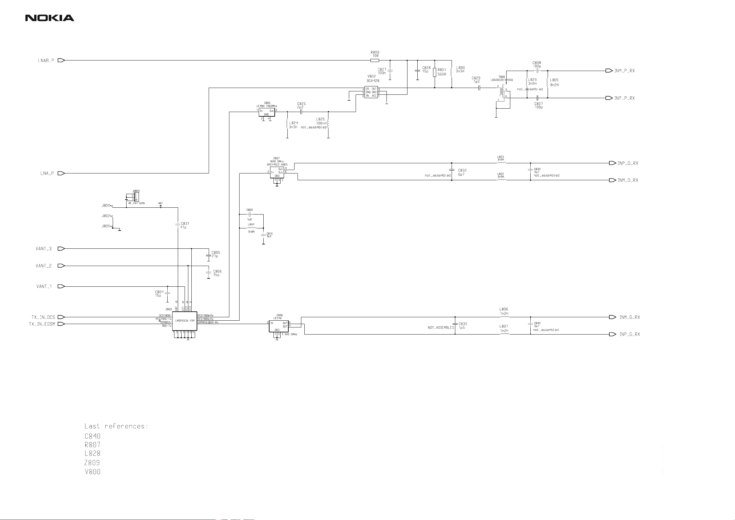
RX Front End and Antenna Switch, v. 0.0, ed. 75
Copyright (C) Nokia Corporation. All rights reserved.
THIS DRAWING IS PROTECTED BY COPYRIGHT AS AN UNPUBLISHED WORK.
UNAUTHORIZED REPRODUCTION OF THIS DRAWING IS NOT PERMITTED.
THIS DRAWING CONTAINS PROPRIETARY AND CONFIDENTIAL INFORMATION.
This document is property of Nokia Corporation
Name
RX front end and antenna switch
Assoc
RF module
Design
ez4a_10 (X.X)
Page
/RF/FRONT_END - matrix4.2 - sheet1 3
ViewPoint
pcb_design_vpt vip 18 De
Appr
Des.
KL
Dr.
Sheet of
dd-mm
21-Se
Issue 1 02/04 Copyright Nokia 2003. All rights reserved. Page A-3
Page 4
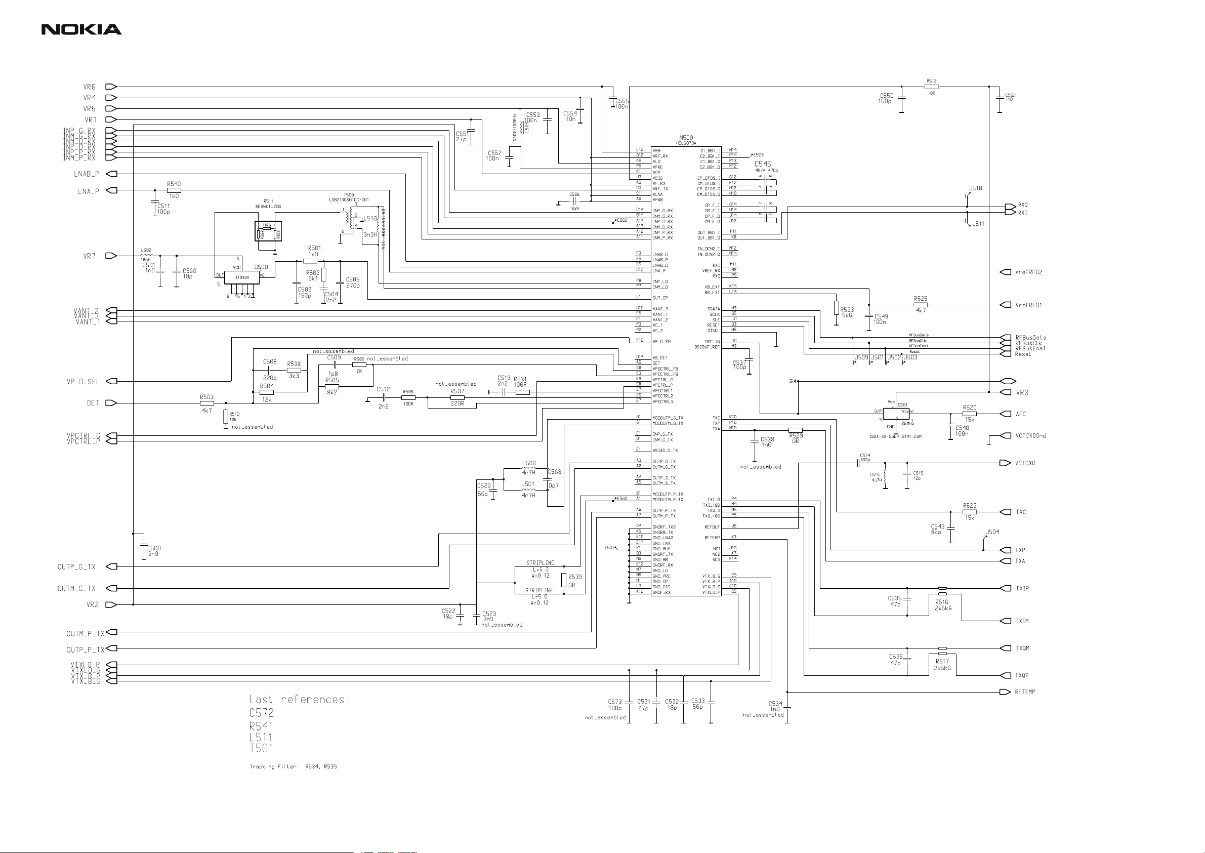
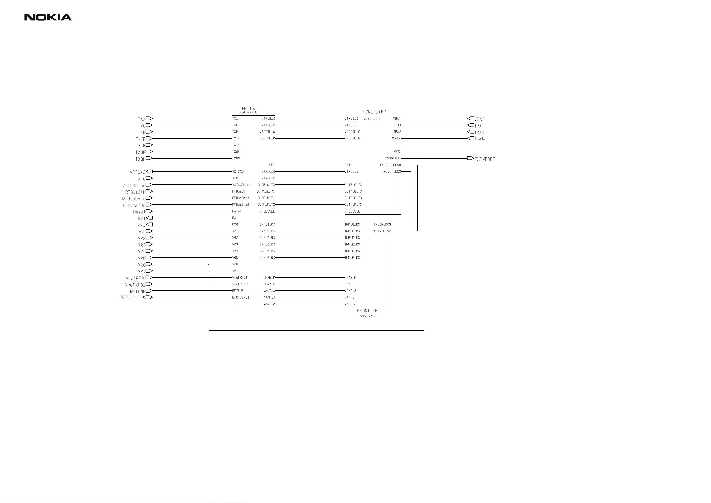
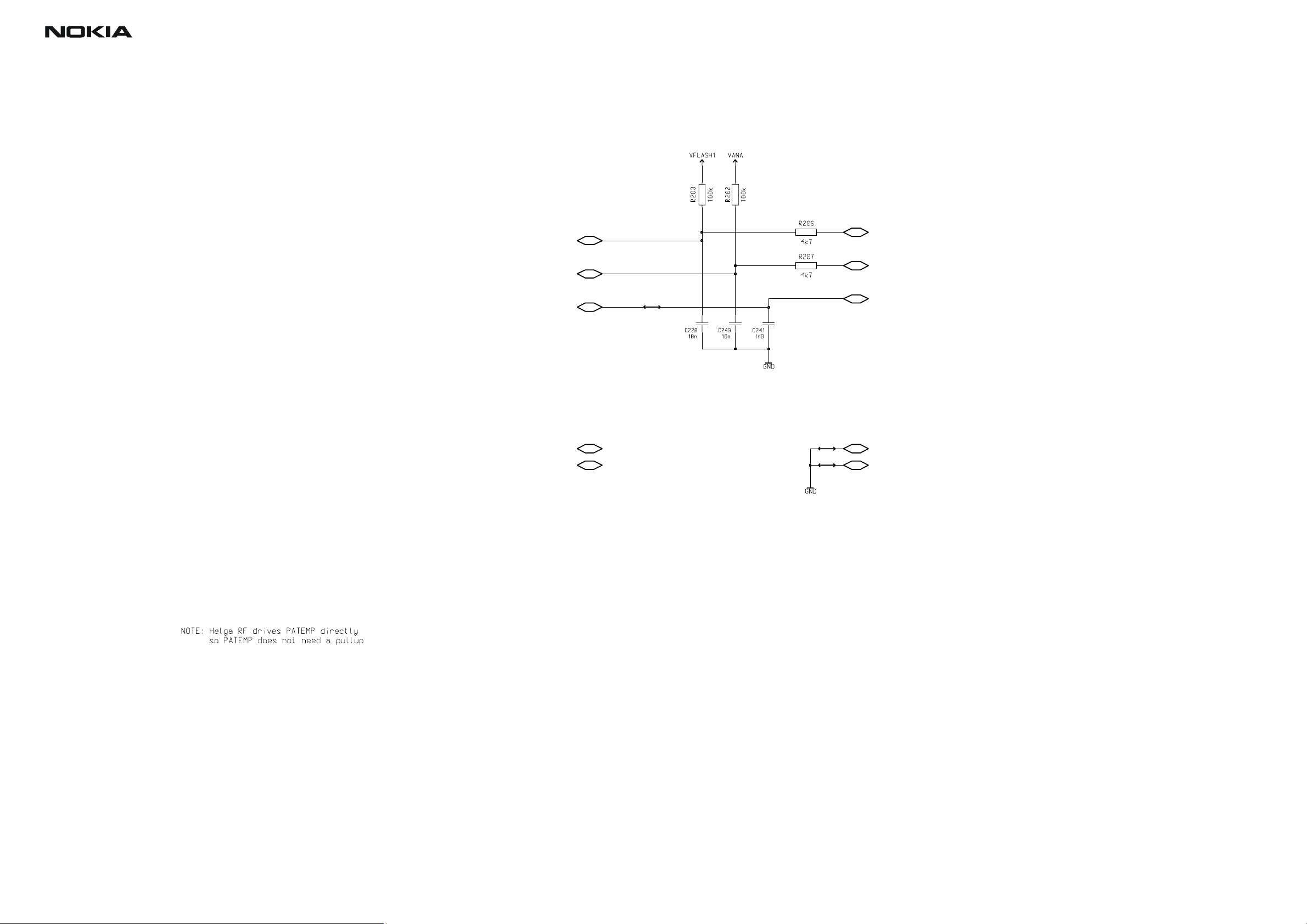
HELGA
yy
CCS Technical Documentation Schematics RH-12/RH-28
LPRFCLK_I
Copyright (C) Nokia Corporation. All rights reserved.
THIS DRAWING IS PROTECTED BY COPYRIGHT AS AN UNPUBLISHED WORK.
UNAUTHORIZED REPRODUCTION OF THIS DRAWING IS NOT PERMITTED.
THIS DRAWING CONTAINS PROPRIETARY AND CONFIDENTIAL INFORMATION.
Name
HELGA
Assoc
RF module
File
$comrf/hde12/ez4a_09/HELGA
Appr
Des.
KL
Dr.
VIP
Sheet of
xx
yy
dd-mmm-
21-Sep-99
27-Nov-03
1(01)
Issue 1 02/04 Copyright Nokia 2003. All rights reserved. Page A-4
Page 5
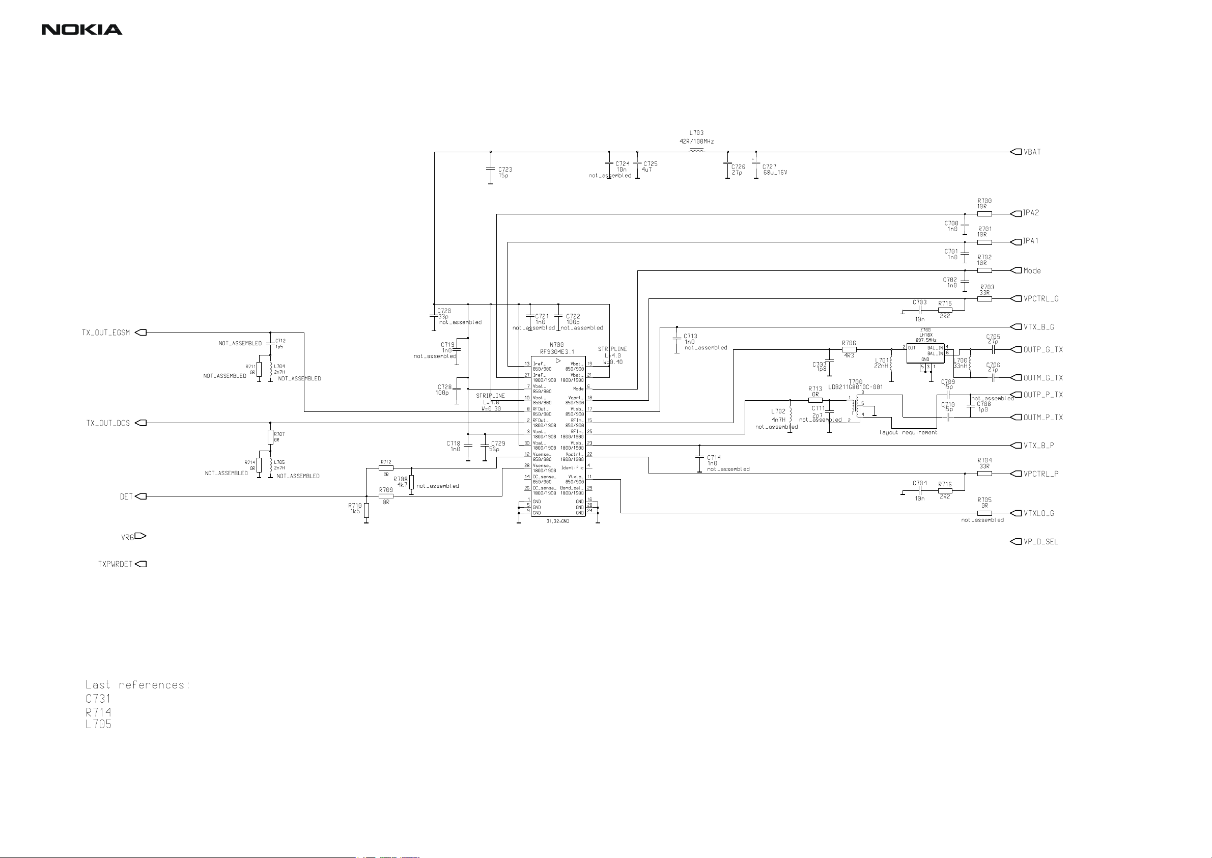
CCS Technical Documentation Schematics RH-12/RH-28
RF9204 Power Amplifier and Power Detection, v. 0.2, ed. 63
Issue 1 02/04 Copyright Nokia 2003. All rights reserved. Page A-5
Page 6
CCS Technical Documentation Schematics RH-12/RH-28
Copyright (C) Nokia Corporation. All rights reserved.
BR4.5 Top Level, v. 6.1, ed. 29
Name
BR4.5 Top level for release 6.1
Appr
dd-mmm-yy
Issue 1 02/04 Copyright Nokia 2003. All rights reserved. Page A-6
Page 7
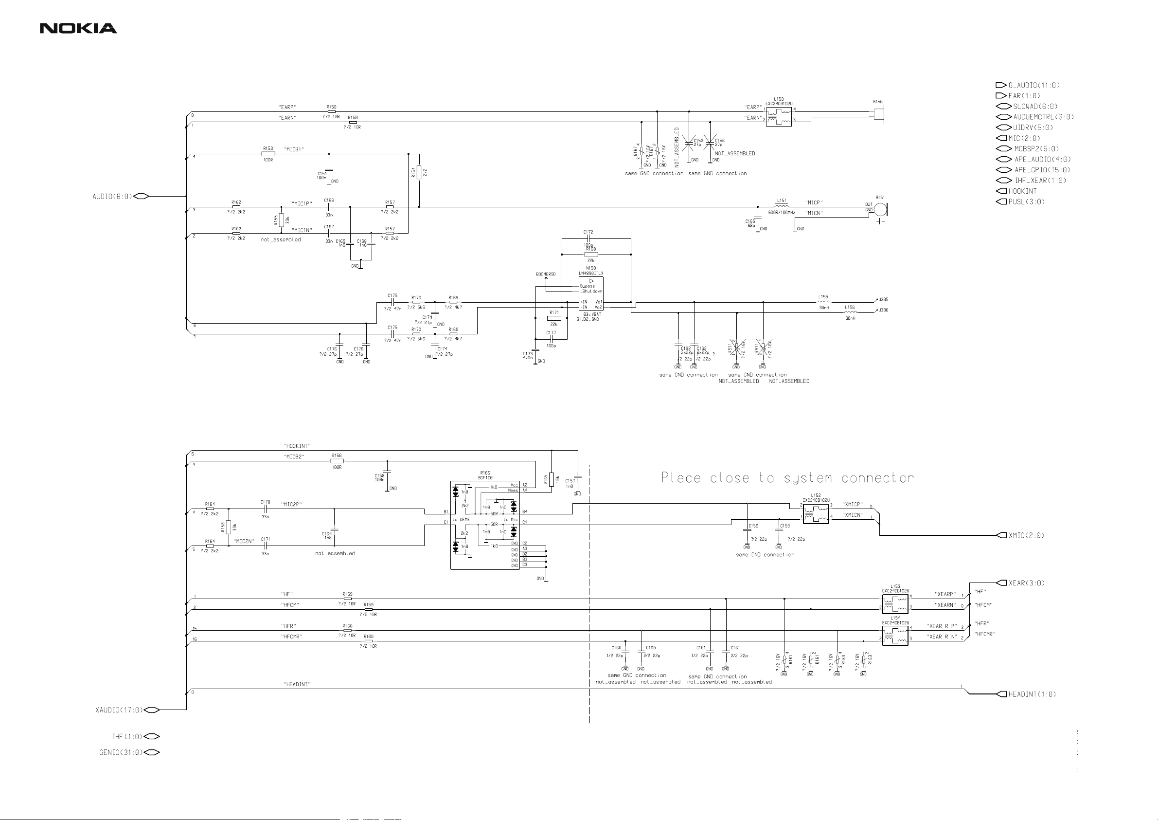
CCS Technical Documentation Schematics RH-12/RH-28
00
)
00
-yy
BR45 Audio, v. 1.6, ed. 167
IHF speaker connection
Copyright (C) Nokia Corporation. All rights reserved.
THIS DRAWING IS PROTECTED BY COPYRIGHT AS AN UNPUBLISHED WORK.
UNAUTHORIZED REPRODUCTION OF THIS DRAWING IS NOT PERMITTED.
THIS DRAWING CONTAINS PROPRIETARY AND CONFIDENTIAL INFORMATION.
This document is property of Nokia Corporation
Name
Br45 Audio
Assoc
DCT45 Common Baseband
Design
ez4a_10 (X.X)
Page
/SYS/AUDIO - matrix9.0 - sheet1 7 (39
ViewPoint
pcb_design_vpt vip 18 Dec 2
Appr
Des.
Keith Winfield
Dr.
Sheet of
dd-mmm
01-Jan-2
Issue 1 02/04 Copyright Nokia 2003. All rights reserved. Page A-7
Page 8
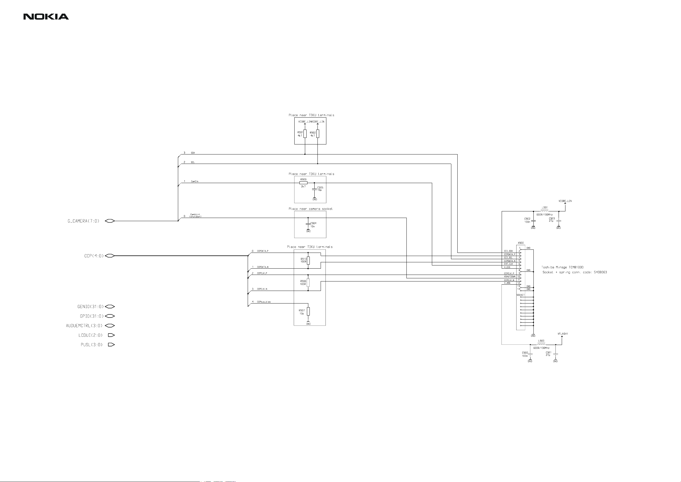
CCS Technical Documentation Schematics RH-12/RH-28
Mirage 2 VGA Camera, v. 1.1, Ed. 194
Issue 1 02/04 Copyright Nokia 2003. All rights reserved. Page A-8
Page 9
CCS Technical Documentation Schematics RH-12/RH-28
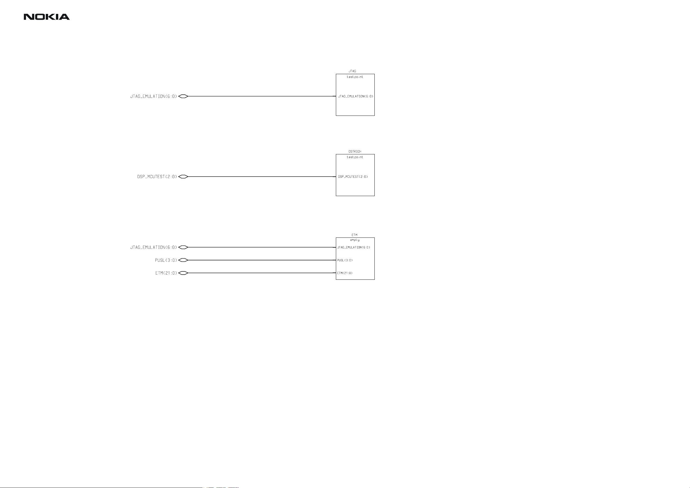
Test and Emulator Interface, v. 2.0, ed. 41
Issue 1 02/04 Copyright Nokia 2003. All rights reserved. Page A-9
Page 10
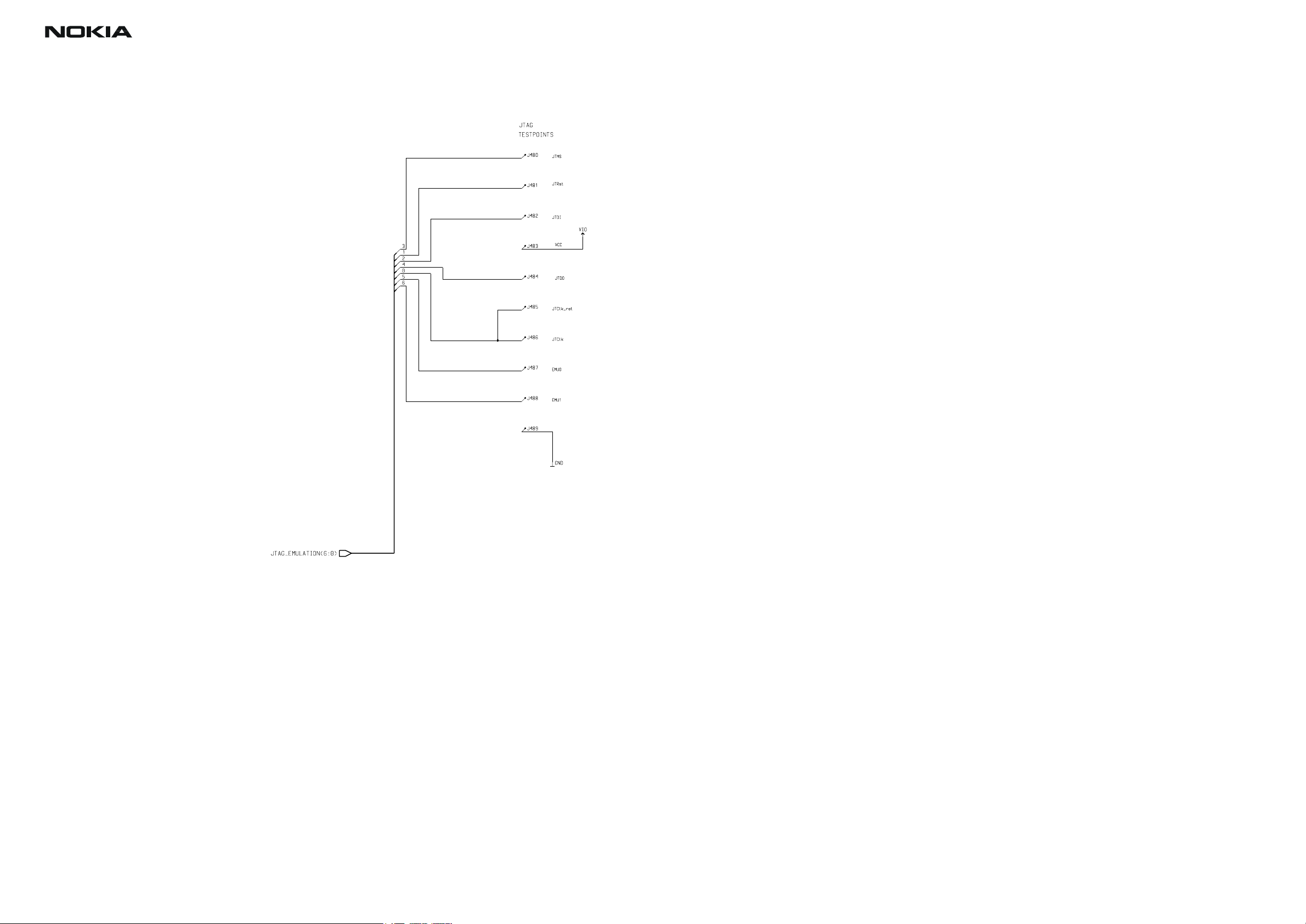
CCS Technical Documentation Schematics RH-12/RH-28
Testpoints for JTAG Emulator, v. 1.3, ed. 12
Issue 1 02/04 Copyright Nokia 2003. All rights reserved. Page A-10
Page 11
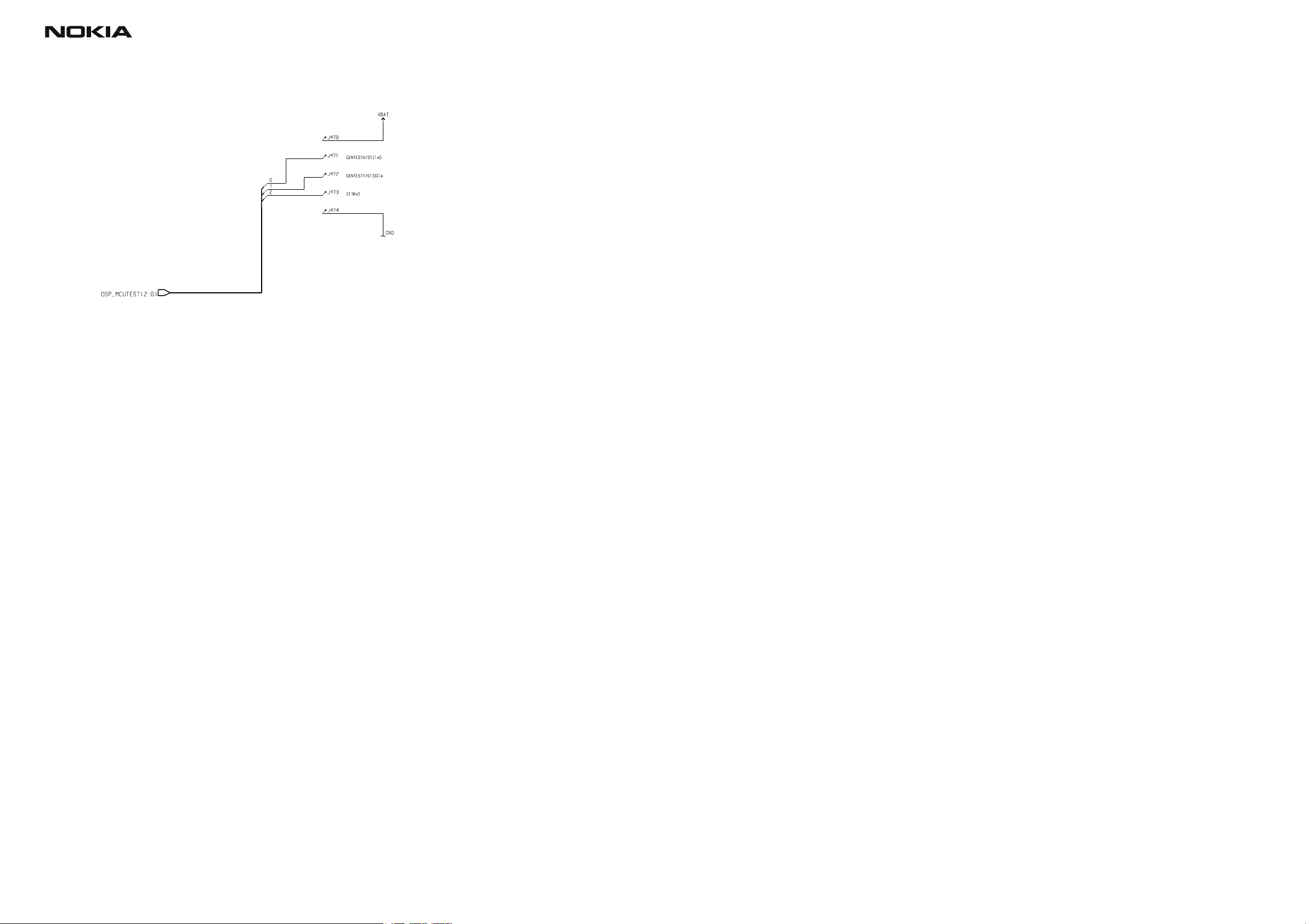
CCS Technical Documentation Schematics RH-12/RH-28
Testpoints Based Ostrich Interface, v.1.3, ed. 12
Issue 1 02/04 Copyright Nokia 2003. All rights reserved. Page A-11
Page 12
CCS Technical Documentation Schematics RH-12/RH-28
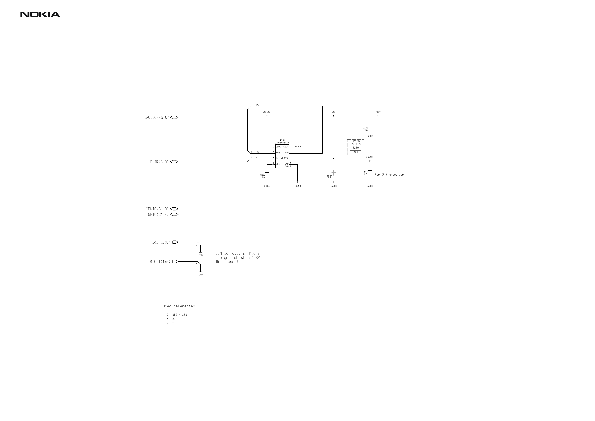
Citizen IR Module 1.8V, v. 6.1.8, ed. 55
Issue 1 02/04 Copyright Nokia 2003. All rights reserved. Page A-12
Page 13

CCS Technical Documentation Schematics RH-12/RH-28
IR Resistor 1210, v. 0, ed. 6
RES_IN RES_OUT
Issue 1 02/04 Copyright Nokia 2003. All rights reserved. Page A-13
Page 14

CCS Technical Documentation Schematics RH-12/RH-28
Key UI, v. 1, ed. 326
Issue 1 02/04 Copyright Nokia 2003. All rights reserved. Page A-14
Page 15

CCS Technical Documentation Schematics RH-12/RH-28
Flash Memory 128 Mbit, v. 2.0, ed. 74
Issue 1 02/04 Copyright Nokia 2003. All rights reserved. Page A-15
Page 16
CCS Technical Documentation Schematics RH-12/RH-28
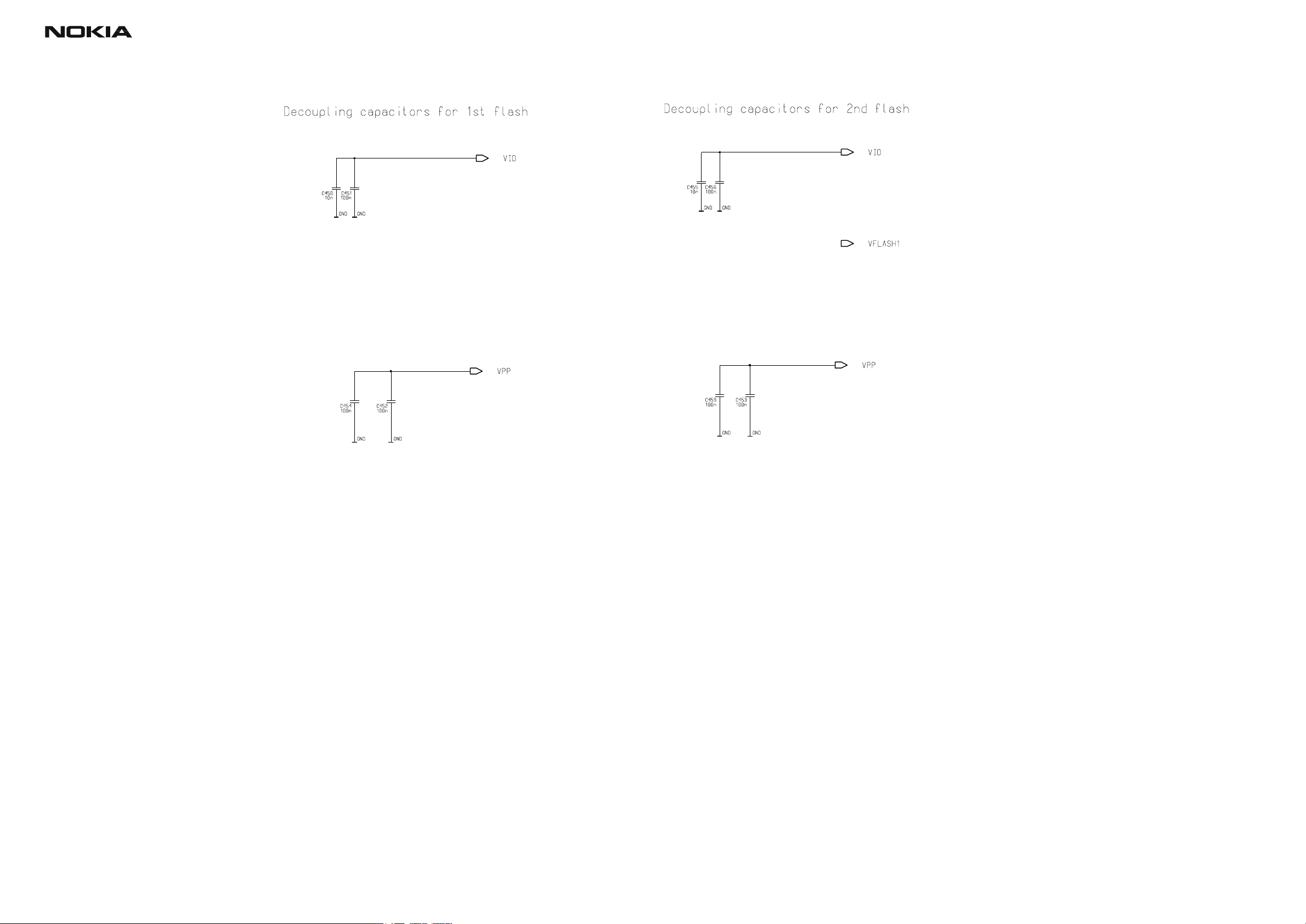
Discrete Capacitors for two Memories without VFlash1, v. 1.3, ed.11
Issue 1 02/04 Copyright Nokia 2003. All rights reserved. Page A-16
Page 17
CCS Technical Documentation Schematics RH-12/RH-28
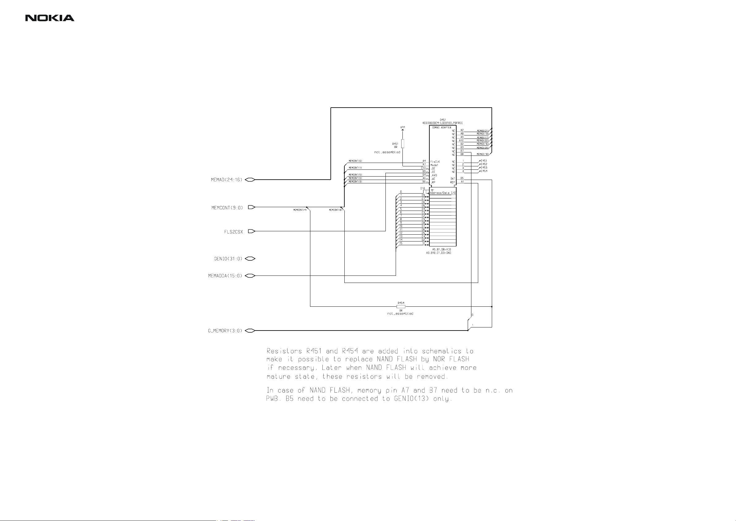
Flash Memory 64 Mbit NAND, v. 2.0, ed. 62
Issue 1 02/04 Copyright Nokia 2003. All rights reserved. Page A-17
Page 18
CCS Technical Documentation Schematics RH-12/RH-28
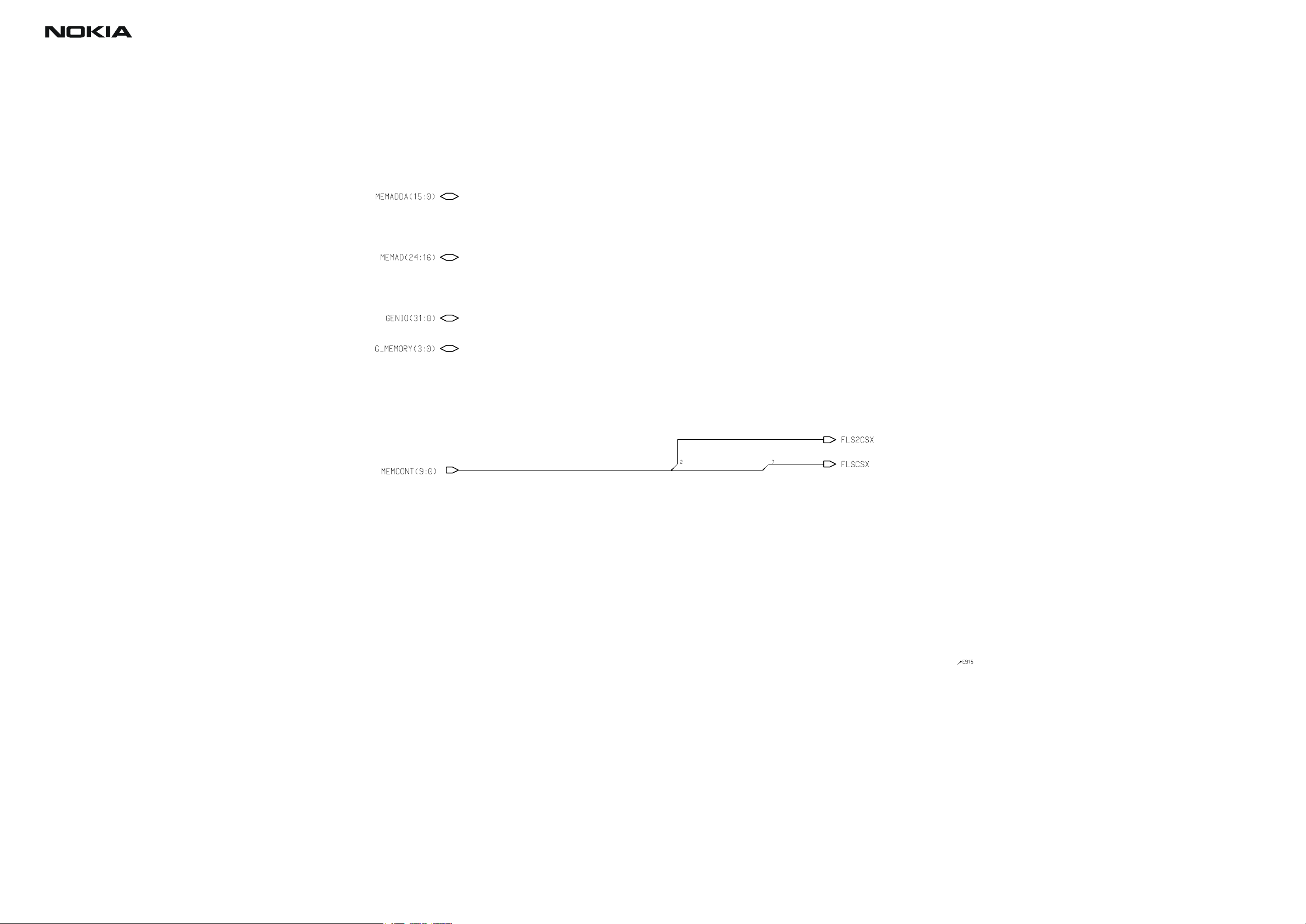
Empty Wing Sheet, v. 0, ed. 10
Issue 1 02/04 Copyright Nokia 2003. All rights reserved. Page A-18
Page 19
CCS Technical Documentation Schematics RH-12/RH-28
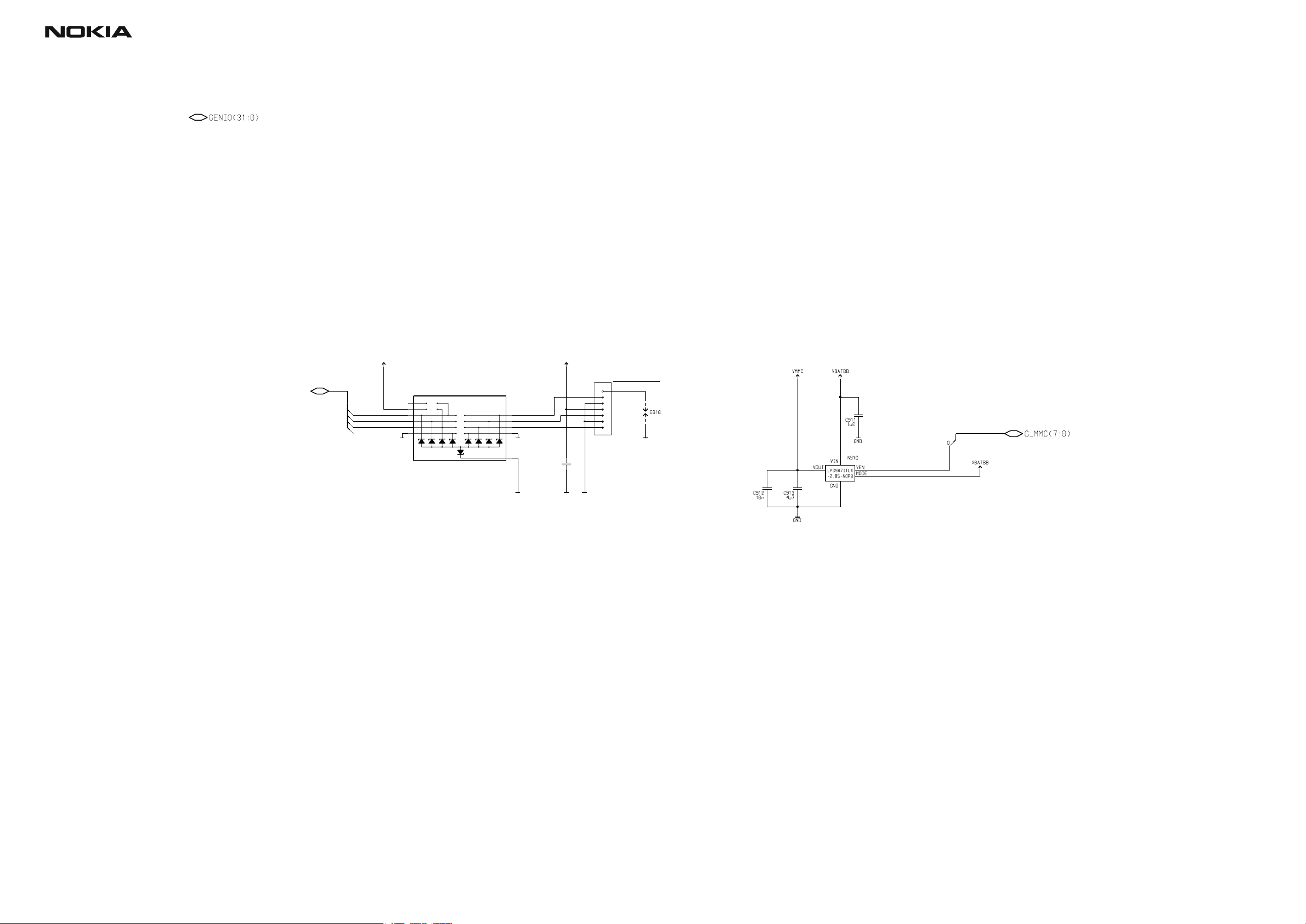
MMC Interface, v. 2.1, ed. 79
SIM2MMCIF(3:0)
VMMC
R910
EMIF04-MMC02F2
R10
1
cmd
0
clk
2
data
3
R20
R1
R2
R3
R4
NOTE: The MMC specification imposes the following impedance limits
Command pullup resistance 4.7k to 100k
Data pullup resistance 50k to 100k
EMIF02-MMC R10=13k (therefore only suitable for command line)
EMIF02-MMC R20=56k (therefore only suitable for data line)
EMIF02-MMC R1/R2/R3/R4=47R
UEME includes a 13k pullup between GEN28IO2 (command) and VAUX1
so EMIF02-MMC R10 is left unconnected. UEME has no pullup on GEN28IO3 (MMC data)
GND
GNDGND
GND
cmd
clk
data
C910
100n
VMMC
GND GND
MMC Card Connections
X910
reserved
1
2
command
3
ground
4
+ve supply
5
clock
6
ground
7
data
Not final connector
GND
ON / OFF CONTROL
1 = active / 0 = Shutdown
Power Mode
1 = Active / 0 = Sleep(3mA MAX)
Issue 1 02/04 Copyright Nokia 2003. All rights reserved. Page A-19
Page 20
CCS Technical Documentation Schematics RH-12/RH-28
UEME Power Management - Dual 1 uF 6V3 Capacitors, v 1.0, ed. 307
C202
10n
MMCClkSIM2Clk
MMCCmd/SIM2Data
MMCCmdDir/SIM2IOCtrl
MMCDataDir
MMCData
MMCData/SIM2Reset
MMCcmd/SimData
MMCClk/SimClk
MMCClkSIM2Clk
AuxDet
MMCCmdDir/SIM2IOCtrl
MMCCmd/SIM2Data
MMCDataDir
MMCData
Issue 1 02/04 Copyright Nokia 2003. All rights reserved. Page A-20
Page 21
CCS Technical Documentation Schematics RH-12/RH-28
UEME ADC Filter Block - BSI, BTEMP and Active PATEMP, v. 1.0
BSI_IN
BTEMP_IN
PATEMP_IN
VCXOTEMP_IN
BSI_OUT
BTEMP_OUT
PATEMP_OUT
LS_OUTLS_IN
VCXOTEMP_OUT
Issue 1 02/04 Copyright Nokia 2003. All rights reserved. Page A-21
Page 22
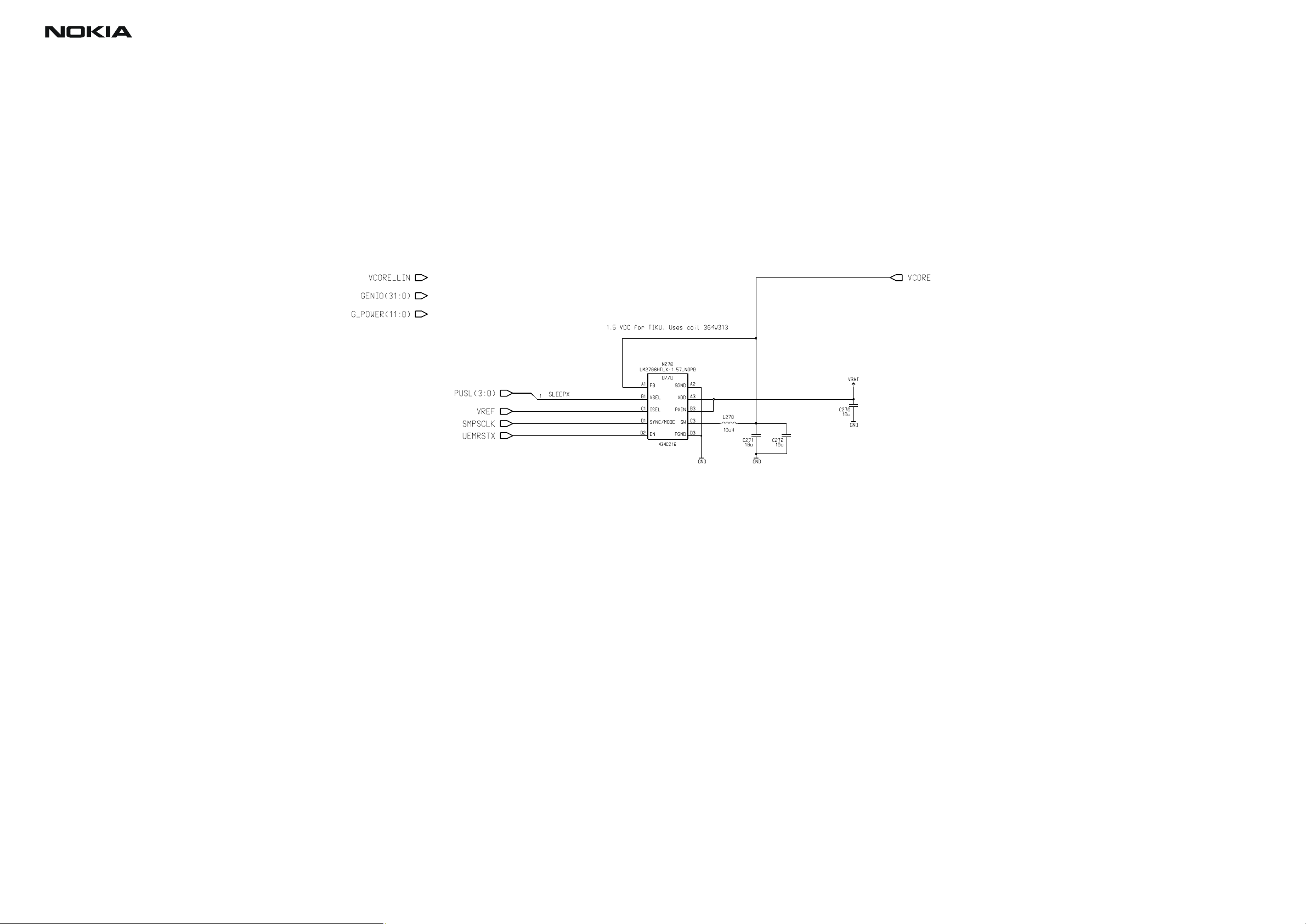
CCS Technical Documentation Schematics RH-12/RH-28
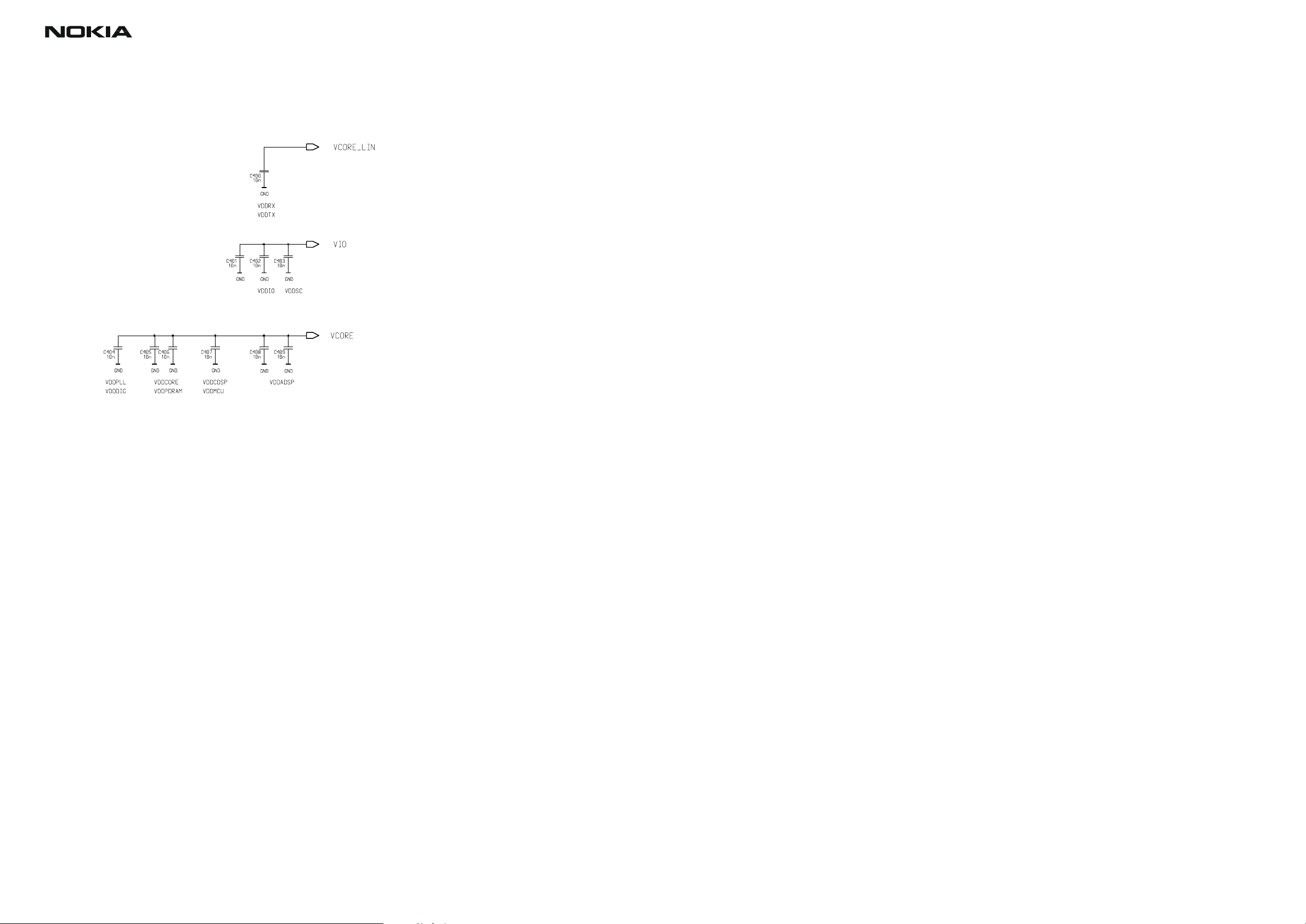
DC_DC for TIKU and VIO, v. 1.7, ed. 75
Issue 1 02/04 Copyright Nokia 2003. All rights reserved. Page A-22
Page 23
CCS Technical Documentation Schematics RH-12/RH-28
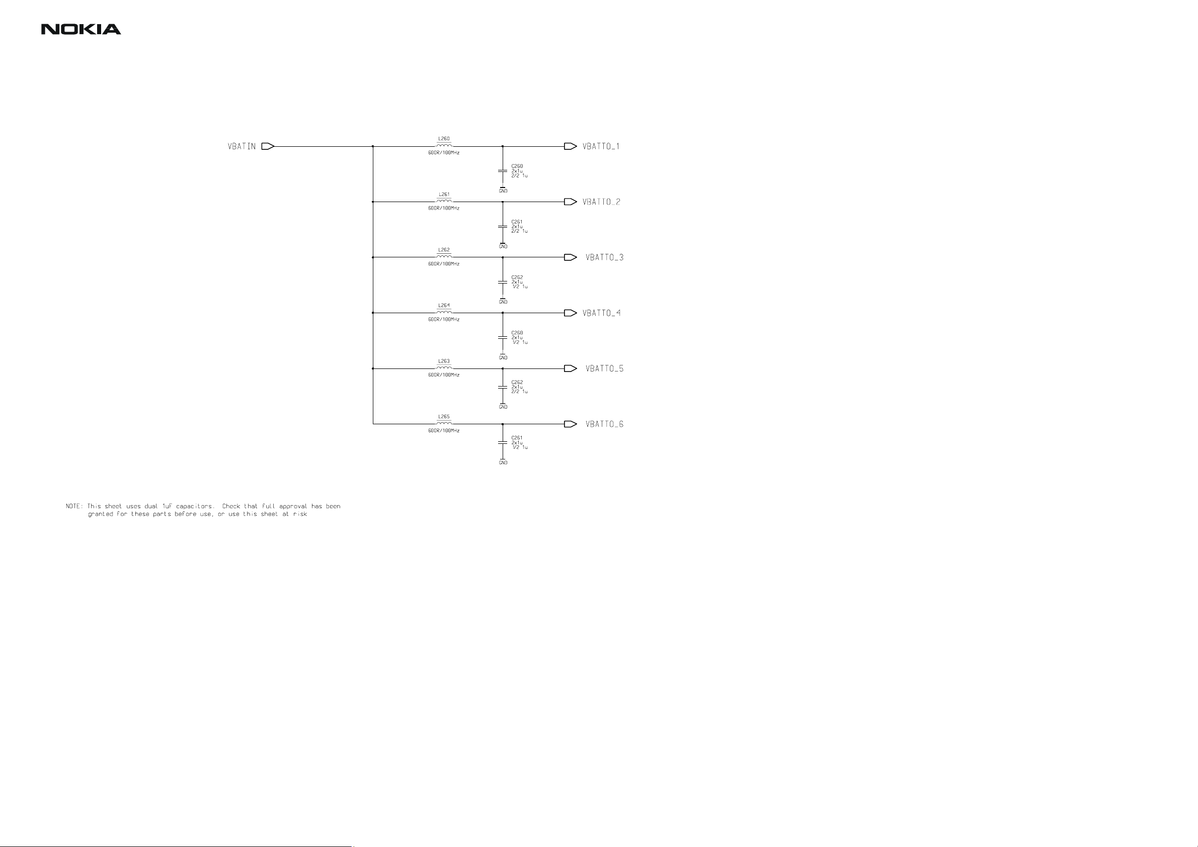
Light Filtering for Projects using 1uF Caps, v. 1.0
Issue 1 02/04 Copyright Nokia 2003. All rights reserved. Page A-23
Page 24
CCS Technical Documentation Schematics RH-12/RH-28
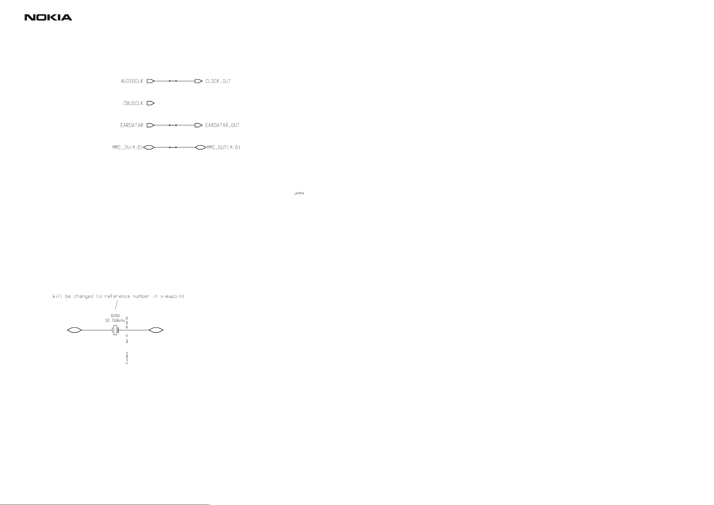
Digital-ASIC-dependent Signal Routing - TikuXX Systems, v. 1.0
32KHz Crystal - Micro Crystal CC4VT2, v. 0, ed. 6
BA
Issue 1 02/04 Copyright Nokia 2003. All rights reserved. Page A-24
Page 25
CCS Technical Documentation Schematics RH-12/RH-28
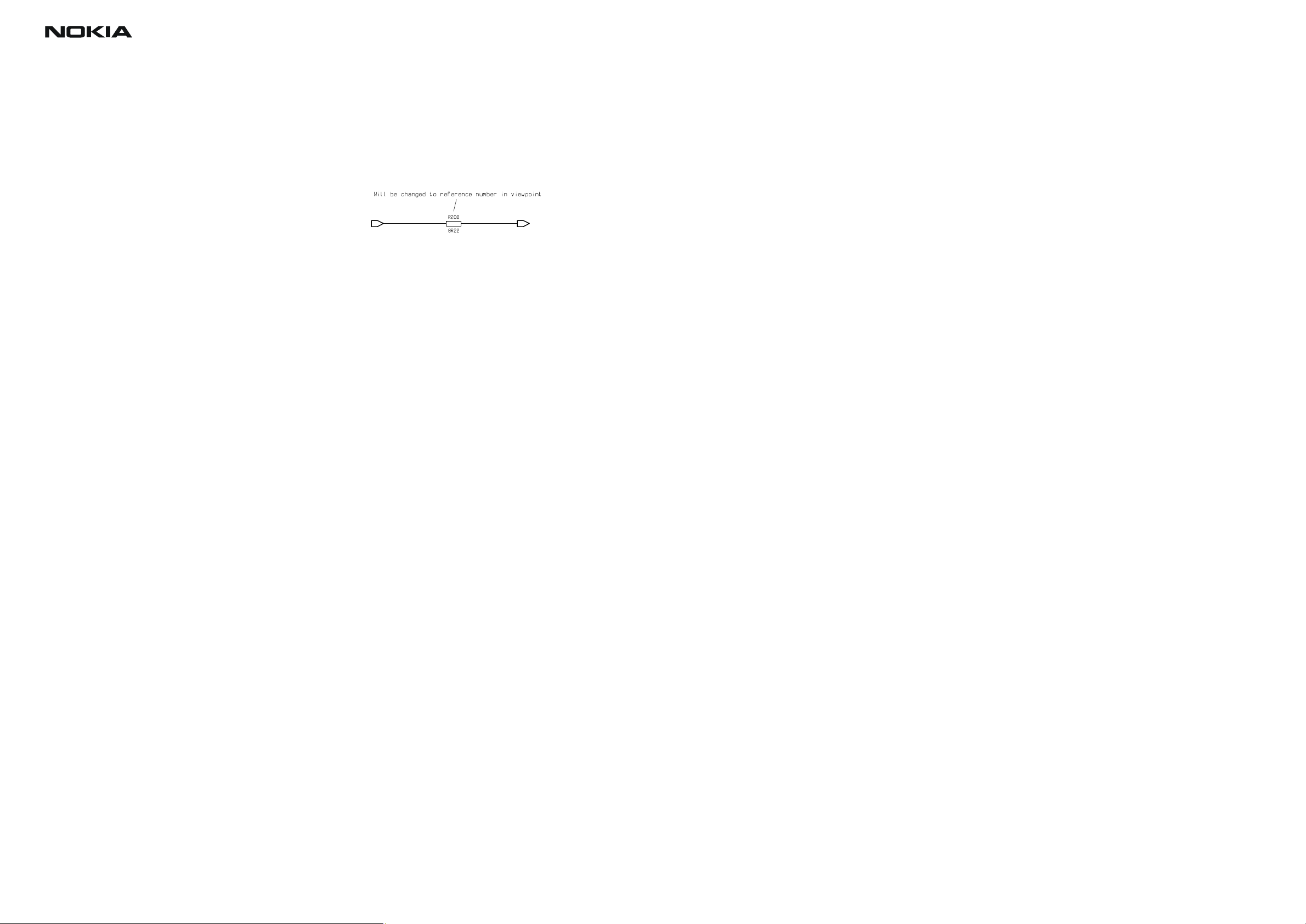
PWR Resistor 1210, v. 0, ed. 4
RES_OUTRES_IN
Issue 1 02/04 Copyright Nokia 2003. All rights reserved. Page A-25
Page 26

CCS Technical Documentation Schematics RH-12/RH-28
GSM RF - Baseband Interface, v. 1.3, ed. 64
Issue 1 02/04 Copyright Nokia 2003. All rights reserved. Page A-26
Page 27

CCS Technical Documentation Schematics RH-12/RH-28
64Mbit 1V8 SDRAM Memory, v. 1.0, ed. 64
Issue 1 02/04 Copyright Nokia 2003. All rights reserved. Page A-27
Page 28

CCS Technical Documentation Schematics RH-12/RH-28
SIM Reader, v. 1.3, ed. 66
Issue 1 02/04 Copyright Nokia 2003. All rights reserved. Page A-28
Page 29

CCS Technical Documentation Schematics RH-12/RH-28
System Connector, v. 0.0, ed. 196
X100
PUSL(3:0)
AUDUEMCTRL(3:0)
GND
GND
For After Sales
J100
J101
VBAT
J360
VBATTRF
GND
C100
27p
C101
1n0
GND
Temperature sensor
GND
R100
47k
BTEMP
RFAUX(1:0)
UIDRV(5:0)
PRODTP7
0
BSI
1
Mbus
01
PRODTP2
FbusTx
DAI_CLK
PRODTP3
FbusRx
2
DAI
0
HOOKINT
PWRONX
IACCDIF(5:0)
SIMIF(3:0)
MIC(2:0)
ACCDIF(2:0)
GENIO(31:0)
DSP_MCUTEST(2:0)
X102
1
2
3
4
5
6
7
8
9
10
11
12
13
14
GND
AGND
charge
charge gnd
ACI
Vout
Vbus
D+
Ddata gnd
Xmicn
Xmicp
Xearn
Xearp
Xear r n
Xear r p
Fbus RX
Fbus TX
CURRENT_MEAS components: 120 - 129
1+
2
GND
X101
VFLASH1
100k
R101
600R/100MHz
L102
600R/100MHz
C108
100n
L104
VAUX2
L105
1.5A
F100
Vbus
GND
GND
L100
42R/100MHz
GND
GND
GND
C102
10n
R107
EMIF02-USB02F2
C103
27p
IHF(1:0)
SLOWAD(6:0)
0
VCharln
2
Gnd
CHARGER(4:0)
HEADINT(1:0)
VIO
N100
CP2137
7
VCC_I/O
14
VCC
15
Vpu
10
D+/RXD
9
D-/TXD
_SPEED
SEMODE
SOFTCON
VP/FRX
FSE0/FTX
SUSPND
GND17=
Vreg
_OE
RCV
VM
VO
GND
GND GND
1
0
C105
10n
R4
R3
R2
R1
J104
J105
J106
HFCM
HF
HFCMR
HFR
C109
/2 1u?
GND
XMICN
XMICP
0
1
2
3
13
8
6
16
1
2
4
3
12
11
5
VAUX3
C109
? /2 1u
GND
NUT_Speed/SEM
USBPuEn
USB6Z
USBRx
USBRxM
USBRxP
USBSE
USBTx
USBSuspend
J107
J108
J109
J110
J111
J112
J113
GND
G_SYS_CONN(11:0)
17
0
5
2
1
0
4
3
18
USB_DIG(6:0)
XMIC(2:0)
XEAR(3:0)
GPIO(31:0)
GND
GND
GND
GND
GND
GND
FMANT
Issue 1 02/04 Copyright Nokia 2003. All rights reserved. Page A-29
Page 30

CCS Technical Documentation Schematics RH-12/RH-28
Current Measure, v. 0, ed. 18
VBAT
ZOCUSINT
5 pin Production Test Pattern, v. 2.0, ed. 52
2k2
GND
R121
C120
1u0
N120
LM3820TLX_NOPB
BATTERY_TERMINAL
2k2
R122
AUDUEMCTRL(3:0)
VIO
1
3
2
SLEEPCLK
Issue 1 02/04 Copyright Nokia 2003. All rights reserved. Page A-30
Page 31

CCS Technical Documentation Schematics RH-12/RH-28
)
TIKUedge Implementation (GSM)
DCT4.0
TXP
AudioClk
BOM_detect(0)
LCD Reset
Edge Mode
TXA
GENIO(31:0)
FMClk
BOM_detect(1)
Helga Reset
Reserved GPS module
GPIO(63:32)
ETM(21:0)
Reserved GPS module
BT UART CTS
BT Wake-up
BT_ResetB
BT Host Wake-up
NUT SEMode
Reserved GPS module
USB Suspend
Ext VPPEnX
USBPuEn
MEMCONT(9:0)
AUDIODATA(3:0
ExtVPPEnX
CamClk
BT UART TX
BT UART RX
BT UART RTS
IrDa SD
Eija_Interrupt
SDA (I2C) Cam
Cam Enable
SCL (I2C) Cam
KEYB(10:0)
IACCDIF(5:0)
keyboard
IrDa Rx
(Ext USBClk (48MHz))
IrDa Tx
EARDATAR
keyboard
keyboard
keyboard
keyboard
keyboard
keyboard
keyboard
keyboard
keyboard
keyboard
keyboard
keyboard
MMC Data
MMC Clk
MMC Cmd
MMC Data Dir
MMC Cmd Dir
FMCtrlDa
LCDTear
FMWrEn
FMCtrlClk
/MMC_reg_on
(Ext USBClk Enable)
BT PCM out
BT PCM Clk
BT PCM in
SDRDA(15:0)
BT PCM sync
SDRAD(15:0)
SDRCTRL(8:0)
SDRAM CSX
MEMADDA(15:0)
Net_length max=25mm
MEMAD(24:16)
Net_length max=25mm
MEMCONT(9:0)
Net_length max=25mm
DIFCTRL(3:0)
DIFDATA(7:0)
FCI Enable
FCI Int
FCI_I2C_SCL
FCI_I2C_SDA
RFCLK
PUSL(3:0) GPIO(31:0)
RFCONVDA(5:0)
TAG_EMULATION(6:0)
RFCONVCTRL(2:0)
AUDIODATA(3:0)
AUDUEMCTRL(3:0)
RFICCTRL(2:0)
LCDUI(2:0)
DSP_MCUTEST(2:0)
USB_DIG(6:0)
GENIO(31:0)
IACCDIF(5:0)
CCP(4:0)
FCONV_ANA(16:0)
FCONV_DIGI(16:0)
Issue 1 02/04 Copyright Nokia 2003. All rights reserved. Page A-31
Page 32
CCS Technical Documentation Schematics RH-12/RH-28
Discrete Decoupling Capacitors for Tiku, v. 0, ed. 12
Issue 1 02/04 Copyright Nokia 2003. All rights reserved. Page A-32
Page 33
CCS Technical Documentation Schematics RH-12/RH-28
TikuEDGE Bus Conversion Sheet, v. 1.2, ed. 102
AudioClk
FlsVppLock
EARDATAR
USBCLK
SIMCLK
SIMIOCtrl
SIMDa
HARD WIRED TO TIKU
SIM CARD I/O’s
Issue 1 02/04 Copyright Nokia 2003. All rights reserved. Page A-33
Page 34
CCS Technical Documentation Schematics RH-12/RH-28
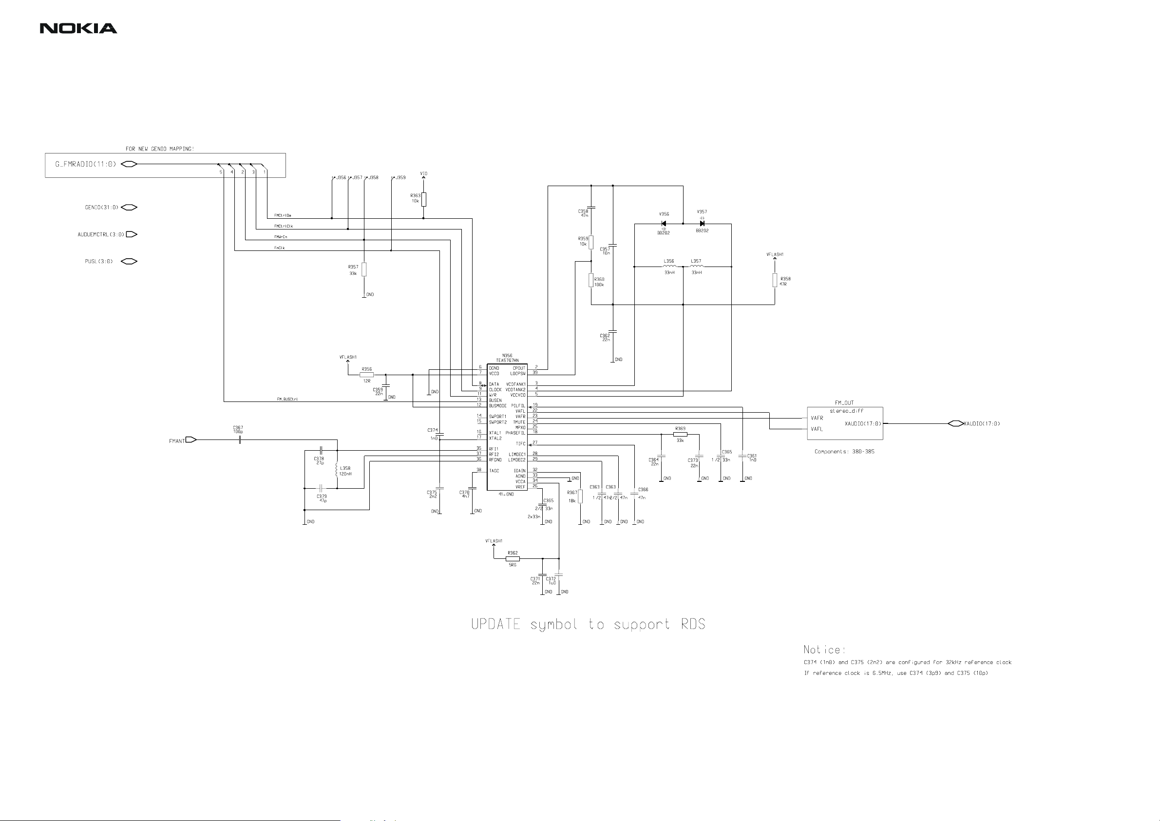
FM Radio Unit, v. 1.3, ed. 198
Issue 1 02/04 Copyright Nokia 2003. All rights reserved. Page A-34
Page 35
CCS Technical Documentation Schematics RH-12/RH-28
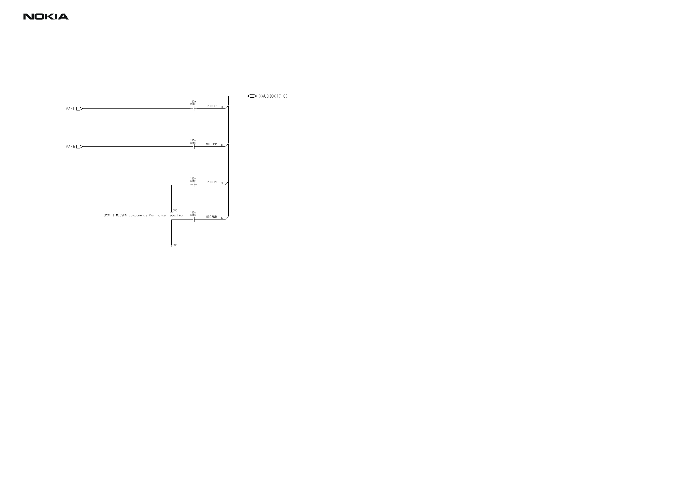
Differential Stereo. v. 0.0, ed. 7
Issue 1 02/04 Copyright Nokia 2003. All rights reserved. Page A-35
Page 36
CCS Technical Documentation Schematics RH-12/RH-28
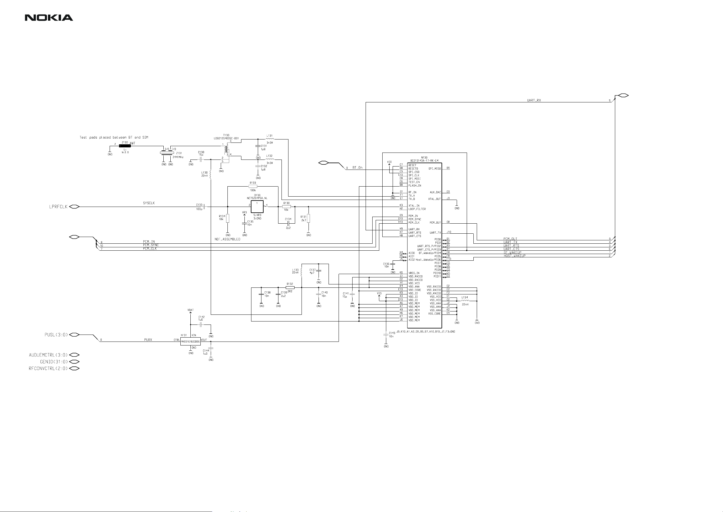
Low Power RF Module
G_LPRF(23:0)
G_LPRF(23:0)
G_LPRF(23:0)
Issue 1 02/04 Copyright Nokia 2003. All rights reserved. Page A-36
Page 37

CCS Technical Documentation Schematics RH-12/RH-28
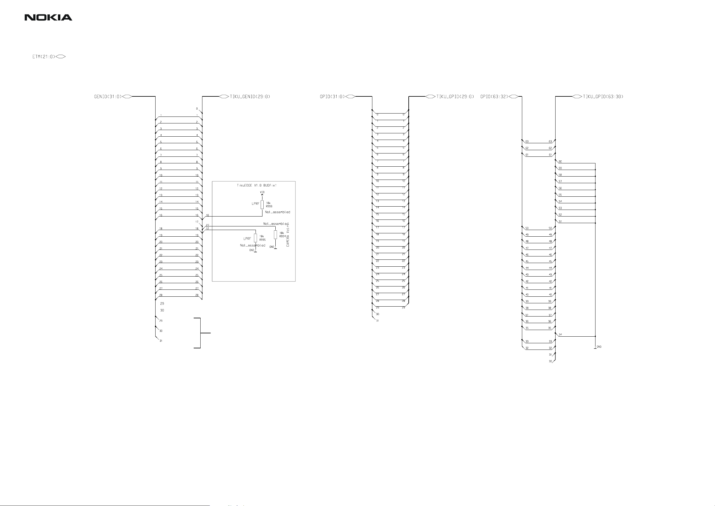
GENIO and GPIO Connection Block, v. 0.0, ed. 38
GPIO(31:0)
KEYB(10:0)
G_KEY_UI(67:0)
G_AUDIO(11:0)
G_APE(15:0)
G_CDMA(11:0)
GPIO(63:32)
IrDa Rx
IrDa Tx
keyboard
keyboard
keyboard
keyboard
keyboard
keyboard
keyboard
keyboard
keyboard
keyboard
keyboard
keyboard
keyboard
MMC Clk
MMC Data
MMC Cmd
MMC Data Dir
MMC Cmd Dir
(Ext USBClk Enable)
LCDTear
FMWrEn
/MMC_reg_on
FMCtrlClk
FMCtrlDa
BT PCM Clk
BT PCM out
BT PCM in
BT PCM sync
FM BUSCTRL
FCI Enable
FCI Int
FCI_I2C_SCL
FCI_I2C_SDA
G_POWER(11:0)
G_FMRADIO(11:0)
G_GPS(7:0)
G_SIM(7:0)
G_MMC(7:0)
G_LPRF(23:0)
GENIO(31:0)
AudioClk
BOM_detect(0)
TXP
Edge Mode
LCD Reset
TXA
Helga Reset
BOM_detect(1)
FMClk
Reserved GPS module
Reserved GPS module
Reserved GPS module
BT Host Wake-up
BT Wake-up
NUT SEMode
BT_ResetB
BT UART CTS
Ext VPPEnX
USBPuEn
USB Suspend
BT UART RX
BT UART TX
BT UART RTS
IrDa SD
CamClk
SCL (I2C) Cam
SDA (I2C) Cam
Cam Enable
Eija_Interrupt
EARDATAR
(Ext USBClk (48MHz))
G_IR(3:0)
G_RF_BB(31:0)
G_SYS_CONN(11:0)
G_CAMERA(7:0)
PA
G_MEMORY(3:0)
BOM detect
R915 R916
Issue 1 02/04 Copyright Nokia 2003. All rights reserved. Page A-37
 Loading...