

Page 1

CCS Technical Documentation
RH-12/RH-28 Series Transceivers
7 - System Module
Issue 1 02/04 Nokia Corporation
Page 2

RH-12/RH-28
System Module CCS Technical Documentation
[This page left intentionally blank]
Page 2 Nokia Corporation Issue 1 02/04
Page 3

RH-12/RH-28
CCS Technical Documentation System Module
Table of Contents
Page No
Glossary of Terms..................................................................................................................................... 5
Baseband Module Introduction........................................................................................................... 8
Features...................................................................................................................................................... 9
Environmental Specifications............................................................................................................ 10
Normal and extreme voltages .........................................................................................................10
Temperature conditions ....................................................................................................................10
Humidity ...............................................................................................................................................11
Vibration ...............................................................................................................................................11
ESD strength ........................................................................................................................................11
Technical Specifications ..................................................................................................................... 12
UEME ......................................................................................................................................................12
DC Characteristics .......................................................................................................................... 14
Power Distribution.......................................................................................................................... 15
Tiku .........................................................................................................................................................16
Main Features.................................................................................................................................. 16
Memory Block.................................................................................................................................. 17
Memory .................................................................................................................................................17
NOR Flash.......................................................................................................................................... 17
NAND Flash....................................................................................................................................... 17
SDRAM............................................................................................................................................... 17
Charging ................................................................................................................................................18
Battery ...................................................................................................................................................20
Interfaces ..............................................................................................................................................20
FM-Radio........................................................................................................................................... 20
IrDA..................................................................................................................................................... 21
Camera............................................................................................................................................... 23
SIM...................................................................................................................................................... 25
MMC................................................................................................................................................... 26
Bluetooth .......................................................................................................................................... 27
FBUS ................................................................................................................................................... 29
USB ..................................................................................................................................................... 30
UI Interface....................................................................................................................................... 31
RF Interface ...................................................................................................................................... 36
Test Pattern ...................................................................................................................................... 36
Test Points............................................................................................................................................... 38
Main board A side of PWB ...............................................................................................................38
Main board B side of PWB ...............................................................................................................39
RF Module Introduction...................................................................................................................... 40
RF Frequency Plan ..............................................................................................................................41
DC Characteristics ..............................................................................................................................41
Regulators......................................................................................................................................... 41
Typical Current Consumption...................................................................................................... 42
Power Distribution.......................................................................................................................... 43
RF Characteristics ...............................................................................................................................43
RF Block Diagram ...............................................................................................................................46
Frequency Synthesizers................................................................................................................. 47
Receiver ............................................................................................................................................. 47
Issue 1 02/04 Nokia Corporation Page 3
Page 4

RH-12/RH-28
System Module CCS Technical Documentation
Transmitter ....................................................................................................................................... 47
Front End........................................................................................................................................... 47
Power Amplifier............................................................................................................................... 48
RF ASIC Helgo.................................................................................................................................. 49
AFC function .................................................................................................................................... 49
Antenna ............................................................................................................................................. 49
Page 4 Nokia Corporation Issue 1 02/04
Page 5

RH-12/RH-28
CCS Technical Documentation System Module
Glossary of Terms
ACI Accessory Control Interface
ADC Analog Digital Connector
AMSL After Market Service Leader
ASIC Application Specific Integrated Circuit
ASIP Application Specific Integrated Passive
ADSP Application DSP (expected to run high level tasks)
ARM Advanced RISC Machines
BB Baseband
BC02 Bluetooth module made by CSR
CCP Compact Camera Port
CDSP Cellular DSP (expected to run low level tasks)
COF Chip on foil
COG Chip On Glass
CSR Cambridge Silicon Radio
CSTN Color Super Twisted Nematic
CTSI Clock Timing Sleep and Interrupt block of Tiku
DCT4.5 Digital Core Technology, generation 4.5
DSP Digital Signal Processor
EMC Electro Magnetic Compatibility
ESD Electro Static Discharge
FCI Functional Cover Interface
FR Full Rate
FSTN Film compensated Super Twisted Nematic
Issue 1 02/04 Nokia Corporation Page 5
Page 6

RH-12/RH-28
System Module CCS Technical Documentation
GSM Global System Mobile
HW Hardware
IF Interface
IHF Integrated Hands Free
IMEI International Mobile Equipment Identity
IR Infrared
IrDa Infrared Data Association
LCD Liquid Crystal Display
LDO Low Drop Out
LED Light Emitting Diode
LPRF Low Power Radio Frequency
MCU Microprocessor Control Unit
NTC Negative temperature Coefficient, temperature sensitive resistor
used as an temperature sensor.
PA Power Amplifier (RF)
PDA Personal Digital Assistant
PDRAM Program/Data RAM (on chip in Tiku)
Phoenix SW tool of DCT4.x
PUP General Purpose IO (PIO), USARTS and Pulse Width Modulators
PWB Printed Wired Board
PopPort
TM
BB4.x system connector. It includes: USB, Stereo headset, Fbus.
RTC Real Time Clock, small circuitry that keeps track of updating the
clock counter and the calendar. To keep it update without (or
empty) battery, an alternative power source can be used: small
battery or large capacitor.
SARAM Single Access RAM
Page 6 Nokia Corporation Issue 1 02/04
Page 7

RH-12/RH-28
CCS Technical Documentation System Module
SIM Subscriber Identification Module
SW Software
SWIM Subscriber / Wallet Identification Module
SPR Standard Product Requirements
STI Serial Trace Interface
TCXO Temperature controlled Oscillator
Tiku Finnish for Chip, Successor of the UPP (Universal Phone
Processor), Official Tiku3G
UEME Universal Energy Management Enhanced
UI User Interface
USB Universal Serial Bus
UPP Universal Phone Processor
UPP_WD2 Communicator version of DCT4 system ASIC
Issue 1 02/04 Nokia Corporation Page 7
Page 8
RH-12/RH-28
System Module CCS Technical Documentation
Baseband Module Introduction
This chapter describes the baseband module for the RH-12/RH-28 program. The baseband module includes the baseband engine chipset, the UI components and acoustical
parts of the transceiver.
The RH-12/RH-28 is a hand-portable GSM900/GSM1800/GSM1900 phone for the Smart
Classic segment, having the DCT4.5 generation baseband- and RF circuitry. The key driver
for this product is the implementation of EDGE, introducing true multimedia capability
from WCDMA in GSM single mode.
RH-12/RH-28 is equipped with the DCT4 connector, supporting most of the DCT4 accessories. The battery interface is relative new consisting of only 3 connections. Standard
battery will be the BL-5C battery with 850mAh.
Page 8 Nokia Corporation Issue 1 02/04
Page 9

RH-12/RH-28
CCS Technical Documentation System Module
Features
The HW specific features of the RH-12/RH-28 phone:
• Monoblock phone with easy exchangeable covers.
• Tripleband Engine (900, 1800, 1900), US variant (850, 1800, 1900)
• E-GPRS MSC 5 (2+2)
• FR, EFR, AMR codecs
• Integrated Camera and Colour Display 128x128
• MMS (Multi Media Messaging), Java MIDP, SyncML & xHTML
• MMC for storing pictures and sound
• SWIM (dual function SIM)
• MP3 Player
• USB Interface to PC
•IrDA
• Bluetooth
•FM Radio
•IHF
• PopPort
Accessories:
• Chargers: ACP7, ACP8, ACP9, ACP-12, LCH-8, LCH-9, LCH-12, AC-1 and DC-1.
• Car accessories: CARK126, CARK112, BHF-1 and RAN CARKIT 610/810 (BT).
TM
Accessory support
• Audio accessories: HDB-4, HS-5, LPS-4, HS-10, HS-6, SU-3, HF-2, HDS-3, HDW1, HDW-2, DT-1
• Connectivity accessories: DCV-14, DKU-2, DTL-4 and HDA-10.
• Accessory covers: X-press on covers.
Issue 1 02/04 Nokia Corporation Page 9
Page 10
RH-12/RH-28
System Module CCS Technical Documentation
Environmental Specifications
Normal and extreme voltages
Following voltages are assumed as normal and extreme voltages for used battery:
Table 1: Normal and extreme voltages
Voltage Voltage [V] Condition
General Conditions
Nominal voltage 3,700
Lower extreme voltage 3,145 1
Higher extreme voltage
(fast charging)
HW Shutdown Voltages
Vmstr+ 2,1 ± 0,1 Off to on
Vmstr- 1,9 ± 0,1 On to off
SW Shutdown Voltages
Sw shutdown 3,1 In call
Sw shutdown 3,2 In idle
Min Operating Voltage
Vcoff+ 3,1 ± 0,1 Off to on
Vcoff- 2,8 ± 0,1 On to off
1
ADC settings in the SW might shutdown the phone above this value.
2
During fast charging of an empty battery, the voltage might exceed this value. Voltages between
4.20 and 4.60 might appear for a short while.
4,230 2
Temperature conditions
• Operational temperature range (all specifications met within this range):
–5°C.. +55°C (stationary use)
• Functional temperature range (reduced performance):
–30°C.. +70°C
• Storage temperature range:
–30°C.. +85°C
Temperatures at –10°C, +25°C and +55°C are used for the cpk analysis.
The baseband module complies with the SPR4 Operating Conditions.
Page 10 Nokia Corporation Issue 1 02/04
Page 11

RH-12/RH-28
CCS Technical Documentation System Module
Humidity
Relative humidity range is 5...95%.
The BB module is not protected against water. Condensed or splashed water might cause
malfunction. Any submerge of the phone will cause permanent damage. Long-term high
humidity, with condensation, will cause permanent damage because of corrosion.
The baseband module complies with the SPR4 Operating Conditions.
Vibration
The baseband module complies with the SPR4 Operating Conditions.
ESD strength
Standard for electrostatic discharge is IEC 61000-4-2 and level 4 requirements are fulfilled.
The baseband module complies with the SPR4 Operating Conditions.
Issue 1 02/04 Nokia Corporation Page 11
Page 12

RH-12/RH-28
System Module CCS Technical Documentation
Technical Specifications
UEME
UEME is the Universal Energy Management Enhanced IC for digital hand portable
phones. In addition to energy management, the UEME functionality performs all baseband mixed–signal functions.
The different states of the UEME are explained below.
No supply
In the NO_SUPPLY mode the UEME has no supply voltage (VBAT < VMSTR and
VBACK<V_BUCOFF-). This mode is due to the fact, that both the main battery and the
backup battery are either disconnected or both discharged to a low voltage level.
The UEME will recover from NO_SUPPLY into the RESET mode, if the VBAT voltage level
rises above the VMSTR+ level, by either reconnecting the main battery or charging it to
such level.
Backup
In the BACK_UP mode the main battery is either disconnected or has a low voltage level
(VBAT < VMSTR- and VBACK > V_BUCOFF+).
The regulator VRTC that supplies the real time clock is disabled in the BACK_UP mode.
Instead the unregulated backup battery voltage VBACK supplies the output of the VRTC.
All other regulators are disabled and the phone has no functionality.
The UEME will recover from the BACK_UP mode into the RESET mode if VBAT rises above
VMSTR+.
Power off
In order for the UEME to be in the PWR_OFF mode, it must have supply voltage (VBAT >
VMSTR+).
The VRTC regulator is enabled and supplying the RTC within the UEME. The UEME will
enter the RESET mode after a 20 ms delay whenever one of the below listed conditions is
logically true:
• The power button is activated.
• Charger connection is detected.
• RTC alarm is detected.
The UEME will enter PWR_OFF from all other modes except NO_SUPPLY and BACK_UP if
the internal watchdog elapses.
Page 12 Nokia Corporation Issue 1 02/04
Page 13

RH-12/RH-28
CCS Technical Documentation System Module
Reset
When the UEME enters the RESET mode from the PWR_OFF mode the watchdog is
enabled. If the VBAT fails to rise above the power-up voltage level VCOFF+ (3.1 V), before
the watchdog elapses, the UEME will enter the PWR_OFF mode. Otherwise, after a 200
ms delay the regulator VFLASH1 will be enabled and after an additional delay of 500 _s,
the regulators VANA, VIO, VCORE and VR3 will be enabled. All other regulators i.e.
VFLASH2, VSIM, VR1, VR2 and VR4 – VR7 are software controlled and disabled by
default. After an additional delay of 20 ms, the UEME enters the PWR_ON mode.
Power on
In PWR_ON the UEME is fully functional in the sense that all internal circuits are powered up or can be by means of software. The UEME will enter the PWR_OFF mode if VBAT
drops below VCOOF- for a period of time longer than 5 _s. The UEME will furthermore
enter the PWR_OFF mode if either of the watchdogs Operational State Machine (approx.
100 _s), Security (32 sec.) or Power Key (4 sec.) elapses or if any of the regulators triggers
the thermal protection circuitry.
Sleep
The UEME can be forced into the SLEEP mode by the Tiku by setting the input SLEEPX low
for more than 60 _s. This state is entered when the external Tiku activity is low (phone in
sleep) and thereby lowering the internal current consumption of the UEME. The regulator
VANA is disabled and VR1 – VR7 are either disabled or in low quiescent mode. From
SLEEP the UEME enters PWR_ON if SLEEPX goes high, the PWR_OFF mode if watchdog
elapses or the BACK_UP mode if VBAT drops below VMSTR-.
Protection mode
The UEME has two separate protection limits for over temperature conditions, one for
the charging switch and one for the regulators. The temperature circuitry measures the
onchip temperature. In case of charging over temperature, the circuit turns the charging
switch off. In case of over temperature in any of the regulators, the UEME powers off.
Issue 1 02/04 Nokia Corporation Page 13
Page 14
RH-12/RH-28
System Module CCS Technical Documentation
DC Characteristics
The figures in the following table reflect the specification of the voltage and current regulators within the UEME.
Table 2: UEME Regulator Output and State in Sleep
Voltage (V) Current (mA)
Name
Min Nom Max Max
VANA 2.70 2.78 2.86 80 2 5uA minimum for stability.
VFLASH1 2.61 2.78 2.95 70 1.5 1 5uA minimum for stability. Con-
VIO 1.72 1.80 1.88 150 0.5 3 5uA minimum for stability. Con-
VCORE 1.41 1.50 1.59 200 0.2 1 5uA minimum for stability.
VAUX1 1.745
2.91
VAUX2 2.70 2.78 2.86 70 0.5 1 5uA minimum for stability.
VAUX3 2.70 2.78 2.86 10 0.5 1 5uA minimum for stability.
VSIM 1.745
2.91
VR1A/B 4.60 4.75 4.90 10 - 4 Disabled in Sleep mode. The max-
1.80
3.0
1.80
3.00
1.855
3.09
1.855
3.09
50 0.5 1 Voltage level is set by MCUSW.
25 0.5 - 5uA minimum for stability.
Sleep
Max
Filter Comment
Controlled by the UEME. Disabled
in Sleep mode.
trolled by the UEME.
trolled by the UEME.
MCUSW is setting the voltage.
imum current is for 1 regulator
active. If both are used, maximum 5mA each.
VR2 2.70
(2.61)
VR3 2.70 2.78 2.86 20 - 4 100uA minimum for stability.
VR4 2.70 2.78 2.86 50 0.1 6 100uA minimum for stability.
VR5 2.70 2.78 2.86 50 0.1 7 100uA minimum for stability.
VR6 2.70 2.78 2.86 50 0.1 7 100uA minimum for stability.
VR7 2.70 2.78 2.86 45 - 7 100uA minimum for stability.
2.78
(2.78)
2.86
(2.95)
100 - 5 100uA minimum for stability.
Active during (Sleepmode).
Controlled by the UEME.
Page 14 Nokia Corporation Issue 1 02/04
Page 15
RH-12/RH-28
CCS Technical Documentation System Module
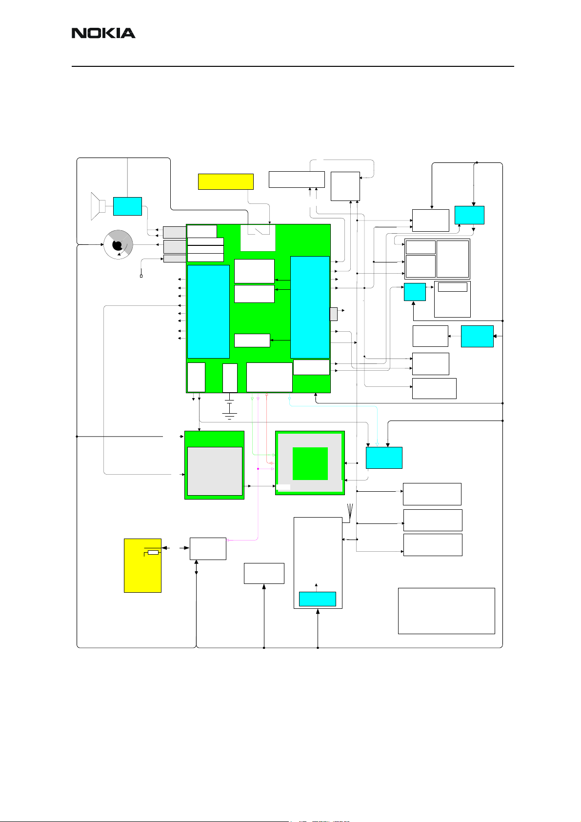
Power Distribution
The connection of the miscellaneous power connection can be seen in the following
overview.
Figure 1: Power distribution
VBUS
VCC
ACI
VOUT
VAUX3
VANA2.78V
VFLASH1
VSIM
VAUX1
VCORE1.0-1.8V
1,8V VIO
DLight
KLight
NUT
ESD
Display
illumination
LCD Driver
LED
driver
IR
Module
Memory
Card
CCP
Camera
FM Radio
Parallel
Display
Keyb Light
Keyboard
2.8V
LED
driver
LP3987
HF
Speaker
Vibra
Amplifier
"On Key"
CHARGER
PAOUTN
ESD
PAOUTP
Vibra
ESD
BuzzO
PwrOnX
ESD
VR1A 4.75V
VR1B 4.75V
VR2
2.78V
2.78V / 3.6V
VR3
2.78V / 3.6V
VR4
2.78V / 3.6V
VR5
2.78V / 3.6V
VR6
2.78V / 3.6V
VR7
RF Regulators BB Regulators
VRefRF02
VRefRF01
VBack
VCharOut
BTEMP
RF CODECS
AUDIO CODEC
DIGITAL
BLOCKS
DIGITAL
BLOCKS
VBack
LS
BSI
PURX
SleepClk
SleepX
TOMAHAWK
VCharIn
UEMRstX
UEME
2.78V VAUX2
2.78V
2.78V
1.8/3.0V
1.8/3.0V
1.8V
Lynx
Battery
VBAT_RF
VXO
BATT
BSI
RF
ZOCUS-C
HELGA
EDGE
RFClock
BC02
TIKU
1.5V
VCORE
LM2708
SDRAM 64Mb
FLASH 64Mb
FLASH 64Mb
FCI
VBAT
2.8V
MAS9161
Matrix
Power Distribution Diagram
Ver. 0.3 Søren Larsen, Copenhagen
15.05.2003
CONFIDENTIAL
Copyright 2002 Nokia Mobile Phones
Issue 1 02/04 Nokia Corporation Page 15
Page 16

RH-12/RH-28
System Module CCS Technical Documentation
Tiku
This is the main digital baseband ASIC.
Main Features
The Tiku consists of the following sections:
• Arm 925 MPU
• A-DSP (Lead3 for Application sw – 4KB ApiRam, 128KB saram, 32KB daram)
• C-DSP (Lead3 for Cellular sw – 4KB ApiRam, 128KB saram, 32KB daram)
• DSP Co-processors (DCT and Motion Estimator) on both DSP
• Corona EDGE hardware accelerator
• Serial flash interface (SFI001)
• 2G Body logic, as in UPP-WD2
• 4Mb of pdram.
• Traffic controller for memory interface (dct4 flash/sram, sdram)
• General purpose USARTs
• SIM card interface
•2nd SIM interface (used for MMC)
2
C interface (used for FCI)
•I
• GSM coder
• Interface control for: keyboard, LCD, Camera, audio and UEME control
• Accessory interfaces: IrDa and LPRF (Bluetooth)
• Handling of RF-BB interface
• I/O voltage = 1.8V, Core voltage = 1.5V
• TI 15C035 process (Tiku version 1.11)
• 288 pins uBGA, 0.5mm pitch, 12 mm x 12 mm package (Tiku version 1.11)
The Brain consists of 5 sections; the ARM925 Mega-Module, (consisting of the ARM9
Page 16 Nokia Corporation Issue 1 02/04
Page 17

RH-12/RH-28
CCS Technical Documentation System Module
MCU, Cache memory, Parallel LCD Controller, and Traffic Controller), C-DSP Lead 3
Mega-Module, A-DSP Lead 3 Mega-Module, PDRAM, and PDA Peripherals.
The ARM-Mega-Module has a Traffic controller, which provides the interface between
the MCU, external memories, LCD controller, and internal busses. It also processes the
data packages for memory access.
The PDA Peripherals consists of Camera Compact Port (CCP) interface, Multi-Media Card
(MMC), IR, USB, and Display interfaces.
Memory Block
For the MCU, TIKU includes ROM, 2 kbytes, that is used mainly for boot code of MCU.
For the program memory, 4Mbit (256K x 16bit, organized as 8 banks of 64Kb) PDRAM is
integrated. RAM is mainly for MCU purposes. The MCU can also store a code into the
external flash memory, which consist of one NOR flash and one NAND flash. The size of
the NOR flash is 128Mbit (8Mbit x16bit) and it’s used for primary application code. The
secondary flash is a NAND flash, which is used for slow accessible data such as user-settings, pictures, ringtones etc. (non speed dependent code). The size of the NAND flash is
64Mbit (4096K x 16 bit).
Memory
The external memory interface consists of three different type of memory, used for different purposes.
NOR Flash
The NOR flash is used as the primary data storage. Here the MCU sw package is stored.
Furthermore, the memory is capable of handling burst mode (multiplexed address/databus) and memory blocking, which is controlled by TIKU.
NAND Flash
The NAND flash is used as the secondary data storage, mainly used for user specific data
like sounds, games, pictures and other applications. This device also stores language
package.
SDRAM
The SDRAM is used as a data handling memory.
The SDRAM interface to TIKU is different than the 24 lines multiplexed data/address bus
used for the flash memory. First the address is set up then the data is latched out in a
normal asynchronous/synchronous way. In the synchronous mode, the data is clocked
out at a maximum frequency at 133MHz.
Issue 1 02/04 Nokia Corporation Page 17
Page 18

RH-12/RH-28
System Module CCS Technical Documentation
Charging
The RH-12/RH-28 program is conform to the global NMP Charger Interface.
This comprehensive interface ensures future proofing should new chargers become available.
Charging is controlled by the UEME and external components are needed for EMC,
reverse polarity and transient protection of the input to the baseband module. The
charger connection is through the system connector interface. The DCT4.5 baseband is
designed to support DCT3 chargers from an electrical point of view. Both 2- and 3-wire
type chargers are supported. 3-wire chargers are treated as 2-wire (PopPortTM specifications).
The operation of the charging circuit has been specified in such a way as to limit the
power dissipation across the charge switch and to ensure safe operation in all modes.
Figure 2: Charging
CHARGER
Filter
cap.
VBATBB
TRANSCEIVER
10nF
1uF
0R22
VCHAROUT
VBATREGS
Charger
CHACON
UEME
Section
VCHARIN
Feedthrough cap
27pF
SMF16A
GNDGNDGND
GND
GND
1,5A
1uF
GND
Connecting a charger creates voltage on VCHAR input. When VCHAR input’s voltage
level is detected to rise above the VCHDET+ threshold by CHACON, the charging starts.
The VCHARDET signal is generated to indicate the presence of the charger. However,
detection output signal must be gated always to a logical ‘0’ when MSTRX=‘0’, in order
not to force logical high level to the UEME’s internal blocks that are not supplied at the
time. Level crossing detection of the VCHAR line is used to generate synchronizing pulses
for UEME’s state machine for control of rectifier type chargers. The VCHARDET output
gives a logical ‘1’ when the VCHAR input is detected to be above the VCHDET+ level and
‘0’ when the VCHAR input level is below VCHDET.
Figure 3: Detection of charger / generation of charger synchronisation pulses
GND
1000uF
max
Page 18 Nokia Corporation Issue 1 02/04
Page 19

RH-12/RH-28
CCS Technical Documentation System Module
In case the main battery is fully discharged and the UEME subsequently is without
power, i.e. in NO_SUPPLY or BACKUP mode, the start-up charging circuitry is in control,
giving the possibility to detect a charger and engage charging. If the VBAT level is
detected to be lower than the master reset voltage (VMSTR-) the CHACON will charge
the battery with a constant current of 100 mA until VBAT exceeds VMSTR+. When this
happens, from a charging point of view, normal PWM charging situation resumes. A
PWM signal is generated by the digital part of the UEME, which sources the CHACON.
The frequency of the signal can be either 1 Hz or 32 Hz. If the connected charger is of a
2-wire kind, e.g. ACP- 7, the PWM signal has the frequency of 1 Hz. If the charger on the
other hand is a 3-wire type, e.g. ACP-9, the switch is left on permanently and the 32 Hz
PWM control signal routed to the charger in order to produce a constant voltage.
Issue 1 02/04 Nokia Corporation Page 19
Page 20

RH-12/RH-28
System Module CCS Technical Documentation
Battery
Type: BL-5C
Technology: Li-Ion. 4.2V charging. 3.1V cut-off
Capacity: 850 mA/h (BSI=75K)
The battery is a Li Ion based standard cell with LiMnO chemistry.
This type of battery has a three-pin connector (BTEMP is not used).
Figure 4: BL-5C Battery
Table 3: BSI Levels BL-5C Battery
Mode BSI (kOhm / Description
Min Type Max
Normal 75 Used for calculating the Capacity (BL5-C = 850mA)
Service 3.2 3.3 3.4 Pull-down resistor in battery. Used for fast power-up in pro-
duction (LOCAL mode), R/D purposes or in aftersales, 1% tolerance resistors shall be used.
Test 6.7 6.8 6.9 Pull-down resistor in battery, used in production for testing
purposes. 1% tolerance resistors shall be used.
Banned <3.2
Inside the battery, an over-temperature and an over-voltage protection circuit are implemented.
Care should be taken with the temperature. If the battery is charged above 60 degrees
Celsius, overheating might occur.
Interfaces
FM-Radio
The FM radio circuitry is implemented using a highly integrated radio IC, TEA5767HN.
The MCU SW controls the FM radio circuitry through serial bus interface.
The stereo output is fed to the UEME on one of the microphone inputs.
Page 20 Nokia Corporation Issue 1 02/04
Page 21

RH-12/RH-28
CCS Technical Documentation System Module
The antenna of the FM Radio is created with the headset. The wires of the headset are
used as poles of the antenna.
Only version TEA5767HN-VF1 and newer can be used. The previous versions have a 2.78V
digital interface and need level shifters.
While W/R (WRITE/READ) is HIGH the TIKU can transmit data to the TEA5767. At the rising edge of the Bus clock, the register shifts and accepts the stable bit. At clock low the
TIKU writes the following bit. A tuning function is started when the W/R signal changes
from HIGH to LOW. Was a search tuning requested sent, the IC autonomously starts
searching the FM band. Search direction and search stop level can be chosen. Was a station with a fieldstrength equal or higher than this stop level found, the tuning system
stops and the Found Flag bit is set to “HIGH”. Was during search a band limit reached,
the tuning system stops at the band limit and the Band Limit flag bit is set to high. Also
the Found Flag is set to high in this case.
While Write/Read is “LOW” the Tiku EDGE can read data. At the rising edge of the BUS
Clock, data will be shifted out of the register. This data is available from the point where
the bus clock is HIGH until the next rising edge of the clock occurs.
Interface to Engine
GENIO8
GPIO22
GPIO24
GPIO25
FMCtrlDa
FMCtrlClk
FMWrEn
FMClk
VIO
GND
Figure 5: FM Radio schematic
TEA5767
SDA
SCL
W/R
Clk
VAFL
VAFR
Ant
VDIG
GND
UEMETIKU
Filter
L1
VFLASH1
1U
MIC3NR
MIC3PR
MIC3N
MIC3P
C1
C2
C3
C4
1
14
Tomahawk
IrDA
The RH-12/RH-28 phone supports data connectivity via the Infra Red link. The IR interface is integrated into the TIKU and the main external component is the IR module. The
datarate supported will be 1.152Mbit.
Issue 1 02/04 Nokia Corporation Page 21
Page 22

RH-12/RH-28
System Module CCS Technical Documentation
Interface to Engine
This interface receives data from and transmits data to peripheral equipment. It transforms serial data to parallel data for the MCU or DSP and vice versa. The IAccIF IR interface is divided into two blocks, MIR and FIR. IR is a UART-based block for baud rates in
the range 9600 bit/s to 115.2 kbit/s, and FIR is for the 1.152 Mbit/s rate. Both parts have
the same physical connections so they cannot be used simultaneously. The shut down pin
SD can power off the module.
The maximum distance in the RH-12/RH-28 phone configuration is approximately 20
centimetres.
The SIR block (9600 bit/s to 115.2 kbit/s):
• Supports IrDA format with speeds up to 115.2 kbit/s
• Supports Phonet format, having all the same baud rates (9600 bit/s – 115.2kbit/s)
as Fbus.
The FIR block (1.152 Mbit/s):
• Supports IrDA format with baud rate 1.152 Mbit/s.
• Both these blocks are sub-divided into IR transmitter and IR receiver. Interconnection details are shown in the following figure and table.
Figure 6: IRDA Interconnections between Tiku and UEME
UEME
VIO
VFLASH1
Tiku EDGE
IRSD(GenIO23)
IrRx (GPIO 0)
IrTx (GPIO 1)
VBATT
IR Module
LEDA
V
LOGIC
Vdd
LEDC
GND
SD
RxD
TxD
Table 4: IRDA connections between Tiku EDGE and the IR module
Name I/O Engine connection Description
TXD O TIKU GPIO1: [IRTx] Transmitted data output to IR Module
RXD I TIKU GPIO0: [IRRx] Received data input from IR Module.
Page 22 Nokia Corporation Issue 1 02/04
Page 23

RH-12/RH-28
CCS Technical Documentation System Module
SD O TIKU GenIO23: [IRSD] IR Module shut down.
VLOGIC O UEME VIO Supply voltage for digital parts, 1.8 V.
VCC O UEME VFLASH1 IR Module supply voltage, 2.78 V.
LEDA O VBATT IR LED Anode supply voltage.
Camera
The RH-12/RH-28 phone is equipped with a VGA resolution camera with an active area
of 660H x 492V. Pictures delivered to engine are standard VGA (640 x 480). This camera
is able to transfer up to 30 frames per second in the viewfinder mode and 15 frames per
second in full resolution mode (VGA). Full resolution pictures are in RGB 5:6:5 or YUV
4:2:2 (10 bits raw sensor resolution). The camera used is a Mirage-1 TCM8100MD module.
Mounting
The camera is placed physically almost inside the antenna on the backside of the phone
PWB. The camera fixture (spring type, see the figure below) is located between the RF
shielding cans. Shielding is done in a combination of metalized plastic housing of the
camera module and ground connected spring/clip fixture.
Experience shows that good shielding is necessary. The metalized housing and the spring/
clip will shield the camera. The hole for the lens is kept as small as possible to avoid
direct EMC entrance into camera module by lens opening.
Interface to Engine
The camera is connected to the TIKU via a dedicated differential camera bus called CCP.
The control of the camera is routed through normal-type general I/O ports. The camera
uses 2 different supplies; analog and digital supply.
Spring/clip fixture
Figure 7: Camera Module Mounting
Lens
Camera module
(metalized plastic)
Camera connector
CMOS
sensor
Springs
PWB
Issue 1 02/04 Nokia Corporation Page 23
Page 24

RH-12/RH-28
System Module CCS Technical Documentation
Figure 8: Camera Interface
Camera TIKU
100R
100R
4k7
C1
CIFDaP
E4
CIFDaN
D2
CIFClkP
F4
CIFClkN
L
GenIO26 (SDA (I2C) CAM)
4
L
GenIO25 (SCI (I2C) CAM)
7
K3
GenIO24 CAMClk)
L
GenIO27 CAMVCtrl)
3
CCPDATAP
CCPDATAN
CCPCLKP
CCPCLKN
SDA
SCL
EXTCLK
XSHUTDOWN
1
3
1
2
1
0
9
7
6
5
4
VIO
CCP(0)
CCP(1)
CCP(2)
CCP(3)
4k74k7
3p3
1
DGND
VDIG
DGND
VANA
AGND
SHIELD
4
1
1
8
3
2
100n 100n
1
600R/100MHz
600/100MHz
1
VCORE
3
1
VFLASH1
3
27p27p
Power supply to the camera module doesn't need to be shut down when the camera is in
the idle mode. The camera uses very low stand-by current (1 mA in current spec).
UEME
Page 24 Nokia Corporation Issue 1 02/04
Page 25

RH-12/RH-28
CCS Technical Documentation System Module
SIM
The UEME contains the SIM interface logic level shifting. The SIM interface can be programmed to support 3V and 1.8V SIMs.
The SIM interface is powered up when the SIMCardDet signal indicates, ”card in”. This
signal is derived from the BSI signal.
Interface to Engine
Figure 9: TIKU/UEME SIM Interface Connections
SIM
C5C6C7
C1C2C3
C8
C4
From Battery
type contact
UEME
SIMIF Block
SIMData
SIMClk
SIMRst
VSIM
BSI
GND GND
Data
SIMClk
SIMIO
UEME Dig.
Logic
Tiku
Data
SIMClk
SIMIO
UIF Block
UEMInt
CBusDa
CBusEnX
CBusClk
The internal clock frequency from the CTSI Block is 13 MHz in GSM.
Issue 1 02/04 Nokia Corporation Page 25
Page 26

RH-12/RH-28
System Module CCS Technical Documentation
Figure 10: SIM Interface Data
MMC
The RH-12/RH-28 phone is equipped with a standard MMC card connector. The MMC
card is physically placed under the battery, on top of the BB shielding can. The MMC card
can be replaced when the phone is powered off, and the b-cover and battery are
removed. The RH-12/RH-28 phone is able to accept all known high and dual voltage
types of MMC cards. Only limitation is a maximum current withdrawal of 150 mA, where
the maximum current class of MMC cards is 200mA.
Table 5: VMMC power specifications
Name Voltage (V) Current (mA) Filter Comment
Min Nom Max Max
VMMC 2.76 2.85 2.94 150 1
Page 26 Nokia Corporation Issue 1 02/04
Page 27

RH-12/RH-28
CCS Technical Documentation System Module
Mounting
The MMC card is mounted as shown in the figure below, seen from the backside of the
phone, with the b-cover and battery removed. The MMC card slides in from the right
side.
Figure 11: MMC Card Placement
Interface to Engine
The MMC card is connected to the engine at UEME. MMC uses the dedicated MMC/secondary SIM (SWIM) card interface.
As it can be seen in the figure below, the MMC card uses an external regulator VMMC
as supply.
Tiku EDGE
GPIO15
GPIO17
GPIO19
GPIO16
GPIO18
Figure 12: MMC Card Engine Interface
UEME
GEN18i01
GEN18i02
GEN18i03
GEN18i04
GEN18i05
GENIO28i01
GENIO28i02
GENIO28i03
Level shifters
LDO
Voltage
regulator
2,85V
MMC Clock
MMC Cmd
MMC Data
MMC Card
Bluetooth
The Bluetooth solution for the RH-12/RH-28 phone is a single chip solution designed by
CSR.
Issue 1 02/04 Nokia Corporation Page 27
Page 28

RH-12/RH-28
System Module CCS Technical Documentation
Interface to Engine
Figure 13: BT HW Interface
Vbatt (3 - 5,4V)
2,8V LDO
PURX
ENABLE
BB 4.5
Power Management
The external BT regulator is enabled by PURX, witch is an internal UEME reset signal. This
signal is high whenever the phone is powered on, which also is the case in sleep.
This means that the BC02 module power is always on. Due to this, the modules use sw
power down, witch results in a constant current consumption of approx. 100µA, when
the BC02 module is in sleep.
VIO
RF_Clock
PCM_CLK
PCM_IN
PCM_OUT
PCM_SYNC
BT_ResetX
UART_RX
UART_TX
UART_RTS
UART_CTS
BT_WAKEUP
HOST_WAKEUP
VDD_IO
XTAL_IN
PCM_CLK
PCM_OUT
PCM_IN
PCM_SYNC
RESETX
UART_TX
UART_RX
UART_CTS
UART_RTS_P - PIO(2)
UART_CTS_P - PIO(3)
BT_WAKEUP - PIO(4)
HOST_WAKEUP - PIO(6)
VREG_IN
BC02
1,8V
LDO
VDD_ANA
VDD_RADIO
VDD_VCO
VDD_CORE
VDD_MEM
FLASH_EN
TX_A
TX_B
RF Filter +
Balun
Sw Interface
Host and Bluetooth module interface can be logically divided into audio, user data and
control interfaces.
User audio at 8 ksamples/s is exchanged between the host and the Bluetooth module on
a PCM connection. (Optionally, the audio data can be multiplexed on a logical UART
channel).
Accessorey Interface (ACI)
ACI (Accessory Control Interface) is a point-to-point, Master-Slave, bi-directional serial
bus. ACI supports the following features:
• The identification of accessory type is provided
• The insertion and removal detection of an accessory device
Page 28 Nokia Corporation Issue 1 02/04
Page 29

RH-12/RH-28
CCS Technical Documentation System Module
• Providing power to the accessory: 200mW Power out
• Reference voltage to the accessory
The insertion / removal detection is provided by the HeadInt input.
Figure 14: ACI schematics
Phone Board
Tomahawk
ACI Accessory
Cbypass
GND
Ccom
56K
GND
GND
ACI ASIC
Authentication
Comm.
Logic
RC
Clock
EEPROM
I/O
Logic
GND
TIKU
ARM
IRQ
FIQ
CBUS
PUP
ACI Block RX
UEME
HeadInt
Comp.
TX
Level
Shifter
Vhead
VAUX2
Vflash1
VFLASH1
HEADINT
VOUT
120k
ACI
GND
GND
The Vout pin on the PopPortTM provides external power to accessories. The Vout is supplied by VAUX2 and can be controlled by the UEME. VAUX2 is short circuit protected.
Table 6: Vout specifications
Voltage (V) Current (mA)
Name
Min Nom Max Max
Sleep
Max
VAUX2 2.70 2.78 2.86 70 0.5 1
FBUS
More intelligent accessories can use the serial FBUS connection.
These devices can use Vout as the power supply and ACI for identification.
FBUS is an asynchronous data bus having separate TX and RX signals. Default bit rate of
the bus is 115.2 Kbit/s. FBUS is mainly used for controlling the phone in the production
and for interface to PC via serial cables. Tiku can also support fast bus. This is FBUS with
a bitrate of 1.2Mbit.
Filter Comment
Issue 1 02/04 Nokia Corporation Page 29
Page 30

RH-12/RH-28
System Module CCS Technical Documentation
Fbus is using the same pins as the USB connection.
Table 7: Fbus signals
Voltage (V)
Name Name
Min Nom Max
FBUS RX VIH 1.95 2.78 3.00 0.7*VFLASH1
VIL 0 0.20 0.83 0.3*VFLASH1
FBUS TX VOH 1.95 2.78 3.00 0.7*VFLASH1
VOL 0 0.20 0.83 0.3*VFLASH1
Rise Time 12.5ns For Rx and Tx signals
Comment
USB
The Nokia USB device solution is supported using the Wireless 2 Function Controller
(W2FC) core. This core is included in the TIKU ASIC. The core completes several USB functions automatically and is controlled by the ARM9 MCU.
NUT provides the interface between the ASIC's 1.8 V bus and the 3.3 V USB bus. In addition, NUT is capable of transmitting and receiving Fbus signals to and from the Fbus
UART in Tiku.
Nokia USB Transceiver (NUT) is fully compliant with the Universal Serial Bus Specification Rev. 1.1.
NUT is able to transmit and receive serial data at full-speed (12 Mbit/s).
The USB signal ESD protection and line matching resistance, and USB pull-up resistor is
included to the USB ASIP. This component also includes ESD protection for VOUT and ACI
system connector pins.
Page 30 Nokia Corporation Issue 1 02/04
Page 31

RH-12/RH-28
CCS Technical Documentation System Module
Figure 15: USB Circuit
UI Interface
Display Unit
Hardware Interface:
The Display Unit interface is a parallel interface consisting of the following:
A 24-pin connector as shown in the figure below provides the interface between the Display Unit and the Engine PWB.
Internally, the TIKU DIF block has interfaces with the VIA bus and the secondary DMA
controller.
Interconnection details are shown in the figure below.
• 8-bit data bus (DISPDATA(7:0))
• Write enable WRX
• Read enable RDX
Issue 1 02/04 Nokia Corporation Page 31
Page 32

RH-12/RH-28
System Module CCS Technical Documentation
Figure 16: Display Unit Connections
Tiku
UEME
LED Drivers
DIFDa[7:0]
Display Unit
WRX
RDX
A0
TE
RESETX
VIO
VFLASH1
P_S
VLED1+
VLED2+
VLED3+
VLED-
CSX
GND
GND
GND
GND
Keyboard and Navigator
The RH-12/RH-28 phone consists of a mainboard with interface to the UI board. The
connection between the main board and the UI board is via a board-to-board connector.
The signals on the board-to-board connector are:
• Signals for LED's
• Signals for numeric Keypad and navigation key
The UI board is the base for the keyboard, which includes a five-way navigation key.
Page 32 Nokia Corporation Issue 1 02/04
Page 33

RH-12/RH-28
CCS Technical Documentation System Module
Figure 17: Keyboard layout with special keys for Navi_Up, Navi_Down and Navi_Select
Issue 1 02/04 Nokia Corporation Page 33
Page 34

RH-12/RH-28
System Module CCS Technical Documentation
Table 8: Keyboard allocation Tiku GPIO
Keypad matrix and
Navigation key
Navigation
Key
Keypad Column 0 Tiku GPIO 2 Tiku, Keyboard interface KDI in the UIF block,
Left Tiku - Separate controllines (Special keys) for
Up GPIO 6
Right -
Down GPIO 7
Select GPIO 13
GND -
Column 1 GPIO 3
Column 2 GPIO 4
Column 3 GPIO 5
Row 0 GPIO 8
Row 1 GPIO 9
Row 2 GPIO 10
Tiku connection Description
Navi_Up, Navi_Down and Navi_Select.
Navi_Left and Navi_Right are connected to the
keyboard matrix
Multiple-keypress:
The RH-12/RH-28 phone will implement multiple keypress. By multiple keypress we
mean the ability to detect that the user has pressed several keys simultaneously. The
incitement for implementing this functionality is mainly the support for Java and the
requirements set by games.
UI software is capable of supporting multiple keypress, while core SW will have to incorporate this feature into the keyboard driver.
With the current implementation, the design supports 2 simultaneously arbitrarily
pressed keys in the keyboard matrix, together with any combination of Navi_Up,
Navi_Select and Navi_Down (The special keys).
LED Driver
The RH-12/RH-28 phone UI module has 2 sets of LED's:
Row 3 GPIO 11
Row 4 GPIO 12
• 3 pcs. for LCD – LED: White
• 2 pcs. for Keyboard (prepared for 4) – LED: White, sidefiring
Both groups are individual controllable by the PWM output signal from UEME ASICs
Page 34 Nokia Corporation Issue 1 02/04
Page 35

RH-12/RH-28
CCS Technical Documentation System Module
Figure 18: . LED driver block
Vbat
Vibra
Dlight
UEME
TK11851L
LCD
Keypad
configuration
is optional
Intensity Control:
LEDs are controlled by the PWM output from UEME UI block. The PWM controls can be
adjusted in 8-bit step (256). The TK11851L contains a sleep mode. This mode is achieved
when the Dlight signal is low.
A vibra-alerting device is used to generate a vibration signal for an incoming call. The
vibra is placed in the top of the phone. It is placed in the D-cover next to the microphone.
The vibra is electrically connected to the PWB by spring contacts.
The vibra is controlled from the UEME by a PWM (Pulse Wide Modulated) square wave
signal.
IHF-speaker
Alerting tones and/or melodies are generated by an Internal HandsFree speaker, which is
controlled by a PWM signal from the UEME.
The ringer melodies will be optimised in MCU so the main frequency of any given melody
is shifted to near the resonant peak. Sound hole is placed in the D-cover The IHF is electrically connected to the PWB by spring contacts.
Issue 1 02/04 Nokia Corporation Page 35
Page 36

RH-12/RH-28
System Module CCS Technical Documentation
RF Interface
The interface between baseband and the RF section is shown below:
Figure 19: Simplified RF/BB Interface Block Diagram
RF_BB interface
Antenna Switch
RF_RF interface
VCO
RF
BB
Zocus-C
Edge Mode
Battery
BL-5C
PA LNA
LNA2, Mixer,
AGC, DTOS
Tx IQ modulator
IPA1
IPA2
TxPwrDet
TXC
7xVreg
RFtemp
UEME
RFI and Codec
BB & RF regulators
TxI/QDa
2
RFConvClk
MCU, ASIC, CDSP & ADSP
4 GHz
PLL, Dividers
HELGA
26 MHz
26 MHz
TXA
Reset
LPRF Clk 26 MHz
TXP
2xVref
Tx I/Q
Rx I/Q
2
4
VCTCXO
AFC
BC 02
BT Module
AuxD
RxI/QDa
2
DBUS
3
RF-Bus: Ena, Clk & Data
TIKU
Test Pattern
Test pads are placed on engine PWB for service.
RH-12/RH-28 has adopted the two-row test pattern layout. The basic test pads
(FBUS_TX, FBUS_RX, VPP, MBUS & GND) have a defined location, while optional signals
can be on either side of the test pads. The ‘DAI_CLK’ is included as an optional signal.
For specific test pad placement, please see the figure below.
Page 36 Nokia Corporation Issue 1 02/04
Page 37

RH-12/RH-28
CCS Technical Documentation System Module
Figure 20: Production Test Pattern
1: TXD / FBUS_Tx
2: RXD / FBUS_Rx
1 2 3
4 5 6
3: DAI_CLK
4: VPP
5: SCK / MBUS
6: GND
Issue 1 02/04 Nokia Corporation Page 37
Page 38

RH-12/RH-28
System Module CCS Technical Documentation
Test Points
See the following two figures for an indication as to where some of the test points can
be found.
Main board A side of PWB
STJRxD
GENTEST0/STJTxD
J471
VBAT
J473
J470
SDRCKE
J402
SDRAd0
SDRDa0
J416
J417
GENTEST1/STJClk
EMU1
EMU0
J488
J487
JTD0
J483
JClk_rst
J484
JTRst
J485
J481
J489
GND
J482
JTDI
VCC
JTMS
J480
JTClk
J486
J472
J474
GND
DBusClk
DBusEn1X
J410
J407
SleepX
J403
DBusDa
MMICS0X
J420
MMIDa0
CBusEnX
CBusClk
J412
CBusDa
J413
UEMInt
PURX
J408
J404
J411
J414
SleepClk
J401
J418
Page 38 Nokia Corporation Issue 1 02/04
Page 39

RH-12/RH-28
CCS Technical Documentation System Module
Main board B side of PWB
J306
IHF1
J307
IHF0
VBAT
J100
J101
BSI
FMCtrlDa
FMWrEn
USBRxP
J110
USB6Z
USBRx
J108
USBRxM
J107
J109
Vpu
USBSuspend
J113
J104
D+/RXD
D-/TXD
USBTx
USBSE
J111
J112
J106
J105
FCI Int
J318
FCI sda
FCI scl
J317
J316
J356
J358
FMCtrlClk
FMClk
J359
J357
FCI supply
J315
J319
GND
Issue 1 02/04 Nokia Corporation Page 39
Page 40

RH-12/RH-28
System Module CCS Technical Documentation
RF Module Introduction
The RF module performs the necessary high frequency operations of the EGSM900/
GSM1800/GSM1900 triple band (EDGE) engine in the RH-12/RH-28 product. The
EGSM900 is rematched to GSM850 in the RH-28 product.
Both, the transmitter and receiver have been implemented by using direct conversion
architecture, which means that the modulator and demodulator operate at the channel
frequency.
The core of the RF is an application-specific integrated circuit, Helgo. Another core component is a power amplifier module, which includes two amplifier chains, one for
GSM850/EGSM900 and the other for GSM1800/GSM1900.
Other key components include:
• 26 MHz VCTCXO for frequency reference
• 3296-3980 MHz SHF VCO (super high frequency voltage controlled oscillator)
• front end module comprising a RX/TX switch and two RF bandpass SAW filters
• three additional SAW filters
The control information for the RF is coming from the baseband section of the engine
through a serial bus, referred later on as RFBus. This serial bus is used to pass the information about the frequency band, mode of operation, and synthesizer channel for the RF.
In addition, exact timing information and receiver gain settings are transferred through
the RFBus. Physically, the bus is located between the baseband ASIC called UPP and
Helgo. Using the information obtained from UPP, Helgo controls itself to the required
mode of operation and further sends control signals to the front end and power amplifier
modules. In addition to the RFBus, there are still other interface signals for the power
control loop and VCTCXO control and for the modulated waveforms.
The RF circuitry is located on the top side of the 8 layer PWB.
EMC leakage is prevented by using a metal cans. The RF circuits are separated to three
blocks:
•FM radio
• PA, front end module, LNA and 1900 band SAWs
• Helgo RF IC, VCO, VCTCXO, baluns and balanced filters
The RF transmission lines constitute of striplines and microstriplines after PA.
The baseband circuitry is located on the one side of the board, which is shielded with a
Page 40 Nokia Corporation Issue 1 02/04
Page 41

RH-12/RH-28
CCS Technical Documentation System Module
meallized frame and ground plane of the UI-board.
RF Frequency Plan
RF frequency plan is shown below. The VCO operates at the channel frequency multiplied
by two or four, depending on the frequency band of operation. This means that the baseband-modulated signals are directly converted up to the transmission frequency and the
received RF signals directly down to the baseband frequency.
Figure 21: RF Frequency Plan
DC Characteristics
Regulators
The transceiver baseband section has a multi-function analog ASIC, UEM, which contains
among other functions six pieces of 2.78 V linear regulators and a 4.8 V switching regulator.
All regulators can be controlled individually by the 2.78 V logic directly or through a control register.
The use of the regulators can be seen in the power distribution diagram, which is presented in the Figure Power Distribution Diagram below.
Issue 1 02/04 Nokia Corporation Page 41
Page 42

RH-12/RH-28
System Module CCS Technical Documentation
The seven regulators are named VR1 to VR7. VrefRF01 and VrefRF02 are used as the reference voltages for the Helgo, VrefRF01 (1.35V) for the bias reference and VrefRF02
(1.35V) for the RX ADC (analog-to-digital converter) reference.
The regulators (except for VR7) are connected to the Helgo. Different modes of operation
can be selected inside the Helgo according to the control information coming through
the RFBus.
Table 9: List of the needed supply voltages
Volt. Source Load
VR1 PLL charge pump (4.8 V)
VR2 TX modulators, VPECTRL3s (ALC), driver
VR3 VCTCXO, synthesizer digital parts
VR4 Helgo pre-amps, mixers, DtoS
VR5 dividers, LO-buffers, prescaler
VR6 LNAs, Helgo baseband (Vdd_bb)
VR7 VCO
VrefRF01 ref. Voltage for Helgo
VrefRF02 ref. Voltage for Helgo
Vbatt PA
Typical Current Consumption
The table below shows the typical current consumption in different operation modes.
Table 10: Typical current consumption in different operation modes
Operation mode Current consumption Notes
Power OFF < 10 uA Leakage current (triple band PA)
RX, EGSM900 75 mA, peak
RX, GSM1800/GSM1900 70 mA, peak
TX, power level 5, EGSM900 1700 mA, peak
TX, power level 0, GSM1800/
GSM1900
1000 mA, peak
Page 42 Nokia Corporation Issue 1 02/04
Page 43

RH-12/RH-28
CCS Technical Documentation System Module
Power Distribution
Figure 22: Power Distribution Diagram
RF Characteristics
Table 11: Channel Numbers and Frequencies
System Channel number TX frequency RX frequency Unit
GSM850 128 <= n <= 251 F = 824.2 + 0.2∗(n – 128) F = 869.2 + 0.2∗(n-128) MHz
GSM900 0 < =n <=124 F = 890 + 0.2∗n F = 935 + 0.2∗n MHz
975<= n <= 1023 F = 890 + 0.2∗ (n -1024) F = 935 + 0.2∗(n -1024) MHz
GSM1800 512 <= n <= 885 F = 1710.2 + 0.2∗ (n-512) F = 1805.2 + 0.2∗ (n-512) MHz
GSM1900 512 <= n <=810 F = 1850.2 + 0.2∗ (n-512) F = 1930.2 + 0.2∗ (n-512) MHz
Issue 1 02/04 Nokia Corporation Page 43
Page 44

RH-12/RH-28
System Module CCS Technical Documentation
Table 12: Main RF Characteristics
Parameter Unit and value
Cellular system[RH-12]
[RH-28]
RX Frequency range GSM850: 869 … 894 MHz
TX Frequency range GSM850: 824 … 849 MHz
Duplex spacing GSM850: 45 MHz
Channel spacing 200 kHz
Number of RF channels GSM850: 124
Output Power GSM850: GSMK 5…33 dBm
EGSM900/GSM1800/GSM1900
GSM850/GSM1800/GSM1900
EGSM900: 925 ... 960 MHz
GSM1800: 1805...1880 MHz
GSM1900: 1930...1990 MHz
EGSM900: 880 ... 915 MHz
GSM1800: 1710 ...1785 MHz
GSM1900: 1850 …1910 MHz
EGSM900: 45 MHz
GSM1800: 95 MHz
GSM1900: 80 MHz
EGSM900: 174
GSM1800: 374
GSM1900: 300
GSM850: 8-PSK 5…27 dBm
EGSM900: GSMK 5…33 dBm
EGSM900: 8-PSK 5…27 dBm
GSM1800: GSMK 0…30 dBm
GSM1800: 8-PSK 0…26 dBm
GSM1900: GSMK 0…30 dBm
GSM1900: 8-PSK 0…26 dBm
Number of power levels GMSK GSM850: 15
EGSM900: 15
GSM1800: 16
GSM1900: 16
Number of power levels 8-PSK GSM850: 12
EGSM900: 12
GSM1800: 14
GSM1900: 14
Page 44 Nokia Corporation Issue 1 02/04
Page 45

RH-12/RH-28
CCS Technical Documentation System Module
Table 13: Transmitter Characteristics
Item Values (EGSM900/1800/1900)
Type Direct conversion, nonlinear, FDMA/TDMA
LO frequency range GSM850: 3296…3395 MHz (4 x TX freq)
EGSM900: 3520...3660 MHz (4 x TX freq)
GSM1800: 3420...3570 MHz (2 x TX freq)
GSM1900: 3700...3820 MHz (2 x TX freq)
Output power
(GSM850/EGSM900/GSM1800/GSM1900)
Table 14: Receiver Characteristics
Item Values, EGSM900/1800/1900
Type Direct conversion, Linear, FDMA/TDMA
LO frequencies GSM850: 3476…3575 MHz (4 x RX freq)
Typical 3 dB bandwidth +/- 91 kHz
Sensitivity min. - 102 dBm (normal condition)
Total typical receiver voltage gain (from antenna to RX
ADC)
Receiver output level (RF level -95 dBm) 230 mVpp, single-ended I/Q signals to RX ADCs
GMSK 33/33/30/30 dBm
8-PSK 27/27/26/26 dBm
EGSM900: 3700...3840 MHz (4 x RX freq)
GSM1800: 3610...3760 MHz (2 x RX freq)
GSM1900: 3860...3980 MHz (2 x RX freq)
86 dB
Issue 1 02/04 Nokia Corporation Page 45
Page 46

RH-12/RH-28
System Module CCS Technical Documentation
RF Block Diagram
The block diagram of the RF module can be seen in the following figure. The detailed
functional description is given in the following sections.
Figure 23: RF Block Diagram
HELGO
Page 46 Nokia Corporation Issue 1 02/04
Page 47

RH-12/RH-28
CCS Technical Documentation System Module
Frequency Synthesizers
The VCO frequency is locked by a PLL (phase locked loop) into a stable frequency source
given by a VCTCXO, which is running at 26 MHz. The frequency of the VCTCXO is in turn
locked into the frequency of the base station with the help of an AFC voltage, which is
generated in UEM by an 11 bit D/A converter. The PLL is located in Helgo and it is controlled through the RFBus.
The required frequency dividers for modulator and demodulator mixers are integrated in
Helgo.
The loop filter filters out the comparison pulses of the phase detector and generates a DC
control voltage to the VCO. The loop filter determines the step response of the PLL (settling time) and contributes to the stability of the loop.
The frequency synthesizer is integrated in Helgo except for the VCTCXO, VCO, and the
loop filter.
Receiver
Each receiver path is a direct conversion linear receiver. From the antenna the received
RF signal is fed to a front-end module where a diplexer first divides the signal to two
separate paths according to the band of operation: either lower, GSM850/EGSM900 or
upper, GSM1800/GSM1900 path.
Most of the receiver circuitry is included in Helgo.
Transmitter
The transmitter consists of two final frequency IQ-modulators and power amplifiers, for
the lower and upper bands separately, and a power control loop. The IQ-modulators are
integrated in Helgo, as well as the operational amplifiers of the power control loop. The
two power amplifiers are located in a single module with power detector. In the GMSK
mode the power is controlled by adjusting the DC bias levels of the power amplifiers.
Front End
The front end features include:
• Antenna 50 ohm input
• RX GSM850/EGSM900 balanced output
• RX GSM1800 balanced output
• RX GSM1900 single ended output
• TX GSM850/GSM900 single ended 50 ohm input
• TX GSM1800/GSM1900 single ended 50 ohm input
• 3 control lines from the Helgo
Issue 1 02/04 Nokia Corporation Page 47
Page 48

RH-12/RH-28
System Module CCS Technical Documentation
Figure 24: Front End
Power Amplifier
The power amplifier features include:
• 50 ohm input and output, GSM850/EGSM900 and GSM1800/GSM1900
• Internal power detector
• GMSK and EDGE mode
Figure 25: Power Amplifier
Page 48 Nokia Corporation Issue 1 02/04
Page 49

RH-12/RH-28
CCS Technical Documentation System Module
RF ASIC Helgo
The RF ASIC features include
• Package uBGA108
• Balanced I/Q demodulator and balanced I/Q modulator
• Power control operational amplifier, acts as an error amplifier
• The signal from VCO is balanced, frequencies 3296 to 3980 MHz
• Low noise amplifiers (LNAs) for GSM850/EGSM900 and GSM1800 are integrated
The Helgo can be tested by test points only.
AFC function
AFC is used to lock the transceiver’s clock to the frequency of the base station.
Antenna
The antenna for RH-12/RH-28 is a triple band antenna.
Two versions:
• RH-12 GSM900/GSM1800/GSM1900
• RH-28 GSM850/GSM1800/GSM1900
Antenna concept: Flex print on substrate covered with decorated label
The antenna also works as cover for the IHF-speaker (Internal Handsfree Speaker). The
IHF sound chamber and the camera are sealed with a rubber gasket (part of the
antenna).
Issue 1 02/04 Nokia Corporation Page 49
Page 50

RH-12/RH-28
System Module CCS Technical Documentation
[This page left intentionally blank]
Page 50 Nokia Corporation Issue 1 02/04
 Loading...