

Page 1

Customer Care Solutions
RH-20 Series Transceivers
Troubleshooting Instructions
Issue 1 10/2003 Nokia Corporation
Page 2

RH-20 Company confidential
Troubleshooting Instructions CCS Technical Documentation
Page 2 Nokia Corporation. Issue 1 10/2003
Page 3

Company confidential RH-20
CCS Technical Documentation
RF Troubleshooting .......................................................................................................5
Introduction to RF troubleshooting .............................................................................5
RF Key component placement .....................................................................................6
RF Measurement points ...............................................................................................7
GSM900, GSM1800 & GSM1900 Transmitter .............................................................8
Additional information for EDGE troubleshooting .....................................................15
EGSM900, GSM1800 and GSM1900 Receiver ..........................................................23
Synthesizer ...................................................................................................................30
Baseband troubleshooting ............................................................................................35
Main Troubleshooting Diagram ................................................................................37
Phone is dead .............................................................................................................38
Flash Programming Fault ..........................................................................................39
Phone is jammed ........................................................................................................40
SIM card fault (Insert SIM / Card rejected) ...............................................................42
Keypad Fault ..............................................................................................................43
Display Fault ..............................................................................................................45
Illumination fault .......................................................................................................46
Charger Fault .............................................................................................................47
Accessory Fault .........................................................................................................48
Audio Fault ................................................................................................................49
Camera Troubleshooting ..............................................................................................53
Camera Fault ..............................................................................................................54
Camera troubleshooting diagram .................................................................................54
FM Radio troubleshooting ...........................................................................................55
FM Radio troubleshooting diagram ...........................................................................56
Draft 2 8/03 Copyright Nokia. All rights reserved.. Page 1
Page 4

RH-20 Company confidential
CCS Technical Documentation
Page 2 Copyright Nokia. All rights reserved. Draft 2 8/03
Page 5

Company confidential RH-20
CCS Technical Documentation
RF Troubleshooting
Introduction to RF troubleshooting
Measurements should be done using Spectrum analyzer with high-frequency highimpedance passive probe (LO-/reference frequencies and RF power levels) and Oscilloscope with a 10:1 probe (DC-voltages and low frequency signals).
The RF-section is build around one RF-ASIC (HELGO N500). For easier troubleshooting,
this RF troubleshooting document is divided into sections.
Before changing HELGO, please check the following things: supply voltages are OK and
serial communication coming from baseband to HELGO.
Please note that the grounding of the PA module is directly below PA-module so it is difficult to check or change. Most RF semiconductors are static discharge sensitive! So
ESD protection must be taken care of duriong repair (ground straps and ESD soldering
irons). HELGO and PA are moisture sensitive so parts must be pre-baked prior to soldering.
Apart from key components described in this document here are a lot of discrete components (resistors, inductors and capacitors) which troubleshooting is done by checking if
soldering of the component is done properly (for factory repairs checking if it is missing
from PWB). Capacitor can be checked for shortening and resistors for value by means of
an ohmmeter, but be aware in-circuit measurements should be evaluated carefully.
Please be aware that all measured voltages or RF levels in this document are rough figures. Especially RF levels varies due to different measuring equipment or different
grounding of the used probe. When using RF probe usually a good way is to use metallic
tweezers to connect probe ground to PWB ground as close to measurement point as possible.
Issue 1 10/2003 Nokia Corporation. Page 5
Page 6
RH-20 Company confidential
A
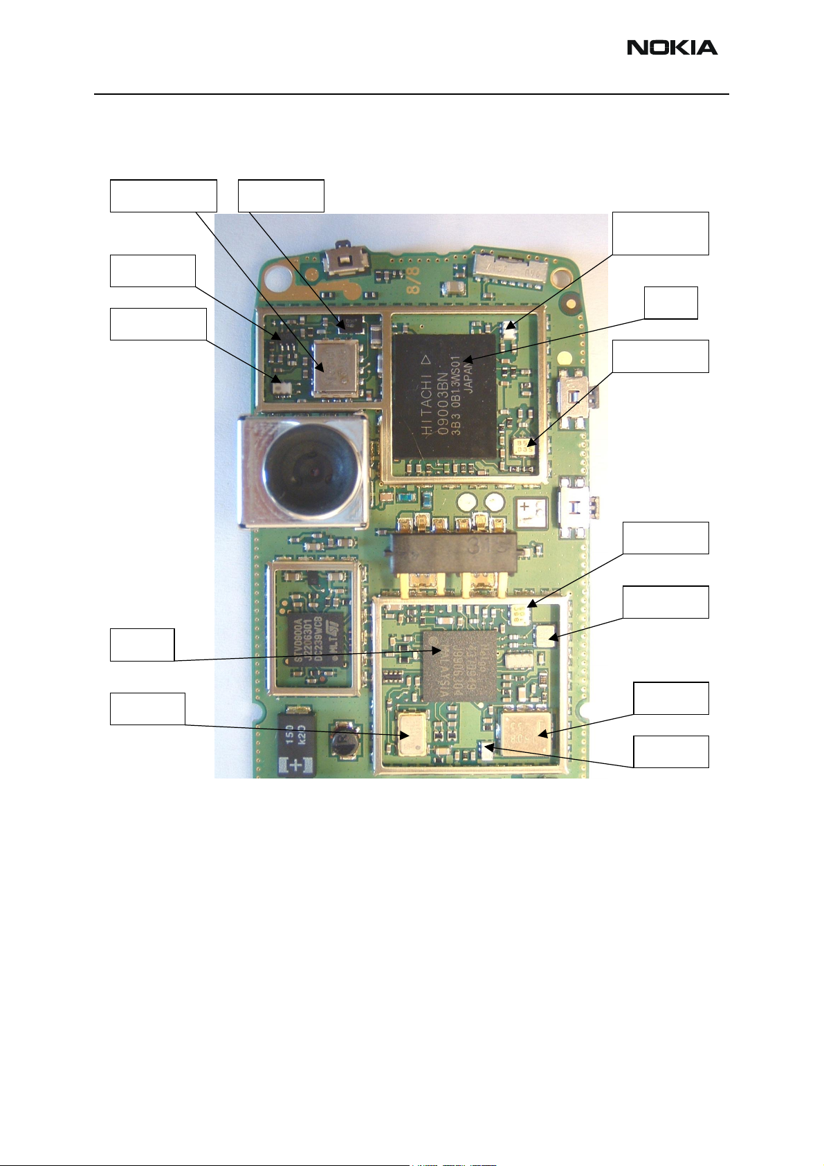
RF Key component placement
Figure 1: Component placement 1
ntenna switch
1900 RX Lna
1900 RX balun
1900 RX Saw
CCS Technical Documentation
1900/1800
TX Balun
TX 900 saw
PA
Helgo
VCTCXO
1800 RX Saw
900 RX Saw
VCO
VCO Balun
Page 6 Nokia Corporation. Issue 1 10/2003
Page 7

Company confidential RH-20
t
A
A
A
A
A
CCS Technical Documentation
RF Measurement points
To Antenna
RX 1900 saw out
VANT_2
LNA P
SM Out Rx 900
LNA VCC
VANT_3
SM out 1800Rx
VANT_1
SM In Tx1800/1900
SM In Tx900
VPECTRL3(ALC)
VR2
RFBusEn
RFBusData
RFBusRes
RFBusClk
VR1
VR3
VCTCXO outpu
TXIN/TXIP
TXQN/QP
26MHz
VBATT
Figure 2: Component placement 2
SM out 1900Rx
1800/1900 PA in
VTXB 1800/1900
Pcrtl 1800/1900
MODE
Vpcrtl 900
VTXB 900
900 PA in
I_ref_1800/1900
I_ref_900
VTXLO 900
1900 RX in
1800 RX in
VR 4
900 RX in
VR 6
TXA
TXP
VR 5
VR 7
TXC
Issue 1 10/2003 Nokia Corporation. Page 7
Page 8
RH-20 Company confidential
CCS Technical Documentation
EGSM900, GSM1800 & GSM1900 Transmitter
General instructions for Tx troubleshooting
Kindly refer to the Service Software Section, Service Concept dagram (p.40)
Connect test jig to computer with DAU-9S cable or to FPS-8 Flash Prommer with XCS-4
modular cable.
Make sure that you have PKD-1 dongle connected to computers parallel port.
Connect DC power supply to module test jig with FLC-2 cable.
Attention: When repairing or tuning transmitter use external DC supply with at
least 3A current capability. Set the DC supply voltage to 4.2V.
Connect an RF-cable to the module test jig (MJS-38) RF connector and to measurement
equipment or at least a 10dB attenuator, otherwise the PA may be damaged. Normally a
spectrum analyzer is used as measurement equipment.
Attention: Normally Spectrum analyzer maximum input power is +30dBm. It is recommended to use 10dB attenuator on Spectrum analyzer input to prevent damage.
Set the phone module to test jig and start Phoenix service sofware
Initialize connection to phone. (use FBUS driver when using DAU9S and COMBOX driver
when using FPS-8)
Select product from the menu
File -> Choose product -> RH-20
From toolbar set operating mode to "Local"
Activate RF controls window from the menu
Testing -> RF Controls
From the RF controls window
- Select band "GSM900" or "GSM 1800" or "GSM1900" (Default = "GSM900")
- Set Active unit to "Tx" (Default = "Rx")
- Set Operation mode to "Burst" (Default = "Burst")
- Set Tx data type to "Random" (Default = "All1")
- Set Rx/Tx channel to 37 on GSM900 band or 700 on GSM1800 band or 661 on
Page 8 Nokia Corporation. Issue 1 10/2003
Page 9

Company confidential RH-20
CCS Technical Documentation
GSM1900 (Defaults)
- Set Tx PA mode to "Free" (Default)
- Set power level to 5 (Default = 19) on GSM900 or to 0 (Default = 15) on GSM1800 or
GSM1900
Issue 1 10/2003 Nokia Corporation. Page 9
Page 10
RH-20 Company confidential
g
g
p
Transmitter troubleshooting diagram
CCS Technical Documentation
Yes
Yes No
Check output signal level:
+32…+33dBm@897.4MHz(GSM900)
+29…+30dBm@1747.8 and 1880MHz
(GSM1800&1900)
OK?
No
No Yes
Yes No
Check with RF probe signal level on
PA input: ~ -1…+5dBm
OK?
No
Yes
Start TX power level tuning and check tuned coefficient values:
Highest level ~0.655…0.831(GSM900); ~0.567…0.782(GSM1800&1900)
Yes
Lowest level ~0.166…0.196(GSM900); ~0.176…0.225(GSM1800&1900)
Base level ~0.137…0.166(GSM900); ~0.132…0.161(GSM1800&1900)
Major differences?
No
Check control voltage with
Yes
oscilloscope:
PA Ctrl voltage >1.5V peak
No
OK?
Yes No
TX Troubleshooting
TX signal found?
PA & Antenna Switch
troubleshooting
Figure 3: Transmitter troubleshooting
TX OK
Check
all power
levels,
OK?
Check output signal
on 500MHz span
Signal found on incorrect
frequency?
Helgo
troubleshootin
Yes
Check control loop
components
OK?
Replace faulty
com
onents
Tune
TX power
levels,
OK?
Synthesizer
troubleshootin
Tune TX coefficient
values
Replace Helgo
Page 10 Nokia Corporation. Issue 1 10/2003
Page 11
Company confidential RH-20
CCS Technical Documentation
Figure 4: HELGO IC troubleshooting
Check with oscilloscope:
-TXI/TXQ signals
No
-VR1, VR2, VR4, VR5, VR6 =2.8V
-VrefRF01 = 1.35V
-Helgo serial interface
-TXP & TXC signals
OK?
Yes
Check with RF probe:
4G VCO signal output:
No
-3589.6MHz (GSM900)
-3495.6MHz (GSM1800)
-3760MHz (GSM1900)
Level > - 10dBm
OK?
Yes
Yes
Check modulator output components
OK?
No
HELGO IC
troubleshooting
Replace faulty
component(s)
Baseband
troubleshooting
Synthesizer
troubleshooting
Replace HELGO
Issue 1 10/2003 Nokia Corporation. Page 11
Page 12
RH-20 Company confidential
p
)
p
CCS Technical Documentation
Check with RF probe signal level on PA
Yes Yes
input ~ -1…+5 dBm
OK?
Yes No
Check with oscilloscope:
-VBATT ~4V
-VTXB = 2.8V pulsed
-VPCTRL_900/1800/1900
OK?
Yes
Yes
PA & Antenna Switch
troubleshooting
No
Check components
around PA
OK?
No
Replace faulty
onent(s)
com
Figure 5: PA and Antenna Switch troubleshooting
Check with oscilloscope:
-VANT1 (GSM900)
-VANT2 (GSM1800)
-VANT3 (GSM1900)
OK?
Check VANT line
components
OK?
Yes No
Replace faulty
onent(s
com
Replace PA
Replace
HELGO
Replace ant.
switch
Page 12 Nokia Corporation. Issue 1 10/2003
Page 13
Company confidential RH-20
v
v
CCS Technical Documentation
Pictures of transmitter signals
Figure 6: Transmitter signals
TXI
VPC
200mV/di
1
VPCTRL _900 power level high at R703/C703
VPCTRL_1800/1900 power level high at R704/C704
500mV/div 100us/div
VANT_1 / GSM900 TX at C805
VANT_2 / GSM1800 TX at R804
VANT_3 / GSM1900 TX at C806 OV
( no signal/ Flatline on Oscilloscope screen)
100us/di
200mV/div
100us/div
TX I/Q at R516/517 power level high Random data
_
1
500mV/div 100us/div
VANT_1,VANT_2,VANT_3
VTXB_900 at C713
VTXB_1800_1900 at C714
Issue 1 10/2003 Nokia Corporation. Page 13
500mV/div 100us/div
500mV/div MTB 100us/div
TXP at J504
Page 14

RH-20 Company confidential
m
A
Figure 7: Tx out signal, 900 band, burst mode, channel 37
CCS Technical Documentation
Ref Lvl
Ref Lvl
34 dBm
34 dBm
34
21 dB Offset
30
20
10
0
-10
-20
-30
-40
-50
Marker 1 [T1]
28.46 dBm
897.38997996 MHz
RBW 100 kHz
VBW 100 kHz
SWT 2 s
1
RF Att 40 dB
Unit dB
A
1M
-60
-66
Center 897.4 MHz Span 2 MHz200 kHz/
Date: 28.APR.2003 15:09:42
Page 14 Nokia Corporation. Issue 1 10/2003
Page 15

Company confidential RH-20
CCS Technical Documentation
Additional information for EDGE troubleshooting
EDGE mode troubleshooting differs slightly from basic GSM troubleshooting.
Establish connection to the phone normally (see GSM900/1800/1900 troubleshooting
instructions).
Select product from the menu:
File -> Choose Product -> RH-20
From toolbar set operating mode to “Local”
Activate RF controls window from the menu:
Testing -> RF Controls
From the RF controls window:
Select Band “GSM900” or “GSM1800” or “GSM1900” (Default=”GSM900”)
Set Active unit to “Tx” (Default=”Rx”)
Set Edge “On” (Default=”Off”)
Set Operation mode to “Burst” (Default=”Burst”)
Set Tx data type to “Alternate PN9” (Default=”All1”)
Set Rx/Tx channel to 37 on GSM900 or 700 on GSM1800 or 661 on GSM1900 (Defaults)
Set power level to 8 (Default = 19) on GSM900 or to 2 (Default = 15) on GSM1800 or
GSM1900
NOTE! For GSM900 Edge power levels 5, 6 and 7 are not in use and for GSM1800&1900 Edge power
levels 0 and 1 are not in use.
Issue 1 10/2003 Nokia Corporation. Page 15
Page 16
RH-20 Company confidential
g
g
p
CCS Technical Documentation
TX EDGE Troubleshooting
Yes
Yes No
Check output signal level:
+24…+30dBm@897.4MHz(GSM900)
+22…+29dBm@1747.8 and 1880MHz
(GSM1800&1900)
OK?
No
No Yes
Yes No
Check with RF probe signal level on
PA input:
No
~-8dBm@PCL=8 (GSM900)
~-10dBm@PCL=2 (GSM1800&1900)
OK?
Yes
Start TX Edge power level tuning and check tuned coefficient values:
Highest level ~0.684…0.841(GSM900); ~0.763…0.860(GSM1800&1900)
Yes
Lowest level ~0.333…0.420(GSM900); ~0.323…0.362(GSM1800&1900)
Base level ~0.273…0.313(GSM900); ~0.244…0.313(GSM1800&1900)
Major differences?
No
Check control voltages with
Yes
oscilloscope:
Pa Iref ~2V peak (GSM900)
No
Pa Iref ~2.1V peak (GSM1800@1900)
Mode ~1.8V OK?
Yes No
TX signal found?
PA & ant switch
EDGE troubleshooting
Figure 8: Transmitter EDGE troubleshooting
TX OK
Check
all power
levels,
OK?
Check output signal
on 500MHz span
Signal found on incorrect
frequency?
Helgo EDGE
troubleshootin
Yes
Check EDGE control
loop components
OK?
Replace faulty
com
onents
Tune
TX power
levels,
OK?
Synthesizer
troubleshootin
Tune TX coefficient
values
Replace Helgo
Page 16 Nokia Corporation. Issue 1 10/2003
Page 17
Company confidential RH-20
CCS Technical Documentation
Figure 9: Helgo EDGE troubleshooting
Check with oscilloscope:
-TXI/TXQ signals
No
-VR1, VR2, VR4, VR5, VR6 =2.8V
-VrefRF01 = 1.35V
-Helgo serial interface
-TXP & TXC & TXA
OK?
Yes
Check with RF probe:
4G VCO signal output:
No
-3589.6MHz (GSM900)
-3495.6MHz (GSM1800)
-3760MHz (GSM1900)
Level > - 10dBm
OK?
Yes
Yes
Check modulator output components
and VPECTRL3 signal
No
Helgo EDGE
troubleshooting
Replace faulty
component(s)
Baseband
troubleshooting
Synthesizer
troubleshooting
Replace HELGO
Issue 1 10/2003 Nokia Corporation. Page 17
Page 18
RH-20 Company confidential
p
)
p
Figure 10: Pa & ant switch EDGE troubleshooting
PA & ant switch
EDGE troubleshooting
CCS Technical Documentation
Check with RF probe signal level on PA
input:
~ -8dBm@PCL=8 (GSM900)
~ -10dBm@PCL=2 (GSM1800&1900)
OK?
Yes No
Check with oscilloscope:
-VBATT ~4V
-Iref _900 ~2V peak
-Iref_1800_1900 ~2.1V peak
-VTXB = 2.8V pulsed
-Mode = ~1.8V
OK?
No
Check components
around PA
OK?
Yes No
Yes
Replace PA
Yes Yes
Yes
Check with oscilloscope:
-VANT1 (GSM900)
-VANT2 (GSM1800)
-VANT3 (GSM1900)
OK?
Check VANT line
components
OK?
Replace
HELGO
Replace faulty
onent(s
com
Replace ant.
switch
No
Replace faulty
onent(s)
com
Page 18 Nokia Corporation. Issue 1 10/2003
Page 19

Company confidential RH-20
CCS Technical Documentation
Pictures of EDGE transmitter signals
Figure 11: I_ref_900 power level 8 at R701/C701
Figure 12: VTXB 900 power level 8 at C713
Issue 1 10/2003 Nokia Corporation. Page 19
Page 20

RH-20 Company confidential
Figure 13: I_ref_1800/1900 power level 2 at R700/C700
CCS Technical Documentation
Figure 14: VTXB 1800/1900 power level 2 at C714
Page 20 Nokia Corporation. Issue 1 10/2003
Page 21

Company confidential RH-20
CCS Technical Documentation
Figure 15: TXA 850/1800/1900 at C538
Figure 16: TXI/TXQ signal at C535/C536/R516/R517
Issue 1 10/2003 Nokia Corporation. Page 21
Page 22

RH-20 Company confidential
Figure 17: VPECTRL3 (ALC) signal at C512
CCS Technical Documentation
Page 22 Nokia Corporation. Issue 1 10/2003
Page 23

Company confidential RH-20
CCS Technical Documentation
EGSM900, GSM1800 and GSM1900 Receiver
General instructions for Rx troubleshooting
Connect test jig to computer with DAU-9S cable or to FPS-8 Flash Prommer with XCS-4
modular cable.
Make sure that you have PKD-1 dongle connected to computers parallel port.
Connect DC power supply to module test jig with FLC-2 cable.
Set the DC supply voltage to 4.2V.
Connect an RF-cable to the module test jig (MJS-38) RF connector and to RF signal generator.
Set the phone module to test jig and start Phoenix service sofware.
Initialize connection to phone. (use FBUS driver when using DAU9S and COMBOX driver
when using FPS-8)
Choose product from the menu
File -> Choose product -> RH-20
From toolbar set operating mode to "Local"
Activate RF controls window from the menu
Testing -> RF Controls
From the RF controls window:
- Select band "GSM900", "GSM 1800" or “GSM1900” (Default = "GSM900")
- Set Active unit to "Rx" (Default = "Rx")
- Set Operation mode to "Burst" (Default = "Burst")
For continuous mode:
- Set Operation mode to "Continuous"
- Set AGC to "12: FEG_ON + DTOS_ON + BB_30=Vgain60” (maximum gain setting used
in normal mode)
(Default = "14: FEG_ON + DTOS_ON + BB_42=Vgain72")
- Set Rx/Tx channel to 37 on GSM900 band, 700 on GSM1800 band or 661 on GSM1900
Issue 1 10/2003 Nokia Corporation. Page 23
Page 24

RH-20 Company confidential
(Defaults)
Apply 942.46771 MHz (channel 37 + 67.710 kHz offset), 1842.86771 MHz (channel 700
+ 67.710 kHz offset) or 1960.06771 MHz (channel 661 + 67.71 kHz) –90 dBm signal to
the RF-connector (remember to compensate for cable attenuation).
Measuring with an oscilloscope on "RXI" or "RXQ" following screens should be seen on a
working GSM900 , GSM1800 or GSM1900 receiver:
Figure 18: RX I/Q signal ,burst mode, input level –90dBm.
CCS Technical Documentation
Receiver I or Q burst mode signal (channel 37) measured from testpoint RXI or RXQ with
942.46771 MHz signal, input level –90dBm at RF-connector.
Correct signal amplitudes approximately:
• GSM900~170mVpp
• GSM1800~140mVpp
• GSM1900~160mVpp
Signal part frequency 67.7kHz sine.
DC level of signal part is 1.35V. DC level can variate about +/-100mV between I and Q
signals and between different bands as well.
Page 24 Nokia Corporation. Issue 1 10/2003
Page 25

Company confidential RH-20
CCS Technical Documentation
Figure 19: GSM1900 RX I or Q signal (trace2), burst mode.
GSM1900 receiver burst mode I or Q signal at ch 661 with input signal 1960.067MHz,
level –90 dBm at RF-connector.
Trace2: With wider time scaling both monitoring and own RX bursts are seen, 1st burst
(shorter) is monitoring and 2nd burst (longer) is own RX burst.
Trace1: External LNA VCC supply voltage at burst mode, input level –90 dBm. Measured
from testpoint LNA_VCC.
Issue 1 10/2003 Nokia Corporation. Page 25
Page 26

RH-20 Company confidential
Figure 20: RX I&Q, phase difference 90 deg between signals.
CCS Technical Documentation
Detailed view of GSM900 continuous mode RX I and Q signals measured from testpoints
RXI and RXQ simultaneously.
Used channel 37, input signal 942.46771 MHz, level –90 dBm at antenna port, AGC setting 12.
Phase difference should be 90 degrees between RX I and Q signals at all bands.
Page 26 Nokia Corporation. Issue 1 10/2003
Page 27

Company confidential RH-20
A
q
A
–
A
)
A
CCS Technical Documentation
Troubleshooting diagram for GSM900 receiver
Phone in “Continuous” mode, AGC setting “12”
pply –90dBm
942.46771MHz signal
from generator to
antenna connector
Osilloscope at RX_I
signal 170mVpp DC
offset 1.35***
Fre
uency 67.7kHz
Rx 900 chain
functional
Check
L809,L810
Figure 21: GSM900 receiver troubleshooting
Note! Generator level can be set higher if
needed. Just note that levels will be different
in whole chain respectively.
Spectrumanalyzer:
ntenna Switch
output GSM900
88dBm
Spectrumanalyzer:
HELGO inputs
GSM900 –89dBm
Oscilloscope
VANT_1…3 0V
Check Antenna
Switch Z800
Spectrumanalyzer:
ntenna Switch
input –88dBm
Oscilloscope:Check
HELGO serial
interface (burst
mode
Check
C809
Check
Baseband
Check SAW
Z809
Check SAW
filter output
Oscilloscope:
VR1,3…6 2.7V
Check HELGO
serial interface
(burst mode)
Spectrumanalyzer:
4G VCO output
3769.6MHz
~-30dBm*
Check HELGO
N500
Check
Baseband
Synthesizer
troubleshooting
Check HELGO
N500
reading values are
measured with 1 kohm
passive probe (use
tweezers to connect the
probe ground to the nearest
PWB ground). Reading
value is represented without
+26 dB compensation.
* Spectrumanalyzer reading
with 1 kohm passive probe
(right value add +26dB)
*** DC-level of RXI/RXQ in
continuous mode will
decrase slowly. The original
level can be restored by
rewriting gain set
ll spectrumanal yzer
Issue 1 10/2003 Nokia Corporation. Page 27
Page 28

RH-20 Company confidential
A
q
A
A
)
A
Troubleshooting diagram for GSM1800 receiver
Phone in “Continuous” mode, AGC setting “12
CCS Technical Documentation
pply –90dBm
1842.86771MHz signal
from generator to
antenna connector
Osilloscope at RX_I
signal 170mVpp DC
offset 1.35***
Fre
uency 67.7kHz
Rx 1800 chain
functional
Check Z808,
L838,L839
Figure 22: GSM1800 receiver troubleshooting
Note! Generator level can be set higher if needed.
Spectrumanalyzer
ntenna Switch
output, GSM1800
-88dBm
Spectrumanalyzer
HELGO inputs
GSM1800 –88dBm
Just note that levels will be different in whole chain
respectively.
Spectrumanalyzer
input –84dBm
Oscilloscope
VANT_1…3 0V
Check Antenna
Switch Z800
ntenna Switch
Oscilloscope:Check
HELGO serial
interface (burst
mode
Check
C809
Check
Baseband
Check Z808
Check SAW
filter output
Oscilloscope
VR1,3…6 2.7V
Check HELGO
serial interface
(burst mode)
Spectrumanalyzer
4G VCO output
3685.6MHz
~-30dBm*
Check HELGO
N500
Check
Baseband
Synthesizer
troubleshooting
Check HELGO
N500
ll spectrumanalyzer
reading values are
measured with 1 kohm
passive probe (use
tweezers to connect the
probe ground to the nearest
PWB ground). Reading
value is represented without
+26 dB compensation.
* Spectrumanalyzer reading
with 1 kohm passive probe
(right value add +26dB)
*** DC-level of RXI/RXQ in
continuous mode will
decrase slowly. The original
level can be restored by
rewriting gain set
Page 28 Nokia Corporation. Issue 1 10/2003
Page 29

Company confidential RH-20
A
q
A
p
A
)
A
CCS Technical Documentation
Troubleshooting diagram for GSM1900 receiver
Phone in “Continuous” mode, AGC setting “12
Figure 23: GSM1900 receiver troubleshooting
pply –90dBm
1960.06771MHz signal
from generator to
antenna connector
Note! Generator level can be set higher
if needed. Just note that levels will be
different in whole chain respectively.
Osilloscope at RX_I
signal 160mVpp DC
offset 1.35***
uency 67.7kHz
Fre
Rx 1900 chain
functional
Spectrumanalyzer:
HELGO inputs
GSM1900 –88dBm
Check LNA
output from C829
–84dBm
Check Balun
T701 output
C808, C807
Spectrumanalyzer:
ntenna Switch
outputs, GSM1900
ut -88dBm
SAW in
Oscilloscope:
VANT_3 2.7V
VANT_1/2 0V
Spectrumanalyzer:
RX_SAW_out –
90dBm (C826)
Oscilloscope:
LNA_VCC 2.6
LNA_P 0V
Check Antenna
Switch Z800
Spectrumanalyzer:
ntenna Switch
input –84dBm
Oscilloscope:Check
HELGO serial
interface (burst
mode
Check Z806
Oscilloscope:
Check R800,
R810, L800
VR1,3…6 2.7V
Check HELGO
serial interface
(burst mode)
Check
C809
Check
Baseband
Check HELGO
N500
Check Baseband
Oscilloscope:
VR1,3…6 2.7V
Check HELGO
serial interface
(burst mode)
Spectrumanalyzer:
4G VCO output
3920 MHz
~-30dBm*
Check HELGO
N500
Check
Balun
Check
Baseband
Synthesizer
troubleshooting
Check C808,
L805, C807
Check
HELGO N500
ll spectrumanalyzer
reading values are
measured with 1 kohm
passive probe (use
tweezers to connect the
probe ground to the nearest
PWB ground). Reading
value is represented without
+26 dB compensation.
* Spectrumanalyzer reading
with 1 kohm passive probe
(right value add +26dB)
*** DC-level of RXI/RXQ in
continuous mode will
decrase slowly. The original
level can be restored by
rewriting gain set
Issue 1 10/2003 Nokia Corporation. Page 29
Page 30

RH-20 Company confidential
Synthesizer
General instructions for synthesizer troubleshooting
Connect test jig to computer with DAU9S cable or to FPS-8 Flash Prommer with XCS-4
modular cable.
Make sure that you have PKD-1 dongle connected to computers parallel port.
Connect DC power supply or FPS-8 to module test jig with PCS-1 cable.
Set the DC supply voltage to 4.2V.
Set the phone module to test jig and start Phoenix service sofware
Initialize connection to phone. (use FBUS driver when using DAU9S and COMBOX driver
when using FPS-8)
CCS Technical Documentation
Select product from the menu
File -> Choose product -> RH-20
From toolbar set operating mode to "Local"
Activate RF controls window from the menu
Testing -> RF Controls
From the RF controls window
- Select band "GSM900", "GSM 1800" or "GSM1900" (Default = "GSM900")
- Set Active unit to "Rx" (Default = "Rx")
- Set Operation mode to "Continuous" (Default = "Burst")
- Set Rx/Tx channel to 37 on GSM900 band, 700 on GSM1800 band, 661 on GSM1900
band (Defaults)
Page 30 Nokia Corporation. Issue 1 10/2003
Page 31

Company confidential RH-20
CCS Technical Documentation
Figure 24: Synthesizer troubleshooting diagram
Synthesizer
troubleshooting
*(When 2.5kOhm passive probe is used,
Yes
correct the measurement by +34 dB
Set with RF controls:
Active Unti = Rx
Operation mode = Continuous
Check with RF probe:
-4G VCO out signal
- 3589.6 MHz (GSM900)
-3495.6 MHz (GSM1800)
- 3760 MHz (GSM1900)
Level >-10dBm (*
OK ?
No
VCO out signal level<-10dBm
No
Check output signal on
1 GHz span
Signal found on
incorrect frequency ?
Yes
Yes
Synthesizer
OK
Yes
Check with oscilloscope:
-4G VCO Vcc = 2.7V
No
Check balun
output levels and
solder joints
OK ?
No
Replace
faulty
component(s)
OK ?
No
Yes
Yes
Baseband
troubleshooting
Replace
VCO
Check with oscilloscope:
VCO control voltage
from VCO pin
0V ?
No
Check with oscilloscope:
VCO control voltage
from VCO pin
>4.0 V ?
Yes
Check balun
output levels and
solder joints
OK ?
Yes
Check VCO control
loop components
Yes
OK ?
Replace
VCO
No
Replace
faulty
component(s)
No
Issue 1 10/2003 Nokia Corporation. Page 31
Page 32

RH-20 Company confidential
Pictures of synthesizer signals
Figure 25: 26MHz at G501 pin out
CCS Technical Documentation
Figure 26:
26MHz RFCLK at R420/C420
Page 32 Nokia Corporation. Issue 1 10/2003
Page 33

Company confidential RH-20
CCS Technical Documentation
Figure 27: 1800 TX, channel 512, burst mode
Figure 28: 1900 RX, channel 810, continuous mode
Issue 1 10/2003 Nokia Corporation. Page 33
Page 34

RH-20 Company confidential
Figure 29: VCO output, 1800 band, ch700, RX on, continuous output
CCS Technical Documentation
Page 34 Nokia Corporation. Issue 1 10/2003
Page 35

Company confidential RH-20
CCS Technical Documentation
Baseband troubleshooting
Figure 1: Basic baseband test points
Issue 1 10/2003 Nokia Corporation. Page 35
Page 36

RH-20 Company confidential
CCS Technical Documentation
Page 36 Nokia Corporation. Issue 1 10/2003
Page 37

Company confidential RH-20
CCS Technical Documentation
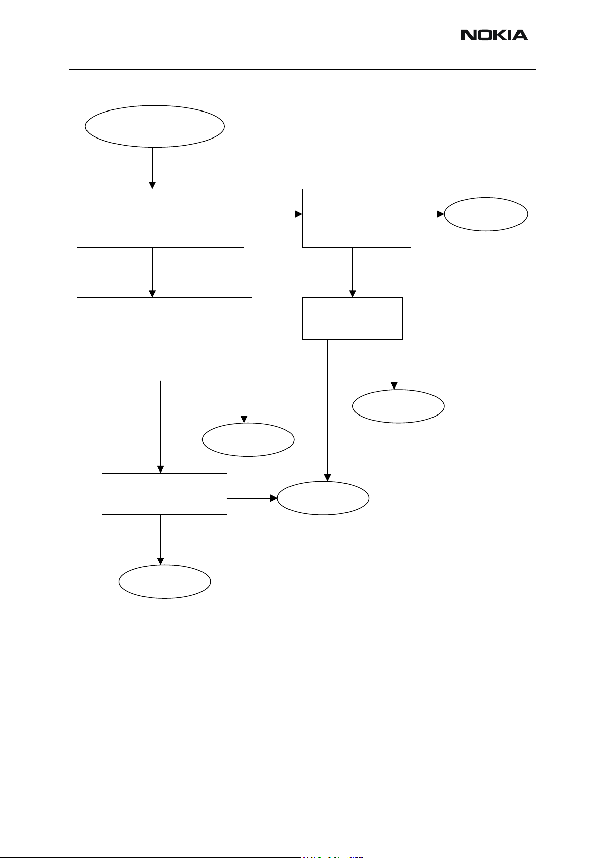
The following diagrams describe baseband troubleshooting.
Main Troubleshooting Diagram
Figure 2: Baseband general troubleshooting
Issue 1 10/2003 Nokia Corporation. Page 37
Page 38

RH-20 Company confidential
Phone is dead
Figure 3: Dead phone troubleshooting
Start
Check X100
Is phone current
0 mA?
No
Yes
(contacts,
solderings). Is it
OK?
Yes
Check L260 -
L265 and C260 -
C265. Are they
OK?
Yes
CCS Technical Documentation
No
No
Change X100
Change defect
ones
Phone current
< 50 mA
No
Phone current
~54 mA
Yes
Is phone in
LOCAL mode ?
Yes
No
No
Check all
VBATT-lines
Is flash
programming
working OK?
No
Check BSI-line including
X100,C100,C240,R202
and R206. Are they OK?
Yes
Yes
Phone is
jammed
Flash fault
Change UEM
Yes
No
Change defect part
End
Page 38 Nokia Corporation. Issue 1 10/2003
Page 39

Company confidential RH-20
CCS Technical Documentation
Flash Programming Fault
Figure 4: Flash programming troubleshooting
Start
Is the FBUS
TX-line HIGH
after startup?
Yes
Is FBUSTX-line
set to LOW after
it has been
HIGH?
Yes
Wrong
manufactor ID
and device ID
No
No
No
Measure BSI-pulse
during Flash
operation. Is it OK?
Yes
Measure FBUSTX-line
during Flash operation
(J411). Is it ~1.8V?.
Yes
Yes
No
No
Check BSI-line including
X100,C100,C240,R202
and R206.
Check R104.
If OK, change UEM
Change UPP
Change Flash
Is phone totally
dead?
No
Phone doesn't
start up or it's
jammed?
No
End (retest)
Yes
Yes
Phone is dead
Phone is
jammed
Issue 1 10/2003 Nokia Corporation. Page 39
Page 40

RH-20 Company confidential
Phone is jammed
Figure 5: Jammed phone troubleshooting (1)
Phone is jammed
CCS Technical Documentation
Measure VIO, VCORE,
VFLASH1, VANA,
VR3 voltages.
Are they OK ?
Yes
Measure 32kHz
SleepClk from t estpoint J404.
Is it OK ?
Yes
Measure 26MHz
RFClk from R420.
Is it OK ?
Check VBATT1-6
VIO,VCORE,VFLASH1,VANA,
No
No
No
VR3 lines.
Are they OK ?
Measure 32kHz
SleepClkfrom B200.
Is it OK ?
Measure 26MHz
RFCLK from G501.
Is i t OK ?
Yes
Yes
No
No
No
Check L260-265,
C260-265,
BSI/BTEMP lines and
VBATT lines
Check BSI/BTEMP
lines . If OK, change
UEM
Check B200,C209,
C210
Change UEM
Check G501,
R520,C540.
If OK change G501
Yes
Measure PURX signal
from testpoint J402.
Is it HIGH (~1.8V) ?
Yes
Phone is
jammed
2
Yes
No
Check R420, C420.
If OK change N500
Change UEM
Page 40 Nokia Corporation. Issue 1 10/2003
Page 41

Company confidential RH-20
AO
CCS Technical Documentation
Figure 6: Jammed phone troubleshooting (2)
Phone is
jammed
2
Phone Shutdown
after 30s
Yes
Measure
watchdog signal
CBUSDA from J414.
Is it OK ?
No
Change
UPP
No
Measure
CBUSClk 1MHz signal
from testpoint J406.
Is it OK ?
Yes
Read phone info.
Is i t OK ?
Yes
No
No
Yes
Retest
Measure FBUSRx
signal during phone info
read from testpoint J412.
Is it OK ?
Yes
No
Change
UEM
Measure FBUSTx
Change
UPP
Change
UEM
Change wv8
1
module or
retest
signal during phone info
read from testpoint J411.
Is it OK ?
Yes
No
Issue 1 10/2003 Nokia Corporation. Page 41
Page 42

RH-20 Company confidential
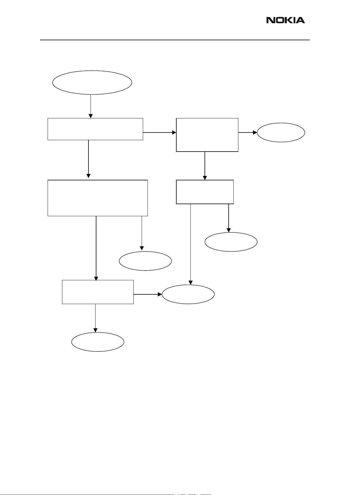
SIM card fault (Insert SIM / Card rejected)
Figure 7: SIM card troubleshooting
Start
CCS Technical Documentation
Insert SIMor
Card rejected
fault?
No
End
Yes
Set phone to LOCAL
mode. Is it OK?
Yes
Measure VSIM voltage
from X386. Is it ~3.0V?
Yes
Check SIM power-up
sequence. Is it OK?
Yes
No
No
No
Check BSI-line including
X100,C100,C240,R202 and
R206. If OK, change UEM.
Check VSIM-line
(X386,C390,R386,C203).
If OK, change R388.
If still fail, change UEM.
Check SIM lines (X386). If
OK, change R388. If still fail,
change UEM.
Change UPP
Page 42 Nokia Corporation. Issue 1 10/2003
Page 43

Company confidential RH-20
CCS Technical Documentation
Keypad Fault
Figure 8: Keypad troubleshooting (1)
Start
Is the power key
working?
Yes
Is the volume
UP key working?
Yes
Measure voltage
No No
from S302. Is it
HIGH?
Yes
Measure voltage
from S302 when
pressed. Is it
HIGH?
Yes
No
Phone is
jammed
Measure ROW0
No No
line from S300.
Is it ~1.8V?
Yes
Measure COL0
from S300 when
pressed. Is there
50us pulse?
No
Check
R306,C310,S30
2 and line. If OK,
change UEM
Check S302. Is
it OK?
Yes
No
Check S300 and line.
If OK, change Z300.If
still FAIL, change
UPP
Check S300 and
COL0 line. If OK,
change Z300.If still
FAIL, change UPP
Phone is
dead
Change S302
Change UPP
Check S301 and line.
If OK, change Z300.If
still FAIL, change
UPP
Is the volume
Down key
working?
Yes
Measure ROW1
No No
line from S301.
Is it ~1.8V?
Yes
Yes
Continue
Measure COL0
from S301 when
pressed. Is there
50us pulse?
No
Yes
Check S301 and
COL0 line. If OK,
change Z300.If still
FAIL, change UPP
Change UPP
Issue 1 10/2003 Nokia Corporation. Page 43
Page 44

RH-20 Company confidential
Figure 9: Keypad troubleshooting (2)
Continue
Try to change UI
Is the UI-module
keys working?
No
PWB. Are the
keys working
now?
No
Check X301 (solder
joints and spring
contacts). Is it OK?
Yes
No
CCS Technical Documentation
Retest failing
UI-module
Change X301
Yes
Measure ROW0 - Row4
lines from X301. Are
voltage level ~1.8V?
Yes
Measure
SLEEPX-signal from
testpoint J403 when
key is pressed.
Is voltage level
~1.8V?
Yes
When keypad is
pressed, are the
LED's turned on?
No
Check lines ROW0 -
ROW4 from X301.
No
If OK, change Z300. If
still fails, change UPP
No
Illumination
End
fault
Page 44 Nokia Corporation. Issue 1 10/2003
Page 45

Company confidential RH-20
CCS Technical Documentation
Display Fault
Start
Does the display
start?
Yes
No
Figure 10: Display troubleshooting
Try to change
UI-module. Is
the display
working now?
Yes
No
Check X302
(solder joints). Is
it OK?
No
Retest failing
UI-module
Change X302
Yes
Measure VDD (2.7V)
and VDDI (1.8V). Are
they OK?
Yes
Measure RESX(J306)
and CSX (J304)
signals. Are voltage
levels ~1.8V??
Yes
Measure SDA (J305)
and SCLK (J307)
signals. Are voltage
levels ~1.8V?
Yes
No
No
No
Check X302 and
lines again. If OK,
change UEM
Check X302 and
lines again. If OK,
change UPP
Check X302,
R308,R309 and
lines. If OK,
change UPP.
Are the display LED's
working when key is
pressed or enabled by
No
Illumination
fault
Phoenix SW?
End
Issue 1 10/2003 Nokia Corporation. Page 45
Page 46

RH-20 Company confidential
Illumination fault
Figure 11: Backlight troubleshooting
Start
CCS Technical Documentation
Are the display
LED's working?
Yes
Are the
keyboard LED's
working?
Yes
Try to change display.
No
Are the LED's working
now?
No
Check X302 (solder
joints). Is it OK?
Yes
Measure VLED+ and VLED-.
VLED+ = ~7.5V and VLED= ~0.5V when LED driver is
enabled. Are they OK?
(Notice: VLED+=VBATT
when driver is disabled)
Try to change UI PWB.
No
Are the LED's working
now?
No
Check X301 (solder
joints). Is it OK?
Yes
No
No
Yes
No
Retest failing display
Change X302
Check N300, L300, V300, R300,C303,C304.
If not OK, change defect part.
Retest failing UI PWB
Change X301
Yes
End
Measure VLED+. VLED+ =
~7.5V when LED driver is
enabled. Is it OK?
Yes
Check all LED's in UI PWB
(V101 - V106). Are they OK?
Yes
Retest
Check N300, L300, V300, R300,C303,C304.
No
No
If not OK, change defect part.
Change defect parts
Page 46 Nokia Corporation. Issue 1 10/2003
Page 47

Company confidential RH-20
CCS Technical Documentation
Charger Fault
Figure 12: Charging troubleshooting
Start
Battery bars are
working (scroll)
No
Measure voltage
over V100
(TVS).
Is it > 3.0V?
Yes
Read BTEMP value.
Compare it to ambient
temperature.
Is it ~25C?
Yes
Yes
No
No
Check X102, F100,
L100, V100, C106, C110
and line.
Check X100, C100,
R202, R207, C220
and line. Are they
OK?
Yes
No
Retest
Change defect part (if
any), re-calibrate charge
current/voltage. Retest.
Re-calibrate BTEMP with
Phoenix SW. Retest.
Change defect part,
re-calibrate and retest.
Measure charger
current throug F100.
Is it ~350...390mA
(with ACP-7)?
Yes
Retest
No Yes
Check R200. Is it
OK?
No
Change UEM
Change defect part,
re-calibrate charge
current/voltage. Retest.
Issue 1 10/2003 Nokia Corporation. Page 47
Page 48

RH-20 Company confidential
Accessory Fault
Figure 13: Accessory troubleshooting
Start
CCS Technical Documentation
Is accessory detected
when connected to
system connector?
Yes
No
Check system
connector X101
(solder ings, contact
plates). Is it OK?
Yes
Measure ACI-line
(pin3).
Is it ~0.83...1.13V?
Yes
Measure VOUT
voltage (pin4).
Is it ~2.8V?
Yes
Retest
No
No
No
Repair solderings or check contact
plates if dirty. Retest.
ACI-Accessory
Check ACI- line (L106,R103,R102,R109,C103).
If not OK, change defect part and retest.
Check VOUT-line (N100, L107, R103, C101,
C102, C112).
If not OK, change defect part and retest.
Non-ACI Accessory
End
Measure ACI-line
(pin3).
Is it ~0V?
Yes
Measure VOUT
voltage (pin4).
Is it ~0V?
Yes
Retest
No
No
Check ACI- line (L106,R103,R102,R109,C103).
If not OK, change defect part and retest.
Check that regulator N100 enable-pin is
LOW-state.
If not OK, check ACI-line again
Page 48 Nokia Corporation. Issue 1 10/2003
Page 49

Company confidential RH-20
CCS Technical Documentation
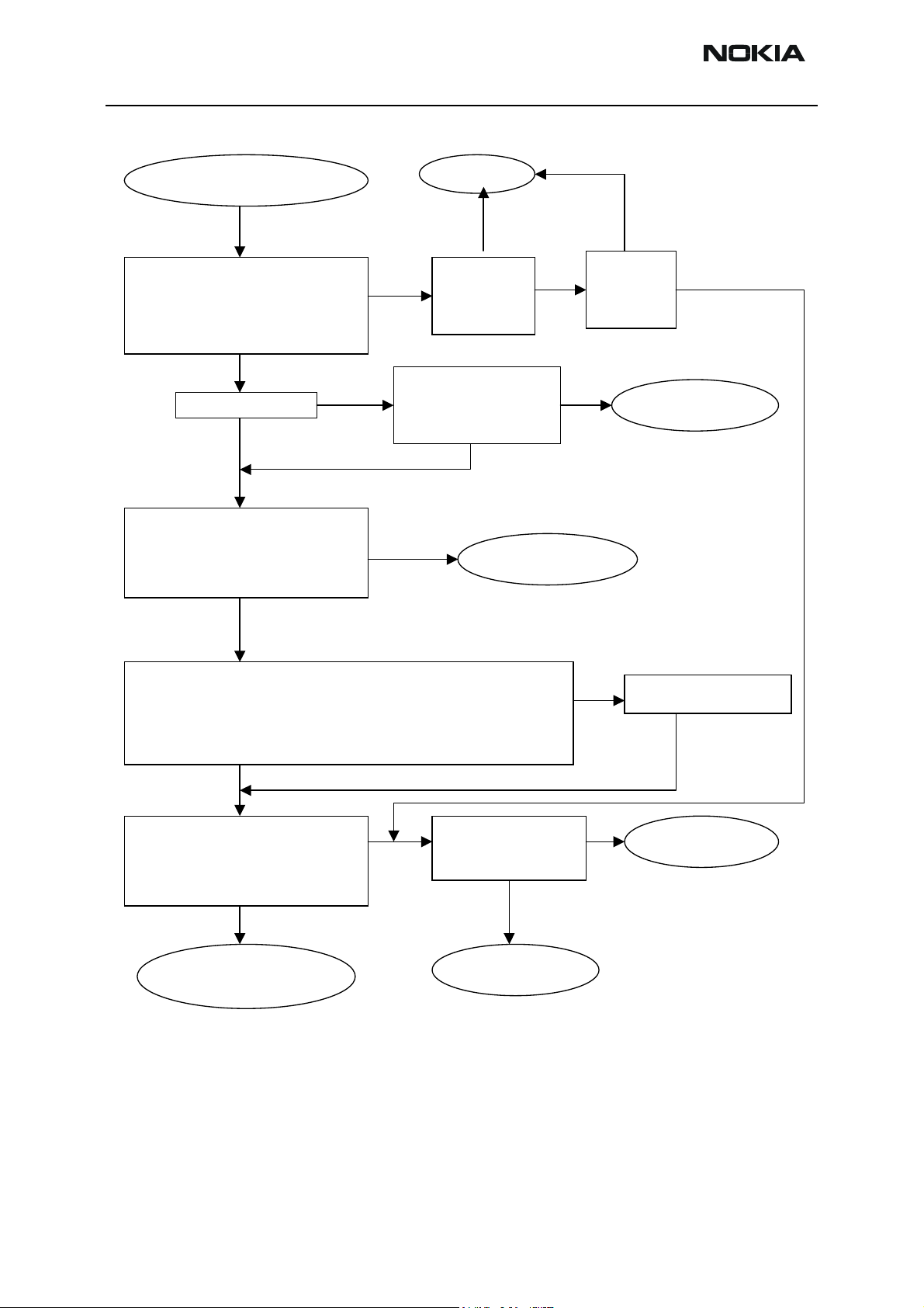
Audio Fault
Figure 14: Audio troubleshooting (1)
Audio fault s
Is earpiece
working ?
Yes
No Yes
Change old UI -module back.Set
phone to LOCAL mode. Using
Phoenix Audiotest set EXT IN, HP
Try to change
UI- module. Is it working
now ?
No
OUT, LOOP ON
Check earpiece
cont act springs from
old UI-module and
change earpiec e and
foam to old UI-
module.
Retest .
Measure DC-
offset voltage between earpiece
pads J310/J311 and GND. Is it
~1.38V ?
Yes
Measure
MICB2 voltage from
XMICP (L102 input).
Is it ~2.1V ?
Yes
No
No
Check L150, C155,
R151, R152 and line.
If OK change UEM
Check L102, C116,
C150, R153, C159,
R158 and line.
If OK change UEM.
Audio fault s
2
Earpiece
2
Issue 1 10/2003 Nokia Corporation. Page 49
Page 50

RH-20 Company confidential
Figure 15: Audio troubleshooting (2)
Earpiece
2
Connect EXT audio
signal 1kHz (s ine,
200mVpp) between
XMICP and XMICN
pads (X101, 9/10)
CCS Technical Documentation
Measure sine
signal from earpiece
pads (J310,J311).
Is It ~880mVpp ?
Yes
Change UPP
Retest
No
Measure sine
signal to UEM (R155).
Is it ~130mVpp ?
No
Yes
Check C154. If OK
change UEM
Check C154, R155,
C156, R154, C159,
R158, R159 and lines.
Page 50 Nokia Corporation. Issue 1 10/2003
Page 51

Company confidential RH-20
CCS Technical Documentation
Figure 16: Audio troubleshooting (3)
Audio fault s
2
Is microphone
working ?
Yes
Try to change new
No Yes
UI-module. Is it working
now ?
No
Restore old UI module. Set phone to
LOCAL mode. Using Phoenix
Audiotest set HP IN, EXT OUT,
LOOP ON
Measure MICB1-
voltage from MICP pad.
Is it ~2.1V ?
Yes
No
Check mic contact springs
from old UI module.
If not OK replace
microphone in old UI
module with new one.
Retest .
Check L101, C151,
C152, C153, R156,
R157.
If OK change UEM
Audio fault s
3
Check C151, R157,
C153 and line.
If OK change UEM if
still fail change UPP
Issue 1 10/2003 Nokia Corporation. Page 51
Page 52

RH-20 Company confidential
Figure 17: Audio troubleshooting (4)
Audio faults
3
CCS Technical Documentation
IHF speaker
working ?
Yes
END
Check C160,
C161, C169,
C166, R163,
L151, L152, C164
and IHF PA out put
lines .
Retest .
Try to change new C-
No
Set phone to loc al mode with Phoenix.
Set buzzer ON, vol "9" and freq. to 1kHz.
cover assembly. Is it
Restore old C-cover.
No
Yes
level between IHF
pads J156/J157 to
GND. Is it ~1.8V ?
working now?
No
Measure DC-
IHF speaker or
Yes
Check signal in C161.
contact springs
fault.
Retest .
Yes
Measure AC-
level between IHF
pads (J156,J157).
Is it ~1.0Vrms ?
No
Is it OK ?
Yes
contact springs
Yes
Check C161,
C160, R163,
C169, C170,
No
R170, C171.
change UEM
Speaker
faults.
Retest .
If OK then
Check IHF PA
controls on J152,
J153, J154.
Is it OK ?
No
Change UPP
Yes
Change IHF
PA (N150)
Page 52 Nokia Corporation. Issue 1 10/2003
Page 53

Company confidential RH-20
CCS Technical Documentation
Camera Troubleshooting
Figure 18: Component placement
Figure 19: Trace layout
Issue 1 10/2003 Nokia Corporation. Page 53
Page 54

RH-20 Company confidential
Camera Fault
Camera troubleshooting diagram
CCS Technical Documentation
Page 54 Nokia Corporation. Issue 1 10/2003
Page 55

Company confidential RH-20
CCS Technical Documentation
FM Radio troubleshooting
Figure 20: FM Radio Component layout
Figure 21: Trace layout.
Issue 1 10/2003 Nokia Corporation. Page 55
Page 56

RH-20 Company confidential
Figure 22: FM radio block layout.
Components L103, L104, L105, C107, C108, C109, C117, C162, C163, R164, R165, R166
and R167 are not shown in the picture. Those components are placed in baseband section, near audio amplifier N150.
CCS Technical Documentation
FM Radio troubleshooting diagram
Notes to "FM Radio troubleshooting diagram"
Use 1MHz 1X probe when measuring Audio and clock signals with oscilloscope.
Use active RF probe when measuring frequencies with spectrum analyzer.
Note 1. RF test signal parameters:
- Amplitude, A, –67.0 dBm
- Carrier frequency, f
- Deviation, ∆f, 75 kHz
- Modulating frequency f
- FM stereo, mode R=L, pilot state ON
, 98,000 MHz
c
, 1,000 kHz (RF generator internal)
m
Page 56 Nokia Corporation. Issue 1 10/2003
Page 57

Company confidential RH-20
CCS Technical Documentation
Figure 23: FM radio troubleshooting diagram
Set phone into local mode.
Start FM radio.
Does
the radio
start ?
YES
Connect RF test signal (note1)
Set radio channel to 98.0 MHz
Set radio volume to max.
Measure
Audio signal
from C162 and
C163.
Is it 1kHz
0.5–0.8Vp–p?
NO
Check
C107, C108,
C109, C117 ,
L105,C367,C378,
C379, L358.
Measure signal
from C162, C163
Is it 1kHz
0.5–0.8
Vp–p?
NO
Check
R359,R360,
V356, V357,
L356,L357,C357,
C358,C362.
Measure
signal from
J103, J104,
OK ?
NO
Change
N356.
Measure signal
from J103 and J104.
Is it
OK ?
Check
NO NO
YES
YES
YES
YES
C374, C375, R375,
R358 and measure
32kHz clock signal
from J359,
retest starting.
Start OK ?
YES
Check
R164,
R165, R166,
R167, L103,L104
Measure
signal from J103
and J104.
Is it
0.015–0.3
Vp–p?
YES
OK, RETEST IN FLALI
NO
Measure
voltages from
pins 7 and 34,
is it –2.7 V ?
Retest starting.
Start OK now ?
Set
Radio and RF generator
to 87.5 and 108.0 MHz.
Measure Audio from
C162 and C163.
Are both cases
1 kHz 0.5 – 0.8 Vp–p ?
NO
Check
V356, V357, L356,
L357, C357, C358, C362,
R359, R360.
T est again with
87.5 and 108.0 MHz.
Measure audio from
C162 and C163.
Both
OK?
NO
Change
V356 and 357.
BOTH !
Retest with
87.5 and 108.0 MHz.
Measure audio from
C162 and C163.
Both OK ?
NO
NO
(pins 5,6,7,8,9,11,
12,13,17,33,34,35,
Check
N356 solders
36, 37.
Start OK
now ?
YESYES
YES
YES
NO
Change
N356.
Radio start
OK
now?
NO
Baseband digital
fault (UPP)
YES
Audio
Amplifier
failure
(N150)
NO
Change
radio module TB4
OK, RETEST IN FLALI
E Nokia Corporation
Issue 1 10/2003 Nokia Corporation. Page 57
Page 58

RH-20 Company confidential
Diagrams of FM radio signals
Figure 24: Oscilloscope screen shot, Audio output
CCS Technical Documentation
Signal 1: Audio output from PWB test points J103 and J104, with FM test signal, volume
100%.
Signal 2: Audio output from FM radio pins 22 and 23(same as in C162 and C163), with
FM test signa
Figure 25: FM radio clock from test point J359, 32 kHz frequency clock signal, when radio is on.l
Page 58 Nokia Corporation. Issue 1 10/2003
Page 59

Company confidential RH-20
CCS Technical Documentation
Figure 26: FM frequency from FM radio pin 37, the other end of L358, with FM test signal
15:51:49 03 JUL 2002
PEAK
LOG
10
dB/
MKR 97.9280 MHz
#AT 0 dBREF -20.0 dBm
-71.03 dBm
SWEEP
CONT SGL
FREE RUN
VIDEO
LINE
WA SB
CORR
SC FS
CENTER 98.0000 MHz SPAN 300.0 kHz
#RES BW 10 kHz VBW 10 kHz #SWP 1.00 sec
EXTERNAL
SYNC CRD
TV TRIG
Figure 27: VCO frequency from FM radio pins 3 and 4, the other ends of V356 and V357, with FM test signal
10:46:24 03 JUL 2002
PEAK
LOG
10
dB/
WA SB
CORR
SC FS
#AT 10 dBREF .0 dBm
MKR
196.440 MHz
-9.40 dB
MEAS UNCAL
SWEEP
CONT SGL
FREE RUN
VIDEO
LINE
EXTERNAL
SYNC CRD
CENTER 196.450 MHz SPAN 1.000 MHz
#RES BW 10 kHz #VBW 10 kHz #SWP 20.0 msec
TV TRIG
Issue 1 10/2003 Nokia Corporation. Page 59
Page 60

RH-20 Company confidential
CCS Technical Documentation
This page left blank intentionally.
Page 60 Nokia Corporation. Issue 1 10/2003
 Loading...