

Page 1

Customer Care Solutions
RH-20 Series Transceivers
System Module and User
Interface
Issue 1 10/2003 Company Confidential Nokia Corporation
Page 2

RH-20 Company confidential
System Module and User Interface CCS Technical Documentation
Table of Contents
Page No
Glossary of Terms ..........................................................................................................3
Introduction ....................................................................................................................6
Electrical Modules .......................................................................................................6
Interconnection Diagram .............................................................................................6
System Module: Baseband .............................................................................................7
Baseband Module, technical summary ........................................................................7
Environmental Specifications ......................................................................................8
Temperature Conditions ............................................................................................8
Humidity and Water Resistance ................................................................................8
Baseband Technical Specifications .............................................................................9
Absolute Maximum Ratings ......................................................................................9
DC Characteristics .....................................................................................................9
Power Distribution diagram ....................................................................................11
Baseband External and Internal Signals and Connections ........................................12
FM Radio Interface .................................................................................................13
External Signals and Connections .............................................................................17
Keyboard (board-to-board) Connector ....................................................................17
LCD Connector (Board to Board) .............................................................................18
DC Connector ..........................................................................................................19
Bottom Connector ...................................................................................................19
SIM connector .........................................................................................................21
Internal Signals and Connections ............................................................................21
Baseband Functional Description ................................................................................23
Modes of Operation ...................................................................................................23
No Supply ................................................................................................................23
Back-up ...................................................................................................................23
Acting Dead .............................................................................................................23
Active ......................................................................................................................23
Sleep Mode ..............................................................................................................24
Charging ..................................................................................................................24
Battery .....................................................................................................................24
Power Up and Reset ...................................................................................................25
Power Up with PWR key ........................................................................................26
Power Up when Charger is connected ....................................................................26
Power Up when Battery is connected .....................................................................26
RTC Alarm Power Up .............................................................................................26
A/D Channels .............................................................................................................27
FM Radio ...................................................................................................................28
Camera ....................................................................................................................29
IR Module ...............................................................................................................29
SIM Interface ...........................................................................................................29
ACI ..........................................................................................................................30
External Accessory Regulator .................................................................................31
External Audio ...........................................................................................................31
External Microphone Connection ...........................................................................31
External Earphone Connections ..............................................................................32
Internal Audio ............................................................................................................33
Page 2 Nokia Corporation. Issue 1 10/2003
Page 3

Company confidential RH-20
CCS Technical Documentation System Module and User Interface
IHF Speaker & Stereo Audio Amplifier .................................................................33
Internal Microphone ................................................................................................33
Internal Speaker .......................................................................................................33
IHF Speaker & Stereo Audio Amplifier .................................................................34
Memory Block ...........................................................................................................35
Security ....................................................................................................................35
Clock distribution ......................................................................................................35
Audio Control ..........................................................................................................36
Accessory identification and Power Supply ............................................................36
Backup Battery ........................................................................................................37
RF Module Introduction ...............................................................................................38
RF Frequency Plan ....................................................................................................39
DC characteristics ......................................................................................................40
Regulators ................................................................................................................40
Typical current consumption ...................................................................................41
Power Distribution ..................................................................................................42
RF characteristics .........................................................................................................43
Channel Numbers and Frequencies .........................................................................43
Main RF characteristics ...........................................................................................43
Transmitter characteristics ......................................................................................44
Receiver characteristics ...........................................................................................44
RF Block Diagram ..................................................................................................44
RF Block Diagram RH-20 .......................................................................................45
Frequency Synthesizers .............................................................................................46
Receiver .....................................................................................................................46
Transmitter .................................................................................................................46
Other ........................................................................................................................46
Power Amplifier ......................................................................................................47
RF ASIC Helgo .......................................................................................................48
AFC function ...........................................................................................................48
Antenna ..................................................................................................................48
User interface modules ..............................................................................................49
UI board 1dm ..........................................................................................................49
Keyboard .................................................................................................................49
LCD .........................................................................................................................51
LCD & keypad illumination ....................................................................................52
Internal earpiece ......................................................................................................52
IHF ..........................................................................................................................52
Internal microphone ................................................................................................53
IR module ................................................................................................................53
Vibra ........................................................................................................................53
Pop-Port system connector ......................................................................................54
Issue 1 10/2003 Nokia Corporation. Page 3
Page 4

RH-20 Company confidential
System Module and User Interface CCS Technical Documentation
Glossary of Terms
ACI Accessory Control Interface
ADC Analog-Digital Converter
AFC Automatic Frequency Control
AGC Automatic Gain Control
API Application Programming Interface
ARM Processor architecture
ASIC Application Specific Integrated Circuit
BB Baseband
CBus Control Bus connecting UPP_WD2 with AEM and UEM
CCS Customer Care Solutions
CMT Cellular Mobile Telephone (MCU and DSP)
COG Chip On Glass
CPU Central Processing Unit
CTSI Clocking Timing Sleep Interrupt
CSP Chip Scale Package
CSTN Colour Super Twisted Nematic
DAC Digital-Analog Converter
DAI Digital Audio Interface
DB Dual band
DCT4 Digital Core Technology, 4th generation
DCN Offset Cancellation control signal
DLL Dynamic Link Library
DRC Dynamic Range Controller
DSP Digital Signal Processor
Page 4 Nokia Corporation. Issue 1 10/2003
Page 5

Company confidential RH-20
CCS Technical Documentation System Module and User Interface
EFR Enhanced Full Rate
EGPRS Enhanced General Packet Radio Service
EMC Electromagnetic compatibility
EMI Electromagnetic Interference
ESD Electro Static Discharge
EXT RF External RF
FBUS Asynchronous Full Duplex Serial Bus
GPRS General Packet Radio Service
GSM Global System for Mobile communications
HS Half Rate Speech
HSCSD High Speed Circuit Switched Data
IC Integrated Circuit
IHF Integrated Hands Free
IMEI International Mobile Equipment Identity
I/O Input/Output
IRDA Infra Red Association
LCD Liquid Crystal Display
LDO Low Drop-Out
LED Light Emitting Diode
LNA Low Noise Amplifier
MBUS 1-wire half duplex serial bus
MCU Micro Controller Unit
MDI MCU-DSP Interface
MFI Modulator and Filter Interface
Issue 1 10/2003 Nokia Corporation. Page 5
Page 6

RH-20 Company confidential
System Module and User Interface CCS Technical Documentation
PA Transmit Power Amplifier
PC Personal Computer
PCM Pulse Code Modulation
PCM SIO Synchronous serial bus for PCM audio transferring
PIFA Planar Inverted F-antenna
PWB Printed Wiring Board
PWM Pulse Width Modulation
RF Radio Frequency
RTC Real Time Clock
SIM Subscriber Identity Module
SW Software
UEM Universal Energy Management
UI User Interface
UPP Universal Phone Processor
VCXO Voltage Controlled Crystal Oscillator
VCTCXO Voltage Controlled Temperature Compensated Crystal Oscillator.
Page 6 Nokia Corporation. Issue 1 10/2003
Page 7
Company confidential RH-20
T
CCS Technical Documentation System Module and User Interface
Introduction
Electrical Modules
The system module 1AO consists of Radio Frequency (RF) and baseband (BB). User Interface (UI) contains display, keyboard, IR link, vibra, system connector and audio parts.
FM radio is located on the main PWB 1AO.
The electrical part of the keyboard is located in separate UI PWB named 1dm. 1dm is
connected to radio module PWB through a spring connector.
The Baseband blocks provide the MCU, DSP, external memory interface and digital control functions in the UPP ASIC. Power supply circuitry, charging, audio processing and RF
control hard ware are in the UEM ASIC.
The purpose of the RF block is to receive and demodulate the radio frequency signal from
the base station and to transmit a modulated RF signal to the base station.
The UI module is described in this section of the manual.
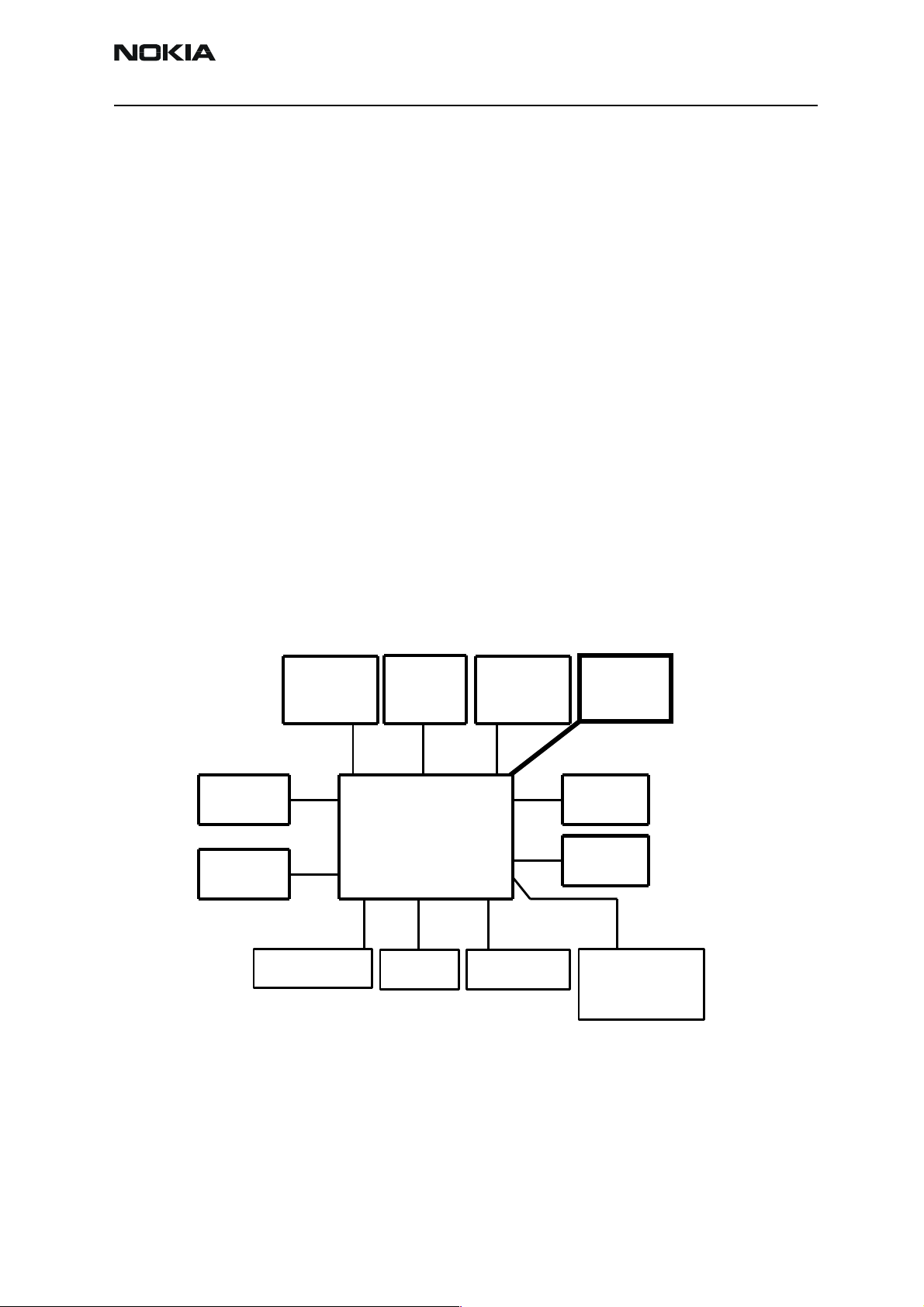
Interconnection Diagram
Keyboard
module
Antenna
Microphone
Figure 1: Interconnection diagram
Display
IHF
speaker
Radio
Module
RH-20
NHL-4
IR Link
Earpiece
CIF
Camera
BatterySIM
Charger
omahawk
Accessories
Issue 1 10/2003 Nokia Corporation. Page 7
Page 8
RH-20 Company confidential
System Module and User Interface CCS Technical Documentation
System Module: Baseband
The System module (or Engine) consists of Baseband and RF sub-modules, each described
below.
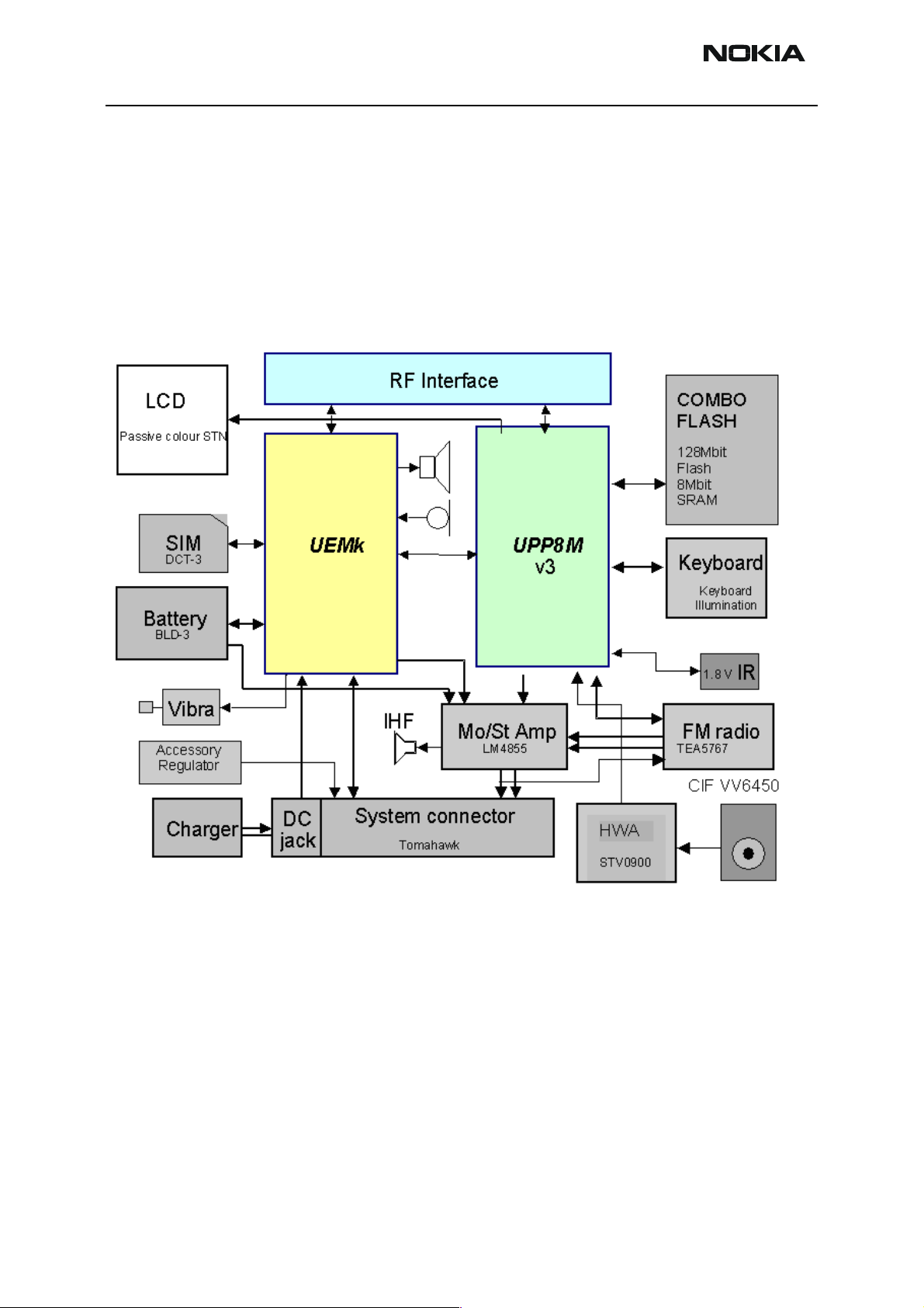
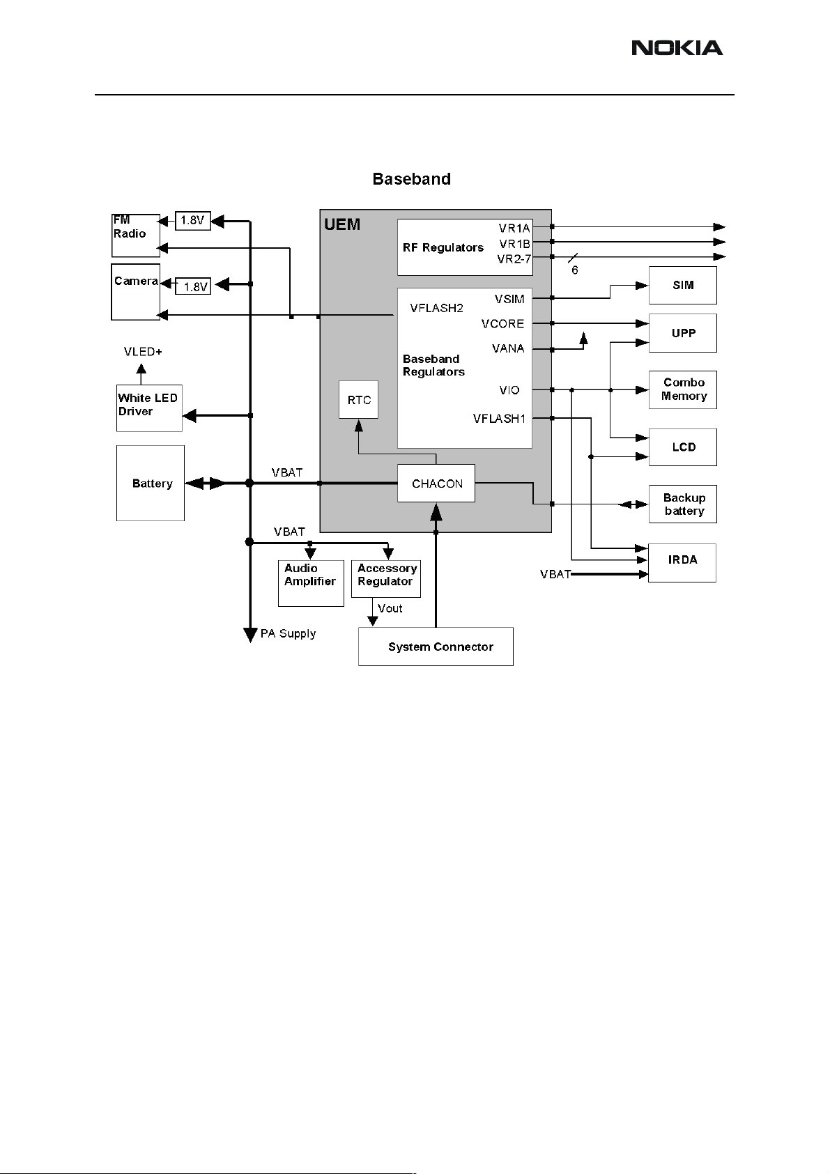
Baseband Module, technical summary
Main functionality of the baseband is implemented into two ASICs: UPP (Universal Phone
Processor) and UEM (Universal Energy Management).
Figure 2: Baseband block diagram
Baseband is running from power rails 2.8V analog voltage and 1.8V I/O voltage. UPP core
voltages can be lowered down to 1.0V, 1.3V and 1.5V. UEM includes 6 linear LDO (Low
Drop-Out) regulator for baseband and 7 regulators for RF. It also includes 4 current
sources for biasing purposes and internal usage. UEM also includes SIM interface which
supports both 1.8V and 3V SIM cards. Note: 5V SIM cards are no longer supported by
DCT-4 generation baseband.
A real time clock function is integrated into the UEM. RTC utilizes the same 32kHz clock
supply as the sleep clock. A backup power supply is provided for the RTC-battery, which
keeps the real time clock running when the main battery is removed. The backup power
supply is a rechargeable surface mounted Li-Ion battery. The backup time with the battery is 30 minutes minimum.
Page 8 Nokia Corporation. Issue 1 10/2003
Page 9

Company confidential RH-20
CCS Technical Documentation System Module and User Interface
The UEM ASIC handles the analog interface between the baseband and the RF section.
UEM provides A/D and D/A conversion of the in-phase and quadrature receive and transmit signal paths and also A/D and D/A conversions of received and transmitted audio signals to and from the user interface. The UEM supplies the analog TXC and AFC signals to
RF section according to the UPP DSP digital control. Data transmission between the UEM
and the UPP is implemented using two serial busses, DBUS for DSP and CBUS for MCU.
There are also separate signals for PDM coded audio. Digital speech processing is handled
by the DSP inside UPP ASIC. UEM is a dual voltage circuit, the digital parts are running
from the baseband supply 1.8V and the analog parts are running from the analog supply
2.78V. Also VBAT is directly used (Vibra, LED-driver, Audio amplifier).
The baseband supports both internal and external microphone inputs and speaker outputs. Input and output signal source selection and gain control is performed by the UEM
according to control messages from the UPP. Keypad tones, DTMF, and other audio tones
are generated and encoded by the UPP and transmitted to the UEM for decoding. An
external vibra alert control signals are generated by the UEM with separate PWM outputs.
RH-20 has a serial control interface: FBUS. FBUS can be accessed through a test pad and
the System Connector as described later. EMC shielding is implemented using a metallized plastic frame. On the other side, the engine is shielded with PWB grounding.
Environmental Specifications
Temperature Conditions
Full functionality through ambient temperature range -10 oC to +55 oC.
Reduced functionality between -25
Humidity and Water Resistance
Full functionality in humidity range is 5% - 95%.
Condensed or dripping water may cause intermittent malfunctions. Protection against
dripping water is implemented.
o
C to -10 oC and +55 oC to +75 oC.
Issue 1 10/2003 Nokia Corporation. Page 9
Page 10
RH-20 Company confidential
System Module and User Interface CCS Technical Documentation
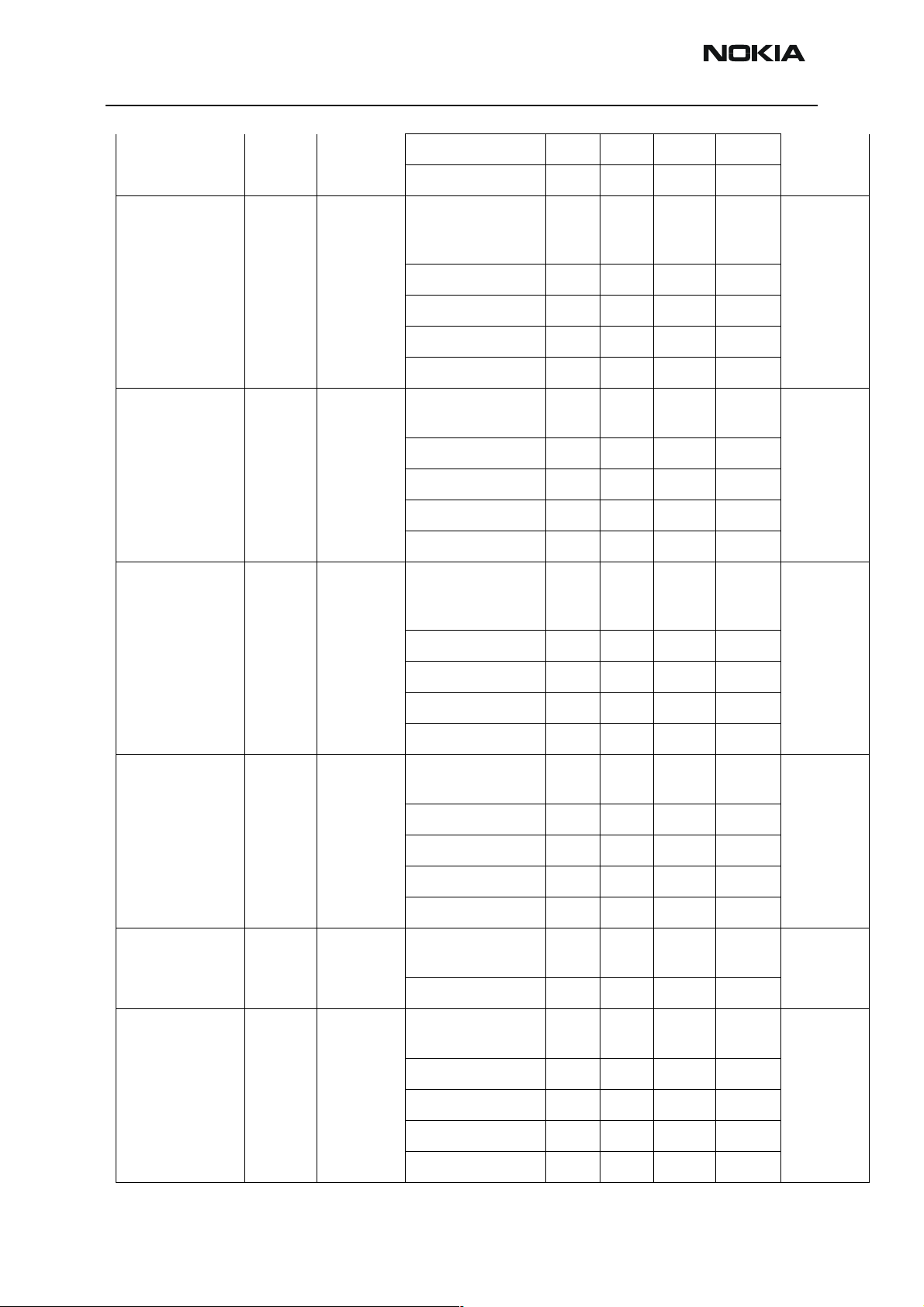
Baseband Technical Specifications
Absolute Maximum Ratings
Signal Note
Battery Voltage (Idle) -0.3V - 5.5V
Battery Voltage (Call) Max 4.7V
Charger Input Voltage -0.3V - 16V
DC Characteristics
Regulators and Supply Voltage Ranges
Battery Voltage Range
Signal Min. Nom Max Note
VBAT 3.1V 3.6V 4.2V (charging
high limit voltage)
3.1V SW cut off
BB Regulators
Signal Min. Nom Max Note
VANA 2.70V 2.78V 2.86V I
VFLASH1 2.70V 2.78V 2.86V I
VFLASH2 2.70V 2.78V 2.86V I
VSIM 1.745V
2.91V
VIO 1.72V 1.8V 1.88V I
VCORE 1.0V
1.235V
1.425V
1.710V
1.8V
3.0V
1.053V
1.3V
1.5V
1.8V
1.855V
3.09V
1.106V
1.365V
1.575V
1.890V
= 80mA
max
= 70mA
max
I
= 1.5mA
sleep
= 40mA
max
I
= 25mA
max
= 0.5mA
I
sleep
= 150mA
max
= 0.5mA
I
sleep
I
= 200mA
max
= 0.2mA
I
sleep
Default value 1.5V
Accessory Regulator
Signal Min Nom Max Note
Vout 2.72V 2.80 2.88V I
max
= 70mA
Page 10 Nokia Corporation. Issue 1 10/2003
Page 11
Company confidential RH-20
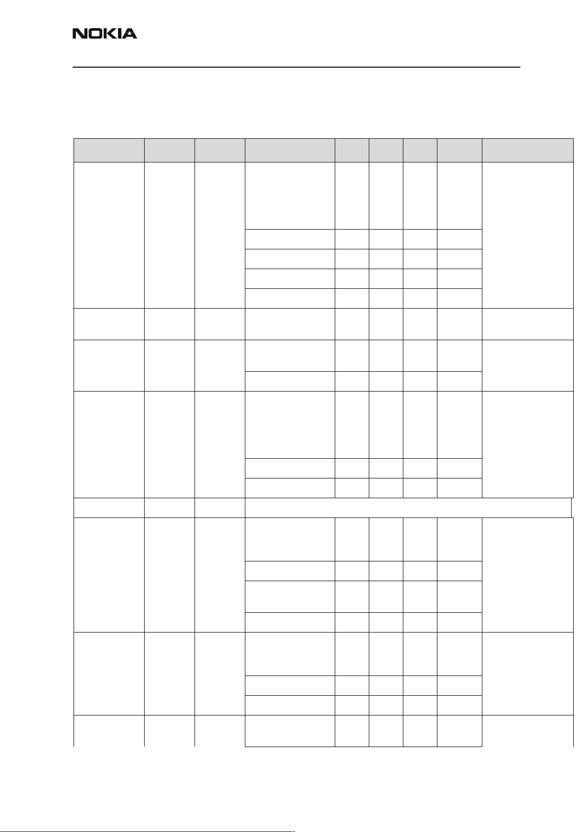
CCS Technical Documentation System Module and User Interface
RF Regulators
Signal Min Nom Max Note
VR1A 4.6V 4.75V 4.9V I
VR2 2.70V
3.20V
2.78V
3.3V
2.86V
3.40V
VR3 2.70V 2.78V 2.86V I
VR4 2.70V 2.78V 2.86V I
VR5 2.70V 2.78V 2.86V I
VR6 2.70V 2.78V 2.86V I
VR7 2.70V 2.78V 2.86V I
max
I
max
max
max
I
sleep
max
I
sleep
max
I
sleep
max
= 10mA
= 100mA
= 20mA
= 50mA
= 0.1mA
= 50mA
= 0.1mA
= 50mA
= 0.1mA
= 45mA
Current Sources
Signal Min Nom Max Note
IPA1 and IPA2 0mA - 5mA Programmable, +/-6%
V
IPA1,VIPA1
= 0V - 2.7V
IPA3 and IPA4 50µA 100µA 105µA V
= 0V - 2.7V,
IPA1
UEM Internal
Issue 1 10/2003 Nokia Corporation. Page 11
Page 12
RH-20 Company confidential
System Module and User Interface CCS Technical Documentation
Power Distribution diagram
Page 12 Nokia Corporation. Issue 1 10/2003
Page 13
Company confidential RH-20
CCS Technical Documentation System Module and User Interface
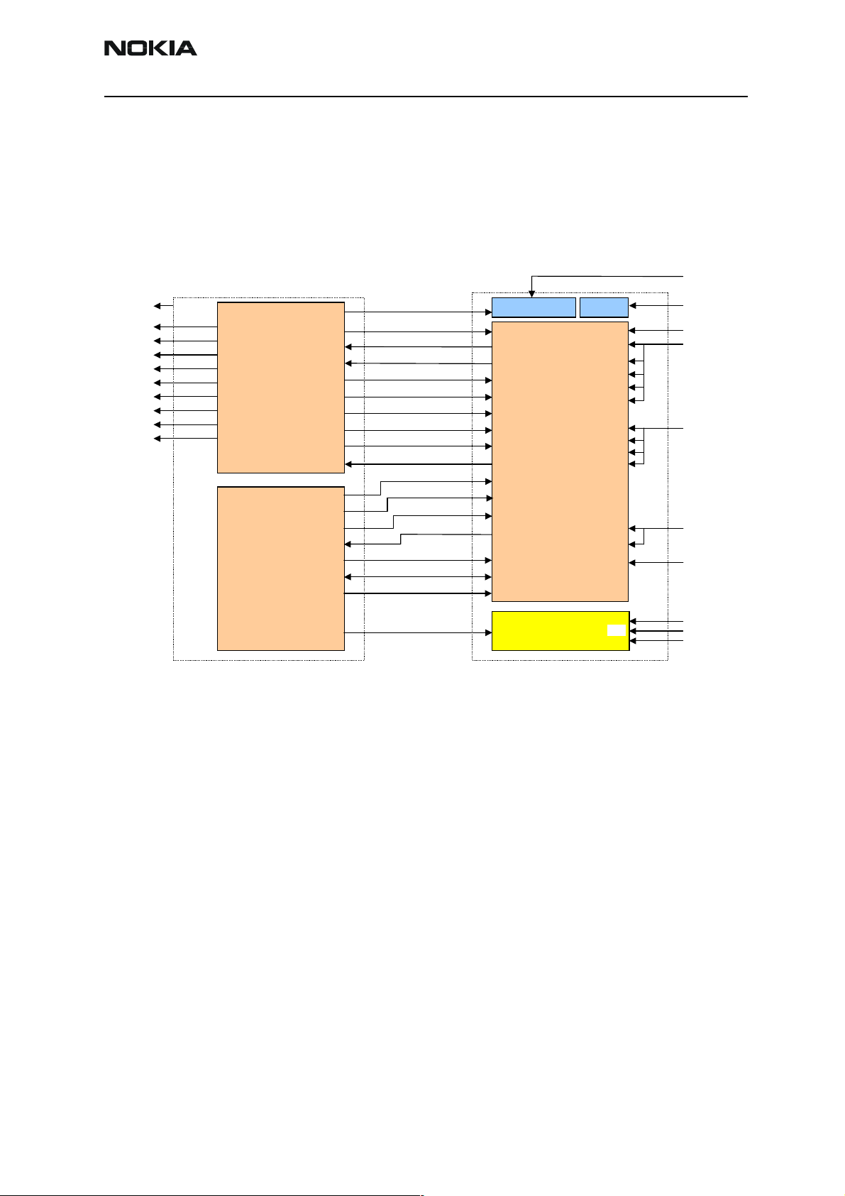
Baseband External and Internal Signals and Connections
This section describes the external and internal electrical connection and interface levels
on the baseband. The electrical interface specifications are collected into tables that
covers a connector or a defined interface.
Figure 3: RF/BB connections block diagram
VR3
VBAT
IPA1
IPA2
VR1A
VR2
VR3
VR4
VR5
VR6
VR7
BB
UEM
UPP
AFCOUT
AUXOUT
RXIINP
RXQINP
TXIOUTP
TXIOUTN
TXQOUTP
TXQOUTN
VrefRF01
PATEMP
GENIO5
GENIO6
GENIO7
RFCLK
RFBUSCLK
RFBUSDA
RFBUSEN1X
GENIO9
VCTCXO VCO
VC
TXC
OUT_BB1_I
OUT_BB1_Q
TXI_0
TXI_180
TXQ_180
TXQ_0
VB_EXT
RFTEMP
TXP
RESET
TXA
REFOUT
SCLK
SDATA
SLE
MODE
MODOUTP_G_TX
MODOUTM_G_TX
MODOUTP_P_TX
MODOUTM_P_TX
Helgo
PA
VCP
VRF_TX
VRF_RX
VF_RX
VLNA
VPAB
VLO
VPRE
VBB
900
Iref_850
Iref_1800_1900
RF
VR7
VR1A
VR2
VR4
VR5
VR6
VBAT
IPA1
IPA2
Issue 1 10/2003 Nokia Corporation. Page 13
Page 14
RH-20 Company confidential
System Module and User Interface CCS Technical Documentation
FM Radio Interface
BB Signal FM Radio Signal Min Nom Max Condition Note
VFLASH2 Vcca 2.7V 2.78V 2.86V I
Vcc(vco) 2.7V 2.78V 2.86V I
Vccd 2.7V 2.78V 2.86V I
GenIO(3) FMClk 1.4V
0
30ppm Stability
GenIO(8) FMWrEn 1.4V
0V
GenIO(12) FMCtrlDa 1.4V
0
GenIO(11) FMCtrlClk 1.4V
0
FM Antenna RFI1, RFI2 76 MHz 108 MHz FM Input frequency
1.8V 1.88V
0.4V
32kHz Frequency Also 6.5 MHz can be
1.8V 1.88V
0.4V
1.8V 1.88V
0.6V
1.8V 1.88V
0.6V
1 MHz Frequency
High
Low
High
Low
High
Low
High
Low
=10.5 mA
max
=940 µA
max
= 3.9 mA
max
Reference clock for
FM radio module
used
Write/Read enable
Bi-directional data
FM Radio L
FM Radio R
VAFL
VAFR
100mV 550mV Audio level
24 dB 30 dB Channel sep-
aration
54dB 60 dB (S+N)/N
2% Harmonic
distortion
AC and DC Characteristics of RF-Baseband Voltage Supplies
Signal
name
VBAT Battery PA, UEM Voltage 2.95 3.6 4.2 V Battery supply. Cut-off
From To Parameter Min Typ Max Unit Function
level of DCT4 regulators is
3.04V. Losses in PWB
tracks and ferrites are
taken account to minimum battery voltage
level.
Page 14 Nokia Corporation. Issue 1 10/2003
Page 15
Company confidential RH-20
CCS Technical Documentation System Module and User Interface
Current 2000 mA
Current drawn by PA
when ”off”
VR1A UEM Helgo Voltage 4.6 4.75 4.9 V Supply for charge pump
Current 2 10 mA
VR2 UEM Helgo Voltage 2.70 2.78 2.86 V Supply for I/Q-modula-
Current 65 100 mA
VR3 UEM VCTCXO,
Helgo
VR4 UEM Helgo Voltage 2.70 2.78 2.86 V Supply for Helgo RX; PA
VR5 UEM Helgo Voltage 2.70 2.78 2.86 V Supply for Helgo PLL;
Voltage 2.70 2.78 2.86 V Supply for VCTCXO, PLL
Current 1 20 mA
Current 50 mA
Current 50 mA
0.8 2 µA
for SHF VCO tuning.
tors, buffers, ALS
digital parts
bias blocks.
dividers, LO- buffers,
prescaler,
VR6 UEM Helgo Voltage 2.70 2.78 2.86 V Supply for Helgo BB and
LNAs
Current 50 mA
VR7 UEM SHF VCO Voltage 2.70 2.78 2.86 V Supply for SHF VCO
Current 30 mA
VrefRF01 UEM Helgo Voltage 1.334 1.35 1.366 V Voltage Reference for
Helgo DCN2 op.amps.
Current 100 µA
AC and DC Characteristics of RF-Baseband Digital Signals
Signal name From To Parameter Input Characteristics Function
Min Typ Max Unit
TXP
(RFGenOut3)
UPP Helgo ”1” 1.38 1.88 V Power
amplifier
enable
”0” 0 0.4 V
Load Resistance 10 220 kΩ
Issue 1 10/2003 Nokia Corporation. Page 15
Page 16
RH-20 Company confidential
System Module and User Interface CCS Technical Documentation
Load Capacitance 20 pF
Timing Accuracy 1/4 symbol
TXA UPP Helgo ”1” 1.38 1.88 V Power con-
trol loop
enable
”0” 0 0.4 V
Load Resistance 10 220 kΩ
Load Capacitance 20 pF
Timing Accuracy 1/4 symbol
RFBusEna1X UPP Helgo ”1” 1.38 1.88 V RFbus ena-
ble
”0” 0 0.4 V
Current 50 µA
Load resistance 10 220 kΩ
Load capacitance 20 pF
RFBusData UPP Helgo ”1” 1.38 1.88 V RFbus
data; read/
write
”0” 0 0.4 V
Load resistance 10 220 kΩ
Load capacitance 20 pF
Data frequency 10 MHz
RFBusClk UPP Helgo ”1” 1.38 1.88 V RFBus
clock
”0” 0 0.4 V
Load resistance 10 220 kΩ
Load capacitance 20 pF
Data frequency 10 MHz
Mode Select
(GENIO9)
UPP Helgo ”1” 1.38 1.85 V Mode
Selection
”0” 0 0.4 V
RESET
(GENIO6)
UPP Helgo ”1” 1.38 1.85 V Reset to
Helgo
”0” 0 0.4 V
Load capacitance 20 pF
Load resistance 10 220 kΩ
Timing accuracy 1/4 symbol
Page 16 Nokia Corporation. Issue 1 10/2003
Page 17
Company confidential RH-20
CCS Technical Documentation System Module and User Interface
AC and DC Characteristics of RF-Baseband Analogue Signals
Signal name From To Parameter Min Typ Max Unit Function
VCTCXO VCTCXO UPP Frequency 13 26 MHz High stability clock
signal for the logic
circuits, AC coupled. Distorted sinewave e.g. sawtooth.
Signal amplitude 0.2 0.8 2.0 Vpp
Input Impedance 10 kΩ
Input Capacitance 10 pF
Duty Cycle 40 60 %
VCTCXOGnd VCTCXO UPP DC Level 0 V Ground for refer-
ence clock
RXI/RXQ Helgo UEM Voltage swing
(static)
DC level 1.3 1.35 1.4 V
TXIP / TXIN UEM Helgo Differential voltage
swing (static)
DC level 1.17 1.20 1.23 V
Source Impedance 200 W
TXQP / TXQN UEM Helgo Same spec as for TXIP / TXIN
AFC UEM VCTCXO Voltage Min
Max
Resolution 11 bits
Load resistance
and capacitance
Source Impedance 200 W
1.35 1.4 1.45 Vpp Received demodu-
2.15 2.2 2.25 Vpp Programmable volt-
0.0
2.4
1
0.1
2.6
100
lated IQ signals
age swing.
Programmable common mode voltage.
Between TXIP-TXIN
V Automatic fre-
quency control signal for VCTCXO
kΩ
nF
TxC UEM Helgo Voltage Min
Max
Source Impedance 200 W
Resolution 10 bits
RFTemp Helgo UEM Voltage at -20oC 1,57 V Temperature sensor
2.4
0.1 V Transmitter power
level and ramping
control
of RF.
Issue 1 10/2003 Nokia Corporation. Page 17
Page 18

RH-20 Company confidential
System Module and User Interface CCS Technical Documentation
Voltage at +25oC 1,7
Voltage at +60oC 1,79
IPA1 / IPA2 UEM PA Output Voltage 0 2.7 V PA final stage quies-
cent current adjustment
Current range 0 5 mA
External Signals and Connections
Keyboard (board-to-board) Connector
Pin Signal Min. Nom Max Condition Note
1 GND 0V
2 VLED+ VBAT
7.5V
3 ROW(4) 0.7xVIO
0
4 ROW(3) 0.7xVIO
0
5 COL(2) 0.7xVIO
0
6 ROW(2) 0.7xVIO
0
7 COL(1) 0.7xVIO
0
8 ROW(0) 0.7xVIO
0
9 VLED1- 0V
1.9V
10 ROW(1) 0.7xVIO
0
11 COL(3) 0.7xVIO
0
1.8V
0.3xVIO
VIO
0.3xVIO
VIO
0.3xVIO
VIO
0.3xVIO
VIO
0.3xVIO
VIO
0.3xVIO
VIO
0.3xVIO
VIO
0.3xVIO
LED off
LED on
High
Low
High
Low
High
Low
High
Low
High
Low
High
Low
LED off
LED on
High
Low
High
Low
Supply Voltage for Keyboard LEDs
Keyboard matrix row 4
Keyboard matrix row 3
Keyboard matrix column
2
Keyboard matrix row 2
Keyboard matrix column
1
Keyboard matrix row 0
LED Katode Voltage
Keyboard matrix row 1
Keyboard matrix column
3
12 COL(4) 0.7xVIO
0
13 VLED2- 0V
1.9V
14 GND 0V
VIO
0.3xVIO
High
Low
LED off
LED on
Keyboard matrix column
4
LED Katode Voltage
Page 18 Nokia Corporation. Issue 1 10/2003
Page 19

Company confidential RH-20
CCS Technical Documentation System Module and User Interface
15 VLED3- 0V
1.9V
16 GND 0V
LED off
LED on
LED Katode Voltage
LCD Connector (Board to Board)
Table 1: LCD Connector (Board to Board)
Pin Signal Min Nom Max Condition Note
1 VDDI 1.72V 1.8V 1.88V Logic voltage
supply
Connected to
VIO
2 XRES 0.7*VDDI
0
VDDI
0.3*VDDI
Logic ’1’
Logic ’0’
Reset
Active low
1us t
3 SDA 0.7*VDDI
0
100ns t
100ns t
4 SCLK 0.7*VDDI
0
250ns t
100ns t
100ns t
5 CXS 0.7*VDDI
0
VDDI
0.3*VDDI
VDDI
0.3*VDDI
6.5MHz
VDDI
0.3*VDDI
rw
Logic ’1’
Logic ’0’
sds
sdh
Logic ’1’
Logic ’0’
Max frequency
scyc
shw
slw
Logic ’1’
Logic ’0’
Reset active
Serial data
Data setup time
Data hold time
Serial clock input
Clock cycle
Clock high
Clock low
Chip select
Active low
60ns t
css
CXS low before
SCLK rising edge
100ns t
csh
CXS low after
SCLK rising edge
Issue 1 10/2003 Nokia Corporation. Page 19
Page 20

RH-20 Company confidential
System Module and User Interface CCS Technical Documentation
6 VDD 2.70V 2.78V 2.86V Supply Voltage.
Connected to
VFLASH1
7 NC Not Connected
8 GND 0V Ground
9 VLED- 0V
0.525V
LED off
LED on
Feedback
Voltage to LED
Driver
10 VLED+ 0V
7V
LED off
LED on
Supply Voltage
for LEDs
DC Connector
Pin Signal Min. Nom Max Condition Note
1 VCHAR 11 .1 V
7.0 V
RMS
2 CHGND 0 Charger ground
8.4 V
peak
RMS
16.9 V
7.9 V
1.0 A
9.2 V
850 mA
peak
RMS
peak
RMS
Standard
charger
Fast charger
Charger positive
input
Bottom Connector
Bottom connector, or the system connector is of type Pop-Port (TM)
Figure 4: Bottom connector pinout
1
Contacts, 14 pcs
Locking holes for
accessories, 2 pcs
14
Page 20 Nokia Corporation. Issue 1 10/2003
Page 21

Company confidential RH-20
CCS Technical Documentation System Module and User Interface
Bottom connector pins and signals:
Pin/
Signal
name
1 CHARGE V Charge DC 0-9 V / 0.85 A
2 GND Charge GND 0.85 A (PWB + conn.)
3 ACI ACI 1 kbit/s Dig 0 / 2.78V Insertion & removal
4 VOUT DC out DC 2.78V / 70mA (PWB + conn.)
5 NC Not connected
6 FBUS RX FBUS 115kbit 0 / 2.78V
7 FBUS TX FBUS 115kbit 0 / 2.78V
8 GND Data GND
9 XMIC N Audio in 300 - 8k 1Vpp & 2.78V Ext. Mic Input
10 XMIC P Audio in 300 - 8k 1Vpp & 2.78V Ext. Mic Input
11 HSEAR N Audio out 20 - 20k 1Vpp Ext. audio out (left)
Signal
description
Spectral range
Voltage /
Current levels
Max or
nominal
serial
impedance
Note
detection
200mW
12 HSEAR P Audio out 20 - 20k 1Vpp Ext. audio out (left)
13 HSEAR R N Audio out 20 - 20k 1Vpp Ext. audio out
(right)
14 HSEAR R P Audio out 20 - 20k 1Vpp Ext. audio out
(right)
Issue 1 10/2003 Nokia Corporation. Page 21
Page 22

RH-20 Company confidential
System Module and User Interface CCS Technical Documentation
SIM connector
Pin Name Parameter Min. Typ Max Unit Notes
1 VSIM 1.8V SIM Card 1.6 1.8 1.9 V Supply voltage
3V SIM Card 2.8 3.0 3.2 V
2 SIMRST 1.8V SIM Card 0.9xVSIM
0
3V SIM Card 0.9xVSIM
0
3 SIMCLK Frequency 3.25 MHz SIM clock
Trise/Tfall 50 ns
1.8V Voh
1.8V Vol
3V Voh
3V Vol
4 DATA 1.8V Voh
1.8V Vol
3V Voh
3V Vol
1.8V Vih
1.8V Vil
3V Vil
3V Vil
0.9xVSIM
0
0.9xVSIM
0
0.9xVSIM
0
0.9xVSIM
0
0.7xVSIM
0
0.7xVSIM
0
VSIM
0.15xVSIM
VSIM
0.15xVSIM
VSIM V
VSIM V
VSIM
0.15xVSIM
VSIM
0.15xVSIM
VSIM
0.15xVSIM
VSIM
0.15xVSIM
V SIM reset (output)
V
V SIM data (output)
V SIM data (input)
Trise/Tfall max 1us
5 NC Not connected
6 GND GND 0 0 V Ground
Internal Signals and Connections
Page 22 Nokia Corporation. Issue 1 10/2003
Page 23

Company confidential RH-20
CCS Technical Documentation System Module and User Interface
Internal microphone
Signal Min. Nom Max Condition Note
MICP 200mV
AC 2.2kΩ to
pp
MICP
MIC1B
2.0 V 2.1 V 2.25 V DC
MICN 2.0V 2.1V 2.25V DC MICN
Internal speaker
Signal Min. Nom Max Condition Note
EARP
0.75V 0.8V
EARN
0.75V 0.8V
2.0 V
0.85V
2.0 V
0.85V
pp
AC
DC
pp
AC
Differential output
(V
= 4.0 Vpp)
diff
DC
Integrated HF speaker
Signal Min. Nom Max Condition Note
IHFP
0.75V 0.8V
IHFN
0.75V 0.8V
2.0 V
0.85V
2.0 V
0.85V
pp
AC
DC
pp
AC
Differential output
(V
= 4.0 Vpp)
diff
DC
EARP
EARN
IHFP
IHFN
Issue 1 10/2003 Nokia Corporation. Page 23
Page 24

RH-20 Company confidential
System Module and User Interface CCS Technical Documentation
Baseband Functional Description
Modes of Operation
1AO baseband has six different functional modes:
• No supply
• Back-up
• Acting Dead
• Active
• Sleep
• Charging
No Supply
In NO_SUPPLY mode, the phone has no supply voltage. This mode is due to disconnection
of main battery and backup battery or low battery voltage level in both of the batteries.
Phone is exiting from NO_SUPPLY mode when sufficient battery voltage level is detected.
Battery voltage can rise either by connecting a new battery with VBAT > V
connecting charger and charging the battery above V
Back-up
In BACK_UP mode the backup battery has sufficient charge but the main battery can be
disconnected or empty (VBAT < V
VRTC regulator is disabled in BACK_UP mode. VRTC output is supplied without regulation
from backup battery (VBACK). All the other regulators are disabled in BACK_UP mode.
Acting Dead
If the phone is off when the charger is connected, the phone is powered on but enters a
state called ”Acting Dead”. To the user, the phone acts as if it was switched off. A battery
charging alert is given and/or a battery charging indication on the display is shown to
acknowledge the user that the battery is being charged.
and VBACK > VBU
MSTR
MSTR+
COFF
or by
MSTR+
.
).
Active
In the Active mode the phone is in normal operation, scanning for channels, listening to
a base station, transmitting and processing information. There are several sub-states in
the active mode depending on if the phone is in burst reception, burst transmission, if
DSP is working etc.
One of the sub-states of the active mode is FM radio on state. In that case, Audio Amplifier and FM radio are powered on. FM radio circuitry is controlled by the MCU and
13MHz-reference clock is generated in the UPP. VFLASH2 regulator is operating.
Page 24 Nokia Corporation. Issue 1 10/2003
Page 25

Company confidential RH-20
CCS Technical Documentation System Module and User Interface
In Active mode the RF regulators are controlled by SW writing into EM’s registers wanted
settings: VR1A can be enabled or disabled. VR2 can be enabled or disabled and its output
voltage can be programmed to be 2.78V or 3.3V. VR4 -VR7 can be enabled, disabled, or
forced into low quiescent current mode. VR3 is always enabled in Active mode.
Sleep Mode
Sleep mode is entered when both MCU and DSP are in stand–by mode. Sleep is controlled by both processors. When SLEEPX low signal is detected UEM enters SLEEP mode.
VCORE, VIO and VFLASH1 regulators are put into low quiescent current mode. All the RF
regulators are disabled in SLEEP. When SLEEPX=1 detected UEM enters ACTIVE mode and
all functions are activated.
The sleep mode is exited either by the expiration of a sleep clock counter in the UEM or
by some external interrupt, generated by a charger connection, key press, headset connection etc.
In sleep mode VCTCXO is shut down and 32 kHz sleep clock oscillator is used as reference
clock for the baseband.
Charging
Charging can be performed in any operating mode.
RH-20 supports the standard NMP charger interface.
Supported chargers are ACP-7, ACP-8, ACP-12, LCH-12 and LCH-9.
Charging is controlled by the UEM ASIC and external components are needed for EMC,
reverse polarity and transient protection of the input to the baseband module. The
charger connection is through the system connector interface. The RH-20 baseband is
designed to support DCT3 chargers from an electrical point of view. Both 2- and 3-wire
type chargers are supported.
The operation of the charging circuit has been specified in such a way as to limit the
power dissipation across the charge switch and to ensure safe operation in all modes.
Battery
780 mAh Li-ion battery pack BLD-3 is used in RH-20.
Description Value
Nominal discharge cut-off voltage 3.1V
Nominal battery voltage 3.6V
Nominal charging voltage 4.2V
Maximum charger output current 850 mA
Minimum charger output current 200 mA
Issue 1 10/2003 Nokia Corporation. Page 25
Page 26

RH-20 Company confidential
System Module and User Interface CCS Technical Documentation
Pin numbering of battery pack
Signal name Pin number Function
VBAT 1 Positive battery terminal
BSI 2 Battery capacity measurement (fixed resistor inside the battery
pack)
BTEMP 3 Battery temperature measurement (measured by ntc resistor
inside pack)
GND 4 Negative/common battery terminal
Figure 5: BLD-3 battery pack pin order
Power Up and Reset
Power up and reset is controlled by the UEM ASIC. RH-20 baseband can be powered up
in following ways:
• Press power button which means grounding the PWRONX pin on UEM
• Connect the charger to the charger input
• Supply battery voltage to the battery pin.
• RTC Alarm, the RTC has been programmed to give an alarm
After receiving one of the above signals, the UEM counts a 20ms delay and then enters
its reset mode. The watchdog starts up, and if the battery voltage is greater than Vcoff+
a 200ms delay is started to allow references etc. to settle. After this delay elapses the
VFLASH1 regulator is enabled.
500us later VR3, VANA, VIO and VCORE are enabled. Finally the PURX line is held low for
20 ms. This reset, PURX, is fed to the baseband ASIC UPP, resets are generated for the
DSP and the MCU. During this reset phase the UEM forces the VCXO regulator on regardless of the status of the sleep control input signal to the UEM.
4(GND)
3(BTEMP)
2(BSI)
1 (+)
The sleep signal from the ASIC is used to reset the flash during power up and to put the
flash in power down during sleep. All baseband regulators are switched on at the UEM
power on except for the SIM regulator that is controlled by the MCU. The UEM internal
watchdog is running during the UEM reset state, with the longest watchdog time
selected. If the watchdog expires, the UEM returns to power off state. The UEM watchdog is internally acknowledged at the rising edge of the PURX signal in order to always
Page 26 Nokia Corporation. Issue 1 10/2003
Page 27

Company confidential RH-20
CCS Technical Documentation System Module and User Interface
give the same watchdog response time to the MCU.
Power Up with PWR key
When the Power on key is pressed the UEM enters the power up sequence as described in
the previous paragraph. Pressing the power key causes the PWRONX pin on the UEM to
be grounded. The UEM PWRONX signal is not part of the keypad matrix. The power key is
only connected to the UEM. This means that when pressing the power key an interrupt is
generated to the UPP that starts the MCU.
The MCU then reads the UEM interrupt register and notice that it is a PWRONX interrupt.
The MCU now reads the status of the PWRONX signal using the UEM control bus, CBUS.
If the PWRONX signal stays low for a certain time the MCU accepts this as a valid power
on state and continues with the SW initialization of the baseband. If the power on key
does not indicate a valid power on situation, the MCU powers off the baseband.
Power Up when Charger is connected
In order to be able to detect and start charging in a case where the main battery is fully
discharged (empty) and hence UEM has no supply (NO_SUPPLY or BACKUP mode of
UEM) charging is controlled by START-UP CHARGING circuitry.
Whenever VBAT level is detected to be below master reset threshold (VMSTR-) charging
is controlled by START_UP charge circuitry. Connecting a charger forces VCHAR input to
rise above charger detection threshold, VCHDET+.
By detection start-up charging is started. UEM generates 100mA constant output current from the connected charger’s output voltage. As battery charges its voltage rises,
and when VBAT voltage level higher than master reset threshold limit (VMSTR+) is
detected START_UP charge is terminated.
Monitoring the VBAT voltage level is done by charge control block (CHACON). MSTRX=‘1’
output reset signal (internal to UEM) is given to UEM’s RESET block when VBAT>VMSTR+
and UEM enters into reset sequence described in section Power Up and Reset.
If VBAT is detected to fall below VMSTR- during start-up charging, charging is cancelled.
It will restart if new rising edge on VCHAR input is detected (VCHAR rising above VCHDET+).
Power Up when Battery is connected
Baseband can be powered up by connecting battery with sufficient voltage. Battery voltage has to be over UEM internal comparator threshold level, Vcoff+. Battery low limit is
specified in Table 2. Battery Voltage Range. When battery voltage is detected, UEM
enters to reset sequence as described in section Power Up and Reset
Phone can be powered up to LOCAL mode by setting BSI resistor 560Ω. This causes MCU
to wake up directly when battery voltage is supplied.
RTC Alarm Power Up
If phone is in power off mode when RTC alarm occurs the wake up procedure is as
Issue 1 10/2003 Nokia Corporation. Page 27
Page 28

RH-20 Company confidential
System Module and User Interface CCS Technical Documentation
described in section Power Up and Reset. After baseband is powered on, an interrupt is
given to MCU. When RTC alarm occurs during power on state the interrupt for MCU is
generated.
A/D Channels
The UEM contains the following A/D converter channels that are used for several measurement purpose. The general slow A/D converter is a 10 bit converter using the UEM
interface clock for the conversion. An interrupt will be given at the end of the measurement.
The UEM’s 11-channel analog to digital converter is used to monitor charging functions,
battery functions, user interface and RF functions.
The monitored battery functions are battery voltage (VBATADC), battery type (BSI) and
battery temperature (BTEMP) indication.
The battery type is recognized through a resistive voltage divider. In phone there is a
100kΩ pull up resistor in the BSI line and the battery has a pull down resistor in the
same line. Depending on the battery type the pull down resistor value varies. The battery
temperature is measured equivalently except that the battery has a NTC pull down resistor in the BTEMP line.
KEYB1&2 inputs are used for keyboard scanning purposes. These inputs are also routed
internally to the miscellaneous block.
The monitored RF functions are PATEMP and VCXOTEMP detection. PATEMP input is used
to measure temperature of the RFIC, the Helgo.
Page 28 Nokia Corporation. Issue 1 10/2003
Page 29

Company confidential RH-20
CCS Technical Documentation System Module and User Interface
FM Radio
The FM radio in the transceiver RH-20 is a single chip electronically tuned FM stereo
radio with fully integrated IF selectivity and demodulation. The FM radio is completely
adjustment free.
It can be tuned the European, US and Japanese FM bands.
The channel tuning and bus data are controlled by UPP. A variable capacitance diode,
two coils and some resistors and capacitors are the external components for the FM
radio.
The audio frequency is fed via UEM to a headset of the phone. The FM radio antenna is
implemented in a cable of the headset.
Figure 6: FM radio
GenIO(3)
UPP8M
GenIO(12)
GenIO(11)
GenIO(8)
FMCtrlDa
FMCtrlClk
FMWrEn
FMClk
VIO
XTAL2
TEA5767
SDA
SCL
W/R
Issue 1 10/2003 Nokia Corporation. Page 29
Page 30

RH-20 Company confidential
A
r
System Module and User Interface CCS Technical Documentation
Camera
CIF camera module will be used in RH-20. Camera is connected to baseband (UPP)
through HW accelerator IC. External 1.8V regulator is used as a power supply (VDIG) for
camera module and HW accelerator together with VFLASH2.
Figure 7: Camera connections to baseband
UPP
LCDUI(1)
LCDUI(0)
GenIO(27)
GenIO(28)
GenIO(26)
GenIO(3)
LCDCamTxDa
LCDCamClk
CamRxDa
CamCSX
CamSDX
CamClk
VDIG VFLASH2
HW
ccelerato
CCISCL
CCIDA
CCPCLKN
CCPCLKP
CCPDATAN
CCPDATAP
VDIG
VFLASH2
Camera
CIF camera has a resolution of 352 x 288. Pixel size is 5.6um x 5.6um. Both camera and
HW accelerator support sleep functionality in order to minimize the current consumption.
IR Module
The IR interface when using transceiver with 1.8V I/O is designed into the UPP. The IR
link supports speeds from 9600 bit/s to 1.152 MBit/s up to distance of 80 cm. Transmission over the IR if half-duplex.
SIM Interface
UEM contains the SIM interface logic level shifting. SIM interface can be programmed to
support 3V and 1.8V SIMs. SIM supply voltage is selected by a register in the UEM. It is
only allowed to change the SIM supply voltage when the SIM IF is powered down.
The SIM power up/down sequence is generated in the UEM. This means that the UEM
generates the RST signal to the SIM. Also the SIMCardDet signal is connected to UEM.
The card detection is taken from the BSI signal, which detects the removal of the battery.
Page 30 Nokia Corporation. Issue 1 10/2003
Page 31

k
k
Company confidential RH-20
CCS Technical Documentation System Module and User Interface
The SIM interface is powered up when the SIMCardDet signal indicates "card in". This
signal is derived from the BSI signal.
Parameter Variable Min. Typ Max Unit
SIMCARDet, BSI comparator Threshold Vkey 1.94 2.1 2.26 V
SIMCARDet, BSI comparator Hysteresis (1) Vsimhyst 50 75 100 mV
The entire SIM interface locates in two chips: UPP and UEM.
The SIM interface in the UEM contains power up/down, port gating, card detect, data
receiving, ATR-counter, registers and level shifting buffers logic. The SIM interface is the
electrical interface between the Subscriber Identity Module Card (SIM Card) and mobile
phone (via UEM device).
The data communication between the card and the phone is asynchronous half duplex.
The clock supplied to the card is in GSM system 1.083 MHz or 3.25 MHz.
ACI
Figure 8: SIM interface RH-20
SIM
C5 C6 C7
C1
C3
C2
C8
C4
From
SIM
ASI P
SIMIO
SIMCl
SIMRst
VSIM
BSI
UEM
SIMIF
register
SIMIO
SIMCl
SIMRst
UEM
digital
logic
UEMInt
CBusDa
CBusEnX
CBusClk
SIMIO
SIMClk
SIMR
UIF Block
UPP
ACI is a point-to-point, bi-directional serial bus. ACI has two main features: 1)The insertion and removal detection of an accessory device 2) acting as a data bus, intended
mainly for control purposes. A third function provided by ACI is to identify and authenticate the specific accessory which is connected to the System interface.
Issue 1 10/2003 Nokia Corporation. Page 31
Page 32

RH-20 Company confidential
System Module and User Interface CCS Technical Documentation
External Accessory Regulator
An external LDO Regulator exists for accessory power supply purposes. All ACI-accessories require this power supply. Regulator input is connected to battery voltage VBAT and
output is connected to Vout pin in the system connector. Regulator is controlled via UPP
(On/Off-function).
Accessory Regulator Signals
Signal Min. Nom Max Note
Vout 2.70V 2.78 2.86V I
GenIO(0) 1.4 1.8 1.88
0.6
Figure 9: External Accessory regulation
UPP
Genio(0)
VBAT
Accessory
Regulator
System Connector
External Audio
RH-20 is designed to support fully differential external audio accessory connection by
using Pop-Port [TM] system connector. Pop-Port [TM] connector has serial data bus
called ACI (Accessory Control Interface) for accessory insertion and removal detection
and identification and authentication. ACI line is also used for accessory control purposes. See section ACI, Accessory Control Interface. Audio support from Pop-Port [TM]
system connector:
max
High (ON)
Low (OFF)
Vout
= 150mA
4-wire fully differential stereo audio (used also FM-radio antenna connection)
2-wire differential mic input
External Microphone Connection
The external microphone input is fully differential and lines are connected to the UEM
microphone input MIC2P/N. The UEM (MICB2) provides bias voltage. Microphone input
lines are ESD protected.
Creating a short circuit between the headset microphone signals generates the hook signal. When the accessory is not connected, the UEM resistor pulls up the HookInt signal.
When the accessory is inserted and the microphone path is biased the HookInt signal
decreases to 1.8V due to the microphone bias current flowing through the resistor. When
the button is pressed the microphone signals are connected together, and the HookInt
input will get half of micbias dc value 1.1 V. This change in DC level will cause the Hook-
Page 32 Nokia Corporation. Issue 1 10/2003
Page 33

p
Company confidential RH-20
CCS Technical Documentation System Module and User Interface
Int comparator output to change state, in this case from 0 to 1. The button can be used
for answering incoming calls but not to initiate outgoing calls.
Figure 10: External microphone connection
HookInt
MICB2
UEM
MIC2P
MIC2N
External Earphone Connections
Headset implementation uses separate microphone and earpiece signals. The accessory is
detected by the HeadInt signal when the plug is inserted (see section ACI, Accessory
Control Interface).
Figure 11: External Earphone & IHF Connections
FM Radio
VAFR
VAFL
MIC3P
UEM
MIC3N
XEAR
Audio
Audio amplifier
Rin
Lin
SPKRout+
SPKRout-
PhoneIN (HS)
PhoneIN
(IHS)
Rout+
RoutLout+
Lout-
EMC/ESD
Com
onents
EMC/ESD
Components
XMICP
XMICN
IHF Speaker
When the accessory is inserted and the microphone path is biased the HookInt signal
decreases to 1.8V due to the microphone bias current flowing through the resistor. When
the button is pressed the microphone signals are connected together, and the HookInt
input will get half of micbias dc value 1.1 V. This change in DC level will cause the HookInt comparator output to change state, in this case from 0 to 1. The button can be used
for answering incoming calls but not to initiate outgoing calls.
Issue 1 10/2003 Nokia Corporation. Page 33
Page 34

RH-20 Company confidential
System Module and User Interface CCS Technical Documentation
Internal Audio
IHF Speaker & Stereo Audio Amplifier
Integrated Hands Free Speaker, 16mm MALT, is used to generate speech audio, alerting
and warning tones in RH-20. Audio amplifier is controlled by the UPP. Speaker capsule is
mounted in the C-cover. Spring contacts are used to connect the IHF Speaker contacts to
the main PWB.
Figure 12: IHF speaker and amplifier
Internal Microphone
The internal microphone capsule is mounted to in the UI-frame. Microphone is omni
directional and it’s connected to the UEM microphone input MIC1P/N. The microphone
input is asymmetric and the UEM (MICB1) provides bias voltage. The microphone input
on the UEM is ESD protected. Spring contacts are used to connect the microphone to the
main PWB.
Figure 13: Internal microphone
Internal Speaker
The internal earpiece is a dynamic earpiece with impedance of 32 ohms. The earpiece
must be low impedance one since the sound pressure is to be generated using current
and not voltage as the supply voltage is restricted to 2.7V. The earpiece is driven directly
by the UEM and the earpiece driver in UEM is a bridge amplifier. In RH-20 8mm PICO
Page 34 Nokia Corporation. Issue 1 10/2003
Page 35

K
A
Company confidential RH-20
CCS Technical Documentation System Module and User Interface
type earpiece is used.
Figure 14: Internal speaker
EARP
UEM
EARN
IHF Speaker & Stereo Audio Amplifier
Integrated Hands Free Speaker, 16mm MALT, is used to generate speech audio, alerting
and warning tones in RH-20. Audio amplifier is controlled by the UPP. Speaker capsule is
mounted in the C-cover. Spring contacts are used to connect the IHF Speaker contacts to
the main PWB.
Figure 15: Digital Interface of Audio Amplifier
Common mode
choke
VBAT
Phone In IHF
Phone In HS
Bypass
Rin
Lin
Bias
Digital
Volume
Control
=
EN CL
Output
Mode
Select
SPI
DAT
Amplifier
Amplifier
Amplifier
GND
IHF Speaker
out +
out -
Rout +
Rout -
Lout +
Lout -
Stereo Headset
Issue 1 10/2003 Nokia Corporation. Page 35
Page 36

RH-20 Company confidential
System Module and User Interface CCS Technical Documentation
Memory Block
For the MCU UPP includes ROM, 8 kbytes, that is used mainly for boot code of MCU. To
speed up the MCU operation small 4 kbyte cache is also integrated as a part of the MCU
memory interface. For program memory 8Mbit (512 x 16bit) PDRAM is integrated. RAM
block can also be used as data memory and it is byte addressable. RAM is mainly for MCU
purposes but also DSP has also access to it if needed.
In addition to UPP integrated RAM RH-20 baseband has also UPP external SRAM. This is
implemented in combo memory (single package with stacked ICs, 128Mbit flash + 8 Mbit
SRAM).
MCU code is stored into external flash memory. Size of the flash is 128Mbit (8192 x
16bit) The HDi 13 baseband supports a burst mode flash with multiplexed address/data
bus. Access to the flash memory is performed as 16–bit access. The flash has Read While
Write capabilities which makes the emulation of EEPROM within the flash easy.
Security
The phone flash program and IMEI codes are software protected using an external security device that is connected between the phone and a PC.
Clock distribution
32 kHz
UEM
Figure 16: Clock Distribution Diagram
VR3
VCTCXO
26MHz
32 kHz
26 MHz
UPP
SLEEPX
SLICER
HELGO
HELGA
26 MHz
RFBUSCLK 13MHz
CBUSCLK 1MHz
MCU
DSP
PLL
CTSI
DBUSCLK 13MHz
LCDCLK max. 6.5MHz
SIMCLK max. 3.25MHz
Page 36 Nokia Corporation. Issue 1 10/2003
Page 37

Company confidential RH-20
CCS Technical Documentation System Module and User Interface
Audio Control
Figure 17: Audio block diagram RH-20
earpiece
Tomahawk
bottom connector
microfone
Mic
ACI
Phs
Pihf
Lin
Rin
Lout
Rout
IHFSpeaker
SPKR
Lout
Rout
PA
Accessory identification and Power Supply
Figure 18: Accessory identification and Power supply
UEM
earp
mic1
mic2
headint
xear
mic3
Control Bus
ear data
mic data
Radio
L
antenna
R
UPP
Vhead
Vflash1
4.7k
Vflash1
headint=
UEM
HEADINT
ACI
switch
MBUS
UPP
Vflash1
Enable
100k
VBatt
Accessory
Regulator
2.8V/70mA
ACI-line
Vout
Tomahawk
56k
ACI
Chip
Issue 1 10/2003 Nokia Corporation. Page 37
Page 38

RH-20 Company confidential
System Module and User Interface CCS Technical Documentation
Backup Battery
Backup battery is used in case when main battery is either removed or discharged.
Backup battery is used for keeping real-time clock running for minimum of 30 minutes.
Rechargeable backup battery is connected between UEM VBACK and GND. In UEM
backup battery charging high limit is set to 3.2V. The cut–off limit voltage (V BUCoff–)
for backup battery is 2.0V. Backup battery charging is controlled by MCU by writing into
UEM register.
Li-Ion SMD battery type is used. The nominal capacity of the battery is 0.01 mAh.
Table 28. Backup Battery circuitry
Parameter
Test conditions
Back-up battery voltage VBACK 2.43 3.3 V
Back-up battery cut-off limit V_BU
Charging voltage (VBAT ≥ 3.4V)
Charging current I
Symbol Min Typ Max Units
COFF+
V_BU
COFF-
VBU 3.1 3.2 3.3 V
LIMVBU
2.04
1.94
150 500 mA
2.10
2.0
2.16
2.06
V
V
Page 38 Nokia Corporation. Issue 1 10/2003
Page 39

Company confidential RH-20
CCS Technical Documentation System Module and User Interface
RF Module Introduction
The RF module performs the necessary high frequency operations of the EGSM900/
GSM1800/GSM1900 tripleband (EDGE) engine. Both the transmitter and receiver have
been implemented by using direct conversion architecture which means that the modulator and demodulator operate at the channel frequency.
The core of the RF is an application-specific integrated circuit, Helgo. Another core component is a power amplifier module which includes two amplifier chains, one for
EGSM900 and the other for GSM1800/GSM1900.
Other key components include
• 26 MHz VCTCXO for frequency reference
• 3420-3980 MHz SHF VCO (super high frequency voltage controlled oscillator)
• front end module comprising a RX/TX switch
• four additional SAW filters
The control information for the RF is coming from the baseband section of the engine
through a serial bus, referred later on as RFBus. This serial bus is used to pass the information about the frequency band, mode of operation, and synthesizer channel for the RF.
In addition, exact timing information and receiver gain settings are transferred through
the RFBus. Physically, the bus is located between the baseband ASIC called UPP and
Helgo. Using the information obtained from UPP Helgo controls itself to the required
mode of operation and further sends control signals to the front end and power amplifier
modules. In addition to the RFBus there are still other interface signals for the power
control loop and VCTCXO control and for the modulated waveforms.
RF circuitry is located on one side of the 8 layer PWB.
EMC leakage is prevented by using a metal cans. The RF circuits are separated to three
blocks.
• FM radio.
• PA, front end module, LNA, 1900 band Rx SAWs and 900 Tx SAW.
• Helgo RF IC, VCO, VCTCXO, baluns and 1800 and 1900 Rx SAWs.
The RF transmission lines constitute of striplines and microstriplines after PA.
The baseband circuitry is located on the one side of the board, which is shielded with a
metallized frame and ground plane of the UI-board.
Issue 1 10/2003 Nokia Corporation. Page 39
Page 40

RH-20 Company confidential
3420
System Module and User Interface CCS Technical Documentation
RF Frequency Plan
RF frequency plan is shown below. The VCO operates at the channel frequency multiplied
by two or four depending on the frequency band of operation. This means that the baseband modulated signals are directly converted up to the transmission frequency and the
received RF signals directly down to the baseband frequency.
Figure 19: RF Frequency plan
925-960
925-960
MHz
1805-1990
MHz
1710-1910
MHz
880-915
880-915
MHz
f/4
HELGO
HELGA
f
f
I-signal
I-signalI-signalI-signal
Q-signal
RX
f/2f/4
f
f/2
f
-
3420-
PLL
3980
MHz
26 MHz
VCTCXO
I-signal
Q-signal
TX
Page 40 Nokia Corporation. Issue 1 10/2003
Page 41

Company confidential RH-20
CCS Technical Documentation System Module and User Interface
DC characteristics
Regulators
The transceiver baseband section has a multi function analog ASIC, UEM, which contains
among other functions six pieces of 2.78 V linear regulators and a 4.8 V switching regulator. All the regulators can be controlled individually by the 2.78 V logic directly or
through a control register. Normally, direct control is needed because of switching speed
requirement: the regulators are used to enable the RF-functions which means that the
controls must be fast enough.
The use of the regulators can be seen in the power distribution diagram which is presented in Figure 20, “Power distribution diagram,” on page 43.
The seven regulators are named VR1 to VR7. VrefRF01 and VrefRF02 are used as the reference voltages for the Helgo, VrefRF01 (1.35V) for the bias reference and VrefRF02
(1.35V) for the RX ADC (analog-to-digital converter) reference.
The regulators (except for VR7) are connected to the Helgo. Different modes of operation
can be selected inside the Helgo according to the control information coming through
the RFBus.
List of the needed supply voltages
Volt. source Load
VR1 PLL charge pump (4.8 V)
VR2 TX modulators, VPECTRL3s (ALC), driver
VR3 VCTCXO, synthesizer digital parts
VR4 Helgo pre-amps, mixers, DtoS
VR5 dividers, LO-buffers, prescaler
VR6 LNAs, Helgo baseband (Vdd_bb)
VR7 VCO
VrefRF01 ref. voltage for Helgo
VrefRF02 ref. voltage for Helgo
Vbatt PA
Issue 1 10/2003 Nokia Corporation. Page 41
Page 42

RH-20 Company confidential
System Module and User Interface CCS Technical Documentation
Typical current consumption
The table shows the typical current consumption in different operation modes.
Operation mode Current consumption Notes
Power OFF < 10 uA Leakage current (triple band PA)
RX, EGSM900 75 mA, peak
RX, GSM1800/GSM1900 70 mA, peak
TX, power level 5, EGSM900 1600 mA, peak
TX, power level 0, GSM1800/
GSM1900
900 mA, peak
Page 42 Nokia Corporation. Issue 1 10/2003
Page 43

Company confidential RH-20
CCS Technical Documentation System Module and User Interface
Power Distribution
Figure 20: Power distribution diagram
HELGO
LNA
GSM1800/
GSM1900
1900
Issue 1 10/2003 Nokia Corporation. Page 43
Page 44

RH-20 Company confidential
System Module and User Interface CCS Technical Documentation
RF characteristics
Channel Numbers and Frequencies
System Channel number TX frequency RX frequency Unit
EGSM900 0 < =n <=124 F = 890 + 0.2 * n F = 935 + 0.2 * n MHz
975<= n <= 1023 F= 890+0.2* (n -1024) F= 935+0.2* (n -1024) MHz
GSM1800 512 <= n <= 885 F=1710.2+0.2*(n-512) F=1805.2+0.2*(n-512) MHz
GSM1900 512 <= n <=810 F=1850.2+0.2*(n-512) F=1930.2+0.2*(n-512) MHz
Main RF characteristics
Parameter Unit and value
Cellular system EGSM900/GSM1800/GSM1900
RX Frequency range EGSM900: 925 ... 960 MHz
GSM1800: 1805...1880 MHz
GSM1900: 1930...1990 MHz
TX Frequency range EGSM900: 880 ... 915 MHz
GSM1800: 1710 ...1785 MHz
GSM1900: 1850 …1910 MHz
Duplex spacing EGSM900: 45 MHz
GSM1800: 95 MHz
GSM1900: 80 MHz
Channel spacing 200 kHz
Number of RF channels EGSM900: 174
GSM1800: 374
GSM1900: 300
Output Power EGSM900: GSMK 5…33 dBm
EGSM900: 8-PSK 5…27 dBm
GSM1800: GSMK 0…30 dBm
GSM1800: 8-PSK 0…26 dBm
GSM1900: GSMK 0…30 dBm
GSM1900: 8-PSK 0…26 dBm
Number of power levels GSMK EGSM900: 15
GSM1800: 16
GSM1900: 16
Number of power levels 8-PSK EGSM900: 12
GSM1800: 14
GSM1900: 14
Page 44 Nokia Corporation. Issue 1 10/2003
Page 45

Company confidential RH-20
CCS Technical Documentation System Module and User Interface
Transmitter characteristics
Item Values (EGSM900/GSM1800/GSM1900)
Type Direct conversion, nonlinear, FDMA/TDMA
LO frequency range 3520...3660 MHz/3420...3570 MHz/3700...3820 MHz
Output power GMSK 33/30/30 dBm
8-PSK 27/26/26 dBm
Gain control range min. 30 dB
Phase error (RMS/peak), GMSK
EVM (RMS/peak), 8-PSK
5 deg./20 deg. peak
10%/30%
Receiver characteristics
Item Values, EGSM900/GSM1800/GSM1900
Type Direct conversion, Linear, FDMA/TDMA
LO frequencies 3700...3840 MHz / 3610...3760 MHz/3860...3980 MHz
Typical 3 dB bandwidth +/- 91 kHz
Sensitivity min. - 102 dBm (normal condition)
Total typical receiver voltage gain (from antenna
to RX ADC)
Receiver output level (RF level -95 dBm) 230 mVpp, single-ended I/Q signals to RX ADCs
Typical AGC dynamic range 83 dB
Accurate AGC control range 60 dB
Typical AGC step in LNA 30 dB GSM1800/GSM1900 25 dB EGSM900
86 dB
Usable input dynamic range -102... -10 dBm
RSSI dynamic range -110... -48 dBm
Compensated gain variation in receiving band +/- 1.0 dB
RF Block Diagram
The block diagram of the RF module can be seen in Chapter on “RF Block Diagram”. The
detailed functional description is given in the following sections
Issue 1 10/2003 Nokia Corporation. Page 45
Page 46

RH-20 Company confidential
System Module and User Interface CCS Technical Documentation
RF Block Diagram RH-20
Figure 21: RF Block Diagram
THIS DRAWING CONTAINS PROPRIETARY AND CONFIDENTIAL INFORMATION.
THIS DRAWING IS PROTECTED BY COPYRIGHT AS AN UNPUBLISHED WORK.
UNAUTHORIZED REPRODUCTION OF THIS DRAWING IS NOT PERMITTED.
Copyright (C) Nokia Corporation. All rights reserved.
This document is property of Nokia Corporation
File
Assoc
Proj
HDi13 Jesse
/disks/jesse/product_imp/electronics/pwb/block_diagram
Sheet of
Print
Yes
V.Drw.
1.0
yyxx
Edit
(01)1
70
Name
RF/BB module RH-20
RF block diagram
Appr
Des.
Dr.
LEIPALA
LEIPALA
dd-mmm-yy
17-Aug-99
27-May-03
Page 46 Nokia Corporation. Issue 1 10/2003
Page 47

CCS Technical Documentation System Module and User Interface
Company confidential RH-20
Frequency Synthesizers
The VCO frequency is locked by a PLL (phase locked loop) into a stable frequency source
given by a VCTCXO which is running at 26 MHz. The frequency of the VCTCXO is in turn
locked into the frequency of the base station with the help of an AFC voltage which is
generated in UEM by an 11 bit D/A converter. The PLL is located in Helgo and it is controlled through the RFBus.
The required frequency dividers for modulator and demodulator mixers are integrated in Helgo.
Loop filter filters out the comparison pulses of the phase detector and generates a DC
control voltage to the VCO. The loop filter determines the step response of the PLL (settling time) and contributes to the stability of the loop.
The frequency synthesizer is integrated in Helgo except for the VCTCXO, VCO, and the
loop filter.
Receiver
Each receiver path is a direct conversion linear receiver. From the antenna the received
RF-signal is fed to a front end module where a diplexer first divides the signal to two
separate paths according to the band of operation: either lower, EGSM900 or upper,
GSM1800/GSM1900 path.
Most of the receiver circuitry is included in Helgo.
Transmitter
The transmitter consists of two final frequency IQ-modulators and power amplifiers, for
the lower and upper bands separately, and a power control loop. The IQ-modulators are
integrated in Helgo, as well as the operational amplifiers of the power control loop. The
two power amplifiers are located in a single module with power detector. In the GMSK
mode the power is controlled by adjusting the DC bias levels of the power amplifiers. In
EDGE mode, the power is controlled by adjusting ALC in Helgo RFIC.
Other
Other key blocks are:
- Antenna 50 ohm input
- Antenna switch module
- RX EGSM900/GSM1800 balaned output, GSM1900 single output
- TXs single 50 ohm input
-3 control lines from the Helgo
Issue 1 10/2003 Nokia Corporation. Page 47
Page 48

RH-20 Company confidential
System Module and User Interface CCS Technical Documentation
Figure 22: Front End
Ant
TX
TX
EGSM900
EGSM
TX GSM
TX
1800/1900
DCS/PCS
RX
RX
GSM1900
PCS
RX
RX
GSM1800
DCS
RX
RX
EGSM900
EGSM
Power Amplifier
The power amplifier features include:
- 50 ohm input and output, EGSM900/GSM1800/GSM1900
- internal power detector
- EDGE mode
Page 48 Nokia Corporation. Issue 1 10/2003
Page 49

/
/
GS
/
Company confidential RH-20
CCS Technical Documentation System Module and User Interface
Figure 23: Power amplifier
EGSM900
EGSM
out
GSM1800
DCS/
1900
PCS
out
EGSM900
EGSM
Power
control
GSM1800
1900
DCS/PCS
Power
control
EGSM900
EGSM
in
M1800
DCS/
1900
PCS
in
Power
detector
Mode
RF ASIC Helgo
The RF ASIC features include
- Package uBGA108
- Balanced I/Q demodulator and balanced I/Q modulator
- Power control operational amplifier, acts as an error amplifier
- The signal from VCO is balanced, frequencies 3420 to 3980 MHz
- EGSM900 and GSM1800 low noise amplifier (LNA) are integrated.
The Helgo can be tested by test points only.
AFC function
AFC is used to lock the transceiver’s clock to the frequency of the base station.
Antenna
The RH-20 EGSM900/GSM1800/GSM1900 transceiver features an internal antenna.
Issue 1 10/2003 Nokia Corporation. Page 49
Page 50

RH-20 Company confidential
System Module and User Interface CCS Technical Documentation
User interface modules
The RH-20 UI module has a separate 4-layer UI PWB 1dm.
The user interface features a 130 x130 pixel passive matrix color STN display, 4096
colours.
The LCD display is connected to transceiver PWB by 10-pin board-to-board connector.
Earpiece, microphone, IHF speaker and Vibra are connected using spring type connections. IR module and system connector are SMD devices. Keyboard (UI PWB) connects to
transceiver PWB through 16-pin spring type connector.
Figure 1 below describes the user interface connections.
Figure 24: BB UI Connections.
UI board 1dm
1dm includes contact pads for keypad domes and LEDs for keypad illumination. UI board
is connected to main PWB through 16-pin spring type board-to-board connector. Signals
of the connector are described in External and internal signals and connections.
Earpiece
Microphone
IHF
speaker
Keyboard
Baseband
Pop-Port
System Connector
LCD
Display
IR Link
Vibra
Keyboard
5x4 matrix keyboard is used in RH-20. Key pressing is detected by scanning procedure.
Keypad signals are connected to UPP keyboard interface. Figure 2 shows keyboard matrix
in detail.
When no keys are pressed row inputs are in high state due to UPP internal pull-up resistors. Columns are set as outputs and written low. When key is pressed one row is pulled
down and an interrupt is generated to MCU. After receiving interrupt MCU starts scanning procedure. All columns are first written high and then one column at the time is
written low. All other columns except the one that was written low are set as inputs.
Page 50 Nokia Corporation. Issue 1 10/2003
Page 51

Company confidential RH-20
CCS Technical Documentation System Module and User Interface
Rows are read while columns one at the time are written low. If some row is down it
indicates that the key which is at the cross point of selected column and row was
pressed. After key press detection registers in UPP are reset and columns are written back
to low state.
Figure 25: Keyboard matrix connections.
Row4
Le
Se En Ri
Row3
SL Up Do SR
Row2
1 4 7 *
Row1
UPP
Row0
Col0
Col1
Col2
Col3
Col4
Le = Navi Left
Se = Send
En = End
Ri = Navi Right
2 5 8 0
VD VU 3 6 9 #
SL = Soft Left
Up = Navi Up
Do = Navi Down
SR = Soft Right
VD = Volume Down
VU = Volume Up
UEM
UE
PWRONX
PWRON
Power
Switch
Issue 1 10/2003 Nokia Corporation. Page 51
Page 52

RH-20 Company confidential
(
)
System Module and User Interface CCS Technical Documentation
LCD
RH-20 has 130 x130 pixel 12bpp (bits per pixel) passive matrix color STN display. LCD is
connected to transceiver PWB by 10-pin board to board connector. Interface is using 9bit data transfer. Partial display function is implemented in the module. Table 1 shows
main characteristics of RH-20 LCD.
Figure 3 shows LCD interface connections. More detailed connections are described in
External and internal signals and connections.
Table 2: LCD Characteristics
Technology CSTN
Display format 130 columns x 130 rows
Weight 6.7 g
Illumination Mode
RAM bit data
Numbers of colours 4096
Color dot layout Stripe (RGB)
Dot pitch 210µm (W) x 210µm (H)
Main viewing direction 6 o’clock
Transflective
"0000"…OFF (minimum voltages) Black
Figure 26: LCD connections.
Board to Board
LED
LED
Clk, Sda,
GenIo
VFlash1,
Csx
UPP
Rst
UEM
Vio
VLE
VLED-
D-
VLED
VLED+
+
White
LED
Driver
Page 52 Nokia Corporation. Issue 1 10/2003
Page 53

Company confidential RH-20
CCS Technical Documentation System Module and User Interface
LCD & keypad illumination
In RH-20, white LEDs are used for LCD and keypad lighting. Two LEDs are used for LCD
lighting and eight LEDs for keyboard. A step up DC-DC converter is used as a LED driver.
LCD LEDs are driven in serial mode to achieve stable backlight quality. This means that a
constant current flow is lead through LCD LEDs. Serial resistance Rlcd is used to define
the proper current. The feedback signal, FB, is used to control the current. A driver will
increase or decrease the output voltage for LEDs to keep the current stable.
Keyboard LEDs are driven in 2 serial 4 parallel mode with one common current limiting
resistor. Serial resistance R is used to limit the current through LEDs. The feedback signal,
FB, from LCD LEDs controls also the current of keyboard LEDs.
Driver is controlled by UEM via DLIGHT PWM output. This signal is connected to driver
EN-pin (on/off). PWM control for LEDs facilitates the ‘fading’ effect when LEDs are
turned on/off. PWM control can also be used to limit the average current through LEDs
for example in high temperature.
VBAT
Cin
DLIGHT
C1
Rsc
V in
En
Cx
Internal earpiece
Internal earpiece is a dynamic leak tolerant type earpiece with an impedance of 32Ohms.
The earpiece is a low impedance one since the sound pressure is to be generated using
current and not voltage as supply voltage is restricted to 2.7V. The earpiece is driven differentially directly by UEM. Earpiece capsule is mounted in LCD frame assembly.
Is
LED Driver
Figure 27: LCD & keypad illumination.
L
Ext Vo
Gnd
D
C2
FB
LCD Illumination
Rlcd
R
Keyboard Illumination
IHF
Integrated Hands Free Speaker, 16mm MALT, is used to generate speech audio, ringing
and alerting tones in RH-20. Nominal impedance of the speaker is 8 Ohms. IHF speaker is
driven by a stereo audio amplifier. Audio amplifier is controlled by UPP. Speaker capsule
is mounted in C-cover assembly. Spring contacts are used to connect the IHF Speaker
contacts to the main PWB.
Issue 1 10/2003 Nokia Corporation. Page 53
Page 54

RH-20 Company confidential
System Module and User Interface CCS Technical Documentation
Internal microphone
The internal microphone capsule is mounted in the UI-frame. Microphone is omnidirectional and it is connected to UEM microphone input MIC1P/N. The microphone input is
asymmetric and the UEM (MICB1) provides the bias voltage. Nominal impedance of the
microphone is 1.8kOhms. The microphone input to UEM is ESD protected. Spring contacts are used to connect the microphone to the main PWB. Microphone is mounted in
LCD frame assembly.
IR module
The IR interface in case of transceiver with 1.8V I/O voltage is designed into UPP. The IR
link supports transmission speeds from 9600 bit/s to 1.152 MBit/s up to distance of 80
cm. Transmission over the IR if half-duplex.
The length of the transmitted IR pulse depends on the speed of the transmission. When
230.4 kbit/s or less is used as a transmission speed, pulse length is maximum 1.63µs. If
transmission speed is set to 1.152Mbit/s, the pulse length is 154ns.
Vibra
Figure 28: IR module connections.
VBAT
IR_TX
IR_RX
SD
UPP
VFLASH1
VIO
UEM
IR-
A vibra alerting device is used to generate a vibration signal for an incoming call. Vibra is
located in the bottom end of the phone and it is connected to main PWB with spring
contacts. The vibra is controlled by a PWM signal from UEM. Frequency can be set to 64,
128, 256 or 512 Hz and duty cycle can vary between 3% - 97%. Vibra motor is mounted
in C-cover assembly.
Page 54 Nokia Corporation. Issue 1 10/2003
Page 55

Company confidential RH-20
CCS Technical Documentation System Module and User Interface
Pop-Port system connector
Pop-Port system connector consists of a charging plug socket and a Pop-Port System
Connector. The Pop-Port is a feature based interface. The accessory contains information
about its features (ACI ASIC) and it is detected with a fully digital detection procedure.
Table 3: Pop-Port functions.
Function Note
Charging Pads for 2 -wire charging in cradles
Audio - 4 -wire fully differential stereo audio output
- 2-wire differential microphone input
- FM radio antenna connection
Power Supply for Accessories 2.78V/70 mA output to accessories
ACI (Accessory Control Interface) Accessory detection/removal & controlling
FBUS Standard FBUS
USB (Optional) Note: Not used in RH-20
Figure 29: Pop-Port connections.
ACI
Charge
Charge GND
USB Vbus
Vout
USB D- / Fbus TX
USB D+ / Fbus RX
XMIC N
DATA
XMIC P
HSEAR P
HSEAR N
HSEAR R
HSEAR R
Issue 1 10/2003 Nokia Corporation. Page 55
Page 56

RH-20 Company confidential
System Module and User Interface CCS Technical Documentation
Page 56 Nokia Corporation. Issue 1 10/2003
 Loading...