

Page 1
HDa-13/S 893 Repairhints
Service & Analysis Center Europe Introduction Version 1.2 Approved
SACE CC Training Group Date 2001-03-16
CONFIDENTIAL
1 (29)
Repairhints
6210/6250
NPE-3/NHM-3
HDa13/S 893
© 2001 NMP
Checked by:
CC Training Group
Approved by:
SACE
Page 2
HDa-13/S 893 Repairhints
Service & Analysis Center Europe Introduction Version 1.2 Approved
SACE CC Training Group Date 2001-03-16
CONFIDENTIAL
2 (29)
GENERAL
-How to use this document
Put the QUICK REPAIR layouts behind this manual.
Now you are able to follow these specifications with graphical layouts and it is easier for you to find the
components and measuring points.
-Component characteristics:
Some components contain important data.
Several described steps are only practicable if you are able to reflash/ realign the phone and/or rewrite
IMEI/SIMlock in certain cases. Please pay attention to separate notes.
-Underfills, broken balls, µBGA
It is not possible to change underfilled components. The trial will damage PCB surely. All replaceable
µBGA-components must be renewed after removing. Reflow is not allowed.
Check soldering points, remove oxidated solderings (broken balls) carefully by enclosing few new solder
before placing new components.
µBGA must be soldered only with NMP approved µBGA-rework machines (e.g. Zevac/OK International).
Use only recommended Fluxtype and an appropriate amount of it.
-PCB handling
Only use appropriate cleaning materials, don`t use scratching or rubbing tools. Clean PCB carefully after
every rework and take great pains over the keyboard area. Don´t make any loose wiring connections
anywhere.
If it is necessary to change any item located under the metal shields, remove the shield first, don´t cut
partially or bend it. Take care: Corners of the lids are sharp, insuries are possible !
Shields and screws must be renewed after removal.
-Realign after repair
Characteristics of replacement parts are different.
To prevent additional faults after repair (eg. low standby time, loosing network etc…) it is necessary
to retune phone values after repair.
© 2001 NMP
Checked by:
CC Training Group
Approved by:
SACE
Page 3
CONFIDENTIAL
3 (29)
HDa-13/S 893 Repairhints
Service & Analysis Center Europe Introduction Version 1.2 Approved
SACE CC Training Group Date 2001-03-16
INTRODUCTION
IMPORTANT:
This document is intended for use by authorized NOKIA service centers only.
The purpose of this document is to provide some further service information for NOKIA 6210/6250 phones.
It contains a lot of collected tips and hints to find failures and repair solutions easily.
It also will give support to the inexperienced technicians.
Saving process time and improving the repair quality is the aim of using this document.
We have build it up based on fault symptoms (listed in "Contents") followed by detailed description for further
analysis.
It is to be used additionally to the service manual and other service information like Service Bulletins, for that
reason it doesn't contain any circuit descriptions or schematics.
All measurements are made using following equipment:
Nokia repair SW : WinTesla Version 6.43
DLL version : 311.03.00
Nokia Module Jig : JBT-13 / MJS-23
Digital multimeter : Fluke 73
Oscilloscope : Hitachi V-1565; Fluke PM 3380A/B
Spectrum Analyzer : Advantest R3162 with an analogue probe
RF-Generator / : Rohde & Schwarz CMU 200
GSM Tester
While every endeavour has been made to ensure the accuracy of this document, some errors may exist. If any errors
are found by the reader, NOKIA should be notified in writing, using following procedure :
Please state:
Title of the Document + Issue Number/Date of publication.
Page(s) and/or Figure(s) in error.
Please send to: Nokia GmbH
Service & Analysis Center Europe
Meesmannstr.103
D-44807 Bochum / Germany
Email: training.sace@nokia.com
© 2001 NMP
Checked by:
CC Training Group
Approved by:
SACE
Page 4
CONFIDENTIAL
4 (29)
HDa-13/S 893 Repairhints
Service & Analysis Center Europe Introduction Version 1.2 Approved
SACE CC Training Group Date 2001-03-16
Contents
GENERAL 2
INTRODUCTION 3
GENERAL TUNING INFORMATION 5
USER INTERFACE FAILURES 11
SIMCARD FAILURES 13
CHARGING PROBLEMS 14
CONTACT SERVICE 15
PHONE DOES NOT SWITCH ON 17
LOW STANDBY/OPERATION MODE TIME 18
FLASH UPDATE NOT POSSIBLE 18
NO SERVICE PROBLEMS 19
SIGNAL CHARTS 25
FREQUENCY LIST 26
SPECIAL INFORMATION FOR NHM-3 27
CHANGE HISTORY 29
© 2001 NMP
Checked by:
CC Training Group
Approved by:
SACE
Page 5
CONFIDENTIAL
5 (29)
HDa-13/S 893 Repairhints
Service & Analysis Center Europe Introduction Version 1.2 Approved
SACE CC Training Group Date 2001-03-16
GENERAL TUNING INFORMATION - DIFFERENCES TO EARLIER PHONES
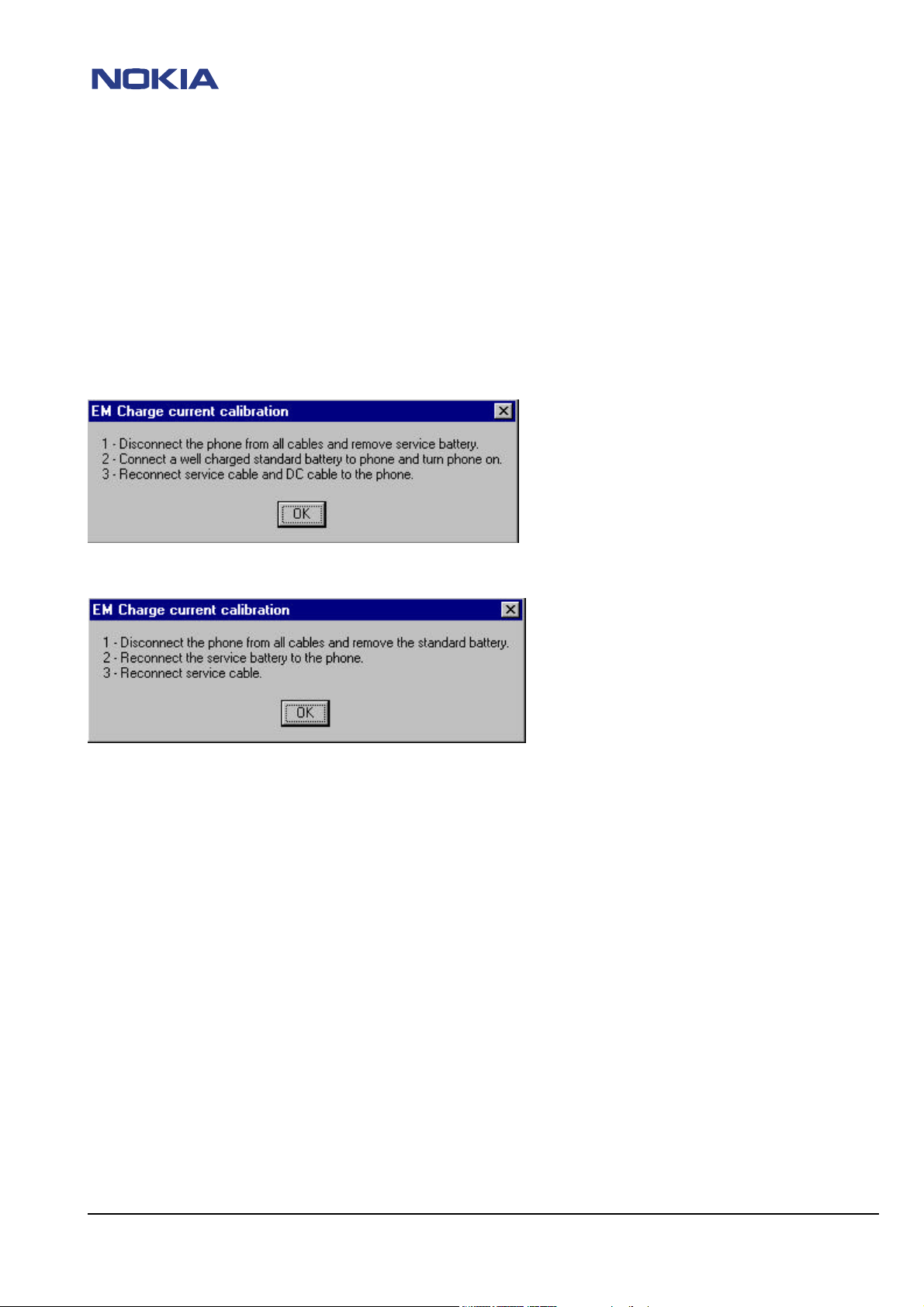
Energy management calibration information
If it is necessary to realign, it is imperative to follow the instructions displayed in the pop-up windows!
As soon as you take an other order as given from WinTesla, the alignment will be failed or will stop and you must begin once
more.
Follow these instructions as shown in pictures and your energy management calibration will work.
First step: (Charge current)
Second step: (Charge current)
If all of the measurements are OK, the values are now adjusted.
If one or more values failed, see charging problems on page #14.
© 2001 NMP
Checked by:
CC Training Group
Approved by:
SACE
Page 6
CONFIDENTIAL
6 (29)
HDa-13/S 893 Repairhints
Service & Analysis Center Europe Introduction Version 1.2 Approved
SACE CC Training Group Date 2001-03-16
TX tuning
Has to be tuned in both bands, but only on middle channels :
CH38 – 897,6 MHz for EGSM and CH700 – 1747,8 MHz for PCN.
TX I/Q tuning has to be done for both bands.
Reference are always target- values given from WINTESLA.
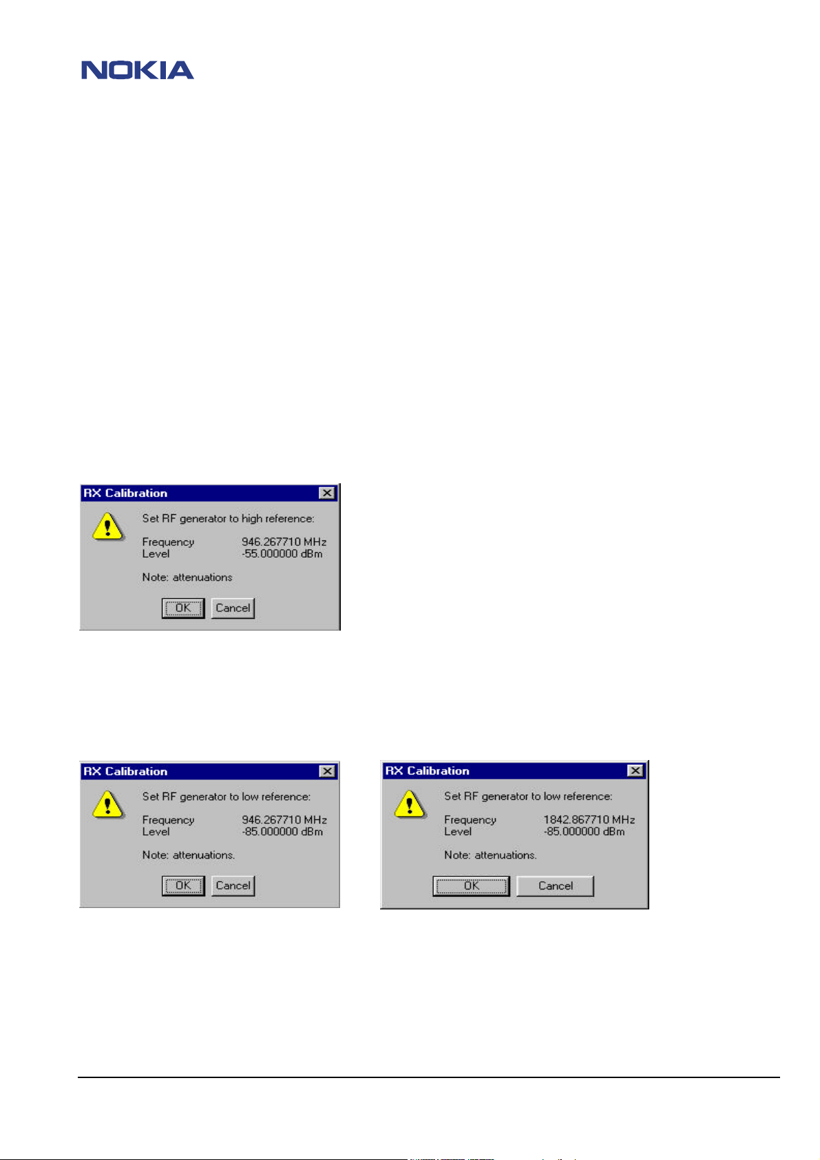
RX calibration
RSSI (Radio / Received Signal Strength Indicator)
The "RX calibration" is used to determine gain at different gain-settings for front-end and Hagar and needs to be done in both
bands, but the calibration only has to be started once, it will automatically proceed to the PCN band after EGSM.
Note: If the frequency in your Wintesla is different from 946.2671 MHz ,you will have to close Wintesla and add or edit
these lines in your tesla.ini file:
[NPE-3_TUNING]
RXChannelGSM =56
TXChannelGSM =38
Restart Wintesla and redo RX Calibration.
Note if the low level in your Wintesla is different from –85dBm, you will have to close Wintesla and add these lines in your
tesla.ini file:
[NPE-3LEVELS]
RSSILow =-85
RSSIHigh =-55
Restart Wintesla and redo RX Calibration
Note : Check if AGC-values are in ascending order (10dBm/step, exception: In PCN mode gainstep 2 to 3 is only ~5dBm)
© 2001 NMP
Checked by:
CC Training Group
Approved by:
SACE
Page 7
CONFIDENTIAL
7 (29)
HDa-13/S 893 Repairhints
Service & Analysis Center Europe Introduction Version 1.2 Approved
SACE CC Training Group Date 2001-03-16
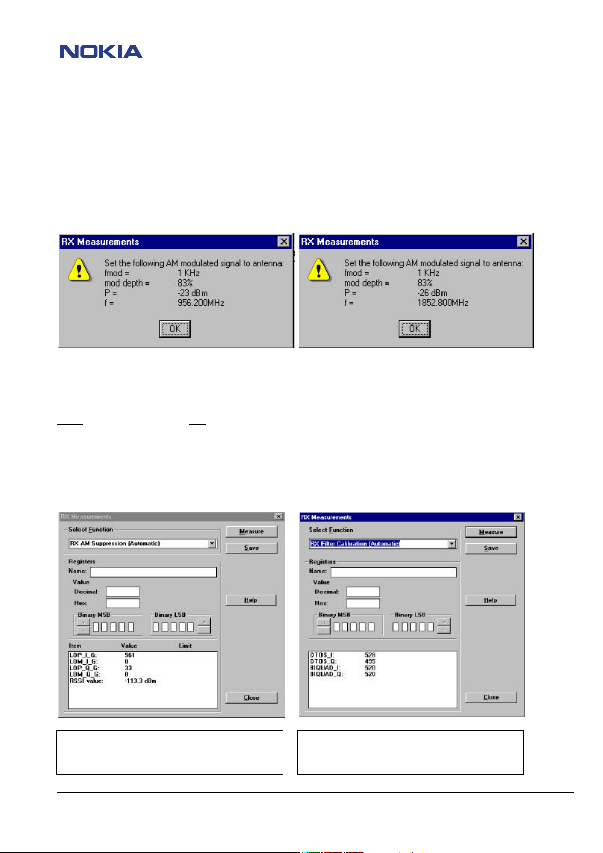
AM suppression tuning
Tune's four Hagar internal resistors of RX demodulator.
Purpose is to minimize the effect of any kind of AM interference to RX performance.
Tuning is automatic but it needs AM-modulated signal to phones` antenna input and has to be done for both bands.
NOTE:
Set the generator to the level or frequency shown in your wintesla window!
NOTE : WINTESLA WILL USE CH.56/700+10MHz INSTEAD OF ALL MANUAL SETTINGS IN TESLA.INI !
Use these settings:
EGSM PCN
Fmod=1kHz Fmod=1kHz
Mod depth=83% Mod depth=83%
P=-23dBm P=-26dBm
F=956.2MHz F=1852.800MHz
AM supression results should be in a range for:
EGSM –86dBm to –130dBm, PCN -95dBm to
–130dBm
© 2001 NMP
Checked by:
RX filter calibration results for AD values should be
in a range between 0 and 1023.
CC Training Group
Approved by:
SACE
Page 8

CONFIDENTIAL
8 (29)
HDa-13/S 893 Repairhints
Service & Analysis Center Europe Introduction Version 1.2 Approved
SACE CC Training Group Date 2001-03-16
Description of Signals & Voltages
The cause of this list are some new named signals/voltages in opposite to former names which are used in this document
(where to measure) & for a better understanding in addition to the service manual.
Startup sequence/CCONT section
PWRON/WDDISX (J102/R401) Always high level, only pulled down as long as powerkey is pressed.
PURX (J101) Power-Up-Reset signal from CCONT. When the voltages are stable, this line is on high level
allowing the MAD to run (Masterreset).
CCONTCSX (J100) Chip select for the CCONT. Used when the MAD wants to access the CCONT on the serial
bus (the serial bus is shared with the display) GENSIO-bus.
CCONTINT Interrupt from the CCONT to the MAD; for example: from the Real Time Clock, when a
charger is connected or when an intelligent battery powers the phone up
CHARG_CTRL (J114/C171) Output to the charger, when using 3-wire charging. The duty cycle of this 32Hz signal
switches the output current of the ACP-9 charger.
RFC (J601) Reference Frequency Clock. High stability clock signal for the digital circuits inBaseband
(13MHz)
SLEEPCLK (J112/C113) 32kHz clock generated in CCONT RTC. Used by MAD during sleepmode
SYNTHPWR (J317) Control line from MAD to CCONT. Turns on/off 3 voltage regulators for RF
VCXOPWR/SLEEPX (J331/J333/R305) Control line from MAD to CCONT. Controls the sleep-mode by turning on/off regulators
needed during normal/sleep
VB (J103/C105) Battery voltage
VCORE (C155) Digital baseband supply for the MAD core, 1.7 –1.9V
VBB (J108/C147) Digital baseband supply, 2.7V
VCOBBA (J109/C254) Analog baseband supply, 2.7V (used for audio)
VBATTIR (L121) Battery voltage for supplying IRDA, VIBRA and BUZZER
VBATTRF (L122) Battery voltage for the Power amplifiers (RF)
VBATTUI (L120) Battery voltage for supplying LED’s
VREF (J117/C143) 1.5V reference voltage (+-1,5%) generated by CCONT
VREF_RX (R510) Reference voltage for HAGAR, generated by COBBA
VSYN_1 (J106/C130) Supply voltage for SHF VCO
VSYN_2 (C133) Supply voltage for digital and analog circuits in HAGAR (VLO,VPRE,VBB, VF_RX)
VRX (J104/C136) Supply voltage for HAGAR part of the RX chain
VTX (J107/C142) Supply voltage for the TX chain in HAGAR
VXO (J105/C141) Supply voltage for the VCTCXO and VDIG in HAGAR
VCP (J110/C157) 4,9V supply voltage for PLL charge pump HAGAR
V_IN (F101) Charger input
VPP (C349) 12V input for fast flashing. In normal use, this line of the Flash is used for write protecting
the flash, and is then controlled by MAD with a possible overrule from a voltage detection
circuit. So if the battery is removed, the voltage detector disabled writing to the flash
VIRDA (C139) Regulator (2.7V), that turns the Infrared device and buffers on/off
RAM_BCK (C135) Backup-supply to SRAM. When the phone is turned off, the SRAM gets power from the
RTC-battery, so that data is not lost
BATTIO (V120) Signal used for turning ON an intelligent battery from the phone
© 2001 NMP
Checked by:
CC Training Group
Approved by:
SACE
Page 9
CONFIDENTIAL
9 (29)
HDa-13/S 893 Repairhints
Service & Analysis Center Europe Introduction Version 1.2 Approved
SACE CC Training Group Date 2001-03-16
RF part
AFC (R604) Automatic Frequency Control - analog control signal for 26 MHz VCTCXO fine tuning
COBBACLK (J200) 13MHz clock from MAD to COBBA - used for syncronized serial communication between
COBBA and MAD
HAGARRESET (J500/N501) Reset signal from MAD to HAGAR
DET (V800) Detector signal between powerdetector and HAGAR
SCLK (J502/J506) Clock for HAGAR serial programming (26 MHz)
SDATA (J503/J507) Data for HAGAR serial programming
SLE (J501/J505) Serial Latch Enable for HAGAR serial programming (formerly titled as SENA)
RXI, RXQ (R509) The RX baseband signals (after downconversion)
GSM_RX (Z700) EGSM RX signal between RX/TX switch and 1st EGSM SAW
GSM_TX (L800) EGSM TX signal between dual-coupler and RX/TX switch
TXP (R512) Transmitter power enable - used for timing of the power loop, Enables the operation
amplifier in HAGAR
TXC (R518) Transmitter power control signal, that controls the level of the output power and the shape
of the burst
VPCTRL_G (V803) Control line for PA output power
TXVDET (C531) Supply voltage for the RF power detector circuit
TXBUF_G (C807) Supply voltage for EGSM TX buffer
TXBUF_P (C829) Supply voltage for PCN TX buffer
LNA_G (C706) EGSM LNA supply voltage, front-end gain on/off
LNA_P (C700) PCN LNA supply voltage, front-end gain on/off
LNAB_G (R708) BIAS for both LNA’s, front-end gain on/off
TXI_0, TXI_180 (R513) Differential In-phase TX signals to the IQ-modulator
TXQ_0, TXQ_180 (R516) Differential quadrature-phase TX signals to the IQ-modulator
TXVGSM (R910/N800) Selects GSM Tx mode in PA and RX/TX Switch
TXVPCN (R911/N800) Selects PCN Tx mode in PA and RX/TX Switch
OUTM_G_TX (L802) Balanced EGSM TX signal between HAGAR and EGSM TX balun
OUTP_G_TX (L802) Balanced EGSM TX signal between HAGAR and EGSM TX balun
OUTM_P_TX (L804) Balanced PCN TX signal between HAGAR and PCN TX balun
OUTP_P_TX (L804) Balanced PCN TX signal between HAGAR and PCN TX balun
INM_GSM_RX (L704) Balanced EGSM RX signal between EGSM RX balun and RF input of HAGAR
INP_GSM_RX (L704) Balanced EGSM RX signal between EGSM RX balun and RF input of HAGAR
INM_LO (T600) Balanced VCO signal between VCO balun and VCO input of HAGAR
INP_LO (T600) Balanced VCO signal between VCO balun and VCO input of HAGAR
INP_PCN_RX (L703) Balanced PCN RX signal between PCN RX balun and RF input of HAGAR
INM_PCN_RX (L703) Balanced PCN RX signal between PCN RX balun and RF input of HAGAR
OSC_DIV/TOUT (C614) Reference divider output (13 MHz) -- RFClock
OSC_IN (G602) Reference frequency input from ref oscillator
OUT_CP (C605) Output of the PLL charge pump
PCS_RX (Z701) PCN RX signal between RX/TX switch and 1st PCN SAW
PCS_TX (L800) PCN TX signal between dual-coupler and RX/TX switch
© 2001 NMP
Checked by:
CC Training Group
Approved by:
SACE
Page 10

CONFIDENTIAL
10 (29)
HDa-13/S 893 Repairhints
Service & Analysis Center Europe Introduction Version 1.2 Approved
SACE CC Training Group Date 2001-03-16
Digital/programming part
MBUS (J113/R172) Bidirectional serial bus between MAD and accessory - during flashing, clock signal is
received on this line
MBUS1 (V170) Same as above, but on the “dirty” side of the filter
FBUS(1:0) (V171) FastBus. Consisting of FBUS_RX and FBUS_TX signals. Used for IRDA and accessory
communication. During flashing, the data is transferred on these lines
FBUS_RX(J332/R306) Receive line from the MAD’s point of view
FBUS_TX(J331/R305) Transmit line from the MAD’s point of view
User Interface part
XEAR (L201) Audio output when using carkit or headset
XMIC (L201) Audio input when using carkit or headset
MICN (L200) Negative side of the microphone
MICP (L200) Positive side of the microphone
PD2 (R201) Signal for muting microphone in headset, controlled by MAD
BUZZER (R410) PWM-signal from MAD, controls the buzzer
LCDCD (J328) Signal for controlling if the display is to receive data or control information on the serial
bus
LCDEN (J451) Chip enable signal to the display, informing that data on the serial bus is to the display
driver
LCDRSTX(R430) Reset signal from MAD to display driver
LIGHT (R427) Signal from MAD, that turns on the LED’s for keyboard and backlight
ROW(4:0) (V450) Keyboard matrix scan lines
COL(4:0) (V450) Keyboard matrix scan lines
CARDDET (C127) Used for detecting removal of the battery. When the battery is removed, this signal goes
high before the power is lost, giving the MAD time to power down the SIM-card
SIMIF(4:0) (J300) Serial bus for transferring SIM-data between MAD and CCONT
HEADDET (C211) Used for detection of which accessory has been connected to the system connector by
measuring the voltage on XMIC. Connected to A/D-converter in CCONT, and I/O-pin on
MAD. Data can also be transferred, for example - between MAD and DLR3-cable
HOOKDET (C212) For detecting when the push-button on the headset is pressed
DLR3 (V221) When the DLR3-cable is detected, this signal controls a switch, which gives power to the
cable
SGND (L201) Return line for microphone and earpice when a headset is connected to the phone. When
the DLR3-cable is connected, it changes to a power supply line to the cable, supplying 2.7V
© 2001 NMP
Checked by:
CC Training Group
Approved by:
SACE
Page 11

CONFIDENTIAL
11 (29)
HDa-13/S 893 Repairhints
Service & Analysis Center Europe Introduction Version 1.2 Approved
SACE CC Training Group Date 2001-03-16
USER INTERFACE FAILURES
Display failure
Check mechanical appearance of H400 and C451.
Check contact pads on PCB – clean also if necessary
Check VBB 2,7V at C452
Check if Vout 7,6V / 70mVpp at C451 (noise < 100mV), if noise is higher, C451 may be broken.
Change LCD unit if failure persists - probably MAD D301 faulty.
If the LCD shows too much contrast and / or LCD flickers, check if C451 is broken.
If there are vertical or horizontal lines missing, LCD unit electrical defect.
Keypad malfunktion
Check if domesheet contacts are dirty, clean PCB (keypads) if necessary
Check mechanical appearance of domesheet (LCD unit) itself.
Check resistance of ROW and COL lines between the keys (0 Ohm)
Change LCD unit.
If keypad is still malfunctioned - probably MAD D301 faulty.
If keypad crackles when pressing keys, change keypad.
Backlight failure
First check mechanical condition and position of baseband shield, check for shorts, etc.
Check VBATTUI 3,6V at L120
Check VBATTUI 3,6V at R424
Check voltage at V430 (LCD lights) 3,6V and at LED´s V420 – V423
Check voltage at V431 (Key lights) 3,6V and at LED´s V424 – V429
Check voltage at R427 (LIGHT line) – if this fails, MAD D301 or PCB faulty
Note: Different LEDs for LCD (brighter) and keypad backlight.
Clock time problems.
Clock time has to be corrected in short periods.
Check amplitude and frequency of sleepclock oscillator at J112 / C113 should be 3,2Vpp squarewave at 32,768kHz.
If not ok, change B110 and check parts around oscillator :(R110, R111, R112, R113, C110, C111, C112, C113).
Clock time is lost after removing battery.
First try to charge RTC battery, by connecting battery to the phone for app. 10 minutes.
If fault remains, check contact springs of battery or change RTC battery (LCD unit). Check VBACK 3.2V at RTC battery G100
If fault persists, probably CCONT N102 or CHAPS N100 faulty.
32 kHz before and after C113.
© 2001 NMP
Checked by:
CC Training Group
Approved by:
SACE
Page 12

CONFIDENTIAL
12 (29)
HDa-13/S 893 Repairhints
Service & Analysis Center Europe Introduction Version 1.2 Approved
SACE CC Training Group Date 2001-03-16
Vibra failure
Check mechanical appearance of M400
Check VBATTIR 3,6V at L121
Check VBATTIR 3,6V at V440
Check vibra signal at L401. If not ok check VIBRA signal at R444
If signal is ok at R444 change V441, if signal fails,
MAD D301 is probably faulty, or a disconnection between MAD and R444 in VIBRA line is the reason
Buzzer failure
Check mechanical condition of buzzer B400
Check VBATTIR 3,6V at L121
Check buzzer signal at R410
Check buzzer signal in and out at V410
Change buzzer B400 if all of the above works
© 2001 NMP
Checked by:
CC Training Group
Approved by:
SACE
Page 13

CONFIDENTIAL
13 (29)
HDa-13/S 893 Repairhints
Service & Analysis Center Europe Introduction Version 1.2 Approved
SACE CC Training Group Date 2001-03-16
SIMcard failures
SIMcard not accepted
Use Wintesla to open normal mode/quick/RF info window - compare shown SIMlock data with the listed entries of the respective
productcode (see SIMlock list).
If shown SIMlock data is the same as in the list – Status is ok und must be set so!
Probably MSIN data field is closed to special IMSI number range, it only can be opened by operator
(refer to general Service Bulletin 065).
If SIMlock data is not the same as in SIMlock list or somehow corrupted, SIMlock-data must be rewritten with the
Nokia-security password.
If SIMlock is corrected or inactive but fault remains - N240 is faulty, or there are probably broken solderings under COBBA change N240 - realign RX / TX values and rewrite SIMlock data and flash the phone after this again.
“Insert SIMcard“ appears in Display
Check X160, if bent or soiled - change if necessary
Check BSI A/D values (ok range 340-350)
Check V160: pin1 – DATA_0, pin3 - VSIM, pin4 - SIMCLK, pin5 – SIMRST_0
Check also R160, C160, C161, C162
Check resistance of SIMlines to GND - change V160, C163, C164 if necessary, probably broken solderings under CCONT N102
Change CCONT N102 and run energy management calibration, if fault persists - probably MAD D301 or PCB faulty.
SIMcard Signals
SIMCLK DATA_0
SIMRST_0 VSIM
© 2001 NMP
Checked by:
CC Training Group
Approved by:
SACE
Page 14

CONFIDENTIAL
14 (29)
HDa-13/S 893 Repairhints
Service & Analysis Center Europe Introduction Version 1.2 Approved
SACE CC Training Group Date 2001-03-16
CHARGING PROBLEMS
At first try an energy management calibration; either to define the defective area, or the phone works well after calibration.
(See page #5)
“NOT CHARGING“ appears on display
If calibration failed – check possible failure message:
Battery temperature failed: Check X120, X121, R122 / R123, R124, V120, change N102 if necessary.
Battery size failed: Check X121, X120, R120 / R121, change N102 if necessary.
Battery voltage failed: Check L123 / R105 / C104 / C105, change N102 if necessary
Charge current failed: Check R106, change N100 and / or N102.
Charge voltage failed: Check VCHARGE at voltage devider R102 / R103, if ok – change N102,
if not ok - check X001, R101, F101, L101, change N100 if necessary.
X120 / X121 battery connector, X001 system connector.
Check mechanical condition of connectors – change if necessary.
V_IN line short-circuited to GND
Check resistance of V_IN line at F101 to GND (50 kOhm), if resistance is not ok - remove L101 and check again.
If resistance is ok now - C101 / C102 or N100 should be the reason, if resistance is still not ok – R101 faulty.
CCONT / N102 faulty
Change CCONT N102 if any A/D (calibration) value, is out of limit and DC voltage is ok.
If DC voltages are not ok, check corresponding voltage dividers and battery connectors X120 / X121, always realign RX/TX and
AD values after changing CCONT N102.
Nothing happens if charger is connected
F101 faulty
Check resistance of F101 ( 0 Ohm ).
Check voltage at R103 > 0,4V if charger is connected. If not ok (<0,4V) – check / change X120,X121, F101, R101, R102/R103,
if ok - change N100 and / or N102.
Energy management calibration.
Calibration has to be done always if any part in charging circuit has been replaced.
Try calibration, if charging process stops too early or doesn´t start and if message “NOT CHARGING” appears on Display.
( Also see “General tuning informations“ )
© 2001 NMP
Checked by:
CC Training Group
Approved by:
SACE
Page 15

CONFIDENTIAL
15 (29)
HDa-13/S 893 Repairhints
Service & Analysis Center Europe Introduction Version 1.2 Approved
SACE CC Training Group Date 2001-03-16
CONTACT SERVICE
MCU Boot failure
Serial clockline failure
Serial Dataline failure
Connect WDDISX
(R401) to GND
Check Vbb 2.7V at J108/
C147
OK
Check
SLEEPX/VCXOPWR 2.7V
at J333 or J331
OK
Check VXO 2.7V at
J105/C141
OK
Check 13MHz
CLK frequency at C613
OK
Check resistance to GND
F/MBUS lines
J113/331/332
nOK
nOK
nOK
nOK
OK
Continue with section
"Phone does not
switch on"
D301 faulty, swap
Continue with section
"Phone does not
switch on"
Check values at G602,
V600
Check R172, V170, V171,
R305/306,X001
© 2001 NMP
OK
MAD or PCB faulty
OK
Checked by:
CC Training Group
Approved by:
SACE
Page 16

CONFIDENTIAL
16 (29)
HDa-13/S 893 Repairhints
Service & Analysis Center Europe Introduction Version 1.2 Approved
SACE CC Training Group Date 2001-03-16
CONTACT SERVICE PROBLEMS
This fault means that the phone software is able to run and thus the watchdog of CCONT N102 can be served. Selftest
functions run when power is switched on and program is executed from FLASH
If any selftest fails, - “CONTACT SERVICE” appears in Display.
Note: Always try SW-update to solve the problem or locate the error - in most of the cases phones are ok after update.
Possible failures:
MCU ROM Checksum failed :
Try to flash the phone. If not ok after flashing – change FLASH D311 if you are authorized to rewrite IMEI and SIMlock data,
if failure persists after changing D311, MAD D301 defect which is not changeable.
CCONT Interface failed :
Probably broken solderings under CCONT N102
If not ok after rework of CCONT, probably MAD D301 or PCB faulty. Run energy management calibration after changing CCONT!
NOTE: For Energy management calibration see also general tuning information page!
COBBA parallel/serial failed
Check VBB 2,7V at C147, VCOBBA 2,7V at C254 & COBBACLK at J200
If all ok – change COBBA N240
If the failure persists after changing COBBA – probably MAD D301 or PCB faulty.
DSP Alive failed
In most of all DSP alive selftest failures MAD D301 is faulty, which is not changeable.
EEPROM tune checksum / security checksum failed
Use Wintesla to check if phonedata like IMEI, product data or PSN are corrupted.
If phone data is ok, try to reset the phone. If phone data is not ok or fault remains after reset, FLASH D311 is faulty.
RTC Battery failed
First try to charge RTC battery by switching on the phone for app. 10 minutes
If fault remains, check contact springs of battery.
In some cases it is necessary to change CCONT N102.
© 2001 NMP
Checked by:
CC Training Group
Approved by:
SACE
Page 17

CONFIDENTIAL
17 (29)
HDa-13/S 893 Repairhints
Service & Analysis Center Europe Introduction Version 1.2 Approved
SACE CC Training Group Date 2001-03-16
PHONE DOES NOT SWITCH ON
First check always current consumption: off state 0-2,3mA, sleep mode 2,3-4mA.
If too high – see section „low standby / operation mode time“.
Disable watchdog if phone switches off after 2 or 3 seconds.
Check connectors X001/X120/X121 - change if bent or soiled.
Check VB 3,6V at J103/C105 - if not ok, check/change L123.
Check if PWRON at R401/J102 drops to 0V while pressing powerswitch, if not ok - check/change S402, R401.
Check 32,768kHz at J112/C113, 3Vpp squarewave – (if it is difficult to measure squarewave, because of Basebandshield,
check 32,768 kHz at the other side of C113, 900mVpp sinewave).
If not ok, check/change components around B110, (R110-R113 & C110-C113) and/or change CCONT N102 if necessary.
Check VCORE at C155 – 1,7V – if not ok, change CCONT N102.
Check VBB 2,7V at J108/C147, VXO 2,7V at J105/C141, VREF 1,5V (+-1,5%) at J117/C144 –if not ok, check resistance of lines
to GND and/or change CCONT N102 if necessary.
Check SLEEPX/VCXOPWR 2,7V at J333/J331 - if not ok, MAD is faulty in all probability - swap the phone, because MAD D301 is
not changeable.
Check PURX 2,7V at J101 after pressing powerswitch - if not ok, change CCONT N102.
Check 13MHz Clk frequency (RFC) at C613, if not ok, check values around 26MHz oscillator G602 / V600
Change HAGAR N500 if necessary.
Try to flash the phone - if not ok, see section “FLASH update not possible“.
Note:
It is nessesary to realign all RX/TX values after changing HAGAR N500 and run energy management calibration after changing
CCONT N102.
For Energy managemant calibration see also general tuning information page!
32,687 kHz before and after C613.
© 2001 NMP
Checked by:
CC Training Group
Approved by:
SACE
Page 18

CONFIDENTIAL
18 (29)
HDa-13/S 893 Repairhints
Service & Analysis Center Europe Introduction Version 1.2 Approved
SACE CC Training Group Date 2001-03-16
LOW STANDBY / OPERATION MODE TIME
Off state current > 0-2,3mA.
lift L122 (VBATTRF) - check current consumption, if ok - N800 faulty in all probability,
if current is still too high after changing N800. check / change C814, C815, C817.
Lift L123 (VB) - check current consumption – if too high,
VB line faulty
In most cases is CCONT N102 the reason. If fault persists after changing CCONT, it is also possible, that capacitor(s) in VB line
is/are faulty (C105, C122, C123, … ). Check all these components lifting one after the other, with repeated current testing.
If fault persists, probably one of the µBGA / CSP´s and / or PCB should be the reason.
Sleep mode current > 2,3-4mA
Check resistance of all voltage output lines of CCONT N102 to GND
Check component(s) in corresponding line(s) if resistance is not ok
If resistance of voltage lines (from CCONT N102) are ok, but sleep mode current is still too high – change CCONT N102.
Check charging circuit, run energy management calibration.
If calibration fails - continue with section “Not charging“
Align RX / TX values. If calibration fails - continue with section “RX / TX faults”.
Note:
Standby time also depends on network side and users handling, like lights on/off, VIBRA- / WAP activities, games etc.
FLASH UPDATE NOT POSSIBLE
Check if fault code from prommer is one of the following:
MCU boot failure, serial clock/data line failure:
Connect „watchdog disable“ WDDISX R401 to GND.
Check VBB 2,7V at J108/C147 and VXO 2,7V at J105 / C141, if not ok - continue with section “PHONE DOES NOT SWITCH ON“
Check SLEEPX 2,7V at J333 - if not ok - MAD D301 faulty in all probability
Check PURX 2,7V at J101 - if not ok change CCONT N102
Check 13MHz Clk frequency at C613, approximately 800mVpp, if not ok, check values around 26MHz oscillator G602 / V600,
change HAGAR N500 if necessary
Check resistance of MBUS / FBUS lines (J113 / J331 / J332) to GND, also check R172, V170, V171,R305, R306 and check
X001.
If update still not possible – swap the phone, MAD D301 or PCB should be the reason.
Algorithm code fail, alias ID missing:
Update FPS4 box with the latest flash device list and try to update again, if fault remains, check values at MAD D301.
If ok, change FLASH D311
External RAM failure:
Check values at MAD D301, if ok - SRAM D310 faulty and/or change FLASH D311 if necessary.
See chapter “PHONE DOES NOT SWITCH ON”
Note:
It is necessary to run energy management calibration after changing CCONT N102!
For Energy managemant calibration see also general tuning information page (#5).
© 2001 NMP
Checked by:
CC Training Group
Approved by:
SACE
Page 19

CONFIDENTIAL
19 (29)
HDa-13/S 893 Repairhints
Service & Analysis Center Europe Introduction Version 1.2 Approved
SACE CC Training Group Date 2001-03-16
NO SERVICE PROBLEMS
No RX EGSM
Use Wintesla to set phone in following mode: Initialise / Local mode / Testing / RF Controls / Gain step value >2 / active unit RXburstmode / Channel 56 (946,2MHz). Set Generator to same frequency, -40dBm.
Check 26MHz reference oscillator frequency at G602, 800mVpp/frequency deviation < 100Hz
Check 946,2MHz at C912, if not ok, check/ change Z900, X900.
Check 946,2MHz at L700, if not ok, check/change Z700.
Check 946,2MHz at V700 in & out, if not ok, check LNA values: VLNAB_G 2,7V at V700, pin 8 and LNA_G 0,7V at pin4, change
HAGAR N500 if necessary.
Check 946,2 MHz at L704 - if not ok, check/change Z703, R702, T700.
Check RXIQ signals at R509, if not ok, check supply values at HAGAR N500: 2,7V at C513 (VXO), C501 (VRX), C503(VSYN_2)
and N501 input 4,9V (VCP). If one or more of these fails, change N102.
Check SDATA at J503/J507, SCLK at J502/J506 and SLE at J501/J505, if not ok MAD D301 faulty
Check VREF (1,5V) at R514 / VREF_RX (1,2V) at R510, if not ok, change N102.
Check frequency of SHF oscillator G600 if possible – refer to EGSM frequencies list.
If all values are ok but no RXIQ signals measurable at R509, HAGAR faulty, or there are probably broken solderings under N500.
If signals at R509 ok, but still no RX calibration possible, check values at COBBA N240:
VBB at C256 (2,7V) and VCOBBA at R245 (2,7V), also check COBBACLK at J200.
If values ok – N240 faulty, or there are probably broken solderings under COBBA.
No RX PCN
Use Wintesla to set phone in following mode: Initialise / Local mode / Testing / RF Controls / Gain step value >2 / active unit RX
burst / Channel 700 (1842,8MHz). Set Generator to same frequency, -40dBm.
Check 26MHz reference oscillator frequency at G602, 800mVpp/frequency deviation < 100Hz
Check 1842,8MHz at X900 and ANT pad of Z900 - change X900 if necessary.
Check 1842,8MHz at C913, if not ok, check solderings of Z900, change if necessary .
Check 1842,8MHz (PCS_RX) at C702 - if not ok, check/change Z701.
Check 1842,8MHz at C712 - if not ok check values of LNA: VLNAB_G = 2,7V at V701, pin 8 (VC) and LNA_P = 0,7V at pin 4 (VCC)
Change V701 if necessary.
Check 1842,8MHz at L703, If not ok, check/change Z702, T701
Check RXIQ signal at R509 - if not ok, check values at HAGAR N500: 2,7V at C513 (VXO), C501 (VRX), C503 (VSYN_2) and
N501 input 4.9V (VCP).
If one or more of these fails - change N102
Check SDATA at J503/J507, SCLK at J502/J506 and SLE at J501/J505, if not ok MAD D301 faulty.
Check VREF (1,5V) at R514 / VREF_RX (1,2V) at R510, if not ok, change N102.
Check frequency of SHF oscillator G600 if possible – refer to EGSM frequencies list.
If there is no possibility to check frequency - check if oscillator works by measuring VCC at C601 (2,7V) and VC at C603, which
varies between 0,7V and 3,8V (see EGSM list).
If VC is 4,8V, the oscillator doesn’t work in all probability, also check T600 and R608.
If all values are ok but no RXIQ signal is measurable at R509, N500 is faulty, or there are probably broken
solderings under HAGAR.
If signal at R509 ok but still no RX calibration possible, check values at COBBA N240: VBB 2,7V at C256 and VCOBBA 2,7V at
R245, also check COBBACLK at J200.
If values are ok, N240 faulty, or there are probably broken solderings under COBBA.
Note: After changing COBBA, HAGAR and/or CCONT it is necessary to realign all RX,TX -and AD values,
and rewrite IMEI and SIMlock data (COBBACHANGE)
© 2001 NMP
Checked by:
CC Training Group
Approved by:
SACE
Page 20

CONFIDENTIAL
20 (29)
HDa-13/S 893 Repairhints
Service & Analysis Center Europe Introduction Version 1.2 Approved
SACE CC Training Group Date 2001-03-16
NO SERVICE PROBLEMS
EGSM/PCN no RX
Change Z700
First check 26 MHz at G602 (700mVpp,+/-100Hz) Check SHF (list) and/or VC/VCC 2.7V (C601)
No service
(GSM900)
Check 946,2MHz at
Z900 (antennapad)
Check 946,2MHz at
C912
OK
Check 946,2MHz at
L700
OK
Check 946,2MHz at
V700
nOK nOK
OK
nOK nOK
nOK nOK
0.7-3.8V
Check/change X900
Check/change Z900
Check
LNAB_G at V700/701, VC (2.7V)
at pin8, 2,7V at pin4.
LNA_G = 0.7V
LNA_P =0.7V
No service
(GSM 1800)
Check 1842,8 MHz at
Z900 (antennapad)
Check 1842,8MHz at
Check 1842,8MHz at
Check 1842,8MHz at
C913
C702
C712
OK
OK
nOKnOK
OK
Change Z701
Check/change Z703,
R702, T700
© 2001 NMP
OK
Change
V700/701
Check 946,2MHz at
nOK nOK
L704
OK
Check RX IQ at R509 Check RX I/Q at R509
Check VBB 2.7V at C256, R245,
VCOBBA (2,7V) and COBBACLK at
Change N500
Check supply voltages
at N500: C513 (VXO);
C501 (VRX);
C503 (VSYN_L)
At N501: (VCP) 4.8V
Check
SDATA J503
SLE J501
SCLK J502
J200
nOKOK
Change N500
nOKnOK
Swap PCBChange N240
OK
Check 1842,8MHz at
L703
OK
Checked by:
CC Training Group
Check/change Z702
T701
Approved by:
SACE
Page 21

CONFIDENTIAL
21 (29)
HDa-13/S 893 Repairhints
Service & Analysis Center Europe Introduction Version 1.2 Approved
SACE CC Training Group Date 2001-03-16
NO SERVICE PROBLEMS / TX POWER
First of all: Try to calibrate RX / TX values to define the fault area, or phone works well after calibration
No or low TX power EGSM
Use Wintesla to set phone in following mode: Initialise / Local mode / Testing /RF Controls / active unit TX / Channel 38
(897,6MHz).
Check 26MHz reference oscillator frequency at G602 (800mVpp, frequency deviation < 100Hz)
CheckTXBUF_G at C807 – 2,7Vpp squarewave - see signal page #27
Check TXIQ signals at C525 / C526, refer to signals shown on page #27.
If not ok, check values at COBBA N240 (see COBBA N240 chapter page #24).
Check 897,6 MHz at T800 pin 4 and 6. If not ok, check signals at HAGAR N500 (see HAGAR N500 chapter)
Check 897,6 MHz at N800 pin 8. If not ok,check / change parts like T800,V801, Z802, Z800.
Check 897,6 MHz at L800 pin 1. If not ok, check values at N800.
Check 897,6 MHz at X902 (Antenna pad). If not ok, check / change X900.
Check L800 in & out, check also signal at Z900 in & out and TXVGSM: 2,7Vpp squarewave at C910 (sets Z900 into TX-mode).
No or low Tx power PCN
Use Wintesla to set phone in following mode: Initialise / Local mode / Testing /RF Controls / active unit TX / Channel 700
(1747,8MHz).
Check 26MHz reference oscillator frequency at G602 (800mVpp, frequency deviation < 100Hz).
Check TXBUF_P at C829 – 2,7V squarewave – see signal page #27
Check TXIQ signals at C525 / C526, refer to signals shown on page #27.
If not ok check values at COBBA N240 (see COBBA N240 chapter, page #24)
Check 1747,8MHz at T840 pin 4 and 6. If not ok check signals at HAGAR N500 (see HAGAR N500 chapter).
Check 1747,8MHz at N800 pin 8. If not ok check / change parts like T840,V802, Z800.
Check 1747,8MHz at L800 pin 2. If not ok, check values at N800.
Check 1747,8MHz at X902 (Antenna pad). If not ok, check / change X900.
Check L800 in & out, check also signal at Z900 in & out and TXVPCN: 2,7Vpp squarewave at C911 (sets Z900 into TX-mode).
© 2001 NMP
Checked by:
CC Training Group
Approved by:
SACE
Page 22

CONFIDENTIAL
22 (29)
HDa-13/S 893 Repairhints
Service & Analysis Center Europe Introduction Version 1.2 Approved
SACE CC Training Group Date 2001-03-16
NO TX
Check 26 Mhz at G602-
No TX
Check
CH38/897.6MHz at
OK OK
T800, pin 4/6
nOK nOK
Change N240
700mVpp/+/- 100hz, check SHF,
check Vbatt RF at L122
Check TX I/Q signals
nOK
Check TXC at C529
at R513/516
nOK
Change N240
Check
SDATA at J503
SLE at J501
SCLK at J502
If not OK, swap
OK
Check
OKOK
CH700/1747.8 MHz
at T840, pin 4/6
Change N102
Check 897.6MHz at
N800, pin8
OK
Check 897.6MHz
at L800, pin1
OK
Check 897.6MHz at
antennapad Z900
OK
Check 897.6MHz
at X902
nOK
nOK
nOK
nOK nOK
nOK
nOK
Check TXP at C524
Check/change
T840/Z800/V801
Check/change
T800/Z802/Z800/V801
N800 3.6V VBATT_RF, pin3,6
TXV_PCN 2.7Vpp sqw., pin 1
TXV_GSM 2.7Vpp sqw., pin 2
Vpc 1-1.6Vpp sqw.pin 7
Check/change
L800/Z900
Change X900
OK
nOK
nOK
nOK
Change N500
Check 1747,8MHz
at N800, Pin8
OK
Check 1747.8MHz at
L800, pin2
OK
Check 1747.8MHz at
antennapad Z900
OK
Check 1747.8 at X902
© 2001 NMP
Checked by:
CC Training Group
Approved by:
SACE
Page 23

CONFIDENTIAL
23 (29)
HDa-13/S 893 Repairhints
Service & Analysis Center Europe Introduction Version 1.2 Approved
SACE CC Training Group Date 2001-03-16
SHF OSCILLATOR PROBLEMS
This causes problems in EGSM and PCN mode (RX/TX).
If the phone has no service because of too low TX power (eg. approximately 5dBm in the highest powerlevels) and / or there are
strange A/D values in the RSSI measurements – check (if possible) the SHF frequency with a spectrum analyzer
and /or the RX calibration A/D values (also see pictures below) if there might be something unusual like a cutted SHF oscillator
frequency amplitude and / or the gain readings in RX calibration are lower as normal, - approximately about values of 10 to 20.
If this is the case, check the periphery – capacitors of SHF Oscillator G602 in VC circuit (C603, C604, C605)
Check their resistance to GND (approximately 3MOhm at R612 to GND in normal case / otherwise the value should be in lower
kOhm range (around 10k):
Left picture shows a normal SHF frequency amplitude – right side in defect case
Left picture shows normal gain readings – right picture in defect case (RX Calibration):
© 2001 NMP
Checked by:
CC Training Group
Approved by:
SACE
Page 24

CONFIDENTIAL
24 (29)
HDa-13/S 893 Repairhints
Service & Analysis Center Europe Introduction Version 1.2 Approved
SACE CC Training Group Date 2001-03-16
COBBA / N240 faulty
Check VBB 2,7V at C256 and VCOBBA 2,7V at R245
Check 13MHz COBBACLK at J200, probably broken solderings under COBBA / N240.
Realign Rx / Tx values after rework of COBBA N240.
HAGAR / N500 faulty
Check voltages at HAGAR:
VXO 2,7V at C533
VCP 4,7V at N501 (output)
VSYN_2 2,7V at C503
VRX 2,7V at C501
VREF 1,5V at C143
Check 26MHz reference oscillator frequency at G602:
800mVpp – frequency deviation < 100Hz.
Check TXIQ signals at R513/C525 (TXI 0/180) and R516 / C526 (TXQ 0/180)
Check SDATA at J503/J507, SCLK at J502/J506 and SLE (SENA) at J501/J505 (refer to signals shown on page #27)
Check TXC at C529 (diagram on page #25)
Check TXP at R512, 3Vpp squarewave/ 217Hz
Check frequency of SHF oscillator / G600 – refer to EGSM frequency list
If all values are ok but no TX - signal is measurable at T800, there are probably broken solderings under HAGAR, or N500 is
faulty.
Note: After changing COBBA, HAGAR and/or CCONT it is necessary to realign all RX,TX -and AD values,
and rewrite IMEI and SIMlock data (COBBACHANGE)
© 2001 NMP
Checked by:
CC Training Group
Approved by:
SACE
Page 25

CONFIDENTIAL
25 (29)
HDa-13/S 893 Repairhints
Service & Analysis Center Europe Introduction Version 1.2 Approved
SACE CC Training Group Date 2001-03-16
SIGNAL CHARTS
Serial data (RX Burst mode) Serial clock (RX Burst mode)
Serial Latch enable (RX Burst mode) TX power control TXC
TX power enable TXP TX_IN phase /Quadrature phase (0/180°)
© 2001 NMP
Checked by:
CC Training Group
Approved by:
SACE
Page 26

38
60
3
0
CONFIDENTIAL
26 (29)
HDa-13/S 893 Repairhints
Service & Analysis Center Europe Introduction Version 1.2 Approved
SACE CC Training Group Date 2001-03-16
FREQUENCY LIST
Channel TX RX VCO - TX VCO VCO - RX VCO
MHz MHz MHz VOLT MHz VOLT
1
124
512
700
885
890,2
897,6
902
914,8
1710,2
1747,8
1784,8
935,2
942,6
947
959,8
1805,2
1842,8
1879,8
3560,8
3608
3659,2
3420,4
3495,6
3569,6
VC at C603
1,7
2,01
2,34
0,84
1,3
1,77
3740,8
3788
3839,2
3610,4
3685,6
3759,6
VC at C603
2,81
3,2
2,03
2,36
2,66
975
976
977
978
979
980
981
982
983
984
985
986
987
988
989
990
991
992
993
994
995
996
997
998
999
1000
1001
1002
1003
1004
1005
1006
1007
1008
1009
1010
1011
1012
1013
1014
1015
1016
1017
1018
1019
1020
1021
1022
1023
880,2
880,4
880,6
880,8
881
881,2
881,4
881,6
881,8
882
882,2
882,4
882,6
882,8
883
883,2
883,4
883,6
883,8
884
884,2
884,4
884,6
884,8
885
885,2
885,4
885,6
885,8
886
886,2
886,4
886,6
886,8
887
887,2
887,4
887,6
887,8
888
888,2
888,4
888,6
888,8
889
889,2
889,4
889,6
889,8
890
925,2
925,4
925,6
925,8
926
926,2
926,4
926,6
926,8
927
927,2
927,4
927,6
927,8
928
928,2
928,4
928,6
928,8
929
929,2
929,4
929,6
929,8
930
930,2
930,4
930,6
930,8
931
931,2
931,4
931,6
931,8
932
932,2
932,4
932,6
932,8
933
933,2
933,4
933,6
933,8
934
934,2
934,4
934,6
934,8
935
3520,8
3521,6
3522,4
3523,2
3524
3524,8
3525,6
3526,4
3527,2
3528
3528,8
3529,6
3530,4
3531,2
3532
3532,8
3533,6
3534,4
3535,2
3536
3536,8
3537,6
3538,4
3539,2
3540
3540,8
3541,6
3542,4
3543,2
3544
3544,8
3545,6
3546,4
3547,2
3548
3548,8
3549,6
3550,4
3551,2
3552
3552,8
3553,6
3554,4
3555,2
3556
3556,8
3557,6
3558,4
3559,2
3560
1,46
1,51
1,56
1,61
1,66
1,7
3700,8
3701,6
3702,4
3703,2
3704
3704,8
3705,6
3706,4
3707,2
3708
3708,8
3709,6
3710,4
3711,2
3712
3712,8
3713,6
3714,4
3715,2
3716
3716,8
3717,6
3718,4
3719,2
3720
3720,8
3721,6
3722,4
3723,2
3724
3724,8
3725,6
3726,4
3727,2
3728
3728,8
3729,6
3730,4
3731,2
3732
3732,8
3733,6
3734,4
3735,2
3736
3736,8
3737,6
3738,4
3739,2
3740
2,66
2,69
2,72
2,75
2,78
2,81
© 2001 NMP
Checked by:
CC Training Group
Approved by:
SACE
Page 27

CONFIDENTIAL
27 (29)
HDa-13/S 893 Repairhints
Service & Analysis Center Europe Introduction Version 1.2 Approved
SACE CC Training Group Date 2001-03-16
Special information for NHM-3
This phone is build so that it can withstand a fall of 3 metres height without harmful effects – what certainly
does not mean that you should test this feature on purpose.
Further more the phone endures drops into water of 0.5metres depth up to 1minute at a water temperature of not
more than 50°C. Therefore the speaker, buzzer and microphone are sealed. Take care not to destroy these seals if you have
to change one of the above mentioned item, don´t even touch the seals!
To ensure water resistance, covers with gaskets must not be used more than three times after tightening the screws.
Check always appearance of gasket around systemconnector and battery cover, change parts in case of doubt!
It is absolutly necessary to use always new screws to assemble the phone, because gaskets around screws are surely
damaged after tightening them! Order / torque of tightening screws: middle screws at 12Ncm, top screws at 25Ncm and
then bottom screws at a torque of 25Ncm.
Note that accessories do not fulfill the same tough specifications as the phone is made for.
Do not connect any electrical item ( eg. charger, carkit ) to the phone if it is still damp!
The usage of NPE-3 Repair-Hints for NHM-3 phones is possible without any problems.
Schematics of both phones differ only in few points ( eg. varistors in Xmic-line, some more components around LNA… ),
and almost all itemcodes are the same.
Because of different systemmodul-forms you have to use MJS-23 Jig with XRC-3 Rf-cable for testing and adjustment.
If you have to make energy management calibration ( eg. after changing Ccont or any part of the charging circuit ), be
sure that you are using dll 311.04.00 or later, else the tuning of battery size won´t work and you will get the following
failure message:
One of the most conspicuous differences between NPE-3 and NHM-3 is the systemconnector, which is connected via
flexfoil to Pcb. Further more a batteryconnector similar to the one in NSM-2/3 is used. The Simcard-holder is combined
with the shielding of the baseband as well as the antenna is one part with the shielding of the poweramplifier. The RFconnector is constructed flexible, so that a fall does not result in torn off traces.
If it is necessary to change any item with help of a soldering machine ( eg µBGA-components, shieldings, poweramplifier…),
you have to remove the display assy first, which is connected to PCB with a flexfoil. This can be done easily with help of a
Metcal Soldering Station MX500 equipped with a soldering tip SMTC 162.
Hot air should not be used to desolder anything ever since using Pcb with microvias, which will crack rapidly if exposed to
too high temperature!
© 2001 NMP
Checked by:
CC Training Group
Approved by:
SACE
Page 28

CONFIDENTIAL
28 (29)
HDa-13/S 893 Repairhints
Service & Analysis Center Europe Introduction Version 1.2 Approved
SACE CC Training Group Date 2001-03-16
To remove the flexfoil release clips of display assy first and turn it around, so that you have access to the soldering points
of the foil. Now you can desolder the flexfoil easily.
Before soldering a new display ( do not use the old one! ) clean careful the soldering points. Add few new solder to the pads
and enclose only a little bit of flux.
Bend the flexfoil a little bit at the perforation, so that it is easier to hold the display in correct position. Do not touch the
contacts of the flexfoil with bare fingers!
Heat up the soldering points for approximately 10 seconds. Check connection visually ( especially at the top of the flex for
shorts to ground ) and clip display on Pcb. Never bend the flexfoil for more than 90°!
© 2001 NMP
Checked by:
CC Training Group
Approved by:
SACE
Page 29

CONFIDENTIAL
29 (29)
HDa-13/S 893 Repairhints
Service & Analysis Center Europe Introduction Version 1.2 Approved
SACE CC Training Group Date 2001-03-16
CHANGE HISTORY
Originator Status Version Date Comment
CC-TrainingGroup
CC-TrainingGroup
CC-TrainingGroup
Draft 0.1 24.01.2001 First draft version for the repair group
Approved
Approved
1.0 06.02.2001 First approved version
1.2 09.03.2001 Display information added
© 2001 NMP
Checked by:
CC Training Group
Approved by:
SACE
 Loading...