

Nokia 6200 Service Manual 07 npl3 sysmod

Customer Care Solutions
NPL-3 Series Transceivers
System Module and User
Interface
Issue 1 3/03 Company Confidential ãNokia Corporation

NPL-3 Company confidential
System Module and User Interface CCS Technical Documentation
Table of Contents
Page No
Glossary of Terms ..........................................................................................................3
Introduction ....................................................................................................................6
Electrical Modules .......................................................................................................6
Interconnection Diagram .............................................................................................6
System Module: Baseband .............................................................................................7
Baseband Module, technical summary ........................................................................7
Environmental Specifications ......................................................................................8
Temperature Conditions ............................................................................................8
Humidity and Water Resistance ................................................................................8
Baseband Technical Specifications .............................................................................9
Absolute Maximum Ratings ......................................................................................9
DC Characteristics .....................................................................................................9
Power Distribution diagram ....................................................................................11
Baseband External and Internal Signals and Connections ........................................12
FM Radio Interface .................................................................................................13
External Signals and Connections .............................................................................17
Keyboard (board-to-board) Connector ....................................................................17
LCD Connector (Board to Board) .............................................................................18
DC Connector ..........................................................................................................19
Bottom Connector ...................................................................................................19
SIM connector .........................................................................................................21
Internal Signals and Connections ............................................................................21
Baseband Functional Description ................................................................................23
Modes of Operation ...................................................................................................23
No Supply ................................................................................................................23
Back-up ...................................................................................................................23
Acting Dead .............................................................................................................23
Active ......................................................................................................................23
Sleep Mode ..............................................................................................................24
Charging ..................................................................................................................24
Battery .....................................................................................................................24
Power Up and Reset ...................................................................................................25
Power Up with PWR key ........................................................................................26
Power Up when Charger is connected ....................................................................26
Power Up when Battery is connected .....................................................................26
RTC Alarm Power Up .............................................................................................27
A/D Channels .............................................................................................................27
FM Radio ...................................................................................................................28
IR Module ...............................................................................................................28
SIM Interface ...........................................................................................................28
ACI ..........................................................................................................................29
External Accessory Regulator .................................................................................30
External Audio ...........................................................................................................30
External Microphone Connection ...........................................................................30
External Earphone Connections ..............................................................................31
Internal Audio ............................................................................................................32
IHF Speaker & Stereo Audio Amplifier .................................................................32
Page 2 ãNokia Corporation. Issue 1 3/03

Company confidential NPL-3
CCS Technical Documentation System Module and User Interface
Internal Microphone ................................................................................................32
Internal Speaker .......................................................................................................32
IHF Speaker & Stereo Audio Amplifier .................................................................33
Memory Block ...........................................................................................................34
Security ....................................................................................................................34
Clock distribution ......................................................................................................34
Audio Control ..........................................................................................................35
Accessory identification and Power Supply ............................................................35
Backup Battery ........................................................................................................36
RF Module Introduction ...............................................................................................37
RF Frequency Plan ....................................................................................................38
DC characteristics ......................................................................................................39
Regulators ................................................................................................................39
Typical current consumption ...................................................................................40
Power Distribution ..................................................................................................41
RF characteristics .........................................................................................................42
Channel Numbers and Frequencies .........................................................................42
Main RF characteristics ...........................................................................................42
Transmitter characteristics ......................................................................................42
Receiver characteristics ...........................................................................................43
RF Block Diagram ..................................................................................................43
RF Block Diagram NPL-3 .......................................................................................44
Frequency Synthesizers .............................................................................................45
Receiver .....................................................................................................................45
Transmitter .................................................................................................................45
Front End .................................................................................................................45
Power Amplifier ......................................................................................................46
RF ASIC Helgo .......................................................................................................47
AFC function ...........................................................................................................47
Antenna ..................................................................................................................47
User interface modules ..............................................................................................48
UI board WK4 .........................................................................................................48
Keyboard .................................................................................................................48
LCD .........................................................................................................................50
LCD & keypad illumination ....................................................................................51
Internal earpiece ......................................................................................................51
IHF ..........................................................................................................................51
Internal microphone ................................................................................................52
IR module ................................................................................................................52
Vibra ........................................................................................................................52
Pop-Port system connector ........................................................................................53
Issue 1 3/03 ãNokia Corporation. Page 3

NPL-3 Company confidential
System Module and User Interface CCS Technical Documentation
Glossary of Terms
ACI Accessory Control Interface
ADC Analog-Digital Converter
AFC Automatic Frequency Control
AGC Automatic Gain Control
API Application Programming Interface
ARM Processor architecture
ASIC Application Specific Integrated Circuit
BB Baseband
CBus Control Bus connecting UPP_WD2 with AEM and UEM
CCS Customer Care Solutions
CMT Cellular Mobile Telephone (MCU and DSP)
COG Chip On Glass
CPU Central Processing Unit
CTSI Clocking Timing Sleep Interrupt
CSP Chip Scale Package
CSTN Colour Super Twisted Nematic
DAC Digital-Analog Converter
DAI Digital Audio Interface
DB Dual band
DCT4 Digital Core Technology, 4th generation
DCN Offset Cancellation control signal
DLL Dynamic Link Library
DRC Dynamic Range Controller
DSP Digital Signal Processor
Page 4 ãNokia Corporation. Issue 1 3/03

Company confidential NPL-3
CCS Technical Documentation System Module and User Interface
EFR Enhanced Full Rate
EGPRS Enhanced General Packet Radio Service
EMC Electromagnetic compatibility
EMI Electromagnetic Interference
ESD Electro Static Discharge
EXT RF External RF
FBUS Asynchronous Full Duplex Serial Bus
GPRS General Packet Radio Service
GSM Global System for Mobile communications
HS Half Rate Speech
HSCSD High Speed Circuit Switched Data
IC Integrated Circuit
IHF Integrated Hands Free
IMEI International Mobile Equipment Identity
I/O Input/Output
IRDA Infra Red Association
LCD Liquid Crystal Display
LDO Low Drop-Out
LED Light Emitting Diode
LNA Low Noise Amplifier
MBUS 1-wire half duplex serial bus
MCU Micro Controller Unit
MDI MCU-DSP Interface
MFI Modulator and Filter Interface
Issue 1 3/03 ãNokia Corporation. Page 5

NPL-3 Company confidential
System Module and User Interface CCS Technical Documentation
PA Transmit Power Amplifier
PC Personal Computer
PCM Pulse Code Modulation
PCM SIO Synchronous serial bus for PCM audio transferring
PIFA Planar Inverted F-antenna
PWB Printed Wiring Board
PWM Pulse Width Modulation
RF Radio Frequency
RTC Real Time Clock
SIM Subscriber Identity Module
SW Software
UEM Universal Energy Management
UI User Interface
UPP Universal Phone Processor
VCXO Voltage Controlled Crystal Oscillator
VCTCXO Voltage Controlled Temperature Compensated Crystal Oscillator.
Page 6 ãNokia Corporation. Issue 1 3/03
Company confidential NPL-3
T
CCS Technical Documentation System Module and User Interface
Introduction
Electrical Modules
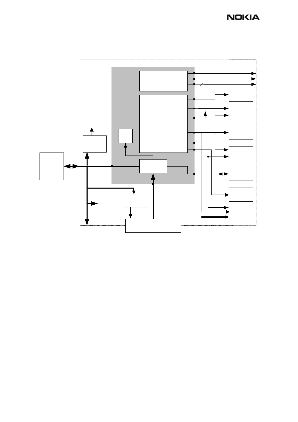
The system module WV8 consists of Radio Frequency (RF) and baseband (BB). User Interface (UI) contains display, keyboard, IR link, vibra, system connector and audio parts.
FM radio is located on the main PWB WV8.
The electrical part of the keyboard is located in separate UI PWB named WK4. WK4 is
connected to radio module PWB through a spring connector.
The Baseband blocks provide the MCU, DSP, external memory interface and digital control functions in the UPP ASIC. Power supply circuitry, charging, audio processing and RF
control hard ware are in the UEM ASIC.
The purpose of the RF block is to receive and demodulate the radio frequency signal from
the base station and to transmit a modulated RF signal to the base station.
The UI module is described in this section of the manual.
Interconnection Diagram
Keyboard
module
Antenna
Microphone
Figure 1: Interconnection diagram
Display
IHF
speaker
Radio
Module
NPL-3
NHL-4
IR Link
Earpiece
BatterySIM
Charger
omahawk
Accessories
Issue 1 3/03 ãNokia Corporation. Page 7
NPL-3 Company confidential
V
System Module and User Interface CCS Technical Documentation
System Module: Baseband
The System module (or Engine) consists of Baseband and RF sub-modules, each described
below.
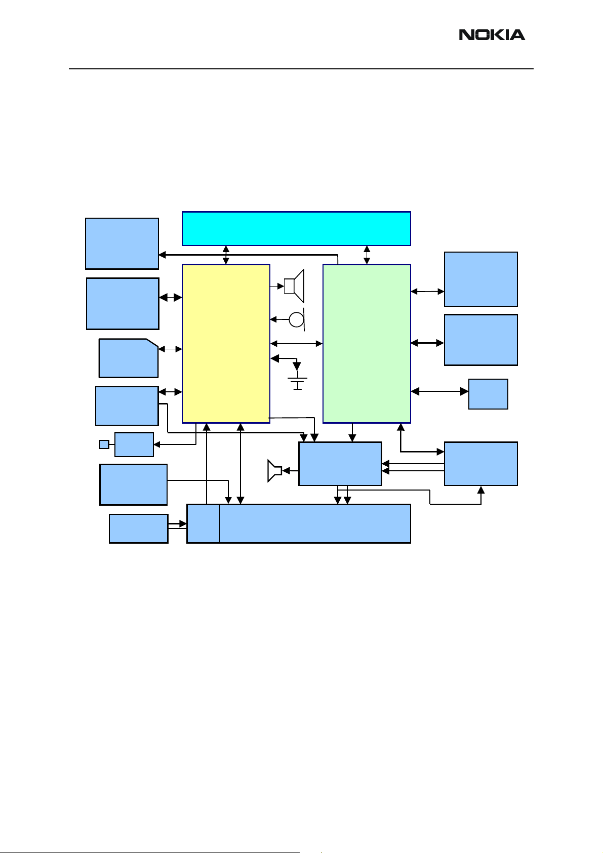
Baseband Module, technical summary
Main functionality of the baseband is implemented into two ASICs: UPP (Universal Phone
Processor) and UEM (Universal Energy Management).
LCD
Passive colour STN
4096 color
Led Driver
Keyboard &
display
illumination
SIM Reader
DCT-3
Battery
BLD-3
ibra
Accessory
Regulator
2.8V 70mA
Charger
RF Interface
UEMK UPP8Mv3
RTC
battery
Mo/St Amp
LM4855
Pop-Port
DC
jack
IHF
System connector
Combo
Memory
DCT-4 Flash 64Mbit
SRAM 4Mbit
Keyboard
IR
1.8V
FM radio
TEA5767
Figure 2: Baseband block diagram
Baseband is running from power rails 2.8V analog voltage and 1.8V I/O voltage. UPP core
voltages can be lowered down to 1.0V, 1.3V and 1.5V. UEM includes 6 linear LDO (Low
Drop-Out) regulator for baseband and 7 regulators for RF. It also includes 4 current
sources for biasing purposes and internal usage. UEM also includes SIM interface which
supports both 1.8V and 3V SIM cards. Note: 5V SIM cards are no longer supported by
DCT-4 generation baseband.
A real time clock function is integrated into the UEM. RTC utilizes the same 32kHz clock
supply as the sleep clock. A backup power supply is provided for the RTC-battery, which
keeps the real time clock running when the main battery is removed. The backup power
supply is a rechargeable surface mounted Li-Ion battery. The backup time with the battery is 30 minutes minimum.
Page 8 ãNokia Corporation. Issue 1 3/03

Company confidential NPL-3
CCS Technical Documentation System Module and User Interface
The UEM ASIC handles the analog interface between the baseband and the RF section.
UEM provides A/D and D/A conversion of the in-phase and quadrature receive and transmit signal paths and also A/D and D/A conversions of received and transmitted audio signals to and from the user interface. The UEM supplies the analog TXC and AFC signals to
RF section according to the UPP DSP digital control. Data transmission between the UEM
and the UPP is implemented using two serial busses, DBUS for DSP and CBUS for MCU.
There are also separate signals for PDM coded audio. Digital speech processing is handled
by the DSP inside UPP ASIC. UEM is a dual voltage circuit, the digital parts are running
from the baseband supply 1.8V and the analog parts are running from the analog supply
2.78V. Also VBAT is directly used (Vibra, LED-driver, Audio amplifier).
The baseband supports both internal and external microphone inputs and speaker outputs. Input and output signal source selection and gain control is performed by the UEM
according to control messages from the UPP. Keypad tones, DTMF, and other audio tones
are generated and encoded by the UPP and transmitted to the UEM for decoding. An
external vibra alert control signals are generated by the UEM with separate PWM outputs.
NPL-3 has a serial control interface: FBUS. FBUS can be accessed through a test pad and
the System Connector as described later. EMC shielding is implemented using a metallized plastic frame. On the other side, the engine is shielded with PWB grounding.
Environmental Specifications
Temperature Conditions
Full functionality through ambient temperature range -10
Reduced functionality between -25
Humidity and Water Resistance
Full functionality in humidity range is 5% - 95%.
Condensed or dripping water may cause intermittent malfunctions. Protection against
dripping water is implemented.
o
C to +55 oC.
o
C to -10 oC and +55 oC to +75 oC.
Issue 1 3/03 ãNokia Corporation. Page 9
NPL-3 Company confidential
System Module and User Interface CCS Technical Documentation
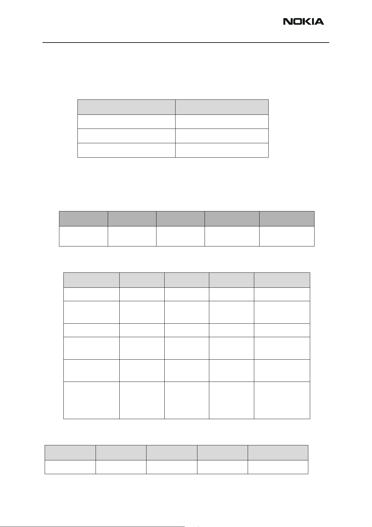
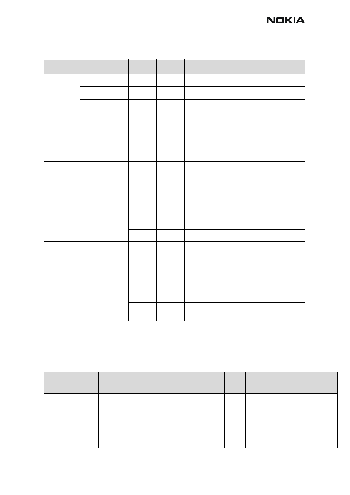
Baseband Technical Specifications
Absolute Maximum Ratings
Signal Note
Battery Voltage (Idle) -0.3V - 5.5V
Battery Voltage (Call) Max 4.7V
Charger Input Voltage -0.3V - 16V
DC Characteristics
Regulators and Supply Voltage Ranges
Battery Voltage Range
Signal Min. Nom Max Note
VBAT 3.1V 3.6V 4.2V (charging
high limit voltage)
BB Regulators
Signal Min. Nom Max Note
VANA 2.70V 2.78V 2.86V I
VFLASH1 2.70V 2.78V 2.86V I
VFLASH2 2.70V 2.78V 2.86V I
VSIM 1.745V
VIO 1.72V 1.8V 1.88V I
VCORE 1.0V
2.91V
1.235V
1.425V
1.710V
1.8V
3.0V
1.053V
1.3V
1.5V
1.8V
1.855V
3.09V
1.106V
1.365V
1.575V
1.890V
3.1V SW cut off
= 80mA
max
= 70mA
max
I
= 1.5mA
sleep
= 40mA
max
I
= 25mA
max
I
= 0.5mA
sleep
= 150mA
max
I
= 0.5mA
sleep
I
= 200mA
max
I
= 0.2mA
sleep
Default value 1.5V
Accessory Regulator
Signal Min Nom Max Note
Vout 2.72V 2.80 2.88V I
max
= 70mA
Page 10 ãNokia Corporation. Issue 1 3/03
Company confidential NPL-3
CCS Technical Documentation System Module and User Interface
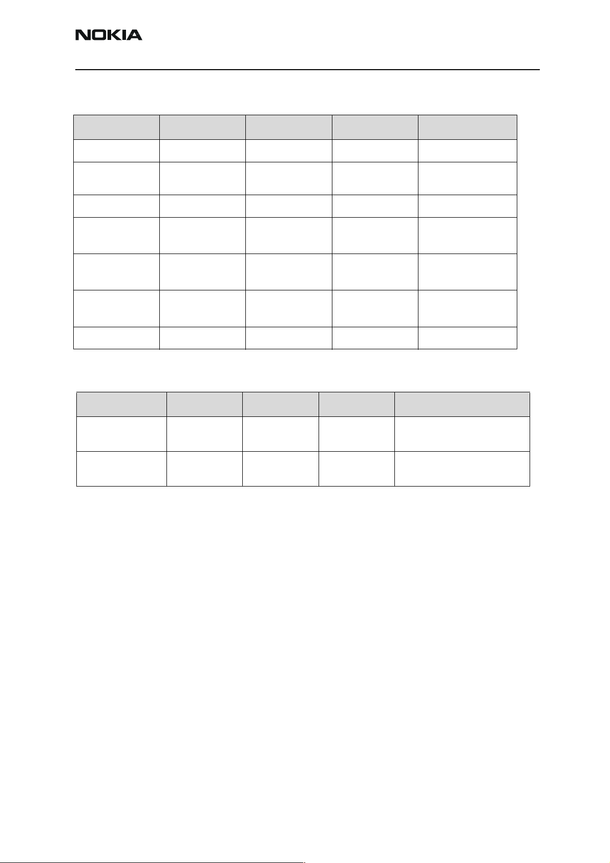
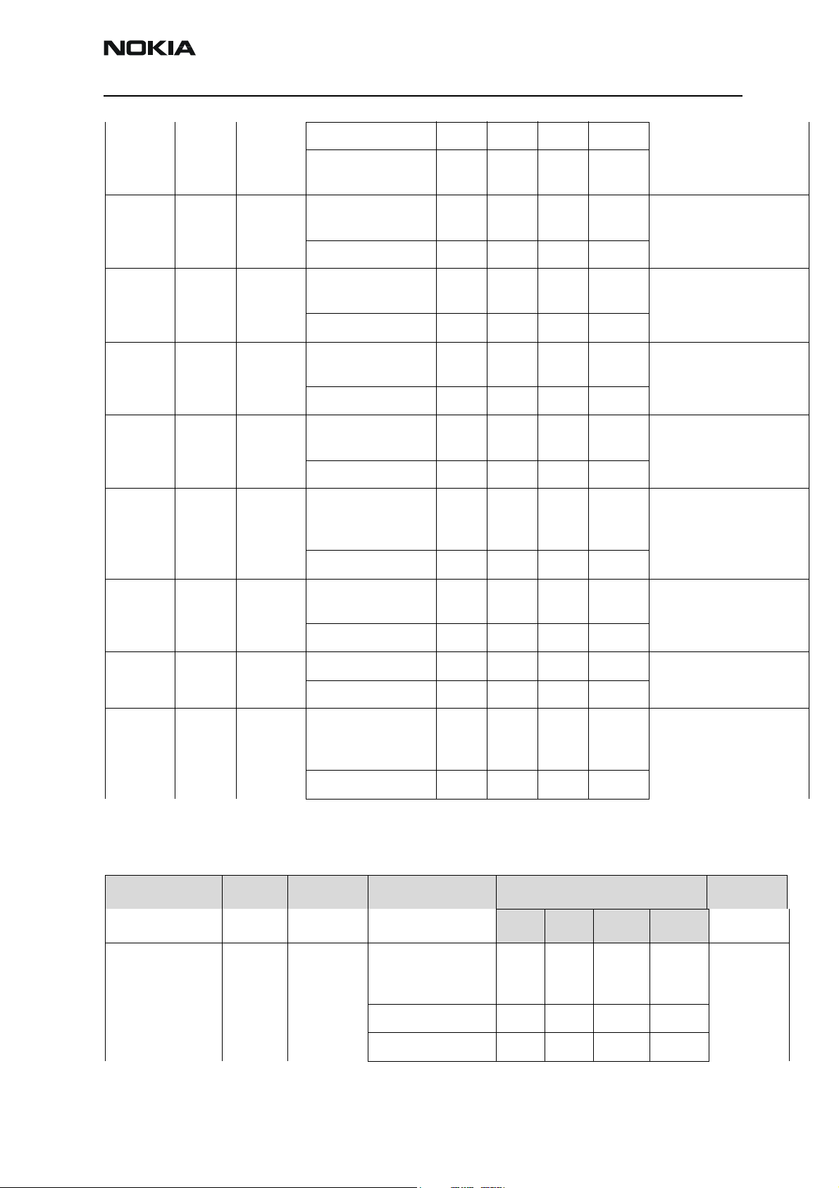
RF Regulators
Signal Min Nom Max Note
VR1A 4.6V 4.75V 4.9V I
VR2 2.70V
3.20V
2.78V
3.3V
2.86V
3.40V
VR3 2.70V 2.78V 2.86V I
VR4 2.70V 2.78V 2.86V I
VR5 2.70V 2.78V 2.86V I
VR6 2.70V 2.78V 2.86V I
VR7 2.70V 2.78V 2.86V I
max
I
max
max
max
I
sleep
max
I
sleep
max
I
sleep
max
= 10mA
= 100mA
= 20mA
= 50mA
= 0.1mA
= 50mA
= 0.1mA
= 50mA
= 0.1mA
= 45mA
Current Sources
Signal Min Nom Max Note
IPA1 and IPA2 0mA - 5mA Programmable, +/-6%
V
IPA1,VIPA1
= 0V - 2.7V
IPA3 and IPA4 50mA 100mA 105mA V
= 0V - 2.7V,
IPA1
UEM Internal
Issue 1 3/03 ãNokia Corporation. Page 11
NPL-3 Company confidential
A
y
System Module and User Interface CCS Technical Documentation
Power Distribution diagram
Baseband
UEM
RF Regulators
VLED+
White LED
Driver
Battery CHACON
VBAT
VBAT
Audio
Ampl ifier
RTC
Regulator
Baseband
Regulators
ccessor
VR1A
VR1B
VR2-7
VSIM
VCORE
VANA
VIO
VFLASH1
VFLASH2
6
SIM
UPP
FLASH
LCD
Backup
battery
FM
Radio
PA Supply
Vout
System Connector
IRDA
VBAT
Page 12 ãNokia Corporation. Issue 1 3/03
Company confidential NPL-3
CCS Technical Documentation System Module and User Interface
Baseband External and Internal Signals and Connections
This section describes the external and internal electrical connection and interface levels
on the baseband. The electrical interface specifications are collected into tables that
covers a connector or a defined interface.
Figure 3: RF/BB connections block diagram
VR3
VBAT
IPA1
IPA2
VR1A
VR2
VR3
VR4
VR5
VR6
VR7
BB
UEM
UPP
AFCOUT
AUXOUT
RXIINP
RXQINP
TXIOUTP
TXIOUTN
TXQOUTP
TXQOUTN
VrefRF01
PATEMP
GENIO5
GENIO6
GENIO7
RFCLK
RFBUSCLK
RFBUSDA
RFBUSEN1X
GENIO9
VCTCXO VCO
VC
TXC
OUT_BB1_I
OUT_BB1_Q
TXI_0
TXI_180
TXQ_180
TXQ_0
VB_EXT
RFTEMP
TXP
RESET
TXA
REFOUT
SCLK
SDATA
SLE
MODE
MODOUTP_G_TX
MODOUTM_G_TX
MODOUTP_P_TX
MODOUTM_P_TX
Helgo
PA
VCP
VRF_TX
VRF_RX
VF_RX
VLNA
VPAB
VLO
VPRE
VBB
Iref_850
Iref_1800_1900
RF
VR7
VR1A
VR2
VR4
VR5
VR6
VBAT
IPA1
IPA2
Issue 1 3/03 ãNokia Corporation. Page 13
NPL-3 Company confidential
System Module and User Interface CCS Technical Documentation
FM Radio Interface
BB Signal FM Radio Signal Min Nom Max Condition Note
VFLASH2 Vcca 2.7V 2.78V 2.86V I
Vcc(vco) 2.7V 2.78V 2.86V I
Vccd 2.7V 2.78V 2.86V I
GenIO(3) FMClk 1.4V
0
30ppm Stability
GenIO(8) FMWrEn 1.4V
0V
GenIO(12) FMCtrlDa 1.4V
0
GenIO(11) FMCtrlClk 1.4V
0
FM Antenna RFI1, RFI2 76 MHz 108 MHz FM Input frequency
1.8V 1.88V
0.4V
32kHz Frequency Also 6.5 MHz can be
1.8V 1.88V
0.4V
1.8V 1.88V
0.6V
1.8V 1.88V
0.6V
1 MHz Frequency
High
Low
High
Low
High
Low
High
Low
=10.5 mA
max
=940 mA
max
= 3.9 mA
max
Reference clock for
FM radio module
used
Write/Read enable
Bi-directional data
FM Radio L
FM Radio R
VAFL
VAFR
100mV Audio level
24 dB 30 dB Channel sep-
aration
54dB 60 dB (S+N)/N
2% Harmonic
distortion
AC and DC Characteristics of RF-Baseband Voltage Supplies
Signal
name
VBAT Battery PA, UEM Voltage 2.95 3.6 4.2 V Battery supply. Cut-off
From To Parameter Min Typ Max Unit Function
level of DCT4 regulators is
3.04V. Losses in PWB
tracks and ferrites are
taken account to minimum battery voltage
level.
Page 14 ãNokia Corporation. Issue 1 3/03
Company confidential NPL-3
CCS Technical Documentation System Module and User Interface
Current 2000 mA
Current drawn by PA
when ”off”
VR1A UEM Helgo Voltage 4.6 4.75 4.9 V Supply for charge pump
Current 2 10 mA
VR2 UEM Helgo Voltage 2.70 2.78 2.86 V Supply for I/Q-modula-
Current 65 100 mA
VR3 UEM VCTCXO,
Helgo
VR4 UEM Helgo Voltage 2.70 2.78 2.86 V Supply for Helgo RX; PA
VR5 UEM Helgo Voltage 2.70 2.78 2.86 V Supply for Helgo PLL;
Voltage 2.70 2.78 2.86 V Supply for VCTCXO, PLL
Current 1 20 mA
Current 50 mA
Current 50 mA
0.8 2 mA
for SHF VCO tuning.
tors, buffers, ALS
digital parts
bias blocks.
dividers, LO- buffers,
prescaler,
VR6 UEM Helgo Voltage 2.70 2.78 2.86 V Supply for Helgo BB and
LNAs
Current 50 mA
VR7 UEM SHF VCO Voltage 2.70 2.78 2.86 V Supply for SHF VCO
Current 30 mA
VrefRF01 UEM Helgo Voltage 1.334 1.35 1.366 V Voltage Reference for
Helgo DCN2 op.amps.
Current 100 mA
AC and DC Characteristics of RF-Baseband Digital Signals
Signal name From To Parameter Input Characteristics Function
Min Typ Max Unit
TXP
(RFGenOut3)
UPP Helgo ”1” 1.38 1.88 V Power
amplifier
enable
”0” 0 0.4 V
Load Resistance 10 220 kW
Issue 1 3/03 ãNokia Corporation. Page 15
NPL-3 Company confidential
System Module and User Interface CCS Technical Documentation
Load Capacitance 20 pF
Timing Accuracy 1/4 symbol
TXA UPP Helgo ”1” 1.38 1.88 V Power con-
trol loop
enable
”0” 0 0.4 V
Load Resistance 10 220 kW
Load Capacitance 20 pF
Timing Accuracy 1/4 symbol
RFBusEna1X UPP Helgo ”1” 1.38 1.88 V RFbus ena-
ble
”0” 0 0.4 V
Current 50 mA
Load resistance 10 220 kW
Load capacitance 20 pF
RFBusData UPP Helgo ”1” 1.38 1.88 V RFbus
data; read/
write
”0” 0 0.4 V
Load resistance 10 220 kW
Load capacitance 20 pF
Data frequency 10 MHz
RFBusClk UPP Helgo ”1” 1.38 1.88 V RFBus
clock
”0” 0 0.4 V
Load resistance 10 220 kW
Load capacitance 20 pF
Data frequency 10 MHz
Mode Select
(GENIO9)
UPP Helgo ”1” 1.38 1.85 V Mode
Selection
”0” 0 0.4 V
RESET
(GENIO6)
UPP Helgo ”1” 1.38 1.85 V Reset to
Helgo
”0” 0 0.4 V
Load capacitance 20 pF
Load resistance 10 220 kW
Timing accuracy 1/4 symbol
Page 16 ãNokia Corporation. Issue 1 3/03
Company confidential NPL-3
CCS Technical Documentation System Module and User Interface
AC and DC Characteristics of RF-Baseband Analogue Signals
Signal name From To Parameter Min Typ Max Unit Function
VCTCXO VCTCXO UPP Frequency 13 26 MHz High stability clock
signal for the logic
circuits, AC coupled. Distorted sinewave e.g. sawtooth.
Signal amplitude 0.2 0.8 2.0 Vpp
Input Impedance 10 kW
Input Capacitance 10 pF
Duty Cycle 40 60 %
VCTCXOGnd VCTCXO UPP DC Level 0 V Ground for refer-
ence clock
RXI/RXQ Helgo UEM Voltage swing
(static)
DC level 1.3 1.35 1.4 V
TXIP / TXIN UEM Helgo Differential voltage
swing (static)
DC level 1.17 1.20 1.23 V
Source Impedance 200 W
TXQP / TXQN UEM Helgo Same spec as for TXIP / TXIN
AFC UEM VCTCXO Voltage Min
Max
Resolution 11 bits
Load resistance
and capacitance
Source Impedance 200 W
1.35 1.4 1.45 Vpp Received demodu-
2.15 2.2 2.25 Vpp Programmable volt-
0.0
2.4
1
0.1
2.6
100
lated IQ signals
age swing.
Programmable common mode voltage.
Between TXIP-TXIN
V Automatic fre-
quency control signal for VCTCXO
kW
nF
TxC UEM Helgo Voltage Min
Max
Source Impedance 200 W
Resolution 10 bits
RFTemp Helgo UEM Voltage at -20oC 1,57 V Temperature sensor
2.4
0.1 V Transmitter power
level and ramping
control
of RF.
Issue 1 3/03 ãNokia Corporation. Page 17
 Loading...