

Page 1
CONFIDENTIAL
Service & Analysis Center Europe
Training Team
version 1.1 / 01.02.2000 Page 1 of 41
Page 2

CONFIDENTIAL
Service & Analysis Center Europe
Training Team
Introduction
IMPORTANT:
This document is intended for use by authorised NOKIA service centers only.
The purpose of this document is to provide some further service information for NOKIA 6150 phones.
It contains a lot of collected tips and hints, to find failures and repair solutions easily.
It will also give support to the inexperienced technicians.
Saving process time and improving the repair quality is the aim of using this document.
We have build it up based on fault symptoms (listed in "Contents") followed by detailed description for further analysis.
It is to be used additionally to the service manual and other service information
like Service Bulletins, for that reason it doesn't contain any circuit descriptions or schematics.
All measurements are made with using of following equipment:
Nokia repair SW : Wintesla Version 6.10
DLL version : NSEKM-13 version 2.41.03
Nokia Module Jig : JBS-19
Digital multimeter : Fluke 73
Oscilloscope : Hitachi V-1565; Fluke PM 3380A
Spectrum Analyzer : Advantest R3361C with an analogue probe
RF-Generator / : Rohde & Schwarz CMD 53
GSM Tester
While every endeavour has been made to ensure the accuracy of this document, some errors may exist. If any errors are
found by the reader, NOKIA should be notified in writing, using following procedure:
Please state:
Title of the Document + Issue Number/Date of publication
Page(s) and/or Figure(s) in error
Please send to: Nokia GmbH
Service & Analysis Center Europe
Meesmannstr.103
D-44807 Bochum / Germany
Email: ams.sace-training@nokia.com
version 1.1 / 01.02.2000 Page 2 of 41
Page 3

CONFIDENTIAL
Service & Analysis Center Europe
Training Team
Contents
INTRODUCTION .................................................................................................................................................. 2
D
OESN'T SWITCH ON
N
OT CHARGING
L
OW STAND-BY TIME
I
NTERMITTENT DOESN'T SWITCH ON
P
HONE SWITCHES OFF ITSELF
S
WITCHES OFF ITSELF - CONTACT SERVICE ON THE DISPLAY
C
ONTACT SERVICE
C
ONTACT SERVICE
C
ONTACT SERVICE
C
ONTACT SERVICE – PPM VALIDITY
C
LOCK TIME OR USER SETTINGS PROBLEMS
B
UZZER FAILURES
I
NTERNAL AUDIO FAILURES
E
XTERNAL AUDIO FAILURES
A
CCESSORY DETECTION FAILURE (HEADSET / CAR KIT ACTIVE
.............................................................................................................................................. 4
..................................................................................................................................................... 7
........................................................................................................................................... 11
....................................................................................................................... 12
................................................................................................................................13
– COBBA
– COBBA
– E
PARALLEL BUS FAILED
..................................................................................................................... 16
SERIAL
EPROM TUNE CHECKSUM FAIL
................................................................................................ 15
............................................................................................... 17
........................................................................................................................ 18
............................................................................................................. 19
................................................................................................................................................ 21
................................................................................................................................... 22
.................................................................................................................................. 24
...................................................................................... 14
)................................................................................... 25
D
ISPLAY FAILURE
K
EYPAD FAILURE
I
SIM CARD ............................................................................................................................................. 30
NSERT
SIM CARD
................................................................................................................................................. 27
.................................................................................................................................................. 29
NOT ACCEPTED
, SIM LOCK
FAILURE
................................................................................................... 32
SIM LOCK DATA NSM-1................................................................................................................................. 34
T
HE PHONE HANGS UP AFTER ENTERING THE
L
OW RECEIVER SIGNAL STRENGTH INDICATOR
N
O SERVICE
C
ALL BREAKS
N
O CALL / SERVICE
N
O OR LOW
........................................................................................................................................................ 36
/ N
O SERVICE
.................................................................................................................................. 39
O.K....................................................................................................................................... 39
TX – P
................................................................................................................................... 39
OWER
PIN-
.......................................................................................................... 36
........................................................................................... 35
CODE
version 1.1 / 01.02.2000 Page 3 of 41
Page 4
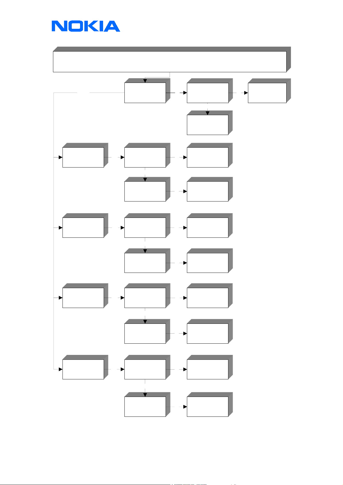
Doesn't switch on
Figure 1: doesn't switch on troubleshooting
Phone doesn't switch on
CONFIDENTIAL
Service & Analysis Center Europe
Training Team
Observe power con-
sumption norm. < 6mA
pulsing to 20mA
(without backlights)
Yes
Check VBAT (3,6V)
N100 / 8, 12, ...
Yes
Check 32,768 kHz
N100/46=1,3Vpp (Sinus)
N100/47=2,3Vpp(Square)
Yes
Check DC Volt. PWRONX
N100 / 29 = VBATT (3,6V)
If Pwr button is pressed
PWRONX = 2,9V
Yes
Check DC Volt. PURX
N100 / 54 = 2,8V
D200 / 122 = 2;8V
(after pressin g Pwr b utton)
Yes
Check Sleep clk 32,768kHz
N100/ 4 8 = 2,8Vpp
D200/124=2,8Vpp(square)
Yes
higher
No
No
No
No
No
Check
C680, C682
Check c onnection
to X101
L103
Change
B100
Check:
R118 (10K)
X300
UI-module
Check s ol derings
of N100
or
Change N100
Check s ol derings
of N100
or
Change N100
No
consumption OK
change
N502
Lift L5 60
(VBATT for Pwr
Amp)
OK
N501 or N502
faulty
insert L560
and lift L654 and
Pin 12, 13 of N502
observe the power
consumption
consum ption not OK
change
N501
Check DC Volt SL E EP X
D200 / 113 = 2,8V
N100 / 24 =2,8V
Yes
Check DC Volt VXO
N100 / 25 = 2,8V
G600 / 1 = 2,8V
Yes
Check VCXO 13MHz
G600 / 2 = 1Vpp
D200 / 93 = 0,6Vpp
Yes
Try to flash
the phone
No
No
No
No
Check s ol derings
of D200
or
Change D200
Check s ol derings
of N100
or
Change N100
Change
G600
See Section:
Can't Flash the
phone
version 1.1 / 01.02.2000 Page 4 of 41
Page 5

CONFIDENTIAL
N100 faulty/ poor soldering
Check if voltage on Pin 29 decreases to 700 mV during pressing the Power on button
•
Check if there is a 32.768 kHz square wave on Pin 48
•
Check if PURX Pin 54 goes up to 2.8 V DC
•
Check if VXO Pin 28 goes up to 2.8 V DC
•
B100 faulty 32,768 kHz
Check 32.768 kHz ; 1 Vpp clock signal on B100
•
G650 faulty 13 MHz
Check VXO 2,8V DC on pin 1 from G650
•
Check 13 MHz; 1 Vpp on output pin 2
•
S001 User Interface
Check if voltage on Pin 29 decreases to 700 mV during pressing the Power on button
•
Service & Analysis Center Europe
Training Team
X300 UI Connector bent out
Check if voltage on Pin 29 decreases to 700 mV during pressing the Power on button
•
R118 missing/ poor soldering
Check if voltage on Pin 29 decreases to 700 mV during pressing the Power on button
•
D200 MAD faulty/ poor soldering
Check 32.768 kHz square wave on Pin 124 (comes from CCONT Pin 48)
•
Check 13 MHz on Pin 93 (comes from G650)
•
Check VBB 2.8 V DC
•
Check PURX 2.8 V DC on Pin 122 (comes from CCONT Pin 54)
•
Check SLEEPX 2.8 V DC 0n Pin 113
•
Resolder MAD completely
•
D210 FLASH faulty / poor soldering/ empty
Check VBB 2.8 V DC on Pin 37
•
If power consumption is around 20mA try to flash the phone
•
Resolder FLASH completely
•
L103 faulty/ poor soldering
Check VB on J232 or pin 8 from CCONT
•
X101 / X102 contacts bend out/ dirty
Check if VBATT and Gnd are connected
•
version 1.1 / 01.02.2000 Page 5 of 41
Page 6
CONFIDENTIAL
N501 / N502 short circuit
If there is a short circuit on VBATT, lift L560 and check again
•
If the current is OK one of the two PA is faulty
•
Assemble L560 back and lift L654 and pin 12 and 13 from N502
•
If the current is OK N502 is faulty, if not N501 is faulty
•
If the PCB is burnt, swap the phone
•
C680; C682 / short circuit
Lift the capacitor and check again
•
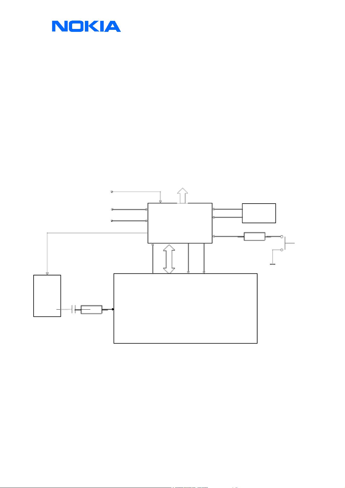
Figure 2: Block diagram of switching on routine
BB Regulator VBB 2.8V
VBATT
Service & Analysis Center Europe
Training Team
VCXO
13 MHz
G600
C213
R103 / R104
VCHAR
BTEMP
R213
SLEEPX
12, 16, ...
60
63
25 VXO 2.8V
24
113
2.8V
55
CCONT
N100
GENSIO
48
124
32 KHz
square
54
122
2.8V
46
47
29
PURX
B100
32 KHz
Crystal
R118
Pwr OnX
from
UI module
MAD2
93
D200
version 1.1 / 01.02.2000 Page 6 of 41
Page 7
Not charging
check VCH on pi n 1,
16 of N101, CHAPS
CONFIDENTIAL
Service & Analysis Center Europe
Not charging (1)
no confirmation / er r or mes sage / beep is coming from phone, if charger i s
plugged in
Check X100, F101,
check V100, C103 if
VCH is short circuited
Ok
No Ok
L104, L105 if
connection to charger
is open
Training Team
check solderi ngs of
N101 or change if
necessary
Do the battery
management
calibration
check the power
consumption of t he
phone (1-5mA if
phone is swit ched on
wit hout SIM & lights)
Phone doesn't stop charging
if any A/D value is
Ok
No
Ok
wrong, refer to
section not charging
(2)
If the power
consumption is
higher, refer to
section low standby
time
Yes
Yes
not charging (2)
low standby time
No
check DC voltage on
pin 2 of D200, M AD,
switches from 2,8V to
0V, if battery is fully
charged
No
resolder or change
MAD if necessary
version 1.1 / 01.02.2000 Page 7 of 41
Page 8
CONFIDENTIAL
Service & Analysis Center Europe
Training Team
failed
Charger voltage failed
Battery siz e
failed
error message ("not charging") / beep is coming from phone, if charger is plugged in
Not charging (2)
Do the battery
management calibration
check DC voltage on pin
Yes
Yes Ok
60 of N100/ C CONT
if char g e r i s pluged in
nomin al VCH 1:10 (0, 8V)
No
check F101, L104, V100,
C103 and voltage
devider R103, R104
check DC Voltage on pin
62 of N100, C CONT
check DC voltage on pin
9 of N101, CHAPS if
Ok
charger is plugged in
resol d er or change D2 00
resol d er or change N1 00
Ok
Ok
try the c al i b ration aga in
resol d er or change N1 00
(2,8V)
No
if necessary
if necessary
if necessary
Try charging, if no A/D
Ok
value was wrong
Battery temperature
failed
Charge current
failed
check battery, X101,
voltage devider R120,
check DC voltage on pin
Yes
Yes
63 of N100, C CONT
check battery, X102,
voltage devider R120,
check DC voltage on pin
No
try the c al i b ration aga in
R122
No
R122
2 of N100, CCONT
No
check N101, R131 try the c al i b ration aga in
Ok
resol d er or change N1 00
Ok
try the c al i b ration aga in
Ok
resol d er or change N1 00
Ok
Ok
if necessary
if necessary
version 1.1 / 01.02.2000 Page 8 of 41
Page 9

CONFIDENTIAL
F100 faulty
Check resistance of F100 (0Ω)
•
V100 faulty
Check resistance of V100 (50KΩ in circuit)
•
C103 faulty short circuit on Vcharge
Check resistance of C103 (50KΩ in circuit)
•
NOTE! V100 is connected in parallel to C103
•
L104 faulty Vcharge
Check resistance of L104 (0Ω)
•
L105 faulty Charge ground
Check resistance of L105 (0Ω)
•
N101 faulty/ poor soldering
Check PWMOUT on Pin 7 (1 Hz standard charger / 32Hz fast charger)
•
Check if CHARLIM on Pin 9 is 2.8V DC
•
Service & Analysis Center Europe
Training Team
N100 faulty/ poor soldering
Change if any A/D value is out of limit but the DC voltages are ok.
•
If DC voltages are wrong, check corresponding voltage dividers
•
Check PWMOUT on Pin 56 (1 Hz standard / 32 Hz fast)
•
X100 faulty/ poor soldering
Check connection of Vcharge; charge ground; charge control
•
X101 BSI; X102 BTEMP
Check connection if battery size or battery temp A/D are out
•
of limit
V102 faulty
Check if there is a short circuit in charge control line
•
Energy management Calibration
If charging stops too early
•
If message “not charging” appears on LCD
•
If any part in charging circuit has been changed
•
If any A/D value is out of limit, check the corresponding
•
DC Voltages on CCONT
version 1.1 / 01.02.2000 Page 9 of 41
Page 10
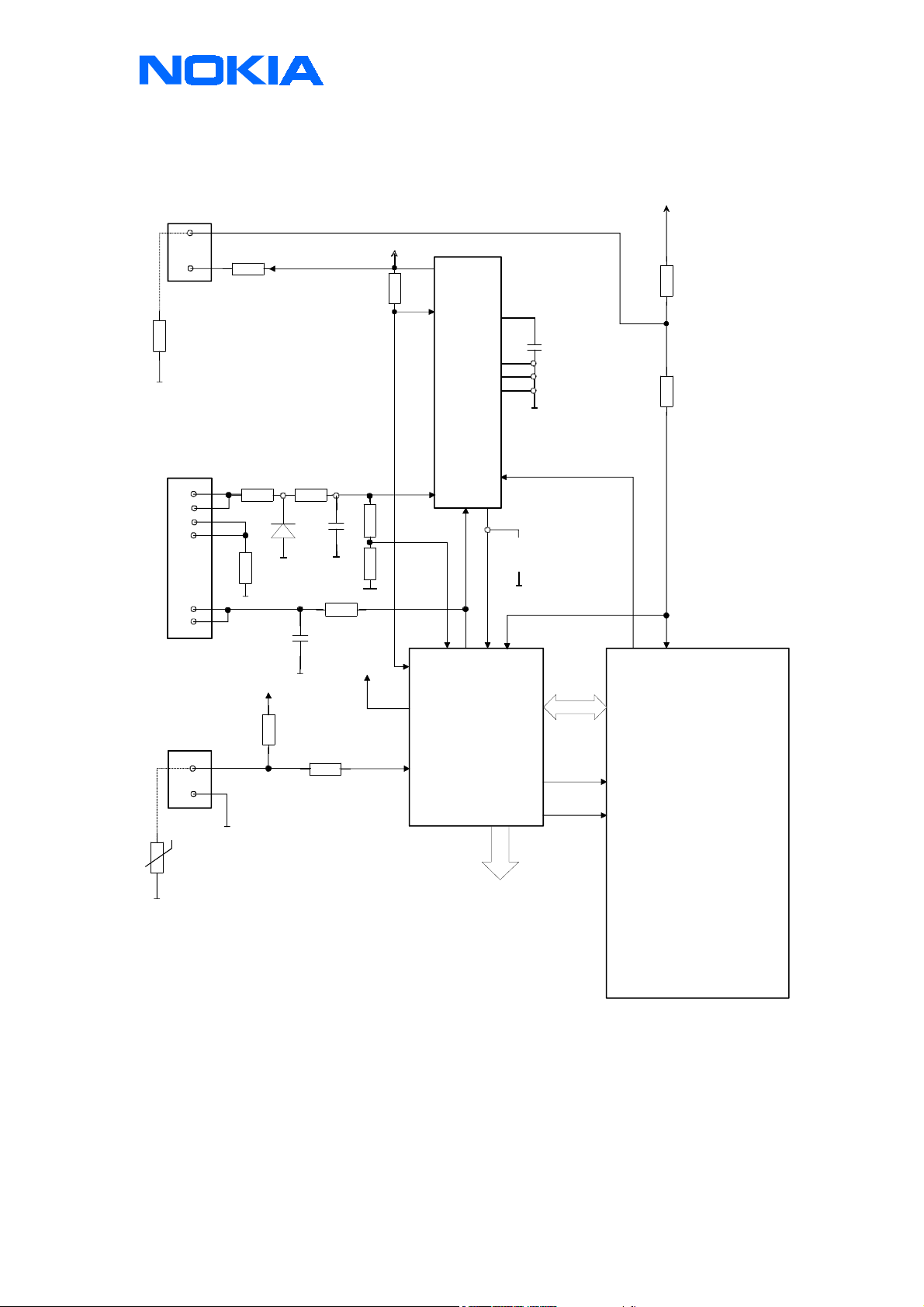
Figure 3: Block diagram of charging concept
CONFIDENTIAL
Service & Analysis Center Europe
Training Team
X101
Battery connector
1
2
BSI Resistor (Inside of Battery)
2.2K .... 18K : NiCd Battery
20K .... 24K : Service Battery
27K .... 51K : 4.1V Lithium Battery
68K .... 91K : 4.2V Lithium Battery
X100
Sysrem Connector
1
3
2
14
4
5
X102
Battery Connector
BTEMP
BGND
T
47K NTC
BTEMP Resistor
inside of Battery
BSI
BVOLT
L103
F101
L105
Charger Ctrl.
VREF
V100
R120
L104
C103
R122
Current
Shunt
R104
R103
R116
VCH
VB
VB
R131
Chargedet.
1,16
2 ICHAR
8,12,16,21,
27,28,57
63
12
5
2,3,4
6,11,13
14,15
N101
CHAPS
710
VBACK
PWMOUT 1Hz / 32Hz
VCHAR
60 56 46 62
N100
CCONT
BB and RF
Regulators
8
9
2.5V DC min
DataClk 49
DataSelX 50
DataI/O 51
CCONTInt 52
Purx 54
C104
CHARLIM
G100
RTC Battery
Battery Type (BSI)
VBB
2
MCUGENOUT
119 DataSCLK
116 GenCCONTCSX
118 GenSDIO
123 CCONTInt
122 Purx
95
CardDetX
R120
R122
D200
MAD2
version 1.1 / 01.02.2000 Page 10 of 41
Page 11
Low Stand-by time
CONFIDENTIAL
Low standby time
(battery is Ok)
Service & Analysis Center Europe
Training Team
check power
cons ump tion of the
phone:
Off state > 0-1mA
sleep mode > 1- 5 mA
Call mode >
200-500mA (lev el 19 / 5)
Ok
check the charging
circuit, use battery
management
calibration
Ok
check if sleep mode
function works
properly
No
change N5 50 , if
cons ump tion is Ok
refer to section "not
No
charging (2)" if any
A/D value is wrong
resold er or change
No
lift L560 lift L103
Ok
D200, MAD if
necessary
No No
change N100,
CCONT if
cons ump tion is Ok
"not charging (2)"
check C142,
C610-12, C105,
N101, change if
necessary
Ok
section
Ok
Calibrate RX and TX
values of the phone
Note: The standby time depends also on the network side, like: PRP (paging repeat
period time), signal strength (min -98dBm), location updates
and on the user handling of the phone (lights on or of, memory acti viti es, games etc.)
No
Ok
refer to section
receiver /
transmitter failure
section "receiver /
transmitter failure"
N501 / N502 / N100 / N101 / D200 / Battery calibration - faulty
Check the current consumption in different operation modes
•
version 1.1 / 01.02.2000 Page 11 of 41
Page 12
CONFIDENTIAL
Service & Analysis Center Europe
Training Team
Figure 4: current consumption values
Function mode Minimum current in mA Maximum current in mA
Off state 0 1,35
Sleep mode 1 5
Call mode GSM 900 250 440
Call mode GSM 1800 200 420
Disconnect the PA's N501 / N501 lift L560 and check the current again
•
Check if the current consumption comes from the first or second side of CCONT lift L103
•
Check C105, C142 or N101
•
Check solderings of the MAD
•
Change MAD
•
calibrate battery value if charging stops too early or battery is too hot after charging (see also chapter "Not charging)
•
Note! The Standby-time depends on the network side and on the user handling
Intermittent doesn't switch on
D210 FLASH faulty
Check if the handset switches on after removing the battery for few seconds
•
or after connecting it with the charger or headset
D210 Flash internal fail
•
version 1.1 / 01.02.2000 Page 12 of 41
Page 13
Phone switches off itself
CONFIDENTIAL
Phone intermittend switches off
Yes
Service & Analysis Center Europe
Training Team
Check if this happens
only w ith 5V S IM-cards
and if the phone work s
probably w ith 3V S IM's
Yes
Check the 5V
supply voltage on
C131 with an
oscilloscope
Yes
Change C131 if the
noise is higher than
350mVpp
Check X101 and
No Wrong
X102, if poor soldered,
bent, soiled or old
version
No
Check amplitude of
32,768KHz square
wave at pin 124 of
MAD (2,8Vpp)
No
Check amplitude of
13MHz at pin 93 of
MAD (600mV pp)
Wrong
Wrong
Resolder, or change
the connector
Change or check
soldering of B100,
N100, R154, C101,
C102
Change or check
soldering of G650,
V600...
No
Check VBB 2,8V DC
on pin 55 of N100
Wrong
Change or check
soldering of N100,
C107
version 1.1 / 01.02.2000 Page 13 of 41
Page 14
CONFIDENTIAL
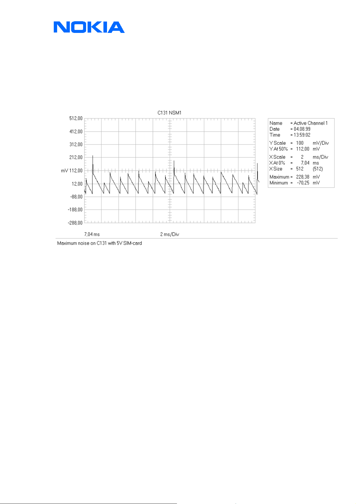
C131 10μF/10V
Check if the handset works with 3V SIM-cards
•
Check if the 5V voltage over the capacitor C131 is around 4,8V-5,2V with
•
maximal 350mVpp noise overlap (look at the diagram below)
Figure 5: maximal noise o n C131
Service & Analysis Center Europe
Training Team
Switch off itself - contact service on the display
D200 MAD faulty / poor soldering
Check the amplitude of the 32,768 kHz square wave on pin 124 (comes from CCONT pin 48)
•
Check the amplitude of the 13 MHz clock frequency pin 93 (from G650)
•
Check VBB 2,8V DC
•
Resolder MAD
•
Internal error of MAD
•
version 1.1 / 01.02.2000 Page 14 of 41
Page 15

CONFIDENTIAL
Contact service – COBBA parallel bus failed
Contact Service
Check via WINTESLA / Testing / Sel ftest
which kind of selftest is fail
COBBA parallel bus
failed
Yes
Service & Analysis Center Europe
Training Team
check COBBACLK
13MHZ/ 3,2Vpp on
pin 45 0f COBBA
Ok
check VBB 2,8V on
pin 27, 53 of COBBA
Ok
Check VCOBBA 2,8V
DC on pin 7, 12, 21,
25 of COBBA
Ok
Check soldering of
MAD or change MAD
No
No
No No
Check COBBA Clk on
pin 144 of MAD
Check VBB 2,8V DC
on pin 55 of N100,
CCONT
Check VCOBBA 2,8V
DC on pin 22 of
N100, CCONT
No
No
Change or check
soldering of MAD
check soldering or
change N100, C107
Change or check
soldering of N100,
C133
Ok
Check soldering of
COBBA or change
COBBA
version 1.1 / 01.02.2000 Page 15 of 41
Page 16

Contact service – COBBA serial
Contact Service
Ch eck via W INTES LA / Testing / S elf test
which kind of selftest is faulty
COBBA Serial
bus failed
Yes
CONFIDENTIAL
Service & Analysis Center Europe
Training Team
Check VBB 2 ,8V
DC on pin 27, 53
of COBBA
Ok
Check VCOBBA
2,8V DC on pin 7,
12, 21, 25 of
COBBA
Ok
Check soldering
of COBBA or
change CO BBA
Ok
Check soldering
of MAD or change
MAD
No
No
Check VBB 2 ,8V
DC on pin 55 of
N100, CCONT
Check VCOBBA
2,8V DC on pin
22 of N100
No
No
Change or check
solder ing of
N100, C140
Change or check
solder ing of
N100, C133
N250 COBBA faulty / poor soldering
Check VBB 2,8V DC on pin 27, 53 from COBBA
•
Check VCOBBA 2,8V DC on pin 7,12,21,25, from COBBA
•
Check COBBACLK 13MHz 3,2Vpp pin 45 from COBBA
•
Resolder COBBA
•
Internal error of COBBA
•
Note! Rewrite SIMLOCK and IMEI entries with use of the Nokia security SW (SSSW) and make a SW-update or send these
phones to the SACE, if this procedure is not permitted to you
version 1.1 / 01.02.2000 Page 16 of 41
Page 17

CONFIDENTIAL
Contact service – Eeprom tune checksum fail
Contact Service
Check via WINTESLA / Testing / Selftest
which kind of selftest is fail
EEPROM tune
checksum fail
Yes
Service & Analysis Center Europe
Training Team
Check via WINTESLA >
product information, if
any phone data, like:
IMEI, product code,
PSN, etc. is corrupted
change the EEPROM if
it is permitted to you to
Reset the phone (don't
No
Yes No
rewrite the IMEI
use the full factory set if
it is not permitted to you
to rewrite the IMEI)
EEPROM
internal fault
send this phone to the
SACE if it is not
permitted to you to
rewrite the IMEI
refer to General
Service Bulletin
037!!!
Phone is Ok, if
CONTACT SERVICE
dissapears
D230 Eeprom faulty
Check with Wintesla if IMEI or product data are corrupted
•
Don’t use the "Full factory set" with Wintesla, otherwise the IMEI will be changed to question marks
•
Change the Eeprom if it's permitted to you and write all ID data (IMEI, product code…) back
•
If you aren't allowed to change the Eeprom and the IMEI is missing, write a note with a little comment, and send it
•
together with the phone to the SACE
version 1.1 / 01.02.2000 Page 17 of 41
Page 18

CONFIDENTIAL
Service & Analysis Center Europe
Training Team
Note! Rewrite SIMLOCK and IMEI entries with use of the Nokia security SW (SSSW) and make a SW-update or send these
phones to the SACE, if this procedure is not permitted to you
Contact service – ppm validity
Contact Service
Check vi a WINTESLA / Tes t ing / Selftest
which kind of selftest is fail
PPM v alidity fail
try to flash the phone
check soldering or
change D200,
SW / D210 Flash faulty / poor soldering
Check if the fault disappears after a SW-update
•
Resolder D210 Flash
•
Internal error of Flash
•
Yes
not OK
FLASH
OK
phone is OK, if
CONTACT
SERVICE dissapears
after flashing
version 1.1 / 01.02.2000 Page 18 of 41
Page 19

Clock time or user settings problems
Clock time problems / wrong ringingtone speed
check 32,768KHz
clock frequency on
pin 48 of N100,
CCONT
Check soldering or
change B100, R 154 ,
C101, C102, N100
CONFIDENTIAL
Service & Analysis Center Europe
Training Team
Clock time / Ringing tone is too fast or too slow
32,786 kHz Sleep oscillator
Check that the sleepclk 32.768 kHz square wave frequency on pin 48 CCONT is not higher or lower
•
Check the crystal B100, R154, C101, C102, N100
•
Clock freezes after switching on the phone
Yes
Check the
CCONTINT
impulse on pin
52 of N100,
CCONT
Ok
Check the
CCONTINT
impulse on pin
123 of D200,
MAD
No
No
resolde r C CONT
or change if
solderings are
esolder MA D or
r
change if
solderings are
Ok
Ok
version 1.1 / 01.02.2000 Page 19 of 41
Page 20

CONFIDENTIAL
Clock freezes after power on
CCONTINT short circuit / break
Check the CCONTINT impulse on pin 52 CCONT or pin 123 MAD (see the diagram below)
•
Check pin 52 CCONT pin 123 MAD short circuit or break
•
Figure 6: CCONTINT impulse
Service & Analysis Center Europe
Training Team
Loose of clock time after removal of battery
Backupbattery
keeps the clock
running for min.
10 minutes
No
Check the DC
voltage 2,8V -
3,3V on G100,
backupbattery
No
Check the
springcontacts if
they are bent or
soiled
No
Change G100,
backupbattery
Yes
correct or clean
the contacts
version 1.1 / 01.02.2000 Page 20 of 41
Page 21

CONFIDENTIAL
Service & Analysis Center Europe
Looses clock time if the battery is empty or removed for a few minutes
G100 Back up battery faulty / disconnected
Check the voltage 2,8V-3,3V over the back up battery connected to the PCB in the service modus
•
Check the spring contacts
•
Clean the contacts for the back up battery on the board
•
Buzzer failures
Buzzer failure
check buzzer signal 1Vpp
on B001, buzzer
use WINTESLA / testing /
audio / level 1, 1000Hz
Ok
change B001, buzzer
Training Team
check 32,768KHz on pin
48 of N100, CCONT if
speed of buzzer is too
slow or fast
No
check contacts and
solder of X300
Ok
check buzzer signal
200mV pulses on pin 97
of D200, MAD (use same
settings)
not Ok not Ok
Change B100
not Ok
No
resolder or change X300 if
any spring is bended
resolder or change MAD if
necessary
check solder of R154,
C101, C102 or change
N100 if necessary
B001 / UI-module
Check buzzer signal about 1Vpp pulses (use WINTESLA / testing / audio
•
Level 1, 1000Hz)
Change component if signal is ok
•
version 1.1 / 01.02.2000 Page 21 of 41
Page 22

CONFIDENTIAL
X300, board to board connector
Check soldering
•
Check contact springs, change component if bent
•
D200, MAD
Check buzzer signal on Pin 97 (200mV pulses) use WinTesla / testing / audio
•
Level 1, 1000Hz
B100, 32.768 kHz crystal
Change component if ringing tone speed is too low or high if a call comes in.
•
If you pick a ringing tone from the menu, the speed is normal.
In this case, also the clock is running wrong if the phone is switched off.
•
Internal Audio Failures
Internal audio failure
Service & Analysis Center Europe
Training Team
speaker doesn't
work
(receiving audio)
microphone
doesn't work
check impedance
Yes
of speak er (30
Ohm)
Ok
resolder or change
X300 if an y sp r ing
is bent
check contacts
and impedance of
Yes not Ok
microphone (800
Ohm)
Ok
check soldering
and conta cts of
X100
Ok
check MIC BIAS
voltage, 2,8V DC if
audio is active
Ok
not Ok
not Ok
not OK
not Ok
change speaker
check soldering of
N250, COBBA or
change if
necessary
change
microphone
resolder or change
if necessary
change C266
check if MIC N or
MIC P is short
circuited to ground
Ok
check solder of
N250, COBBA or
change if
necessary
not Ok
change V103
version 1.1 / 01.02.2000 Page 22 of 41
Page 23

CONFIDENTIAL
Speaker
No / quiet / distorted receiving audio signal
Check the mechanic of speaker, contacts, membrane, soiling
•
Check resistance of speaker (about 30Ω)
•
Microphone
No / quiet / distorted transmitting audio signal
Check contacts of microphone
•
Check resistance of microphone (about 800Ω)
•
X300
Check soldering
•
Check contacts (change connector if bent)
•
X100
Check microphone spring contacts
•
Check soldering
•
Service & Analysis Center Europe
Training Team
V103
Check resistance from MIC N or MIC P to ground (about 1KΩ and 2KΩ)
•
change component if resistance is 0
Ω
C266
Check MIC BIAS voltage 2.8V DC collector V 250 if audio is active (use WinTesla / testing / audio)
•
version 1.1 / 01.02.2000 Page 23 of 41
Page 24

External Audio Failures
CONFIDENTIAL
External audio failures
Service & Analysis Center Europe
Training Team
XEAR failure
(receiving audio)
XM IC failure
(transmitting
audio)
check X100
Yes not oK
Yes not oK
if poor soldered
or soi led
contacts
oK
check L107
(0 Ohm)
check X100
if poor soldered
or soi led
contacts
oK
not oK
resolder or clean
X100,
change if
necessary
change L107
resolder or clean
X100,
change if
necessary
check L106 (0
Ohm)
not oK
change L106
L106
Check resistance of coil (0Ω), if there is no XMIC
•
L107
Check resistance of coil (0Ω), if there is no XEAR
•
X100
Check soldering
•
Check contacts (soiling)
•
version 1.1 / 01.02.2000 Page 24 of 41
Page 25

CONFIDENTIAL
Accessory detection failure (headset / car kit active)
Accessory detection failure
(headset / car kit active)
check if XMIC
headset is
detected
Yes not oK
(X100 pin 8) i s
short circui ted to
ground
oK
Service & Analysis Center Europe
Training Team
change V102
car kit is
detected
check if there is a
liquid damage
around X100,
V102, V101, L105
check R257,
R256, R261
check if XEAR
Yes not oK
(X100 pin 10) i s
short circui ted to
ground
oK
check R259,
R260
not oK
not oK
resolder or
change if
necessary
change V102
resolder or
change if
necessary
V102
Check the resistance of XMIC to ground if headset is detected
•
Check the resistance of XEAR to ground if car kit is detected
•
Change component if resistance is low
•
R259 / R260
Check soldering and resistance of components if car kit is detected
•
(45KΩ / 22KΩ inside PCB)
R256 / R257 / R261
Check soldering and resistance of components if headset is detected
•
(2,2KΩ, 45KΩ, 22KΩ inside PCB)
version 1.1 / 01.02.2000 Page 25 of 41
Page 26

CONFIDENTIAL
Liquid damage
Check if there is a liquid damage around X100, V101, V102 and L105)
!
Figure 7: Block diagram of audio switching concept
VBB 2.8V
R259
R260
R261
C261 C260
VCOBBA 2.8 V
107 HOOKDET
MAD2
D200
108 HEADDET
CCONT
64 EAD
N100
Service & Analysis Center Europe
Training Team
System Connector
X100
XEAR 10
SGND 9
XMIC 8
V102
V102
V102
R256
R254
R257
C255
R252
C254
C272
C253
C258
C257
2 AUXOUT
3 HF
58 MIC 3P
62 MIC 1P
61 MIC 1N
57 MIC 3N
COBBA
N250
version 1.1 / 01.02.2000 Page 26 of 41
Page 27

Display Failure
contrast
dissapears,
missing segments
Yes
CONFIDENTIAL
Display failure
change elastomer
not oK
change LCD, if
elastomer change
doesn't help
Service & Analysis Center Europe
Training Team
strange signs on
LCD, "dark" LCD
during start up is
missing
black line on LCD
after phone is
switched off
Yes
Yes
not oK
check contacts
and solderin gs of
X300
check LCD reset
on pin 36 of MAD
add a 4,7M Ohm
resistor to C6 on
user i nterface
(piggypack)
not oK
not oK
resolder or change
X300 if any s pr ing
is bent
resolder M AD or
change if
necessary
refer to service
bulletin 009 NSE-1
version 1.1 / 01.02.2000 Page 27 of 41
Page 28

CONFIDENTIAL
Service & Analysis Center Europe
Training Team
Elastomer
Change Elastomer to recommended blue ShinEtsu elastomer MSG in Tape & Reel. Do not touch elastomer with bare
•
hands (see SB035 NSM-1).
Figure 8: different types of elastomers
DO NOT USE #5409131 #9780252
ANY LONGER Recommended Elastomer
LCD / UI Module
Change LCD if elastomer change doesn't help
•
The PCB version UE4_13 makes better contact between PCB and the Elastomer, pad size of the LED's is modified
•
Figure 9: different types of LCD's
Philips LCD Seiko LCD
N0 capacitors capacitors inside
version 1.1 / 01.02.2000 Page 28 of 41
Page 29

CONFIDENTIAL
Service & Analysis Center Europe
Training Team
X300
Check solderings
•
Check contacts (change connector if bent)
•
D200
If there are wrong signs on LCD and the filled LCD during start up is missing, check LCD reset on JBS-19 Test Pin 25 or
•
D200/ 36 during start up
UI-module
Check LCD contact pads, clean if soiled
•
Change if elastomer and LCD change do not help
•
Keypad failure
Keypad failure
check contacts
and solderings of
X300
oK
check keys on UI
module
oK
check ROW and
COL lines of D 200,
MAD
not oK
not oK
not oK
resolder or cha nge
X300 if any spring
is bent
change module if
any key is
damaged
resolder MAD or
change if
necessary
X300
Check soldering
•
Check contacts (change connector if bent)
•
D200
• Check ROW (5:0) and COL (4:0) lines
UI-module
• Check keys on UI, change UI-module if any keydome is damaged
version 1.1 / 01.02.2000 Page 29 of 41
Page 30

Insert SIM CARD
CONFIDENTIAL
Insert SIM card
the phone does n't register the SI M card
Service & Analysis Center Europe
Training Team
check s olderings and cont acts of
X300, SIM ca rd reader
oK
check pin 95 of D200 MAD, if BSI
is connected
oK
check pin 120 (SIMDATA ), pin
126 (SIMCLK), pin 127(SIMRST),
pin 128 (SIMIOC) and pi n 129
(SIMPWR) of D200, M AD
oK
check pin 43 (SIMDATA), pin 38
(SIMCLK), pin 42 (SIMRST), pin
36 (VSIM) of N100, CCONT
not oK
not oK
not oK
not oK
resolder X300 or
change if any
contact is bent
check solderings
and contacts of
connector X101
resolder MAD or
change if necessary
resolder CCONT or
change if necessary
not oK
not oK
not oK
swap t h e phone if
any wire to the SIM
card reader has torn
off
check the battery
contacts, clean if
soiled
change V104 if SIM
-DATA, -CLO CK,
-RESET or VSIM is
short circuited to
ground
X302, SIM card reader
Check soldering
•
Check contacts (change connector if bent)
•
X101, battery connector
Check BSI connection to D200 / 95 CardDetX
•
version 1.1 / 01.02.2000 Page 30 of 41
Page 31

CONFIDENTIAL
D200, MAD
Check SIM card -DATA (Pin120), -Clock 3,25MHz (Pin 126), -Reset (Pin 127), -IOC (Pin 128)
•
and -Power (Pin 129)
N100, CCONT
SIM card -DATA (Pin 43), -Clock 3,25MHz (Pin 38), -Reset (Pin 42) and VSIM 3V/5V DC
•
(Pin 36) depends on SIM card
V104
Change component if SIM -DATA, -Clock, -Reset or VSIM is short circuited to
•
ground
Service & Analysis Center Europe
Training Team
version 1.1 / 01.02.2000 Page 31 of 41
Page 32

CONFIDENTIAL
SIM card not accepted, SIM LOCK failure
SIM card not accepted (SIM LOCK active)
SIM card not
accepted
appears on
LCD after
entering the
PIN code.
Yes
Service & Analysis Center Europe
Training Team
open
WINTEASLA
and activate
quick /RF -info
compare the data
entries MCC+MNC
Yes Ok
with the listed
entries of t he
respective product
code
not oK
SIM LOCK is oK!
correct the SIM
LOCK settings
with use of the
Nokia security SW
(SSSW) or send
those phones to
the SACE
if SIMLOCK is not
active, but
phone still doesn't
accept SIM,
change N250,
COBBA
!!!Take note!!!
if the Msin data field is
closed to any special
IMSI number range,
the operator is
ONLY
allowed to open the
SIM LOCK!!!(see
General SB065)
correct the SIM LOCK
settings with use of
the Nokia security SW
(SSSW) aft er
changing of C OBBA
or send those phones
to the SACE
If message "SIM Card not accepted" appears on LCD after entering PIN code,
•
a SIM LOCK is activated in this phone.
Initialise phone into normal mode and activate
•
Quick/ RF-info
(WinTesla)
compare the SIM LOCK entries with the references from the operator
N100, CCONT
Refer to insert SIM Card procedure
•
version 1.1 / 01.02.2000 Page 32 of 41
Page 33

CONFIDENTIAL
Service & Analysis Center Europe
Training Team
N250, COBBA
Change COBBA if all SIM LOCK entries and SIM card signals
•
from CCONT are ok
Note! Rewrite SIMLOCK and IMEI entries with use of the Nokia security SW (SSSW) and make a SW-update or send this
phones to the SACE, if this procedure is not permitted to you
Figure 10: No SIMLOCK set to the phone
Figure 11: SIMLOCK is set to operator OLA France
version 1.1 / 01.02.2000 Page 33 of 41
Page 34

CONFIDENTIAL
Service & Analysis Center Europe
SIM LOCK DATA NSM-1
Figure 12: List of current SIM LOCK phones NSM-1
Product-Code NSM- 1 SIM-LOCK-DATA Operator
0502586
0502581
0502570
0502582
0502571; 0503476
0502587
0502824
0503022
0503126
0503138
0503160
0503142
0503710, 0503711
0503712; 0503932
0503765
0503808; 0503931
0503611
0501437; 0501438; 0501677; 0501678;
0501883; 0501884; 0501885; 0501886;
0501887; 0501888; 0502205; 0502206;
0502207; 0502208; 0502209; 0502238;
0502239; 0502240; 0502241; 0502242;
0502243; 0502348; 0502420; 0502426;
0502427; 0502583; 0502584; 0502585;
0502589; 0502590; 0502690; 0502691;
0502774; 0502996; 0502997; 0503110;
0503488; 0503504; 0503709; 0503933;
0503975; 0504079; 0504166; 0504167;
Mcc+Mnc 21401
Msin 0000000000
Mcc+Mnc 23433
Msin 0000000000
Mcc+Mnc 26803
Msin ??????????
Mcc+Mnc 23430
Msin ??????????
Mcc+Mnc 23205
Msin ??????????
Mcc+Mnc 2140;
Msin ??????????
Mcc+Mnc 20420
Msin 0000000000
Mcc+Mnc 20416
Msin 0000000000
Mcc+Mnc 23201
Msin ??????????
Mcc+Mnc 26801
Msin ??????????
Mcc+Mnc 21403
Msin ??????????
Mcc+Mnc 26806
Msin ??????????
Mcc+Mnc 23202
Msin ??????????
Mcc+Mnc 28602
Msin ??????????
Mcc+Mnc 20810
Msin ??????????
Mcc+Mnc 28601
Msin ??????????
Mcc+Mnc 28010
Msin ??????????
NO SIM-LOCK
AIRTEL
ORANGE
OPTIMUS
ONE2ONE
CONNECT
MOVISTAR
DUCHTONE
PROXIMUS
MOBILKOM
TELECEL
AMENA
TMN
Maxmobil
Telsim
SFR (GID1=2456)
Turkcel
SFR
Training Team
version 1.1 / 01.02.2000 Page 34 of 41
Page 35

CONFIDENTIAL
The phone hangs up after entering the PIN co de
Phone SW hangs up after entering the PIN code
Yes
check the
amplitude of the
32,768 kH z clock /
2,8Vpp on pin 124
of D200, MAD
Ok
check the
amplitude of the
13MHz clock on
pin 93 of D200,
MAD
No
No
Service & Analysis Center Europe
Training Team
resolder CCONT
or change if
solderings are Ok.
check G600,
change if
necessary
Ok
check VBB 2,8V
DC on pin 59 of
N100, CCONT
Ok
check solderi ngs
of MAD or
change if
necessary
No No
check C 140,
change if
necessary
D200 MAD faulty / poor soldering
Check the amplitude of the 32,768 kHz square wave on pin 124 (comes from CCONT pin 48)
•
Check the amplitude of the 13 MHz clock frequency pin 93 (from G650)
•
Check VBB 2,8V DC
•
Resolder MAD
•
Internal error of MAD
•
check solderi ngs
of CCONT or
change if
necessary
version 1.1 / 01.02.2000 Page 35 of 41
Page 36

Low receiver signal strength indicator
Antenna faulty / wrong - Tuning
Check the code of the antenna label (see below)
•
Check the receiver signal indicator with a new antenna
•
Retune the handset
•
Figure 123: Antenna codes
CONFIDENTIAL
Service & Analysis Center Europe
Training Team
NMP
CODE
DESCRIPTION
TYPE CODE
NOTE
(Stamped in
helix antenna)
0660178 ANTENNA FXD
DGPxxxxx NSM-1*
890-960/1710-1880 MHz
0660160 ANTENNA FIXED HELIX
SGSxxxxx NSE-1/3*
890-960 MHz
0660145 HELIX 1710-1880 MHz PCN SPNxxxxx NSK-1/3*
No service
13 MHz VCTCXO G650 out of range
Check the 13 MHz reference frequency pin 15 N600 (SUMMA) or pin 2 from G650, set first the module in service
•
mode, a frequency error higher +-50Hz can create deviation of the IF frequencies
X560 Antenna connector mechanical faulty
Check the handset with the external antenna
•
Check the resistance "0Ohm" from the internal antenna pad to the "in" pin from X560
•
B100 32,768 kHz crystal
Check the amplitude of the 32,768 kHz square wave on pin 48 from CCONT
•
version 1.1 / 01.02.2000 Page 36 of 41
Page 37

CONFIDENTIAL
Service & Analysis Center Europe
Training Team
Figure 13: Sleepclock signal
No RX (no rx calibration…RSSI reading fixed value)
MAD / COBBA / R263 faulty
Check if the 13 MHz IF frequency on pin 22 & 23 COBBA changes the amplitude if the generator frequency level is
•
changed
Check if the RXC impulse on pin 36 N600 (SUMMA) changes the amplitude if the generator frequency level is changed
•
Check R263 if any or low signal is measurable
•
Change MAD
•
Change COBBA (Remember SIM-LOCK data and new update after change)
•
No RX (no rx calibration…RSSI readings -> high difference)
Z560 Duplexer faulty / poor soldering
Check the rx signal on the ANT pin and on the out going pins RX-G or RX-D
•
Check that the signal attenuation between duplexer "in" and "out" is around 2dbm-5dbm depending on the receiver
•
band
Resolder the duplexer or change it
•
No RX (no rx calibration…RSSI reading highest value)
Z600 / Z601 faulty / poor soldering
Check the 73 MHz IF frequency on Z600
•
Check the components C511, C512, L503, L504 if the signal amplitude is different between the two lines
•
check the soldering of Z600 or change it
•
check the 13 MHz IF frequency on Z601, around 3dbm attenuation between signal-in and signal-out
•
check the soldering of Z601 or change it
•
version 1.1 / 01.02.2000 Page 37 of 41
Page 38

CONFIDENTIAL
Service & Analysis Center Europe
No RX (no rx calibration…RSSI reading highest value)
N600 SUMMA faulty / poor soldering
check the UHF- and VHF oscillator frequency
•
check the control-lines for the PLL, pin 5, 6, 7 from N600 (see the diagrams below)
•
check the UHF-VC on pin 21 N600 1,9V-3.2V depending on the channel
•
check the VHF-VC on pin 12 N600 2,6V check the 5V VCP supply voltage drop over R606 (normal 0,2V)
•
change the N600 SUMMA
•
Figure 14: PLL-SCKL Signal
Training Team
Figure 15: PLL-SDAT Signal
Figure 16: PLL-SENA Signal
version 1.1 / 01.02.2000 Page 38 of 41
Page 39

CONFIDENTIAL
Service & Analysis Center Europe
Training Team
Call breaks / No service
G550 UHF Oscillator out of range or high spurious emission
check the UHF frequency on G550 for high spurious or deviation
•
check the UHF-VC on pin 21 N600 1,9V-3.2V depending on the channel
•
check the 5V VCP supply voltage on pin 13, 22 from N600 SUMMA or pin 32 from CCONT
•
check R507 10Kohm, C542 1nF
•
No Call / service OK
N100 CCONT faulty
check if the "Insert SIM-card" message appears sometimes on the display
•
check if it's possible to read the saved phone numbers of the SIM-card
•
Resolder CCONT
•
Change CCONT
•
No or low TX–Power
N501 / N502 / X 560 faulty
Check the power supply Vbat N502 pin 2,3,4,12,13 / N501 pin 4,6,11,12,13
•
Check the input power on pin 8 N501/ pin 6 N502 depend on the band (nominal 0dbm)
•
Check the outgoing power on pin 12 or 13 N501/ N502
•
Check the TX-Power control on pin 9 N501/ N502 ,1Vpp-1,5Vpp / 0,4..V - 0,9..V DC depend on the power-level (see the
•
diagram below)
Change the PA if no or too low power comes out
•
Check the TX-Power on the antenna IN/OUT pads from X 560
•
Check the X560 connector if it has a high attenuation
•
version 1.1 / 01.02.2000 Page 39 of 41
Page 40

Figure 17: TX-Control Signal
CONFIDENTIAL
Service & Analysis Center Europe
Training Team
version 1.1 / 01.02.2000 Page 40 of 41
Page 41

CONFIDENTIAL
Service & Analysis Center Europe
Change history
Orginator Status Version Date Comment
Jose
Marquez
Holger Klein approved 1.1 01.02.2000 SIM-LOCK entries up-dated
Draft 0.2 20.09.1999 First public version
Draft 0.3 01.10.1999 Example for AMS
approved 1.0 19.10.1999 SIM-LOCK entries up-dated
Flow-charts corrected
Training Team
version 1.1 / 01.02.2000 Page 41 of 41
 Loading...