

Page 1

Nokia Customer Care
6015/6015i/6016i/6019i (RH-55),
6012 (RM-20) Series Transceivers
Troubleshooting - RF
Issue 1 - Revision 002 09/2004 Company Confidential ©2004 Nokia Corporation
Page 2

6015/6015i/6016i/6019i (RH-55), 6012 (RM-20)
Troubleshooting - RF Nokia Customer Care
Contents Page
RF Troubleshooting......................................................................................................................................... 5
Phone Components .....................................................................................................................................6
General Troubleshooting ...........................................................................................................................8
TX Power Low............................................................................................................................................. 8
Receiver Not Working Properly............................................................................................................. 8
Phone Cannot Make a Call..................................................................................................................... 8
Transmitter Parts .........................................................................................................................................9
Cell Transmitter Block Diagram......................................................................................................... 10
Transmitter Schematics ...........................................................................................................................11
Transmitter Troubleshooting Setup ......................................................................................................13
AMPS TX Setup....................................................................................................................................... 13
Cell TX Setup........................................................................................................................................... 14
PCS TX Setup........................................................................................................................................... 16
Transmitter Troubleshooting ..................................................................................................................17
Failed Test: TX PA Detector................................................................................................................. 18
TX DC Probe Points................................................................................................................................ 19
TX RF Probe Points................................................................................................................................. 21
Receiver Troubleshooting ........................................................................................................................22
Receiver Schematics ............................................................................................................................. 24
RF AGC Status......................................................................................................................................... 26
Turning on the RX Path........................................................................................................................ 27
Switching the RX Gain States............................................................................................................ 29
Cell Receiver Check from RF to IQ.................................................................................................... 29
PCS Receiver Check from RF to IQ.................................................................................................... 31
AMPS Receiver Check from RF to IQ................................................................................................ 32
Receiver Diagnostic Signal Tracing................................................................................................... 34
Receiver IF RF.......................................................................................................................................... 34
Receiver IF................................................................................................................................................ 35
Receiver DC.............................................................................................................................................. 37
Receiver Logic Input Voltages............................................................................................................ 38
Alfred (N750) Receiver Troubleshooting .............................................................................................39
Alfred DC Troubleshooting.................................................................................................................. 39
Synthesizer Troubleshooting ..................................................................................................................40
Incorrect PLL Frequencies.................................................................................................................... 40
Synthesizer Block Diagram ................................................................................................................. 41
Synthesizer Schematic ......................................................................................................................... 43
19.2 MHZ VCTCXO Reference Clock .....................................................................................................44
Measuring the AFC Voltage................................................................................................................ 45
VCTCXO Manual Tuning....................................................................................................................... 46
VCTCXO and UHF Synthesizer Probe Points .......................................................................................49
UHF Synthesizer Troubleshooting .........................................................................................................50
UHF Synthesizer Schematic................................................................................................................ 52
PCS UHF LO Channel 600 Spectrum................................................................................................. 53
Cell UHF LO Channel 384 Spectrum................................................................................................. 53
RX VHF LO ....................................................................................................................................................54
RX VHF LO (Batman) Schematic........................................................................................................ 55
TX UHF LO ....................................................................................................................................................56
Page 2 ©2004 Nokia Corporation Company Confidential Issue 1 - Revision 002 09/2004
Page 3

6015/6015i/6016i/6019i (RH-55), 6012 (RM-20)
Nokia Customer Care Troubleshooting - RF
TX UHF LO Schematic ........................................................................................................................... 57
UHF PCS TX LO Spectrum .................................................................................................................... 59
UHF Cell TX LO Spectrum .................................................................................................................... 60
GPS RF Troubleshooting ..........................................................................................................................61
GPS Schematic........................................................................................................................................ 62
GPS RF General Testing ............................................................................................................................63
Self Test Failure...................................................................................................................................... 64
Oscillator Failure.................................................................................................................................... 64
CW Test Failure....................................................................................................................................... 64
GPS RF Probing ..........................................................................................................................................66
Issue 1 - Revision 002 09/2004 ©2004 Nokia Corporation Company Confidential Page 3
Page 4

6015/6015i/6016i/6019i (RH-55), 6012 (RM-20)
Troubleshooting - RF Nokia Customer Care
This page intentionally left blank.
Page 4 ©2004 Nokia Corporation Company Confidential Issue 1 - Revision 002 09/2004
Page 5

6015/6015i/6016i/6019i (RH-55), 6012 (RM-20)
Nokia Customer Care Troubleshooting - RF
RF Troubleshooting
When troubleshooting the receiver, first check the RX_AGC PDM value. The AGC value
should be close to the typical values (see "RF AGC Status" on page 26). The RX AGC tries
to keep a constant amplitude at the output of the receiver chain; if the AGC value
indicates an AGC gain that is substantially higher than normal, the AGC is compensating
for extra loss in another component. If the AGC PDM values are normal and there is still
a problem, check the actual AGC voltages. RF probing at specific locations in the chain
can then help to pinpoint the source of the problem.
Likewise, when troubleshooting the transmitter, first check the measured output power
and AGC values, which give an indication of where to start probing. Although probing
points and signal-level information are given for each point in the receiver and
transmitter chains, the troubleshooter is not expected to probe each point on every
phone — only the suspected trouble spots.
Absolute power measurements were made with an Agilent (HP) 85024A active highimpedance probe. Other probes can be used (but should be high-impedance so that the
measurement does not load the circuit) but may very well have a different gain;
therefore, adjust the absolute measurements accordingly. Also, adjust if using a probe
attenuator.
Where a range is given for loss, typically the higher loss occurs at the band edges.
Probing is not a very accurate method to measure absolute power; therefore, you cannot
expect measured results to exactly match the numbers listed here.
Power depends on the impedance of the circuit. For example, if a filter has a nominal loss
of 5 dB, then straightforward probing on the input and output, then subtracting, might
not result in 5 dB because the input impedance might be different from the output
impedance. Most components in the RF section have the same input and output
impedance (50 ohms), but where this is not the case, absolute power is noted in the
tables in dBm, rather than loss or gain in dB.
When testing the CDMA receiver, it is easier to inject a CW tone into the receiver. The
gains and losses are the same for a CW signal as for CDMA.
Note: After opening the shield lids, always replace them with new lids.
Issue 1 - Revision 002 09/2004 ©2004 Nokia Corporation Company Confidential Page 5
Page 6

6015/6015i/6016i/6019i (RH-55), 6012 (RM-20)
Troubleshooting - RF Nokia Customer Care
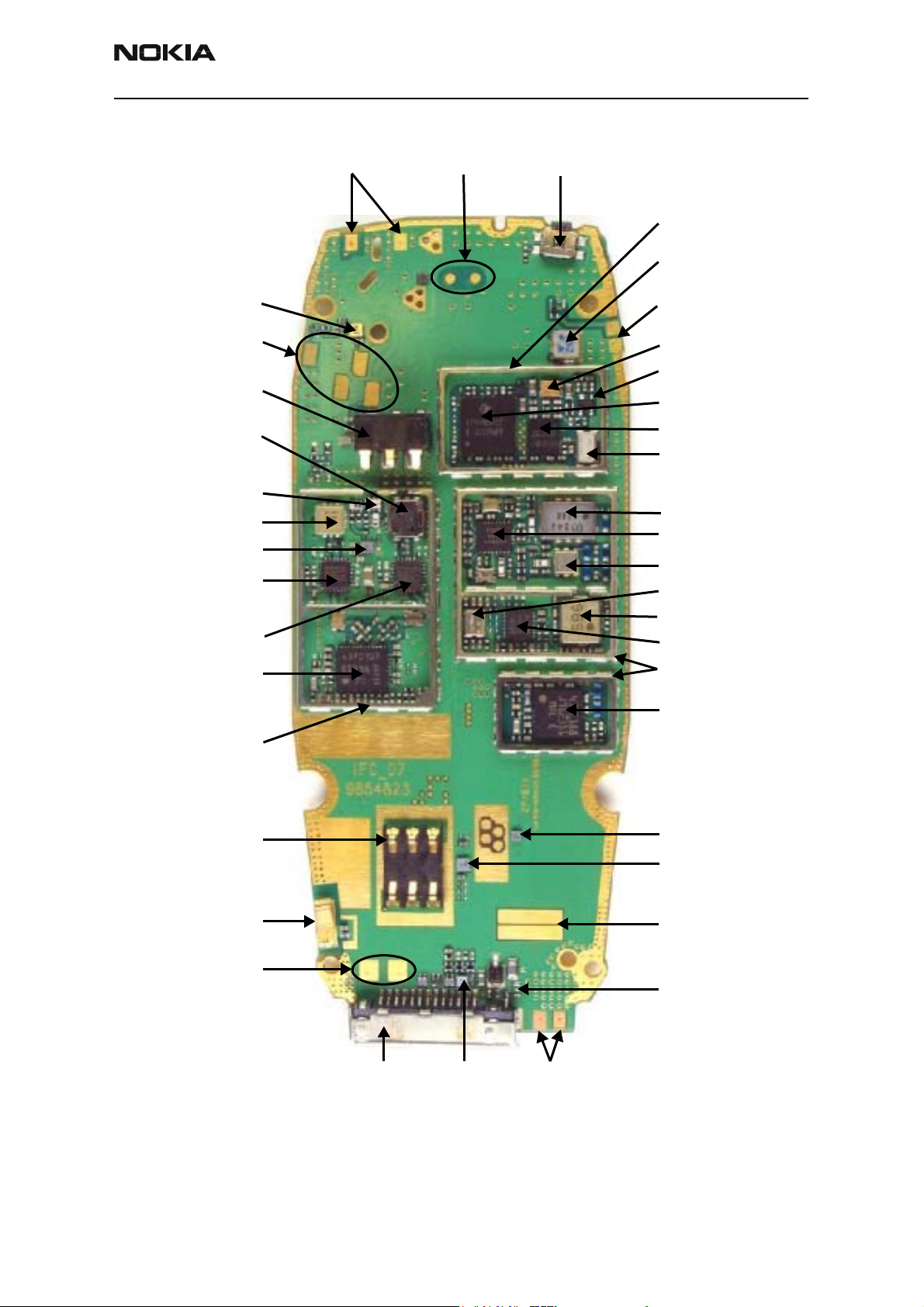
Phone Components
Figures 1 and 2 illustrate the main components of the 6015/6015i/6016i/6019i, and
6012.
Cell RF connector
GPS RF Connector
GND
VBATT
BSI
Flash
SRAM
UPP
BB Connector
UI LEDs
UEM
Figure 1: Component layout (bottom)
Page 6 ©2004 Nokia Corporation Company Confidential Issue 1 - Revision 002 09/2004
Page 7
6015/6015i/6016i/6019i (RH-55), 6012 (RM-20)
Nokia Customer Care Troubleshooting - RF
Audio ASIP
HS jack pads
Battery connector
PCS duplexer
Diplexer
Cell duplexer
PWR detector
Cell PW amp
Cell antenna pads HF speaker pads
Power switch
GPS shield
GPS CER filter
GPS antenna pads
GPS SAW filter
GPS LNA
GPS BB IC
GPS RF IC
GPS TCXO
SAW filter
LNA Alfred
SAW filter
VCTCXO
PCS PW amp
Jupiter RF TX
TX shield
RUIM connectors
Antenna
ground clip
Mic pads
UHF VCO
PLL synthesizer
RX shields
Batman RF RX
BI-DIR diode
ESD filter
Vibra pad
SM fuse
System
connector
diode
DC padsBI-DIR
Figure 2: Component layout (top)
Issue 1 - Revision 002 09/2004 ©2004 Nokia Corporation Company Confidential Page 7
Page 8

6015/6015i/6016i/6019i (RH-55), 6012 (RM-20)
Troubleshooting - RF Nokia Customer Care
General Troubleshooting
Use the following steps to troubleshoot some common issues, such as low transmitter
power, a faulty receiver, or a phone that cannot make a call.
TX Power Low
If TX power is low, use Phoenix to turn on the transmitter in Local Mode and check the
following:
1. Perform a visual inspection of the PWB under a microscope to check for the
proper placement, rotation, and soldering of components.
2. Look for the presence of a CDMA modulated signal on a spectrum analyzer at the
correct frequency.
• If a signal is present but off-frequency or distorted, check the synthesizer.
Most likely, one of the synthesizers is not locked or the VCO has no output
signal.
• If a signal is not present, or present but low in amplitude, use check the
probing diagrams to determine where in the chain the fault occurs.
3. Check that the AGC PDMs are set for the desired TX power and ensure the AGC
voltages are correct.
4. Check the synthesizers for proper frequency and amplitude.
5. Ensure that the power supplies to the transmitter have the correct voltage.
Receiver Not Working Properly
If the receiver is not working properly, turn it on in Local Mode and check the following:
1. Turn on receiver with Phoenix and inject a signal.
2. Check the AGC PDM.
3. Perform a visual inspection of the PWB under a microscope to check for the
proper placement, rotation, and soldering of components.
4. Measure signal levels at various points in the chain and determine where in the
chain the fault lies.
5. Check the LOs for proper frequency and amplitude.
6. Ensure power supplies to receiver have correct voltage.
Phone Cannot Make a Call
Verify the following if the phone cannot make a call:
1. The phone is in Normal Mode (i.e., the phone is searching for a signal, net server
is on).
2. The Preferred Roaming List (PRL) is loaded into the phone.
3. The phone is tuned and has passed tuning. (Read the tuning parameters using the
batch tune component in Phoenix; an untuned phone has all zeros in the tuning
file.)
Page 8 ©2004 Nokia Corporation Company Confidential Issue 1 - Revision 002 09/2004
Page 9
6015/6015i/6016i/6019i (RH-55), 6012 (RM-20)
Nokia Customer Care Troubleshooting - RF
4. The call box channel is set for a channel in PRL.
5. The SID is correct and entered into the phone.
6. The VCTCXO is centered as described in the VCTCXO tuning description on
page 49.
7. The transmitter and receiver are working properly in Local Mode.
Transmitter Parts
Following are the transmitter RF parts.
PCS PAPCS duplexer
PCS
coupler
PCS TX SAW filter
Diplexer
Cell
coupler
Cell
duplexer
Power detector
Cell PA
Figure 3: Transmitter parts
Cell TX SAW filter Jupiter TX IC
Issue 1 - Revision 002 09/2004 ©2004 Nokia Corporation Company Confidential Page 9
Page 10
6015/6015i/6016i/6019i (RH-55), 6012 (RM-20)
Troubleshooting - RF Nokia Customer Care
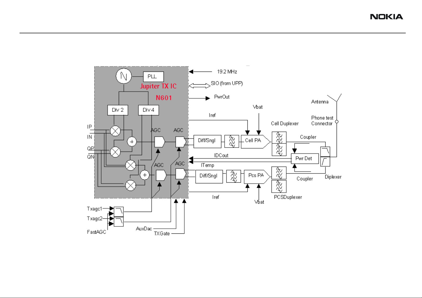
Cell Transmitter Block Diagram
Following is the block diagram for the TX system.
Figure 4: TX system block diagram
Page 10 ©2004 Nokia Corporation Company Confidential Issue 1 - Revision 002 09/2004
Page 11
6015/6015i/6016i/6019i (RH-55), 6012 (RM-20)
Nokia Customer Care Troubleshooting - RF
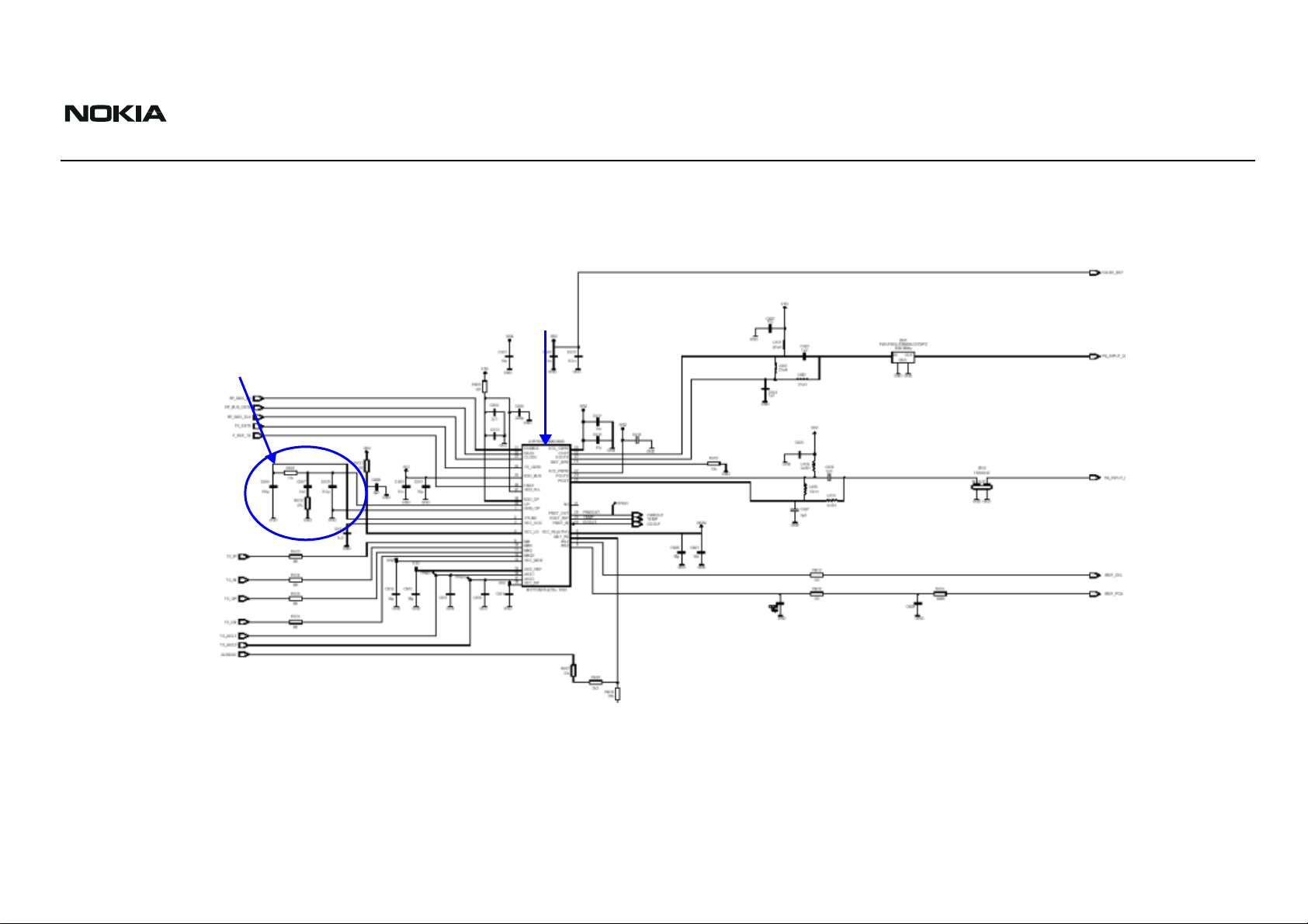
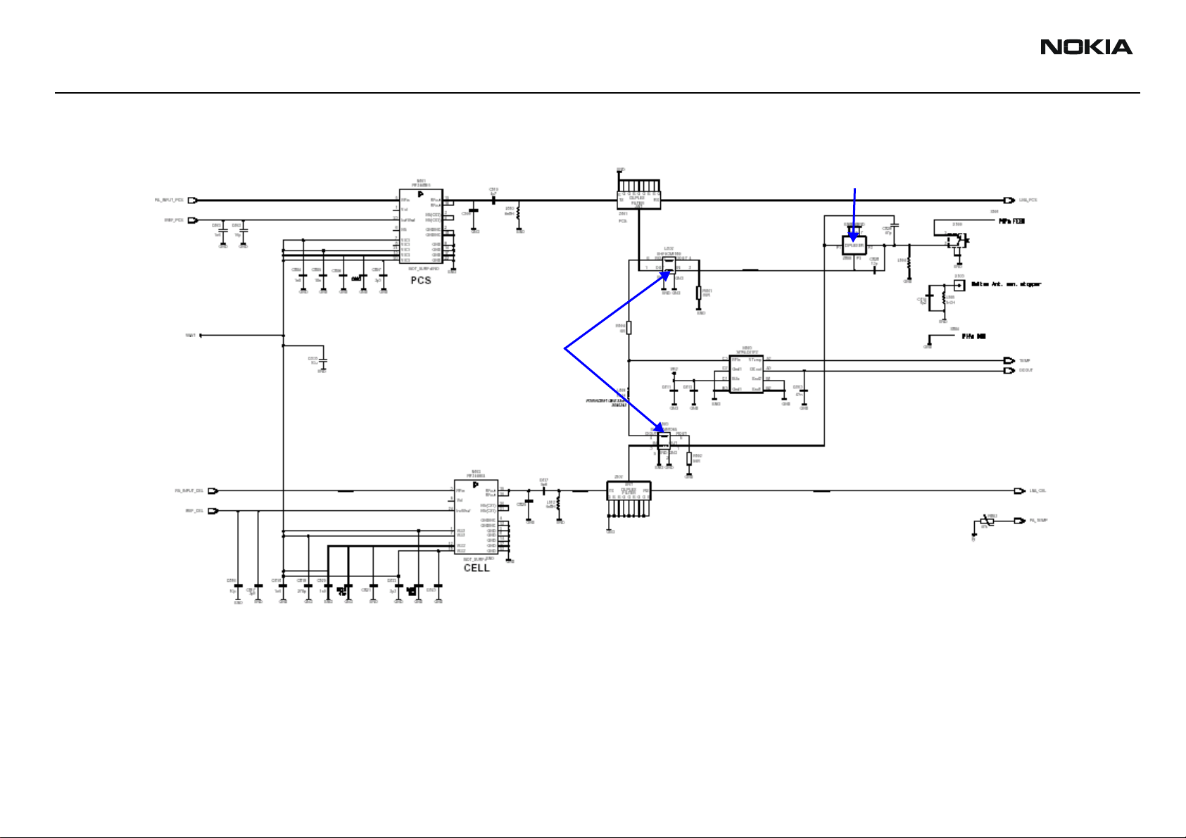
Transmitter Schematics
The following schematics are for general reference only. See the Schematics chapter for detailed versions.
Jupiter TX IC
TX LO lock voltage
Cell TX filter
PCS TX filter
Loop filter
Figure 5: Transmitter schematic 1
Issue 1 - Revision 002 09/2004 ©2004 Nokia Corporation Company Confidential Page 11
Page 12
6015/6015i/6016i/6019i (RH-55), 6012 (RM-20)
Troubleshooting - RF Nokia Customer Care
PCS PA
PCS duplexer
Diplexer
Power detector
Couplers
Cell PA
Cell duplexer
Figure 6: Transmitter schematic 2
Page 12 ©2004 Nokia Corporation Company Confidential Issue 1 - Revision 002 09/2004
Page 13
6015/6015i/6016i/6019i (RH-55), 6012 (RM-20)
Nokia Customer Care Troubleshooting - RF
Transmitter Troubleshooting Setup
Use the following sections to set up troubleshooting in Phoenix according to the band
you are using:
• "AMPS TX Setup"
• "Cell TX Setup"
• "PCS TX Setup"
AMPS TX Setup
Use the following procedures to prepare for AMPS TX troubleshooting using Phoenix.
1. Connect RF test connector to a call box.
2. Connect the phone to a PC via the bottom connector, and connect a power
supply.
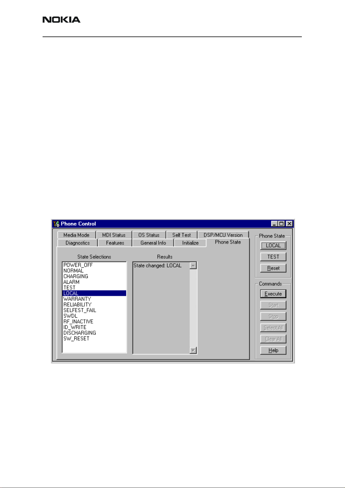
3. Open the Troubleshooting menu, and click Phone Control.
The Phone Control dialog box appears.
4. On the Phone Control dialog box, click the LOCAL button in the Phone State
area to put the phone into Local Mode.
Figure 7: Phone Control dialog box
5. Open the Troubleshooting menu, point to AMPS, and click AMPS Control.
Issue 1 - Revision 002 09/2004 ©2004 Nokia Corporation Company Confidential Page 13
Page 14
6015/6015i/6016i/6019i (RH-55), 6012 (RM-20)
Troubleshooting - RF Nokia Customer Care
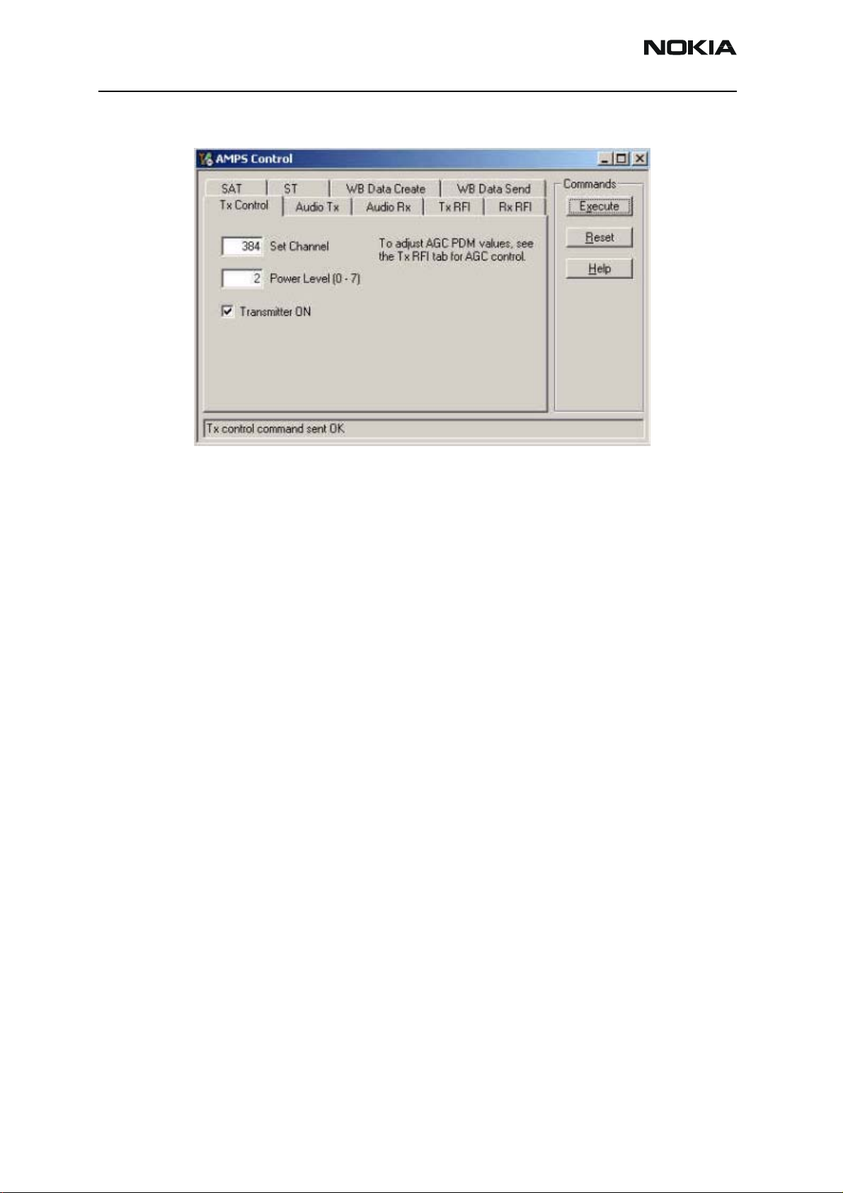
The AMPS Control dialog box appears.
6. Click the Tx Control tab.
7. In the Set Channel field, type 384.
8. In the Power Level field, type 2.
9. Select the Transmitter ON option, and click Execute.
10. Configure the spectrum analyzer using the following values:
Cell TX Setup
Use the following procedures to prepare for Cell TX troubleshooting using Phoenix.
1. On the Phone Control dialog box, click the LOCAL button in the Phone State
Figure 8: AMPS Control dialog box
• Center Frequency = 836.52 MHz
• Span = 100 MHz
• Amplitude = 20 dBm
• Attenuation = Auto
• BW = Auto
area to put the phone into Local Mode. (See Figure 7 on page 13.)
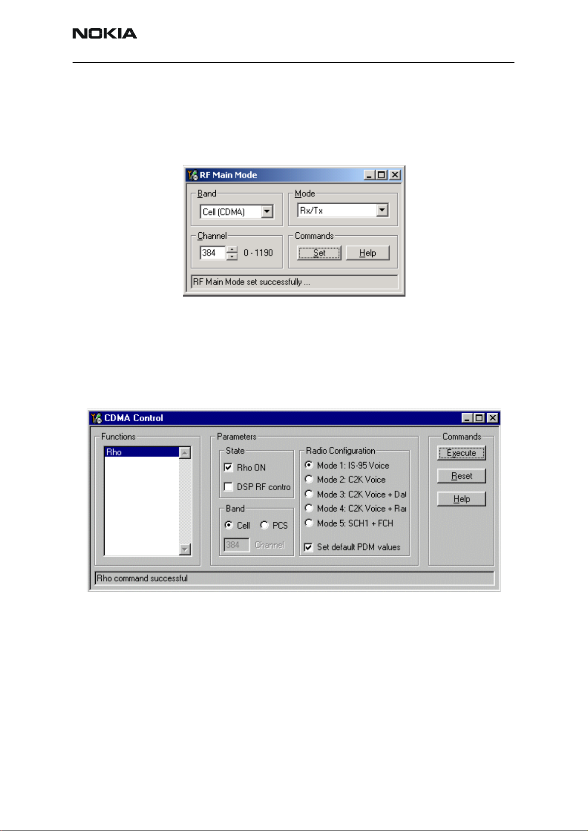
2. Open the Troubleshooting menu, point to RF, and click RF Main Mode.
The RF Main Mode dialog box appears.
Page 14 ©2004 Nokia Corporation Company Confidential Issue 1 - Revision 002 09/2004
Page 15
6015/6015i/6016i/6019i (RH-55), 6012 (RM-20)
Nokia Customer Care Troubleshooting - RF
3. Select the following values on the RF Main Mode dialog box:
• Band = Cell (CDMA)
• Channel = 384
• Mode = Rx/Tx
Figure 9: RF Main Mode dialog box
4. Click Set.
Note: Be sure that the “RF Main Mode set successfully” message appears in the status bar.
5. Open the Troubleshooting menu, point to RF, and click CDMA Control.
The CDMA Control dialog box appears.
Figure 10: CDMA Control dialog box for Cell TX troubleshooting
6. Select the following values on the CDMA Control dialog box.
• State = Rho ON
• Band = Cell
• Radio Configuration = Mode 1: IS-95 Voice
• Select the Set default PDM values check box.
7. Click Execute.
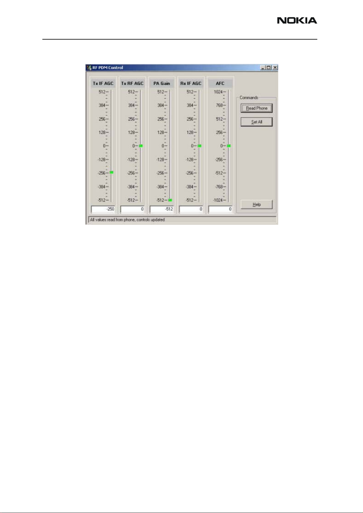
8. Open the Troubleshooting menu, point to RF, and click PDM Control.
Issue 1 - Revision 002 09/2004 ©2004 Nokia Corporation Company Confidential Page 15
Page 16
6015/6015i/6016i/6019i (RH-55), 6012 (RM-20)
Troubleshooting - RF Nokia Customer Care
The RF PDM Control dialog box appears.
9. Click Read Phone to update the values.
10. Configure the spectrum analyzer using the following values:
PCS TX Setup
Use the following procedures to prepare for PCS TX troubleshooting using Phoenix.
1. Open the Troubleshooting menu, and point to Phone Control.
2. Click the LOCAL button in the Phone State area to put the phone into Local
3. Open the Troubleshooting menu, point to RF, and click RF Main Mode.
Figure 11: RF PDM Control dialog box for Cell troubleshooting
• Center Frequency = 836.52 MHz
• Span = 100 MHz
• Amplitude = 20 dBm
• Attenuation = Auto
• BW = Auto
The Phone Control dialog box appears.
Mode. (See Figure 7 on page 13.)
The RF Main Mode dialog box appears. (See Figure 9 on page 15.)
Page 16 ©2004 Nokia Corporation Company Confidential Issue 1 - Revision 002 09/2004
Page 17

6015/6015i/6016i/6019i (RH-55), 6012 (RM-20)
Nokia Customer Care Troubleshooting - RF
4. Select the following values on the RF Main Mode dialog box:
• Band = PCS (CDMA)
• Channel = 600
• Mode = Rx/Tx
5. Click Set.
Note: Be sure that the “RF Main Mode set successfully” message appears in the status bar.
6. Open the Troubleshooting menu, point to RF, and click CDMA Control.
The CDMA Control dialog box appears. (See Figure 10 on page 15.)
7. Select the following values on the CDMA Control dialog box.
• State = Rho ON
• Band = PCS
• Radio Configuration = Mode 1: IS-95 Voice
• Select the Set default PDM values check box.
8. Click Execute.
9. Open the Troubleshooting menu, point to RF, and click PDM Control.
The RF PDM Control dialog box appears. (See Figure 11 on page 16.)
10. Click Read Phone to update the values.
11. Configure the spectrum analyzer using the following values:
• Center Frequency = 1880 MHz
• Span = 100 MHz
• Amplitude = 20 dBm
• Attenuation = Auto
• BW = Auto
Transmitter Troubleshooting
After Phoenix is set up using either the AMPS, Cell, or PCS setup procedures, use the
following steps to troubleshoot the transmitter.
1. Use a voltmeter to verify that the VR2, VR6, and VR1B are on the transmit
system. (See Figure 13 on page 19 and Figure 14 on page 20).
• If any are missing, look for SMD problems around Jupiter and the UEM.
• If the SMD is good, replace the UEM.
Issue 1 - Revision 002 09/2004 ©2004 Nokia Corporation Company Confidential Page 17
Page 18

6015/6015i/6016i/6019i (RH-55), 6012 (RM-20)
Troubleshooting - RF Nokia Customer Care
2. If all DC voltages are present, check the AGC control voltages. (See Figure 13 on
page 19).
• If the voltages are incorrect, check the SMDs around the TX_AGC1 and
TX_AGC2 lines.
• If SMDs are all good, replace the UPP.
3. Using an oscilloscope, look at the input modulation waveforms on R603, R604,
R605, and R606. They should all be present with an AC swing of about 500 mVpp
and a +1.2 V offset.
• If one or more waveforms are missing, look for SMD problems around these
resistors.
• If the SMD is good, replace the UEM.
4. Probe the Cell TX output of Jupiter using AAS-10 type RF probe.
5. Use the spectrum analyzer to probe the RF center frequency (see the "AMPS TX
Setup", "Cell TX Setup", or "PCS TX Setup" section for the correct spectrum
analyzer settings).
• If there is no RF or low RF, look for faulty SMD around the Jupiter chip.
• If the SMD is good, replace the Jupiter chip.
6. Probe the PA input. If level is low, look for an SMD issue on the TX filter. Reflow
or replace the filter as necessary.
7. Probe the PA output. If the RF is missing or low, look for Vbatt voltages and SMD
issues on and around the PA. If these voltages are good, replace the PA.
8. Probe the duplexer output. If the RF is missing or low, reflow or replace the
duplexer.
9. Probe the coupler output. If the RF is missing or low, reflow or replace the
coupler.
10. Probe the diplexer output. If the RF is missing or low, reflow or replace the
diplexer.
Failed Test: TX PA Detector
1. Use Phoenix to set the phone in Local Mode, and activate the TX with default
output power. The output power at the RF test connector should read
9 dBm +/- 4 dB.
2. Use a voltmeter on DC, and probe the detector output at C813. The voltmeter
should read approximately 1.4 V. If not, replace the detector (N803).
See Figure 13 on page 19 for test point location and common power and voltage
variations.
Page 18 ©2004 Nokia Corporation Company Confidential Issue 1 - Revision 002 09/2004
Page 19
6015/6015i/6016i/6019i (RH-55), 6012 (RM-20)
Nokia Customer Care Troubleshooting - RF
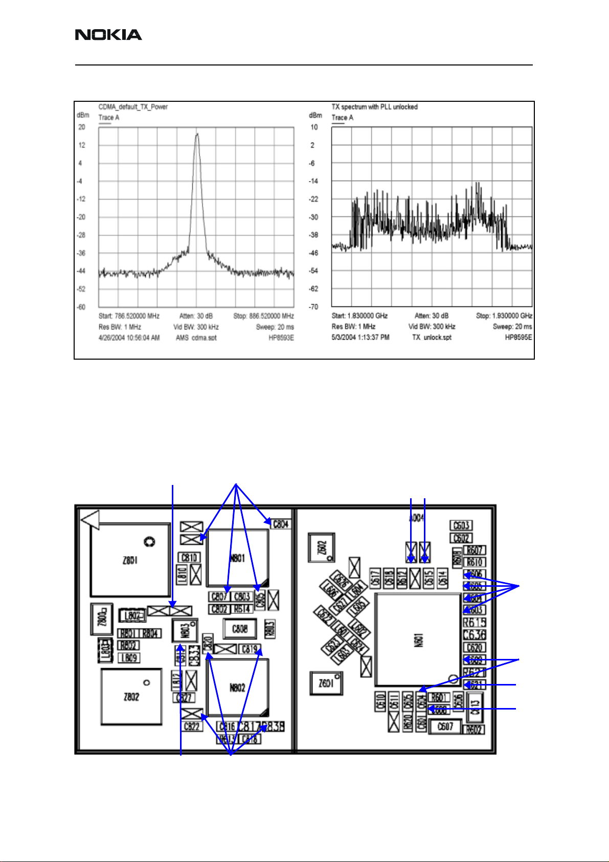
Good output
Figure 12: The output of the phone on a spectrum analyzer should look like the figure on the left
Bad output
If using the AAS-10 probe with the phone connected to the call box, the amplitude
should be approximately -7 dBm at the antenna test point on the top of the PWB.
TX DC Probe Points
Following are the transmitter DC probe points on the top side of the PWB. See Table 1 on
page 20 for test point descriptions and values.
1
2
4
3
5
6
7
8
10 9
Figure 13: Top side TX DC test points
Issue 1 - Revision 002 09/2004 ©2004 Nokia Corporation Company Confidential Page 19
Page 20

6015/6015i/6016i/6019i (RH-55), 6012 (RM-20)
Troubleshooting - RF Nokia Customer Care
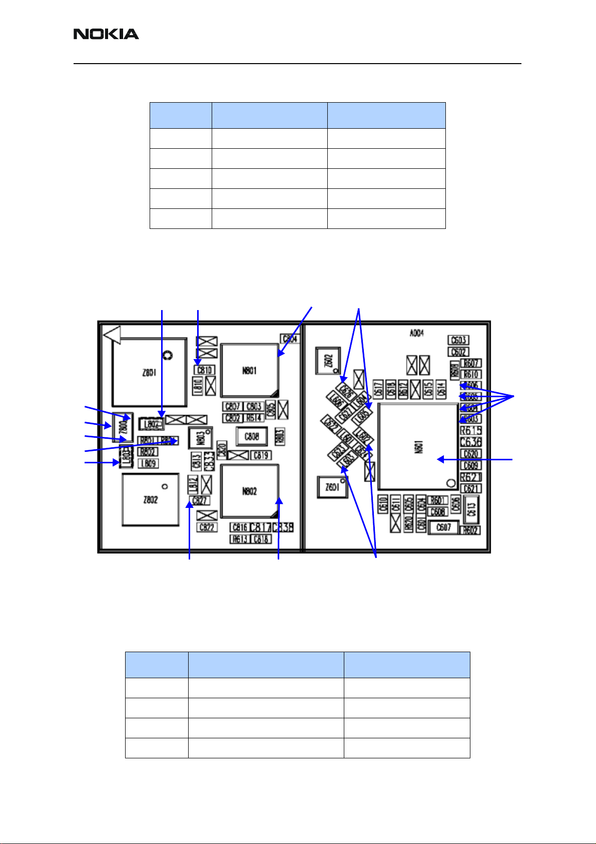
11
16
12
13
Figure 14: Bottom side TX DC probe points
14
15
Table 1 shows the TX DC probe points for the bottom and top sides of the PWB.
Table 1: TX DC Probe Points
Test Point Description Value
1 Power detector VR2 2.76V
2 Vbatt PCS*
3 AGC 2 0.1 to 1.8V
4 AGC 1 0.1 to 1.8V
5 TX IQ IN
TX IQ IN with oscilloscope
6VR6 2.8V
7VR1B 4.8V
8 TX UHF LO lock voltage 1.2V
9 Vbatt Cell*
10 Power detector output PCS:
11 V re fR F 1 1 .4 5 V
Approximately 1. 2V
Approximately 500 mV p-p
1.9V at <5dBm
1.6V at 15dBm
0.8V at 25dBm
Cell:
1.9V at <5dBm
1.7V at 15dBm
1.3V at 25dBm
Page 20 ©2004 Nokia Corporation Company Confidential Issue 1 - Revision 002 09/2004
Page 21
6015/6015i/6016i/6019i (RH-55), 6012 (RM-20)
Nokia Customer Care Troubleshooting - RF
Table 1: TX DC Probe Points (Continued)
Test Point Description Value
12 VR6 2.78V
13 VR1B 4.7V
14 VR2 2.78V
15 Vbatt* 3.2 to 4.7V
16 TX detector out Approximately 1.5V
Note: Vbatt also appears at the outputs of the PAs.
TX RF Probe Points
Following are the TX RF probe points.
21
3
4
14
13
12
11
10
89
Figure 15: TX RF test points
7
Table 2 includes the values from the test points in Figure 15. The PCS frequency is at
1880 MHz, and the Cell/AMPS frequency is at 836.25 MHz.
Table 2: TX RF Probe Points
Test Point Description Value
5
6
1 PCS duplexer out -2 dBm
2 PCS PA out -2 dBm
3 PCS PA in -23 dBm
4 PCS Jupiter out -22 dBm
Issue 1 - Revision 002 09/2004 ©2004 Nokia Corporation Company Confidential Page 21
Page 22

6015/6015i/6016i/6019i (RH-55), 6012 (RM-20)
Troubleshooting - RF Nokia Customer Care
Table 2: TX RF Probe Points (Continued)
Test Point Description Value
5 TX IQ in with oscilloscope Approximately 500 mV p-p
with +1.2 V offset
6 TX UHF LO PCS: 3760 MHz, -54 dBm
Cell: 3346.08 MHz, -57 dBm
7 Jupiter out Cell: -15 dBm
AMPS: -6 dBm
8 PA in Cell: -15 dBm
AMPS: -7 dBm
9 PA out Cell: +11 dBm
AMPS: +22 dBm
10 Duplexer out Cell: +10 dBm
AMPS: +20 dBm
11 Power detector in PCS: -17 dBm
12 Coupler out Cell: +8 dBm
13 Diplexer out PCS: -2 dBm
14 PCS coupler out -1 dBm
Receiver Troubleshooting
The primary component of the receiver is the Alfred Rx IC. This Rx IC contains two LNAs
and mixers. The other components are passive. There are two RF SAW filters for the Cell
and PCS bands. In addition, there are two IF filters, an IF SAW for CDMA and an IC
Crystal for AMPS. The back-end of the receiver consists of the Batman IC. The VGA and
IQ demodulator are the main functions.
Following is the RX system block diagram.
Cell: -8 dBm
AMPS: +3 dBm
AMPS: +18 dBm
Cell: +10 dBm
AMPS: +19 dBm
Page 22 ©2004 Nokia Corporation Company Confidential Issue 1 - Revision 002 09/2004
Page 23

6015/6015i/6016i/6019i (RH-55), 6012 (RM-20)
Nokia Customer Care Troubleshooting - RF
PCS RF FILTER
PCS DUPLEX FILTER
DIPLEX FILTER
CELL DUPLEX FILTER
UHF
VCO
PCS
LNA
Alfred Rx IC Batman Rx Down-converter
Cell
LNA
CELL RF FILTER
LOA
PCS
RFA
Cell
RFA
AMPS
CDMA
Figure 16: Receiver system block diagram
AMPS
IF
FILTER
CDMA
IF
FILTER
VGA
IQ
DEMOD
ADC
I
BBFIL/BBAMP
Q
Issue 1 - Revision 002 09/2004 ©2004 Nokia Corporation Company Confidential Page 23
Page 24

6015/6015i/6016i/6019i (RH-55), 6012 (RM-20)
Troubleshooting - RF Nokia Customer Care
Receiver Schematics
The following schematics are for general reference only. See the Schematics chapter for detailed versions.
Cell RF SAW filter
PC RF SAW filter
AMPS IF crystal filter
Alfred RX
front-end IC
Figure 17: Receiver schematic 1
CDMA IF SAW filter
Page 24 ©2004 Nokia Corporation Company Confidential Issue 1 - Revision 002 09/2004
Page 25

6015/6015i/6016i/6019i (RH-55), 6012 (RM-20)
Nokia Customer Care Troubleshooting - RF
Loop filter
RX LO lock voltage
1.2 to 1.7 Vdc
Batman RX downconverter
Figure 18: Receiver schematic 2
Issue 1 - Revision 002 09/2004 ©2004 Nokia Corporation Company Confidential Page 25
Page 26

6015/6015i/6016i/6019i (RH-55), 6012 (RM-20)
Troubleshooting - RF Nokia Customer Care
RF AGC Status
Figure 19 shows the RF AGC Status dialog box. When configuring the values on this
dialog box, note the following:
• The RF AGC status functionality only works in Call Mode.
•In the PLL Lock Status area, bright green indicates a locked PLL and dark green
indicates an unlocked PLL.
•In the Baseband Type field, ensure that the correct baseband is selected (BB 4.0).
• Clicking the Update Once Per Second button allows you to toggle between the
Update Once Per Second and Stop Updating functions.
AFC PDM settings
LNA Gain (High[Boost for PCS]/Low)
PA AGC PDM settings
Figure 19: RF AGC Status dialog box
RX IF AGC PDM settings
TX AGC 2 PDM settings
BBAMP Gain Settings
TX AGC 1 PDM settings
Page 26 ©2004 Nokia Corporation Company Confidential Issue 1 - Revision 002 09/2004
Page 27

6015/6015i/6016i/6019i (RH-55), 6012 (RM-20)
Nokia Customer Care Troubleshooting - RF
Turning on the RX Path
Use the following steps to turn on the RX path using Phoenix.
1. Turn on Receiver Only in CDMA mode.
2. On the Phone Control dialog box, click the LOCAL button in the Phone State
area to put the phone into Local Mode.
Figure 20: Phone Control dialog box
3. Click Execute.
4. Depending on the mode of phone you have, use the settings from Table 3 on the
RF Main Mode dialog box.
Table 3: RF Main Mode Dialog Box Settings
Band Mode Channel
Cell RX = 881.52 MHz 384
AMPS RX = 881.52 MHz 384
PCS RX = 1960 MHz 600
Issue 1 - Revision 002 09/2004 ©2004 Nokia Corporation Company Confidential Page 27
Page 28

6015/6015i/6016i/6019i (RH-55), 6012 (RM-20)
Troubleshooting - RF Nokia Customer Care
Figure 21: RF Main Mode dialog box for Cell (top), AMPS (middle), and PCS (bottom)
Page 28 ©2004 Nokia Corporation Company Confidential Issue 1 - Revision 002 09/2004
Page 29

6015/6015i/6016i/6019i (RH-55), 6012 (RM-20)
Nokia Customer Care Troubleshooting - RF
Switching the RX Gain States
Use the RF Gen I/O dialog box to switch the gain state (Hi and Lo) for CDMA and AMPS
modes. Select the desired state, and click Refresh.
High Gain State (default)
Cell
AMPS
Low Gain State
PCS
Figure 22: RF Gen I/O dialog box
Cell Receiver Check from RF to IQ
Use the following values to check the CDMA Cell RX functionality from RF to IQ output.
1. Start Phoenix in Local Mode with only the RX path turned on.
2. Inject a –75dBm CW signal of 881.82MHz (i.e. 300kHz offset from 881.52MHz or
10 channels away).
3. Measure a 300kHz tuning on the analyzer. You should see a typical -21dBm IQ
tuning for CDMA Cell.
CDMA
Issue 1 - Revision 002 09/2004 ©2004 Nokia Corporation Company Confidential Page 29
Page 30

6015/6015i/6016i/6019i (RH-55), 6012 (RM-20)
m
Troubleshooting - RF Nokia Customer Care
Cell I Q Output
dBm
0
-10
-20
-30
-40
-50
-60
-70
-80
Trace A
1
Trace A
302 kHz
1
-21.2500 dB
-90
-100
Centre: 300 kHz Span: 200 kHzAtten: 10 dB
Res BW: 3 kHz Vid BW: 3 kHz Sweep: 100 ms
5/5/2004 3:29:30 PM HP8595ECellIQ.spt
Figure 23: Receiver IQ level on CDMA Cell band
Figure 24 shows the Cell spectrum with an inject tone at -75dBm, as well as the IQ
output test points. Note that DC is present on the IQ output test points, and all test
points should be approximately equal.
RX_IP RX_QPRX_IN RX_QN
Figure 24: Cell spectrum (left) and IQ output test points (right)
Page 30 ©2004 Nokia Corporation Company Confidential Issue 1 - Revision 002 09/2004
Page 31

6015/6015i/6016i/6019i (RH-55), 6012 (RM-20)
m
Nokia Customer Care Troubleshooting - RF
PCS Receiver Check from RF to IQ
Use the following values to check the PCS receiver functionality from RF to IQ output.
1. Start Phoenix in Local Mode with only the RX path turned on.
2. Inject a –75dBm CW signal of 1960.5MHz (i.e. 500kHz offset from 1960MHz or
10 channels away).
3. Measure a 500kHz tuning on the analyzer. You should see a typical -22dBm IQ
tuning. If the 300kHz tone works but the 500kHz tone does not, it is possible that
the BB filter was not set by Phoenix.
PCS I Q Output
dBm
0
-10
-20
-30
Trace A
2
Trace A
503 kHz
-22.4500 dB
2
-40
-50
-60
-70
-80
-90
-100
Centre: 500 kHz Span: 200 kHzAtten: 10 dB
Res BW: 3 kHz Vid BW: 3 kHz Sweep: 100 ms
5/5/2004 3:37:55 PM HP8595EPcsIQ.spt
Figure 25: Receiver IQ Level on PCS Band
Figure 25 shows the PCS spectrum with an inject tone at -75dBm, as well as the IQ
output test points. Note that DC is present on the IQ output test points, and all test
points should be approximately equal.
Issue 1 - Revision 002 09/2004 ©2004 Nokia Corporation Company Confidential Page 31
Page 32

6015/6015i/6016i/6019i (RH-55), 6012 (RM-20)
Troubleshooting - RF Nokia Customer Care
RX_IP RX_QPRX_IN RX_QN
Figure 26: Cell spectrum (left) and IQ output test points (right)
AMPS Receiver Check from RF to IQ
Use the following steps to check the AMPS receiver functionality from RF to IQ output.
1. Start Phoenix in Local Mode with only the RX path turned on.
2. Inject a –75dBm CW signal of 881.53MHz (i.e., 10kHz offset from 881.52MHz)
into the RF.
3. Measure a 10kHz tone on the analyzer. You should see a typical -20Bm IQ
tuning for AMPS.
Page 32 ©2004 Nokia Corporation Company Confidential Issue 1 - Revision 002 09/2004
Page 33

6015/6015i/6016i/6019i (RH-55), 6012 (RM-20)
Nokia Customer Care Troubleshooting - RF
Figure 27: Receiver IQ Level on AMPS band
Figure 28 shows the AMPS spectrum with an inject tone at -75dBm, as well as the IQ
output test points. Note that DC is present on the IQ output test points, and all test
points should be approximately equal.
RX_IP RX_QPRX_IN RX_QN
Figure 28: AMPS spectrum (left) and IQ output test points (right)
Issue 1 - Revision 002 09/2004 ©2004 Nokia Corporation Company Confidential Page 33
Page 34

6015/6015i/6016i/6019i (RH-55), 6012 (RM-20)
Troubleshooting - RF Nokia Customer Care
Receiver Diagnostic Signal Tracing
Use the following steps to trace a receiver signal.
1. Inject an external signal source of –25dBm into the RF input. An Agilent call box
8960 is recommended.
2. Press the Call Setup button, press the Active Cell soft button, and select CW.
3. Inject a CW signal for PCS (1960MHz) or Cell/AMPS (881.52MHz) at a fixed
–25dBm power level.
Receiver IF RF
The test point measurements were taken using an AAS-10 probe. Signal levels are
approximate, and accuracy may be +/- 2dB or more, depending on the position of the
grounding probe.
CDMA IF
SAW filter
Alfred
RX FE IC
PCS RF
SAW filter
AMPS IF
crystal filter
1
7
6
Cell RF
5
4
Figure 29: Receiver RF troubleshooting test points
2
SAW filter
3
Page 34 ©2004 Nokia Corporation Company Confidential Issue 1 - Revision 002 09/2004
Page 35

6015/6015i/6016i/6019i (RH-55), 6012 (RM-20)
Nokia Customer Care Troubleshooting - RF
Table 4 includes the descriptions and values for the RX RF troubleshooting test points
shown in Figure 29.
Table 4: Receiver RF Troubleshooting Values
Receiver IF
Test
Point
1 RX LO (from VCO) 1009.62MHz at -8 dBm
2 Cell Channel 384 (from duplexer) 881.52MHz at -31 dBm
3 Cell Channel 384 (to RF SAW) 881.52MHz at -20 dBm (HG)
4 PCS Channel 600 (from duplexer) 1960MHz at -40 dBm
5 PCS Channel 600 (to RF SAW) 1960MHz at -30 dBm (HG)
6 IF MIX OUT (from Alfred) 128.1MHz at -20 dBm (HG)
7 IFA IN (to Alfred) 128.1MHz at -15 dBm (HG)
Description Value
2088.1MHz at -14 dBm
881.52MHz at -36 dBm (LG)
1960MHz at -45 dBm (LG)
128.1MHz at -37 dBm (LG)
128.1MHz at -30 dBm (LG)
2
5
6
1
Figure 30: Receiver IF troubleshooting test points
4
3
7
Issue 1 - Revision 002 09/2004 ©2004 Nokia Corporation Company Confidential Page 35
Page 36

6015/6015i/6016i/6019i (RH-55), 6012 (RM-20)
Troubleshooting - RF Nokia Customer Care
Table 5 includes the descriptions and values for RX IF troubleshooting test points shown
in Figure 30.
Table 5: Receiver IF Troubleshooting Values
Test
Point
1 CDMA IF (to SAW) 128.1 MHz Cell Channel 384 at -6 dBm (HG)
2 CDMA_IF_P (to Batman) 128.1 MHz Cell -18 dBm (HG)
3 AMPS IF (to MCF) 128.1MHz Cell Channel 384 at -17 dBm (HG)
4 AMPS_IF_N (to Batman) 128.1MHz Cell -23 dBm (HG)
5 CDMA_IF_N (to Batman) 128.1 MHz Cell -18 dBm (HG)
6 AMPS_IF_P (to Batman) 128.1MHz Cell -23 dBm (HG)
Description Value
Cell Channel 384 at -23 dBm (LG)
PCS Channel 600 at -6 dBm (HG)
PCS Channel 600 at -20 dBm (LG)
Cell -35 dBm (LG)
PCS -18 dBm (HG)
PCS -32 dBm (LG)
Cell Channel 384 at -34 dBm (LG)
Cell -41 dBm (LG)
Cell -35 dBm (LG)
PCS -18 dBm (HG)
PCS -32 dBm (LG)
Cell -41 dBm (LG)
7 RX LO 256.2 MHz; -60 dBm
Page 36 ©2004 Nokia Corporation Company Confidential Issue 1 - Revision 002 09/2004
Page 37

6015/6015i/6016i/6019i (RH-55), 6012 (RM-20)
Nokia Customer Care Troubleshooting - RF
Receiver DC
1
5
Alfred RX FE IC
4
Figure 31: Receiver DC troubleshooting test points and RX front-end logic levels
6
2
7 8
3
Table 6 includes the descriptions and values for RX DC troubleshooting test points shown
in Figure 31.
Table 6: Receiver DC Troubleshooting Values
Test
Point
1 LO Vdd 2.59 VDC LO Amp Vdd supply lines for Cell and PCS
Description Value
2 RFA Vdd 2.76 VDC RF Amp Vdd supply line for Cell band
3 C_LNA Vdd 2.76 VDC External Vdd supply line for Cell LNA
4 P_LNA Vdd 2.76 VDC External Vdd supply line for PCS LNA
5 IFA Vdd 2.76 VDC IF Amp Vdd supply line for CDMA and AMPS IFs
6 IFA Vdd 2.76 VDC IF Amp Vdd supply line for CDMA and AMPS IFs
7 RX LO Lock Voltage 1.2 to 1.7 VDC
8 RX LO 256.2 MHz -60 dBm
Issue 1 - Revision 002 09/2004 ©2004 Nokia Corporation Company Confidential Page 37
Page 38

6015/6015i/6016i/6019i (RH-55), 6012 (RM-20)
Troubleshooting - RF Nokia Customer Care
Receiver Logic Input Voltages
Following are the measure logic levels for the RX front end (N750). See Figure 22 on
page 29 for the manual selection of logic states using Phoenix.
2
31
Table 7 includes the logic level values for the RX front end.
Table 7: RX Front-end (N750) Logic Levels
Logic Input Voltages
Mode
IF_SEL BAND GAIN_CTL
Cell CDMA High Gain 0 V 0.1 V 2.75 V
Cell CDMA Low Gain 0 V 0.1 V 0 V
PCS CDMA High Gain 0 V 2.68 V 2.75 V
PCS CDMA Low Gain 0 V 2.68 V 0 V
AMPS High Gain 2.76 V 0.1 V 2.76 V
AMPS Low Gain 2.76 V 0.1 V 0 V
If the logic levels are significantly off (+/- 0.2 V), replace Alfred (N750) and re-measure.
If the voltages are still out of specifications, refer to the Baseband Troubleshooting
chapter.
Page 38 ©2004 Nokia Corporation Company Confidential Issue 1 - Revision 002 09/2004
Page 39

6015/6015i/6016i/6019i (RH-55), 6012 (RM-20)
Nokia Customer Care Troubleshooting - RF
Alfred (N750) Receiver Troubleshooting
Keep the following under consideration when troubleshooting the Alfred (N750) receiver:
• There is a separate LNA for 800MHz (Cell and AMPS) and 1900MHz (PCS).
• There is a separate RFA (inside Alfred) for 800MHz (Cell and AMPS) and
1900MHz (PCS).
• After the RFA, there is a mixer and then the signals are separated by CDMA (Cell
and PCS) and AMPS.
For example, if there is no IF frequency (128.1MHz) check both Cell and PCS. If
there is only one at 128.1MHz (L753), ensure that IF_SEL is working. If it is, then
replace Alfred because of a bad RFA.
If Cell and AMPS are working but PCS is not, look at the band select line and the
PCS RF filter before replacing Alfred.
Alfred DC Troubleshooting
There are two common explanations for an Alfred failure consisting of high current in
Local Mode with just the RX turned on:
Cell
IFAs
LO
Buffer
Figure 32: N750 (Alfred) receiver
RFA
PCS
RFA
Cell
LNA
PCS
LNA
• No presence of an LO signal
• Input impedance drop is shorting out one of the DC supply pins to the chip
Issue 1 - Revision 002 09/2004 ©2004 Nokia Corporation Company Confidential Page 39
Page 40

6015/6015i/6016i/6019i (RH-55), 6012 (RM-20)
Troubleshooting - RF Nokia Customer Care
IMPORTANT: You must check for both conditions before replacing Alfred. If you have
no LO signal, refer to "UHF Synthesizer Troubleshooting" on page 50. If you have a
significant supply voltage drop on one of the supply pins, then replace Alfred.
Table 8: Alfred Conditions and Supply Currents
Condition: Local Mode, Set
RX Only in RF Main Mode
Good phone 100mA
No UHF LO signal present 254mA
Pin 13 shorted 255mA
Synthesizer Troubleshooting
Faulty synthesizers can cause both RX and TX failures during tuning, in addition to the
VCTCXO tuning. However, it is recommended first to check for the presence of various LO
signals and their proper levels. The 19.2MHz reference clock is needed for the phone to
power up. Therefore, if everything fails, check for the presence of 19.2MHz. The level of
19.2MHz is also important because the UPP is very sensitive and can still pick up a very
weak 19.2MHz clock, which can result in the phone constantly resetting. See "19.2 MHZ
VCTCXO Reference Clock" on page 44 for more information.
The following synthesizers are used in the phone:
• Dual-band UHF:
• 1009.62 MHz for channel 384 in Cell and AMPS with separate LMX2310
PLL IC
Supply Current
(From Power Supply)
• 2088.1MHz for channel 600 in PCS with separate LMX2310 PLL IC
•TX UHF
• 3296.16 MHz ~ 3395.88 MHz for Cell and AMPS with PLL inside Jupiter IC
• 3700 MHz ~ 3819.9 MHz for PCS with PLL inside Jupiter IC
• RX VHF (256.2 MHz for Cell, AMPS, and PCS with PLL inside Batman IC
Incorrect PLL Frequencies
Following are possible causes for incorrect PLL frequencies:
• Incorrect power supplies to the PLL portion
• Control line to the VCO
• Loop filter or resonator components missing or incorrectly installed
• 19.2 MHz reference clock is missing or low
• Component failure (PLL IC, Batman, Jupiter, VCO, or VCTCXO)
Page 40 ©2004 Nokia Corporation Company Confidential Issue 1 - Revision 002 09/2004
Page 41

6015/6015i/6016i/6019i (RH-55), 6012 (RM-20)
Nokia Customer Care Troubleshooting - RF
Synthesizer Block Diagram
Batman
Batman
RX VHF Synthesizer
RX VHF Synthesizer
1
Phase
RF_BUS_CLK
RF_BUS_CLK
RF_BUS_DATA
RF_BUS_DATA
RF_BUS_EN1X
RF_BUS_EN1X
2
Reference
Reference
Divider
Divider
Reference
Reference
Divider
Divider
Phase
Detector
Detector
9-Bit B
9-Bit B
Counter
Counter
LMX2310U
LMX2310U
UHF Synthesizer
UHF Synthesizer
Phase
Phase
Detector
Detector
5-Bit A
5-Bit A
Counter
Counter
Charge
Charge
Pump
Pump
Charge
Charge
Pump
Pump
2 mA
2 mA
Prescaler
Prescaler
32/33
32/33
4 mA
4 mA
Band
Band
sel
sel
Tank
Tank
RX VHF VCO
RX VHF VCO
UHF VCO
UHF VCO
UHF RX LO
UHF RX LO
3
ALFRED
ALFRED
PCS_Cell
PCS_Cell
Prescaler
Phase
Phase
Detector
Detector
Charge
Charge
Charge
Charge
Pump
Pump
Pump
Pump
VDD BUS
VDD BUS
Prescaler
32/33
32/33
5-Bit A
5-Bit A
Counter
Counter
AutoCAL
AutoCAL
SYNTH_LE
SYNTH_LE
1
AFC
AFC
UEM
UEM
VCTCXO
VCTCXO
19.2 MHz
19.2 MHz
UPP
UPP
13-Bit B
13-Bit B
Counter
Counter
JUPITER D1
JUPITER D1
UHF Synthesizer
UHF Synthesizer
R
R
counter
counter
LD
LD
Serial Control Logic&Registers
Serial Control Logic&Registers
B counter
B counter
Figure 33: Synthesizer block diagram
Table 9 includes the component values shown in Figure 33.
VCO_CAL
VCO_CAL
Prescaler
Prescaler
Charge
Charge
Pump
Pump
A counter
A counter
VDD PLL
VDD PLL
AMPS
AMPS
CDMA
CDMA
4
Table 9: Synthesizer Block Diagram Component Values
Item Description Value
1 VCTCXO 19.2MHz
2 UHF LO 1009.62MHz (Cell channel 384)
2088.1MHz (PCS channel 600)
Issue 1 - Revision 002 09/2004 ©2004 Nokia Corporation Company Confidential Page 41
Page 42

6015/6015i/6016i/6019i (RH-55), 6012 (RM-20)
Troubleshooting - RF Nokia Customer Care
Table 9: Synthesizer Block Diagram Component Values (Continued)
Item Description Value
3 RX VHF LO 256.2MHz
4 TX UHF LO 3395.88MHz
3819.90MHz
Page 42 ©2004 Nokia Corporation Company Confidential Issue 1 - Revision 002 09/2004
Page 43

6015/6015i/6016i/6019i (RH-55), 6012 (RM-20)
Nokia Customer Care Troubleshooting - RF
Synthesizer Schematic
The following schematic is for general reference only. See the Schematics chapter for detailed versions.
VCTCXO with AFC control
19.2MHz buffer not installed
VCO
UHF PLL IC
Loop filter
Figure 34: Synthesizer schematic
Issue 1 - Revision 002 09/2004 ©2004 Nokia Corporation Company Confidential Page 43
Page 44

6015/6015i/6016i/6019i (RH-55), 6012 (RM-20)
Troubleshooting - RF Nokia Customer Care
Use the following steps to troubleshoot the synthesizer using Phoenix:
1. On the Phone Control dialog box, click the LOCAL button in the Phone State
area to put the phone into Local Mode.
Figure 35: Phone Control dialog box
2. Select the following values on the RF Main Mode dialog box:.
Table 10: RF Main Mode Dialog Box Settings
Synthesizer Band Mode Channel Notes
UHF
RX VHF RX One band is enough.
TX VHF Cell
Cell RX/TX 384 Allows for checking power to both RX and TX circuits.
PCS RX/TX 600
RX/TX 384
PCS
600
19.2 MHZ VCTCXO Reference Clock
The VCTCXO frequency is a 19.2MHz reference signal. Without 19.2MHz, the phone does
not power up. This signal goes to Batman, Jupiter, the UHF PLL, and also to the UPP. Use
a high impedance probe to check for the presence of the signal at the following points:
• F_REF_TX, clock reference to Jupiter, should be ~ -9 dBm
• F_REF_RX, clock reference to Batman, should be ~ -9 dBm
• CLK10M2_UPP, clock reference to UPP, should be ~ -9 dBm and ~2 dB less in the
other side on R517
Page 44 ©2004 Nokia Corporation Company Confidential Issue 1 - Revision 002 09/2004
Page 45

6015/6015i/6016i/6019i (RH-55), 6012 (RM-20)
Nokia Customer Care Troubleshooting - RF
If you do not see the VCTCXO signal at any of these points, check to see if there is
voltage at the following points:
• VR3, main supply line for VCTCXO circuitry, should be 2.78VDC
• AFC voltage, should be between 1 and 3 V, and should be adjustable with the FC
slider on the RF PDM Control dialog box in Phoenix. If the AFC voltage is
missing, check the UEM.
Measuring the AFC Voltage
1. Measure the DC voltage at R502.
Figure 36: AFC voltage measurement location at R502
2. Open the RF PDM dialog box component in RF.
Figure 37: RF PDM dialog box for AFC measurement
Issue 1 - Revision 002 09/2004 ©2004 Nokia Corporation Company Confidential Page 45
Page 46

6015/6015i/6016i/6019i (RH-55), 6012 (RM-20)
Troubleshooting - RF Nokia Customer Care
Typical voltages observed are as follows:
• AFC PDM[0] = 1.3V
• AFC PDM[-1024] = 0.8V
• AFC PDM[1023] = 2.5V
VCTCXO Manual Tuning
The VCTCXO can be manually tuned to verify when a phone is tuned incorrectly or if the
phone cannot make a call. To verify, monitor the RF signal at the output of the phone.
Use the following steps to set up a CW signal:
1. On the Phone Control dialog box, click the LOCAL button in the Phone State
area to put the phone into Local Mode.
Figure 38: Phone Control dialog box
2. Click the Execute button.
3. Open the Troubleshooting menu, point to AMPS, and click AMPS Control.
The AMPS Control dialog box appears.
4. Click the Tx Control tab, and type the following values:
• Channel = 384
• Power Level = 5
• Select the Transmitter On option.
5. Select the Rx RFI tab, make sure the AFC Control box is unchecked, and click
Execute.
Page 46 ©2004 Nokia Corporation Company Confidential Issue 1 - Revision 002 09/2004
Page 47

6015/6015i/6016i/6019i (RH-55), 6012 (RM-20)
Nokia Customer Care Troubleshooting - RF
6. The next step depends on the type of measurement equipment you are using:
• Spectrum analyzer: Set the center frequency to 836.52MHz, set the span to
2MHz, and establish a marker at 836.52MHz.
• HP8960: Set the callbox System Type to AMPS, set the ACC channel to 384,
and use the Frequency Accuracy measurement to center the VCTCXO
(minimum Frequency Error).
7. Use the RF PDM value to adjust the AFC to center the VCTCXO. The tuning range
is approximately +/- 10kHz.
8. Adjust the AFC so that the output signal is within +/- 150Hz. If using the
spectrum analyzer, narrow the span to 1kHz or less.
Figure 39: RF PDM dialog box
9. If the VCTCXO does not tune, replace the UEM.
Adjust AFC to
center VCTCXO
manually
Issue 1 - Revision 002 09/2004 ©2004 Nokia Corporation Company Confidential Page 47
Page 48

6015/6015i/6016i/6019i (RH-55), 6012 (RM-20)
Troubleshooting - RF Nokia Customer Care
Figure 40: TX output for Cell channel 384 at 25C
Figure 41: TX output for PCS channel 600 at 25C
Page 48 ©2004 Nokia Corporation Company Confidential Issue 1 - Revision 002 09/2004
Page 49

6015/6015i/6016i/6019i (RH-55), 6012 (RM-20)
Nokia Customer Care Troubleshooting - RF
VCTCXO and UHF Synthesizer Probe Points
Figure 42 shows the VCTCXO probe points (alphabetic) and the UHF synthesizer probe
points (numeric).
1
2
3
A
B
C
D
Figure 42: VCTCXO and UHF synthesizer probe points
4
5
6
7
8
9
10
Table 12 shows the values and description for the VCTCXO probe points in Figure 42.
Table 11: VCTCXO Probe Point Values and Descriptions
Probe
Point
A 19.2 MHz clocks: -9 dBm to UHF PLL
B CLK19M2_UPP to UPP
C F_REF_RX to Batman
D F_REF_TX to Jupiter
Description
Issue 1 - Revision 002 09/2004 ©2004 Nokia Corporation Company Confidential Page 49
Page 50

6015/6015i/6016i/6019i (RH-55), 6012 (RM-20)
Troubleshooting - RF Nokia Customer Care
Table 11 shows the values and description for the UHF synthesizer probe points in
Figure 42.
Table 12: UHF Synthesizer Probe Point Values and Descriptions
Probe
Point
1VR3 2.8V
2 Lock voltage DC between 0.8 and 3.4V, S/B 1.2V at the
3 UHF LO PCS_CEL_LO input to
4 BAND_SEL_VCO Cell = 0 VDC
5 PCS_SEL_LO return to UHF PLL Cell = -11 dBm
6VR1A 4.8V
7VPLL 2.8V
8VR4 2.8V
9 AFC voltage DC between 1 and 3V
Description Values
center frequency
Cell channel 384: 1009.62MHz > -9dBm
Alfred
PCS channel 600: 2088.1MHz > -16dBm
PCS = 2.8 VDC
PCS = -18 dBm
1.3V for PDM 0
0.8V for PDM -1024
2.5 for PDM 1023
10 VR3 2.8V
UHF Synthesizer Troubleshooting
The UHF LO frequency varies with the channel. Use the following steps to troubleshoot
the UHF synthesizer using Phoenix.
1. Open the RF menu, and click Frequency Calculator.
Page 50 ©2004 Nokia Corporation Company Confidential Issue 1 - Revision 002 09/2004
Page 51

6015/6015i/6016i/6019i (RH-55), 6012 (RM-20)
Nokia Customer Care Troubleshooting - RF
The Frequency Calculator dialog box appears.
Figure 43: Frequency Calculator dialog box for Cell (top) and PCS (bottom)
2. Check to see if the LO is locked. Set a channel and check the output of the UHF
LO at L502 within a very narrow span of 100KHz. The LO should be virtually
immobile.
3. Measure for nominal UHF LO signal levels using and RF probe. (See Figure 42 on
page 49 and Table 12, “UHF Synthesizer Probe Point Values and Descriptions,” on
page 50.)
4. If you do not see the presence of any LOs, check the DC voltages at the following
locations:
• VR1A (R503), the supply line for UHF_PLL_IC, should be 4.76 VDC
• VR4 (R510), supply line for VCO_IC, should be 2.76 VDC
5. Check lock voltage at C514, which should be between 1 and 3 V.
6. Check the RF return at R504.
Issue 1 - Revision 002 09/2004 ©2004 Nokia Corporation Company Confidential Page 51
Page 52

6015/6015i/6016i/6019i (RH-55), 6012 (RM-20)
Troubleshooting - RF Nokia Customer Care
UHF Synthesizer Schematic
The following schematic is for general reference only. See the Schematics chapter for a detailed version.
UHF PLL IC
Dual-band
Lock voltage
VCO
Loop filter components
Figure 44: UHF synthesizer schematic
Page 52 ©2004 Nokia Corporation Company Confidential Issue 1 - Revision 002 09/2004
Page 53

6015/6015i/6016i/6019i (RH-55), 6012 (RM-20)
Nokia Customer Care Troubleshooting - RF
PCS UHF LO Channel 600 Spectrum
Measure the signal purity of the UHF LO and check the spur level offset from the carrier.
Also, check the VCO, PLL IC, loop filter, and power supply decoupling.
Key observations:
• Clean and spur-free signal
• 30kHz offset -84dBc
• 50kHz offset -87dBc
• 60kHz offset -85dBc
• 90kHz offset -88dBc
Figure 45: PCS UHF LO channel 600 typical spectrum
Note: The view in Figure 45 maybe difficult to accomplish without a high impedance probe and a high
dynamic range spectrum analyzer.
Cell UHF LO Channel 384 Spectrum
Measure the signal purity of the UHF LO and check the spur level offset from the carrier.
Also, check the VCO, PLL IC, loop filter, and power supply decoupling.
Key observations:
• Clean and spur-free signal
• 30kHz offset -83dBc
• 50kHz offset -92dBc
Issue 1 - Revision 002 09/2004 ©2004 Nokia Corporation Company Confidential Page 53
Page 54

6015/6015i/6016i/6019i (RH-55), 6012 (RM-20)
Troubleshooting - RF Nokia Customer Care
• 60kHz offset -91dBc
• 90kHz offset -91dBc
Following ar possible causes for an incorrect UHF frequency:
RX VHF LO
The RX VHF LO operates at a fixed frequency of 256.2MHz. It is the second LO for downconversion to I and Q for baseband processing. Use the following guidelines when
troubleshooting:
• Monitor the probing point at C702 for the Batman LO. A locked and stable
• Monitor the control voltage at C715. The control voltage in a locked state should
Figure 46: Cell UHF LO channel 384 typical spectrum
256.2MHz with an amplitude of ~ –60dBm should be observed on the spectrum
analyzer (~ -2 dBm at C705 if using a high impedance probe).
be between 1.2 and 1.7 VDV for the proper operation of the Batman LO.
Page 54 ©2004 Nokia Corporation Company Confidential Issue 1 - Revision 002 09/2004
Page 55

6015/6015i/6016i/6019i (RH-55), 6012 (RM-20)
Nokia Customer Care Troubleshooting - RF
RX VHF LO (Batman) Schematic
The following partial schematic is for general reference only. See the Schematics chapter for a detailed version.
Lock voltage
Loop filter components
PLL in Batman
Resonator
Figure 47: RX VHF LO (Batman) schematic (partial view)
Issue 1 - Revision 002 09/2004 ©2004 Nokia Corporation Company Confidential Page 55
Page 56

6015/6015i/6016i/6019i (RH-55), 6012 (RM-20)
Troubleshooting - RF Nokia Customer Care
Figure 48 shows the RX VHF LO probe points.
1
2
Table 13 gives the description and values for the probe points as shown in Figure 48.
TX UHF LO
There are two fixed LOs: 3296.16~3395.88MHz for Cell band and 3700~3819.90MHz for
PCS band. This is the first LO for up-conversion. Monitor the control voltage at R601. At
this control voltage, the Jupiter LO is locked and should be between 1.2 and 1.8VDC.
3
Figure 48: RX VHF LO probe points
Table 13: RX VHF LO Probe Points
Probe
Point
1VR5 2.8V
2VR7 2.8V
3 RX LO lock voltage 1.2 to 1.7 VDC
4 RX LO 256.2 MHz, -60 dBm
Description Value
4
Page 56 ©2004 Nokia Corporation Company Confidential Issue 1 - Revision 002 09/2004
Page 57

6015/6015i/6016i/6019i (RH-55), 6012 (RM-20)
Nokia Customer Care Troubleshooting - RF
TX UHF LO Schematic
The following partial schematic is for general reference only. See the Schematics chapter for a detailed version.
Lock voltage
Loop filter
Figure 49: TX UHF LO schematic (partial view)
Issue 1 - Revision 002 09/2004 ©2004 Nokia Corporation Company Confidential Page 57
Page 58

6015/6015i/6016i/6019i (RH-55), 6012 (RM-20)
Troubleshooting - RF Nokia Customer Care
Figure 50 shows the TX UHF LO probe points.
1
2
3
4
Figure 50: TX UHF LO (Jupiter) probe points
Table 14 gives the description and values for the probe points as shown in Figure 50.
Table 14: TX UHF LO Probe Points
Probe
Point
1 Measure frequency by probing
2 VR6 2.8V
3 VCC_VCO 2.3 V
4 Lock voltage DC between 1.2 and 1.8 V
Description Value
PCS: 3760 MHz (channel 600) -54dBm
the top of the chip
Cell: 3346.08 MHz (channel 384) -57dBm
Page 58 ©2004 Nokia Corporation Company Confidential Issue 1 - Revision 002 09/2004
Page 59

6015/6015i/6016i/6019i (RH-55), 6012 (RM-20)
Nokia Customer Care Troubleshooting - RF
UHF PCS TX LO Spectrum
Following is the UHF PCS TX LO (3700 ~3819.90)/2 MHz spectrum.
Key observations:
• The following reference spurs
• 50kHz offset -59dBc
Figure 51: UHF PCS TX LO (3700 ~3819.90)/2 MHz typical spectrum
Issue 1 - Revision 002 09/2004 ©2004 Nokia Corporation Company Confidential Page 59
Page 60

6015/6015i/6016i/6019i (RH-55), 6012 (RM-20)
Troubleshooting - RF Nokia Customer Care
UHF Cell TX LO Spectrum
Following is the UHF Cell TX LO (3296 ~3395.88)/4 MHz Cell spectrum.
Key observations:
• The following reference spurs
• 30kHz offset -65dBc
Figure 52: UHF Cell TX LO (3296.16 ~3395.88)/4 MHz Cell typical spectrum
Page 60 ©2004 Nokia Corporation Company Confidential Issue 1 - Revision 002 09/2004
Page 61

6015/6015i/6016i/6019i (RH-55), 6012 (RM-20)
Nokia Customer Care Troubleshooting - RF
GPS RF Troubleshooting
Following is the GPS RF block diagram.
Figure 53: GPS RF block diagram
Issue 1 - Revision 002 09/2004 ©2004 Nokia Corporation Company Confidential Page 61
Page 62

6015/6015i/6016i/6019i (RH-55), 6012 (RM-20)
Troubleshooting - RF Nokia Customer Care
GPS Schematic
The following schematic is for general reference only. See the Schematics chapter for a detailed version.
GPS TCXO
GPS RF chip
RF input
2nd RF filter
1st RF filter
Figure 54: GPS RF schematic
Page 62 ©2004 Nokia Corporation Company Confidential Issue 1 - Revision 002 09/2004
Page 63

6015/6015i/6016i/6019i (RH-55), 6012 (RM-20)
Nokia Customer Care Troubleshooting - RF
GPS RF General Testing
In radiated testing the CW level has to be higher because of the attenuation in
pad + cable + coupler. With a -20 dB pad, the signal level in the signal generator is
~ -110 dBm + cable attenuation + 20 dB + 18 dB. The CW analysis allows end-to-end
spectral purity to be assessed during manufacturing and development.
1. On the Phone Control dialog box, click the LOCAL button in the Phone State
area to put the phone into Local Mode.
Figure 55: Phone Control dialog box
2. Inject -110dBm tone at 1575.52 MHz at the GPS connector (X001) with a signal
generator or a call box.
CW tone
Figure 56: GPS antenna port
Issue 1 - Revision 002 09/2004 ©2004 Nokia Corporation Company Confidential Page 63
Page 64

6015/6015i/6016i/6019i (RH-55), 6012 (RM-20)
Troubleshooting - RF Nokia Customer Care
3. Open the Troubleshooting menu, and click GPS Control.
The GPS Control dialog box appears.
4. Select GPS Quick Test in the Function area, and ensure that the Test Mode area
shows a value of Galvanic.
5. Click Execute.
Self Test Failure
If the test fails, repeat steps 1—5. If the test fails again, continue with the following selftest failure troubleshooting:
1. Verify the DC voltages at VRF_GPS and VIO_GPS.
2. Inspect all GPS circuit elements around D051.
3. If the elements pass a visual inspection, replace the D051.
Oscillator Failure
1. Inspect all GPS circuit elements around N001.
2. If the elements around N001 are okay, replace B002.
CW Test Failure
1. Check that the signal generator is on and sourcing a signal to the GPS RF input
port (X001).
Figure 57: GPS Control dialog box
2. Inspect all GPS RF circuit elements.
3. Inspect all GPS circuit elements around D051. If the elements are okay, replace
the GPS RF IC (N001).
Page 64 ©2004 Nokia Corporation Company Confidential Issue 1 - Revision 002 09/2004
Page 65

6015/6015i/6016i/6019i (RH-55), 6012 (RM-20)
Nokia Customer Care Troubleshooting - RF
1
2
3
5
Figure 58: GPS testing area
4
Table 15 gives the description and values for the probe points as shown in Figure 58.
Table 15: GPS Test and DC Probe Point Values
Probe
Point
Description Value
1 LNS_Base 0.8V
2LNA Vcc 1.5V
3 TCXO Vcc 2.8V
4 VIO_GPS 1.8V
5 VRF_GPS 2.8V
Issue 1 - Revision 002 09/2004 ©2004 Nokia Corporation Company Confidential Page 65
Page 66

6015/6015i/6016i/6019i (RH-55), 6012 (RM-20)
Troubleshooting - RF Nokia Customer Care
GPS RF Probing
Use the following steps for RF probing:
1. Open the Troubleshooting menu, and click GPS Control.
The GPS Control dialog box appears.
Figure 59: GPS Control dialog box
2. Select Simple Rx Actions in the Function area.
3. Select On in the Options area.
4. Click Execute.
5. Inject a -50 dBm tone at 1575.52 MHz into the GPS connector (X001) with a
signal generator or call box. (See Figure 56 on page 63.)
Page 66 ©2004 Nokia Corporation Company Confidential Issue 1 - Revision 002 09/2004
Page 67

6015/6015i/6016i/6019i (RH-55), 6012 (RM-20)
Nokia Customer Care Troubleshooting - RF
6. Measure the probe points with either a voltmeter or an AAS_10B probe with a
spectrum analyzer set at a center frequency of 1575.25MHz and a span of
500kHz. (All points are 1575.52MHz, except for TCXO, which is at 16.368MHz.)
3
4
5
7
1
2
6
Figure 60: GPS RF probing points
GPS RFIC
8
GPS BBIC
Table 16 includes the values for the probing points in Figure 60.
Table 16: GPS RF Probing Point Values
Test
Point
Description Values
1 1st RF filter in -62 dBm
2 1st RF filter out -65 dBm
3 GPS LNA in -63 dBm
4 GPS LNA out -45 dBm
5 2nd RF filter in -46 dBm
6 2nd RF filter out -46 dBm
7 GPS TCXO out (16.368MHz) -3 dBm
8 GPS TCXO (16.368MHz) -8 dBm
Issue 1 - Revision 002 09/2004 ©2004 Nokia Corporation Company Confidential Page 67
Page 68

6015/6015i/6016i/6019i (RH-55), 6012 (RM-20)
Troubleshooting - RF Nokia Customer Care
This page intentionally left blank.
Page 68 ©2004 Nokia Corporation Company Confidential Issue 1 - Revision 002 09/2004
 Loading...