


After Sales Technical Documentation
THF–9 Series Transceivers
Chapter 1
RF Block
Original 49/96

THF–9
After Sales
RF Block
Technical Documentation
CONTENTS
System Module GP3 4 – 4. . . . . . . . . . . . . . . . . . . . . . . . . . . . . . . . . . . . .
Introduction 4 – 4. . . . . . . . . . . . . . . . . . . . . . . . . . . . . . . . . . . . . . . . . . . . .
Technical Section 4 – 4. . . . . . . . . . . . . . . . . . . . . . . . . . . . . . . . . . . . . . .
External and Internal Connectors 4 – 4. . . . . . . . . . . . . . . . . . . . . . . . . .
Bottom Connector X120 4 – 4. . . . . . . . . . . . . . . . . . . . . . . . . . . . . . . . . .
UIF connector X130 4 – 6. . . . . . . . . . . . . . . . . . . . . . . . . . . . . . . . . . . . .
Control Signals 4 – 7. . . . . . . . . . . . . . . . . . . . . . . . . . . . . . . . . . . . . . . . .
Baseband Module 4 – 9. . . . . . . . . . . . . . . . . . . . . . . . . . . . . . . . . . . . . . .
Introduction 4 – 9. . . . . . . . . . . . . . . . . . . . . . . . . . . . . . . . . . . . . . . . . . . . .
Technical Summary 4 – 9. . . . . . . . . . . . . . . . . . . . . . . . . . . . . . . . . . . . . .
Technical Specifications 4 – 9. . . . . . . . . . . . . . . . . . . . . . . . . . . . . . . . . .
Modes of Operation 4 – 9. . . . . . . . . . . . . . . . . . . . . . . . . . . . . . . . . . . . .
Maximum Ratings 4 – 10. . . . . . . . . . . . . . . . . . . . . . . . . . . . . . . . . . . . . . .
DC Characteristics 4 – 10. . . . . . . . . . . . . . . . . . . . . . . . . . . . . . . . . . . . . .
CTRLU 4 – 11. . . . . . . . . . . . . . . . . . . . . . . . . . . . . . . . . . . . . . . . . . . . . . . .
Introduction 4 – 11. . . . . . . . . . . . . . . . . . . . . . . . . . . . . . . . . . . . . . . . . . . . .
Technical Specifications 4 – 11. . . . . . . . . . . . . . . . . . . . . . . . . . . . . . . . . .
CTRLU Internal Signals, Inputs 4 – 11. . . . . . . . . . . . . . . . . . . . . . . . . . .
CTRLU Internal Signals, Outputs 4 – 12. . . . . . . . . . . . . . . . . . . . . . . . . .
Block Description 4 – 13. . . . . . . . . . . . . . . . . . . . . . . . . . . . . . . . . . . . . . . .
Main Components 4 – 15. . . . . . . . . . . . . . . . . . . . . . . . . . . . . . . . . . . . . . .
Controller Ports 4 – 15. . . . . . . . . . . . . . . . . . . . . . . . . . . . . . . . . . . . . . . . .
PWRU 4 – 18. . . . . . . . . . . . . . . . . . . . . . . . . . . . . . . . . . . . . . . . . . . . . . . . .
Introduction 4 – 18. . . . . . . . . . . . . . . . . . . . . . . . . . . . . . . . . . . . . . . . . . . . .
Technical Specifications 4 – 18. . . . . . . . . . . . . . . . . . . . . . . . . . . . . . . . . .
PWRU Internal Signals, Inputs 4 – 18. . . . . . . . . . . . . . . . . . . . . . . . . . . .
PWRU Internal Signals, Outputs 4 – 18. . . . . . . . . . . . . . . . . . . . . . . . . .
Block Description 4 – 19. . . . . . . . . . . . . . . . . . . . . . . . . . . . . . . . . . . . . . . .
Block Diagram of MUUMI 4 – 21. . . . . . . . . . . . . . . . . . . . . . . . . . . . . . . .
Main Components 4 – 21. . . . . . . . . . . . . . . . . . . . . . . . . . . . . . . . . . . . . . .
Audio 4 – 22. . . . . . . . . . . . . . . . . . . . . . . . . . . . . . . . . . . . . . . . . . . . . . . . . .
Introduction 4 – 22. . . . . . . . . . . . . . . . . . . . . . . . . . . . . . . . . . . . . . . . . . . . .
Main features 4 – 22. . . . . . . . . . . . . . . . . . . . . . . . . . . . . . . . . . . . . . . . . . .
Technical Specifications 4 – 23. . . . . . . . . . . . . . . . . . . . . . . . . . . . . . . . . .
Audio Internal Signals, Inputs 4 – 23. . . . . . . . . . . . . . . . . . . . . . . . . . . . .
Audio Internal Signals, Outputs 4 – 23. . . . . . . . . . . . . . . . . . . . . . . . . . .
Pin list of NIPA 4 – 24. . . . . . . . . . . . . . . . . . . . . . . . . . . . . . . . . . . . . . . . . .
Block Description 4 – 26. . . . . . . . . . . . . . . . . . . . . . . . . . . . . . . . . . . . . . . .
Transmit (TX) Audio Signal Path 4 – 27. . . . . . . . . . . . . . . . . . . . . . . . . .
Receive (RX) Audio Signal Path 4 – 28. . . . . . . . . . . . . . . . . . . . . . . . . . .
Page 1 – 2
Original 49/96

After Sales
THF–9
Technical Documentation
RF Module 4 – 31. . . . . . . . . . . . . . . . . . . . . . . . . . . . . . . . . . . . . . . . . . . . .
Introduction 4 – 31. . . . . . . . . . . . . . . . . . . . . . . . . . . . . . . . . . . . . . . . . . . . .
Technical Specifications 4 – 31. . . . . . . . . . . . . . . . . . . . . . . . . . . . . . . . . .
Modes of Operation 4 – 31. . . . . . . . . . . . . . . . . . . . . . . . . . . . . . . . . . . . .
Control Signals and RF/System Block Interface 4 – 31. . . . . . . . . . . . .
Software Compensation Algorithms 4 – 32. . . . . . . . . . . . . . . . . . . . . . . .
RSSI vs. Temperature and Channel 4 – 32. . . . . . . . . . . . . . . . . . . . . . . .
Receiver Automatic Gain Control (AGC) 4 – 32. . . . . . . . . . . . . . . . . . . .
Current Consumption 4 – 33. . . . . . . . . . . . . . . . . . . . . . . . . . . . . . . . . . . .
Functional Description 4 – 33. . . . . . . . . . . . . . . . . . . . . . . . . . . . . . . . . . .
Receiver 4 – 33. . . . . . . . . . . . . . . . . . . . . . . . . . . . . . . . . . . . . . . . . . . . . . .
Synthesizers 4 – 34. . . . . . . . . . . . . . . . . . . . . . . . . . . . . . . . . . . . . . . . . . . .
Transmitter 4 – 35. . . . . . . . . . . . . . . . . . . . . . . . . . . . . . . . . . . . . . . . . . . . .
RF Block
Original 49/96
Page 1 – 3
THF–9
After Sales
RF Block
System Module GP3
Introduction
GP3 is the baseband/RF module of the THF–9 cellular tranceiver. The
GP3 module carries out all the system and RF functions of the tranceiver.
The system module GP3 is designed for a handportable phone, that operates in the NMT 450i system.
Technical Section
All functional blocks of the system module are mounted on a single multi
layer printed circuit board. The chassis of the radio unit contains separating walls for baseband and RF. All components of the baseband are surface mountable. The connections to accessories are fed through the bottom connector of the radio unit. The connections to user interface –module (UIF) are fed through board to board connector. There is no physical
connector between RF and baseband.
Technical Documentation
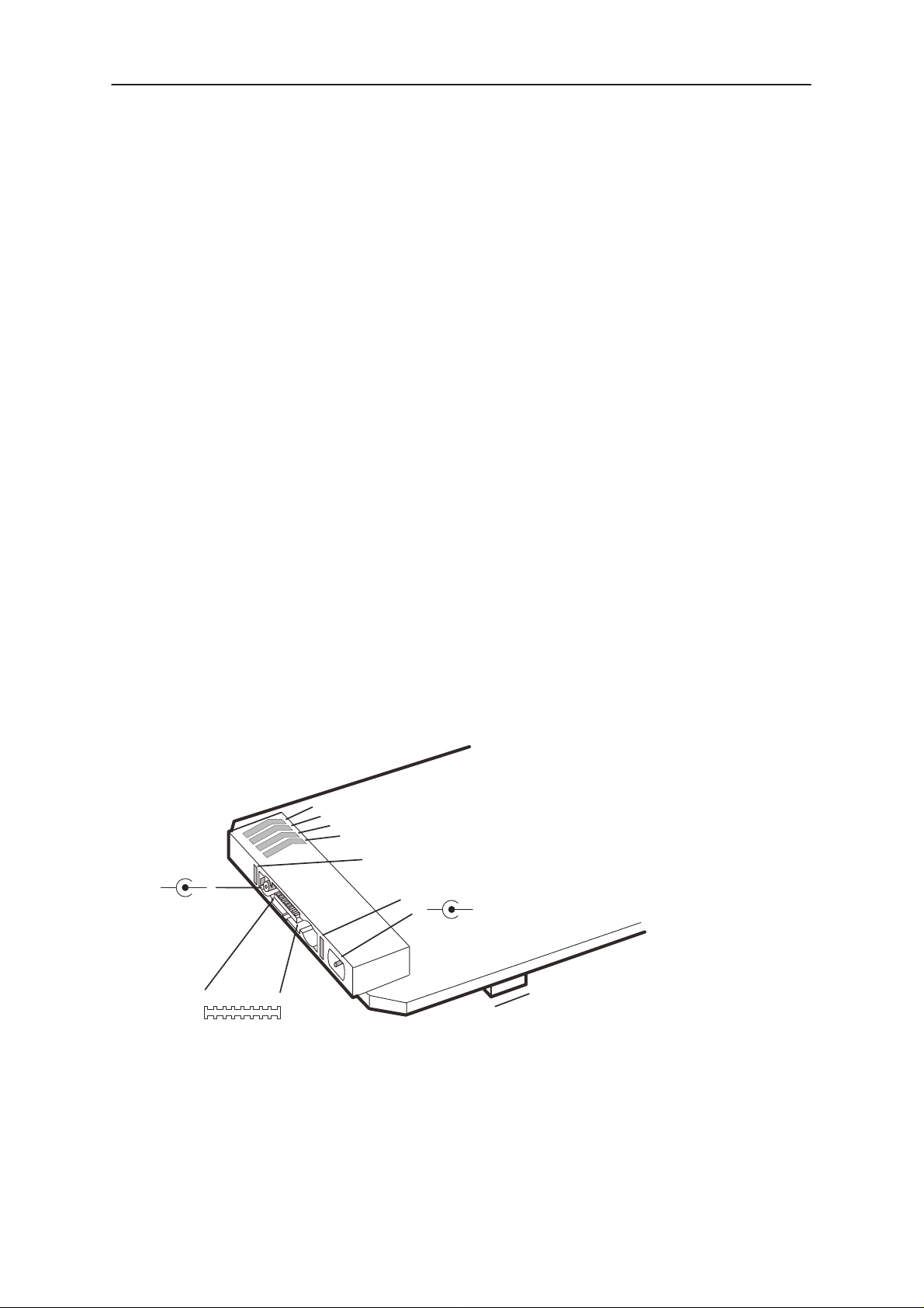
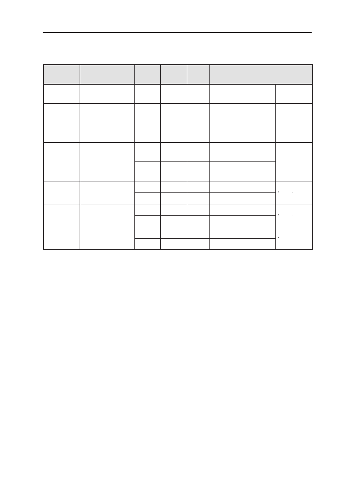
External and Internal Connectors
The system module has two connector, external bottom connector and
internal UIF module connector.
Bottom Connector X120
4
Battery connector
3
2
X120
1
4
Charging connector
3
2
Antenna
connector
2
1
16
System connector
9
18
1
1
21
X130
UIF module connector
D0000323
Page 1 – 4
Original 49/96
After Sales
THF–9
Technical Documentation
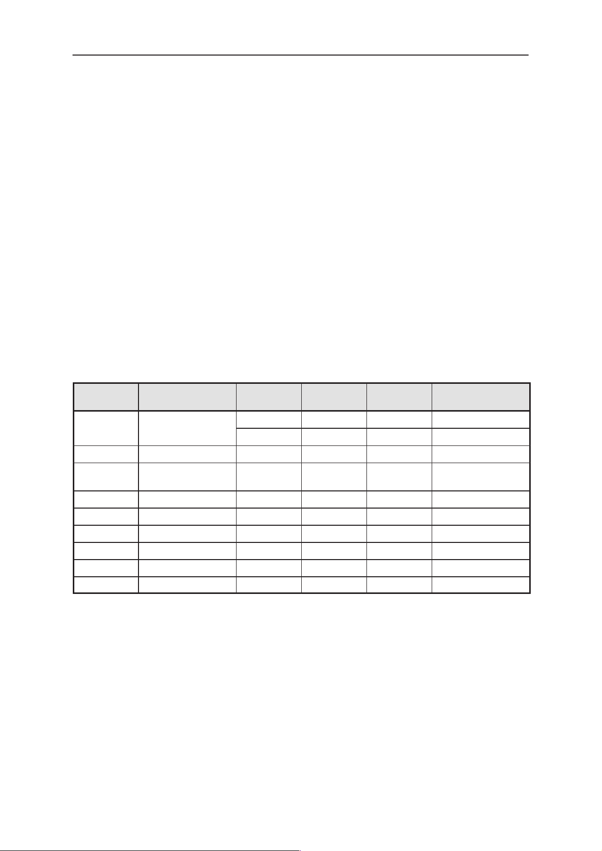
System Connector
Signal Name Pin Notes
GND 1, 3, 9 Power supply ground.
XMIC 2 External audio input from accessories
or handsfree microphone. There is a
pulldown resistor to turn the booster
on.
M2BUS 5 Serial bidirectional data and control be-
tween the handphone and accessories.
A 10k pull–up resistor in HP.
HOOK 6 HOOK–indication. The phone has a
100k pull–up resistor.
PHFS 7 Hands–free device power on/off.
XEAR 10 External audio output to accessories
or handsfree speaker.
There is a 100k pull–down to turn on
the junction box.
RF Block
BGND BGND Battery connector
BTEMP BTEMP Battery connector, Battery temperature
BSI BSI Battery connector
VBAT B+ Battery connector
VCS 8,16,CH+,
DC+
RFOUT RFOUT To duplex filter
RF RF From antenna
RFGND RFGND Ground for antenna
Battery charging voltage
Original 49/96
Page 1 – 5
THF–9
After Sales
RF Block
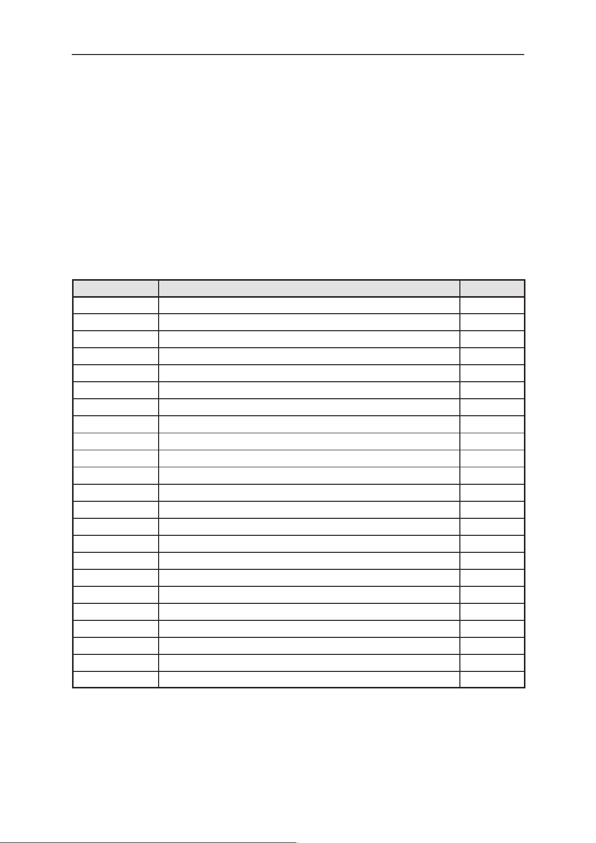
UIF connector X130
Signal Name Pin Notes
VL3 1 Logic supply voltage 4.75V
GND 2, 29 Ground
VBAT 3, 30 Battery voltage
LIGHTS 4 Backlights on/off
UIF(0:3) 5 – 8 Parallel data for LCD driver
UIF(4:5) 9 – 10 Lines for keyboard read and LCD con-
troller data
LCD_RW 9 LCD Driver read/write selection input
LCD_RS 10 LCD Driver register selection input
XLCDEN 11 LCD Driver chip select
ROW2 12 Line for keyboard read
Technical Documentation
XPWROFF 13 Power off control
COL(0:3) 13 – 16 Lines for keyboard write
CALL_LED 17 Call led enable
MICP 18 Microphone (positive node)
MICN 19 Microphone (negative node)
EARP 20 Earpiece (positive node)
EARN 21 Earpiece (negative node)
BUZZER 22 Buzzer control
XPWRON 23 Power on control from keyboard
ROW0 24 Line for keyboard read
LCDCLK 25 Clock signal for display
ROW1 26 Line for keyboard read
ROW3 27 Line for keyboard read
Page 1 – 6
Original 49/96
After Sales
bits/s
HP
ing con
THF–9
Technical Documentation
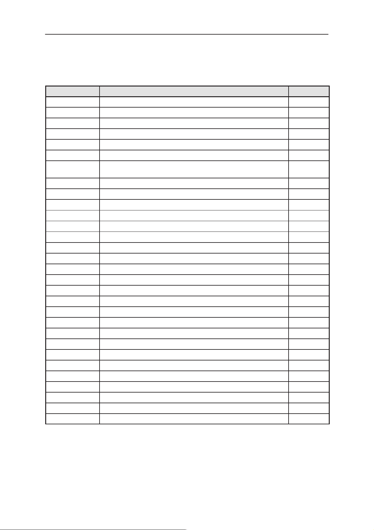
Control Signals
Pin /
Conn.
5/system M2BUS
6/system HOOK
7/system PHFS
Line Symbol Min Typ /
Max Description
Nom
0V 0.7V Input low level
2.3V 5.25VInput high level
0V 0.2V 0.35VOutput low level
4.1V 4.5V 5.0V Output high level
0V 0.7V Input low level
2.3V 3.5V Input high level
0V 0.2V 0.4V Output low, power
off
4.1V 4.5V 5.0V Output high, power
on
RF Block
Isink<5m
ABaud
rate 9600
.
Hook
HF device power on/off
8, 16/system
2/battery BSI
3/battery BTEMP 1.0V A 15k NTC between BTEMP
4/UIF LIGHTS
9–10/UIF UIF(4:5)
VCS
11V 12V 13V Isink < 730mA
730mA800mA870mAUin < 11V
503m
V
1.19V 1100mAh NiCd
1.65 V 1500mAh NiMH
0V 0.4V Output low, back-
2.8V 3.3V Output high, back-
0V 0.7V Input low
2.3V 3.6V Input high
500mAh NiMH
and ground in battery pack.
A 33k pull–up resistor in HP.
Vibrator control output (AC–
controlled)
lights off
lights on
A 100k
pull–up
resistor in
.
Backlight–
trol for
keymat
Keypad
input
5–11/UIF
12/UIF ROW2
Original 49/96
0V 0.4V Output low
2.3V 3.3V Output high
0V 0.7V Input low
2.8V 3.3V Input high
Output
for LCD
Keypad
input
Page 1 – 7
THF–9
After Sales
RF Block
MinLine SymbolPin /
Conn.
13–16/UIFCOL(0:3) 0V 0.7V Output low Keypad
17/UIF CALL_LED
22/UIF BUZZER
24/UIF ROW0
26/UIF ROW1
0V 0.4V Output low, call led
2.8V 3.3V Output high, call
0V 0.4V Output low, buzzer
2.8V 3.3V Output high, buzz-
0V 0.7V Input low
2.8V 3.3V Input high
0V 0.7V Input low
2.8V 3.3V Input high
Nom
off
led on
on
er off
Technical Documentation
DescriptionMaxTyp /
output
Keypad
input
Keypad
input
27/UIF ROW3
0V 0.7V Input low
2.8V 3.3V Input high
Keypad
input
Page 1 – 8
Original 49/96

After Sales
THF–9
Technical Documentation
Baseband Module
Introduction
Baseband module controls the internal operation of the phone. It controls the
user interface, i.e. LCD driver, keyboard and audio interface functions. The
module performs all signalling towards the system and carries out audio–frequency signal processing. In addition, it controls the operation of the transceiver and stores tuning data for the phone.
Technical Summary
All functional blocks of the baseband are mounted on a single multi layer
printed circuit board. This board contains also RF–parts. The chassis of the
radio unit contains separating walls for baseband and RF. All components
of the baseband are surface mountable. They are soldered using reflow . The
connections to accessories are fed through the bottom connector of the radio unit. The connections to User Interface –module (UIF) are fed through
a board to board connector . There is no physical connector between RF and
baseband.
RF Block
List of submodules
CTRLU Control Unit for the phone
PWRU Power supply
AUDIO Audio
RX Receiver
TX Transmitter
SYNT Synthesizer
These blocks are only functional blocks and therefore have no type nor
material codes.
Technical Specifications
Modes of Operation
The module has three operating modes: stand–by ,listening and the conversation mode.
Standby mode:
CPU‘s clock is switched off, only NIPA timer is running to take care battery save timings.
If charger is connected CPU‘s clock doesn‘t go to standby mode.
Original 49/96
Page 1 – 9
THF–9
After Sales
RF Block
Listening mode:
In the listening mode some blocks of the audio IC (NIPA) are in standby
state.
Conversation mode:
In the conversation mode all ICs are active.
Maximum Ratings
Operating ambient temperature range: –25 ... +55 °C.
Storage temperature range: –40 ... +85 °C.
VBAT max. 8.6 V (TX off) 7.5 V (TX on)
VCS max. 11.6 V.
Charging of the batteries is possible only in temperature range +5 ... +45 °C.
Technical Documentation
DC Characteristics
Pin / Conn. Line Symbol Minimum Typical /
Nominal
VCS
VBA T 5.3V 6.0V 8.8V
VRF 5.3V 6.0V 8.8V VBAT for RF mod-
VA 3.2V 3.3V 3.42V Imax = 40mA
VL 3.2V 3.3V 3.42V Imax = 20mA
VL2 3.2V 3.3V 3.42 Imax = 20mA
VL3 4.5V 4.75V 5.0V Imax = 180mA
VL4 3.8V 4.1V 4.6V Imax = 40mA
VREF 3.2V 3.3V 3.42V Imax = 5mA
11.0V 12.0V 13.0V chargers
730mA 800mA 870mA
Maximum Unit / Notes
ule
Page 1 – 10
Original 49/96
After Sales
THF–9
Technical Documentation
RF Block
CTRLU
Introduction
The Control block controls all phones functions and it includes modem
and SIS–processor too.
Technical Specifications
CTRLU Internal Signals, Inputs
Signal Description From
VL2 Logic supply voltage, 3.3V. PWRU
VL3 Logic supply voltage, 4.75V. PWRU
VL4 Supply voltage for SIS processor. PWRU
VREF Reference voltage 3.3V 3%. Max. PWRU
XRES Reset line from MUUMI PWRU
PWRON Power on signal from MUUMI PWRU
VCHARG Charger voltage to A/D converter PWRU
VBATSW Battery voltage to A/D converter. VCHARG
CLKMCU Clock signal from NIP A. AUDIO
NMI No maskable Interrupt reques from NIPA AUDIO
XINT Interrupt reques from NIPA. AUDIO
HOOK HOOK–indication SYSTEM
BTEMP Battery temperature SYSTEM
BSI Battery size indication SYSTEM
M2BUS Serial interface SYSTEM
RFTEMP RF temperature SYNT
RSSI Received signal strenght indication RX
TXI Transmitter output power level indication TX
XPWRON Power buttom from UIF. UIF
ROW0 Line for keyboard read. UIF
ROW1 Line for keyboard read. UIF
ROW2 Line for keyboard read. UIF
ROW3 Line for keyboard read. UIF
Original 49/96
Page 1 – 11
THF–9
After Sales
RF Block
Technical Documentation
CTRLU Internal Signals, Outputs
Signal Name Notes To
CSW Charger control PWRU
PHFS Hands–free device power on/off SYSTEM
M2BUS Common serial clock (nipa,sis) SYSTEM
AGC Gain control RX
RXE RX Circuit power on/off RX
SCLK Synchronous data clock for synthesizers SYNT
SDAT Synchronous data for synthesizers /
TX duplex filter current control 2 (option)
SLE Synthesizer data latch enable SYNT
TXE Transmitter control (on/off) TX
TXC Transmitter Power Control TX
XNCS NIPA chip select signal AUDIO
SYNT, TX
XNWR NIPA write control signal AUDIO
XNRD NIPA read control signal AUDIO
NA0–3 NIPA address bus AUDIO
ND0–7 NIPA data bus AUDIO
EARENA Ear amplifier enable AUDIO
KBINT Keyboard interrupt AUDIO
MBUSINT MBUS interrupt AUDIO
MBUSOUT MBUS out PWRU
LIGHTS Backlights on/of f UIF
COL0–3 Lines for keyboard read UIF
UIF0 Parallel data for LCD Driver UIF
UIF1 Parallel data for LCD Driver UIF
UIF2 Parallel data for LCD Driver UIF
UIF3 Parallel data for LCD Driver UIF
UIF4 / LCD_RW Line for keyboard read / LCD Driver rewd/write selection input UIF
UIF5 / LCD_RS Line for keyboard read / LCD Driver register selection input UIF
UIF6 / XLCDEN LCD Driver chip select UIF
CALL_LED Call led control UIF
Page 1 – 12
UIF
Original 49/96

After Sales
THF–9
Technical Documentation
Block Description
CTRLU – PWRU
MCU controls the watchdog timer in MUUMI. It sends a positive pulse at approximately 1 s to XPWROFF pin of the MUUMI
to keep the power on. If CTRLU fails to deliver this pulse, the
MUUMI will remove power from the system. CTRLU controls
also the charger on/off switching in the PWRU block. When
power off is requested CTRLU leaves MUUMI watchdog without reset. After the watchdog has elapsed MUUMI cuts off the
supply voltages from the phone. Battery charging is controlled
by CSW line.
VBATSW, Battery voltage measurement
Battery voltage can be measured from 5.4 V to 10.3 V nominal with 3.3 V reference voltage. The absolute accuracy is low
because of the reference 3 % accuracy and A/D–converter +/–
8 LSB accuracy. This battery voltage measurement offset error
must be calibrated with input voltage 6.0 V. The A/D conversion result can be calculated from equation:
RF Block
A/D readout = 1024 * (VBATSW* ( 47/147)) / VREF VREF=3.3 V
For example:
6.0 V results 595 = 253H
5.6 V results 556 = 22CH
VCHARG, Charger voltage measurement
Charger voltage can be measured up to 21.6 V nominal. The
A/D–conversion result can be calculated from equation :
A/D readout = 1024 * (VCSW*(15/115)) / VREF VREF=3.3 V
For example:
12.0 V gives 486 = 1E6H
6.0 V gives 243 = 0F3H
BSI, Battery size indication
Battery capacity can be defined with BSI resistor value calculated from equation:
BSI = 47k / ((4 mAh * 1023)/ C ) –1)
A/D–readout gives battery capacity from equation:
Original 49/96
A/D readout = C/3 C= Battery capacity
BTEMP, Battery temperature measurement
Battery temperature measurement is implemented with 15
kohm NTC and 33 kohm pull–up resistor. The A/D conversion
readout can be calculated from equation:
Page 1 – 13

THF–9
After Sales
RF Block
A/D readout= 1024* ( R
For example:
Battery voltage is measured over the VBATSW and charging
voltage over the VCHARG. Battery temperature is measured
over the BTEMP line. Battery size is determined by reading the
BSI line. This is pulled to +3,3V by 100kohm. In the battery
pack a ”size” resistor is connected between BSI and GND. Battery charging is controlled by CSW line. Battery charging is
controlled by CSW line.
CTRLU – AUDIO
Interface between micro–controller and NIPA circuit is bi–directional 8–bit data bus with 4 address lines. Address, data and
control lines are used in micro–controller as I/O–port pins. Data
lines direction must be controlled with micro–controller data
direction register. Interface includes address outputs NA0–3,
data inputs (read) / outputs (write) ND0–7, chip select control
output XCS , read control output XRD, write control output
XWR and interrupt input XINT. If NIPA circuit is not selected ,
control signals XRD and XCS must be in ’0’ state and address
output NA0–3 and NWR in ’1’ state and data lines ND0–7 must
be inputs .
Technical Documentation
NTC
/( R
NTC
+33k))
45 C gives 175 = 0AFH
25 C gives 320 = 140H
5 C gives 539 = 21BH
0 C gives 601 = 259H
CTRLU – UIF
Keyboard is connected directly to the controller. COL0–3 are
output lines and ROW0–3 and UIF4–5 are input lines. Also
watchdog is updated same time with keyboard scanning
(XPWROFF). Keyboard scanning is done by driving one COL
to 0 V at the time. If any key is pressed, then ROW of UIF(4:5)
goes to 0 V and phone knows which key is pressed.
Data to LCD Driver is written by UIF(0;3) (PDA0..PDA3) signals. UIF5 (LCD_RS) is instruction / data register selection line
and UIF6 (XLCDEN) is LCD drivers enable. UIF4 (LCD_RW) is
read / write selection line. New byte can written, when BUSY
flag is ”0” (it is not busy) from UIF3 and UIF5 (LCD_RS) = ”0”
and UIF4 (LCD_RW) = ”1” status.
Keyboards and LCD lights are controlled by LIGHTS signal.
UIF consist MIC,EAR, and BUZZER too
CTRLU – RX
RX circuit power is connected on/off by RXE signal.
Received signal strength is measured over the RSSI and inter-
mediate frequency is measured over the IF.
Page 1 – 14
Original 49/96

After Sales
THF–9
Technical Documentation
CTRLU – SYNT
RF temperature is measured over the RFTEMP. Frequency is
controlled by AFC signal. Synthesizer is controlled via synchronous serial bus SDAT/SCLK. The data is latched to the synthesizer by the positive edge of SLE line. TX synthesizer power
on/off (TXS/port P3) line is controlled via PLL circuit.
CTRLU – TX
Transmitter output power level is measured over the TXI. TXE
line activates power module. The power is controlled via TXC
line which is PWM–controlled output port.
Main Components
Hitachi H8/3093
H8/3093 is a CMOS micro–controller. All memory needed (192 kB ROM,
4 kB RAM) except the EEPROM, is located in the controller. MCU operating clock (=3.6864 MHz) is generated on NIPA.
RF Block
Controller Ports
Pin No Port Signal Description
1 PB0 SISCLK Clock for SIS prosessor
2 PB1 SISDATA Serialdata to SIS prosessor
3 PB2 EDATA Serial data to EEPROM
4 PB3 RXD Serial interface (M2BUS)
5 PB4 SCLK Serial clock for synthesiz
6 PB5 PHFS HF power on/off
7 PB6 PWRON Power button
8 PB7 SLE RX/TX synthesizer latch
9 P90 TXD Serial interface (M2BUS)
10 P92 RXD M2BUS net free timer input
11 P94 ECLK Clock to EEPROM
12 Vss GND Ground for processor.
13–20 P30–P37 ND0–7 Paraller data bus for NIPA
21 Vcc VL2 Power supply for processor
22 P10 NA0 Address line for nipa
23 P11 NA1 Address line for nipa
24 P12 NA2 Address line for nipa
25 P13 NA3 Address line for nipa
Original 49/96
Page 1 – 15

THF–9
After Sales
RF Block
26
27 P15 XNWR Read/write control to NIPA
28 P16 XNRD Read/write control to NIPA
29 P17 LIGHTS Backlight control
30 GND Ground for processor
31–34 P20–23 UIF0...3 /
35 P24 UIF4 /
36 P25 UIF5 /
37 P26 UIF6 /
38 P27 CALLCNT Call continue during battery change
P14 XNCS NIPA chip select
Keypad input /
PDA0...3
LCD_RW
LCD_RS
XLCDEN
Paralled data for LCD
LCD Driver read/write selection
Keypad input / LCD Driver register
selection
LCD driver chip select
Technical Documentation
P40–P47
39–42 P50–P53 COL0–3 Keypad outputs
43 P60
44 MD0
45 MD1
46
47 STBY
48 RES XRES Reset from MUUMI
49 NMI NMI Interrupt request from NIPA
50 Vss GND Ground
51 EXTAL EXTAL External system clock from NIPA
52 XTAL
53 Vcc VL2
54 P63 TXE Transmitter on/off
55 P64 AGC Gain control
56 P65 RXE RX circuit power on/off
57 RESO
58 AVcc
59 P70 VBATSW Battery voltage
60 P71 VCHARG Charger voltage
61 P72 RSSI Received signal strength
62 P73 TXI Transmitter power monitor
63 P74 BTEMP Battery temperature
Page 1 – 16
Original 49/96

After Sales
THF–9
Technical Documentation
64
P75 BSI Battery size indication
RF Block
65 P76 RFTEMP RF temperature
66 P77 HOOK Hook indicator
67 Vref Vref Reference voltage for processor
68 AVcc Vref Reference voltage for processor
69 P80 XINT Interrupt request from NIPA
70 P81 EARENA Speaker amplifier enable
71 P82 CALL_LED Indicates a call
72 P83 VIBRA Vibra control
73 PA0 ROW0 Keypad input
74 PA1 ROW1 Keypad input
75 PA2 ROW2 Keypad input
76 PA3 ROW3 Keypad input
77 PA4 CSW Charging control
78 PA5 SDAT Serial data for synthesiser
79 PA6 TXC TX syntetisizer enable. Active high.
80 PA7
68HC11A8
68HC11A8 is a SIS (subscriber identification) circuit connected to the controller over serial bus IIC.
Pin Description
EXTAL Clock input from nipa
RESET Reset input
PD0 IIC bus data
PD1 IIC bus clock
EEPROM
There is one 8k EEPROM in phone. EEPROM is a nonvolatile memory into
which is stored the tuning data for the phone. In addition, it contains the
short code memory locations to retain user selectable phone numbers.
Pin Description
SDA IIC bus data
SCL IIC bus clock
Original 49/96
Page 1 – 17

THF–9
After Sales
RF Block
Technical Documentation
PWRU
Introduction
The power block provides the supply voltages for the baseband, and includes also the charging electronics.
Technical Specifications
PWRU Internal Signals, Inputs
Signal Description From
CSW Charger control CTRLU
MBUSOUT Serial interface CTRLU
XPWRON Power on control from keyboard UIF
XPWROFF Power off control from controller (watch dog) CTRLU
VBAT Battery voltage input SYSTEM
VCS Charging supply voltage from charger SYSTEM
PWRU Internal Signals, Outputs
Signal Description To
XRES Master reset CTRLU, AU-
DIO
PWRON Power on signal for microprosessor. CTRLU
VL Logic supply voltage, 3.3V AUDIO
VL2 Logic supply voltage, 3.3V CTRLU
VL3 Logic supply voltage, 4.75V CTRLU, AU-
DIO, UIF
VL4 SIS processor supply voltage, 4.1V CTRLU
VA Analog supply voltage. Max 40 mA. SYNT,AU-
DIO
VREF Reference voltage 3.3V 3%. Max. 5mA. CTRLU, RF,
TX
VBATSW Battery voltage to A/D converter. CTRLU
VCHARG Charger voltage to A/D converter. CTRLU
Page 1 – 18
Original 49/96

After Sales
THF–9
Technical Documentation
Block Description
The baseband power supplying circuit includes:
– the supply voltages:
VL 0.5mA for NIPAs digital circuits
VL2 40mA for digital circuits
VL3 20mA for LCD
VL4 20mA for SIS–processor
VA 20mA for analog circuits
VREF 5mA reference voltage for A/D–converters and
– Regulator has been used before MUUMI
– switched output of battery (VBATSW) and charger voltage (VCHARG)
measurements to MCU A/D–converter
– battery voltage detection and reset logic
– charger switch control output used to limit battery voltage VBAT < 8.8V
– power on/off switch input (XPWRON), buffered output to MCU
(PWRON)
– watchdog timer using oscillator in COFF pin , cleared by falling edge
input in PWROFFX, elapsing time for watchdog timer is 3 ... 4 seconds
– M2BUS open drain output driver is not used.
RF Block
regulators
The charge switch driving circuit is implemented with discrete components. This circuit includes transient voltage protection, soft charge
switching, low voltage battery charging and battery disconnecting with
charger connected protection. This circuit also limits battery voltage when
charger is connected to protect MUUMI and TX transistors.
Power circuitry have three different operating modes: POWER OFF , RESET and POWER ON. In POWER OFF state MUUMI regulator outputs
are disabled and reset control output signal (PURX) is active low.
MUUMI internal oscillator at pin COFF is working in all operating modes.
MUUMI goes through short RESET state (100ms ) to POWER ON–state
, if PWR–button is pressed or charger voltage input is connected to
charging input VCS (charging voltage detection in MUUMI input VCHAR
is level active). In RESET–state regulator outputs VL,VA and VREF are
active and PURX–signal is active low. If battery voltage on MUMMIs pin
is lower than 4.1 V (3.9V...4.3V) the circuit cannot go to POWER ON
state. MUUMI goes also to RESET state, when battery voltage on MUUMIs pin is falling below 3.9 V (3.7V...4.1V). This situation is possible, when
battery is fully discharged or battery is disconnected.
In POWER ON mode all regulator outputs are active and MUUMI reset
signal output PURX is inactive high. Micro–controller XPWROFF–output
signal clears at falling edge the watchdog inside MUUMI. If the watchdog
is not cleared , MUUMI goes to POWER OFF state. When the charger is
connected and battery voltage on MUUMIs pin is higher than 4.1V, module stays in POWER ON mode.
Original 49/96
Page 1 – 19

THF–9
After Sales
RF Block
Technical Documentation
The micro–controller controls battery charging with CSW output (which is
PWM–controlled output port) and MUUMI limits the maximum battery voltage to 8.8 V with CHRGSW–output.
No current flows from charger (VCHARG) to battery, if MCU output CSW
is active low and XRES signal is inactive high. The battery is charged
also, when charger is connected and XRES signal is active low. The
charging circuit charges the battery during RESET to higher than 5.3 V.
The charging electronics is controlled by the CTRLU. When the charging
voltage is applied to the phone while the phone is powered up, the
CTRLU detects it and starts controlling the charging.
If the phone is in power–off, the MUUMI will detect the charging voltage. If
the battery voltage is high enough the reset will be released and the
CTRLU will start controlling the charging. If the battery voltage is too low
the phone is in reset and charging control circuitry will pass the charging
current to the battery. When the battery voltage on MUUMIs pin has
reached 4.1V (3.9...4.3V) the reset will be removed and the CTRLU
starts controlling the charging. This all is invisible to the user.
V116 is the charging switch; it is governed by the controller (CSW line) via
voltage regulator V114 and V115. In fast charge mode CSW is ”1” and in
maintain charge mode there is controller controlled pulses. In charge off
state CSW is ”0”. In maintain charge mode pulse ratio depends of charger
and temperature.
There is three different ways to switch power on:
– Power key pressing grounds the XPWRON line. The MUUMI defects
that and switches the power on.
– Charger detection on MUUMI detects that charger is connected and
switches power on.
– MUUMI will switch power on when the battery is connected. If the bat-
tery is changed during the call, the power is kept on. If not the power
is switched off.
Page 1 – 20
Original 49/96

After Sales
THF–9
Technical Documentation
Block Diagram of MUUMI
VBAT1
1
22
VBAT2
VBAT3
5
M2BUSIN
11
760k
PWM
15
760k
CHARGER
CTRL
LOGIC
BANDGAP
REF
70k
40k
VBATSW
M2BUSOUT
VREF
RF Block
17
12
VL
23
VA
2
4
VCHAR
21
VBAT
13
14
3
PWRONX
PWROFFX
TEST
32k
760k
760k
Main Components
– MUUMI asic
CHRGSW
PURX
10
LOW VBAT
& CHARGER
DETECT
PWR ON/OFF
&
RESET LOGIC
Creset
20
16
Coff
VL_ENA
VA_ENA
VREF_ENA
VSW_ENA
VCHAR
GND1
24
GND2
19
GND3
7
PWRONXBUFF
VCHARSW
Cref
6
18
Makes the voltages, has power switch, charger and battery
detection
and watchdog.
8
9
– transistor V116 and diode V118
– regulators N130 and N140
Original 49/96
The charging current is passed through these components.
N130 decreases battery voltage to 4.75 V which is suitable for
MUUMI asic. N140 makes the supply voltage VL3 (4.75 V) to
display and logic circuits.
Page 1 – 21

THF–9
After Sales
RF Block
Audio
Introduction
The block includes NIPA audio/signalling processor in a 64 TQFP package for NMT450 and NMT900 systems.
Main features
– Single chip FFSK modem and audio circuit
– Full duplex 1200 baud signalling
– DMS facility
– Low power consumption modes
– Programmable output clocks with clock stop for MCU and LCD
– 8 bit parallel interface with pull ups
– FSK indicator and level detector
– Speech volume indicator
– Programmable timer
– IF counter
– 8 bit DAC
– FII filter and gain control
– Low noise microphone amplifier
– Input for a handset microphone or an accessory
– Microphone sensitivity compensation +4.8/–4.2 dB range (4 bits)
– Compander
– RX and TX filters
– Tx hard limiter
– Tx AGC
– Internal reference compensation +1.00/–0.75 dB range(3 bits)
– Summing stage for voice/data, signalling and fii
– Transmitter compensation amplifier with +3.75/–3.75 dB range (4 bits)
– Receiver compensation amplifier with +3.75/–3.75 dB range (4 bits)
– Volume control amplifier with –20/+17.5 range (4 bits)
– Earphone amplifier with drive capability for ceramic earpiece
– Buffered output for a handset or an accessory
– Mute switches
– Dual and single tone multi–frequency generator
– Driver for buzzer amplifier
– Hands free functions
Technical Documentation
Page 1 – 22
Original 49/96

After Sales
THF–9
Technical Documentation
RF Block
Technical Specifications
Audio Internal Signals, Inputs
Signal Description From
VL Logic supply voltage, 3.3V PWRU
VA Analog supply voltage, 3.3V PWRU
VL3 Logic supply voltage, 4.75V PWRU
XRES Reset line from MUUMI PWRU
XNRD Read control signal CTRLU
XNCS Chip select signal CTRLU
XNWR Write control signal CTRLU
NA0...A3 4–bit address bus CTRLU
ND0...D7 8–bit bidirectional data bus CTRLU
EARENA Earphone amplifier enable CTRLU
KBINT Keyboard interrupt CTRLU
MBUSINT MBUS interrupt CTRLU
DAF Detected audio signal from receiver RX
IF (2nd) Intermediate frequency for AFC function RX
XMIC External audio input from accessories SYSTEM
MICP Microphone (positive node) UIF
MICN Microphone (negative node) UIF
Audio Internal Signals, Outputs
Signal Description To
XEAR External audio output to accessories SYSTEM
MOD Audio output to synthesizer SYNT
AFC VCTCXO control SYNT
BUZZER Buzzer signal UIF
EARP Earpiece (positive node) UIF
EARN Earpiece (negative node) UIF
LCDCLK Clock signal for LCD driver UIF
CLKMCU Clock signal for MCU CTRLU
XINT Interrupt reques to MCU CTRLU
NMI No maskable Interrupt reques to MCU CTRLU
Original 49/96
Page 1 – 23
THF–9
After Sales
RF Block
Technical Documentation
Pin list of NIPA
Pin no Symbol Pin type Description
1 VDD1 + 3.3 V Supply voltage, digital
2 XRD DIN/pd Read control signal, active state LOW, pull–down > 50
k
3 XCS DIN/pd Chip select signal, active state LOW, pull–down > 50
k
4 A3 DIN/pu 4–bit address bus, MSB, pull–up > 50 k
5 A2 DIN/pu 4–bit address bus, pull–up > 50 k
6 A1 DIN/pu 4–bit address bus, pull–up > 50 k
7 A0 DIN/pu 4–bit address bus, LSB, pull–up > 50 k
8 D7 DIO 8–bit bidirectional data bus MSB
9 D6 DIO 8–bit bidirectional data bus
10 D5 DIO 8–bit bidirectional data bus
11 D4 DIO 8–bit bidirectional data bus
12 D3 DIO 8–bit bidirectional data bus
13 D2 DIO 8–bit bidirectional data bus
14 D1 DIO 8–bit bidirectional data bus
15 D0 DIO 8–bit bidirectional data bus LSB
16 VDD2 + 3.3 V Supply voltage, digital
17 NMI DOUT Non maskable Interrupt request
18 XCLR DIN HW reset input, active state LOW
19 TMODE DIN/pd Test mode selection, pull–down > 50 k
20 TSEL DIN/pd Test select, pull–down > 50 k
21 XINT DOUT Interrupt request to MCU, active state LOW
22 MBUSINT DIN MBUS interrupt request, falling edge active
23 KBINT DIN Keyboard interrupt request, falling edge active
24 IF AIN IF input
25 VSS2 0 V Supply voltage, digital ground
26 VSA2 0 V Supply voltage, analog ground
27 DAF AIN Signal input
28 FILO AOUT Rxfilter output
29 EXPI AIN Expander input
30 EAMPBO AOUT Expander Amplifier B output
31 EWCI AIN Expander Window Comparator input
32 EXPO AOUT Expander output
33 VDA2 + 3.3 V Supply voltage, analog
34 VOLI AIN Volume control ampl. input (Volume)
Page 1 – 24
Original 49/96

After Sales
THF–9
Technical Documentation
DescriptionPin typeSymbolPin no
35 EXTEAR AOUT Buffered output for handset or an accessory
36 EVGND AIN Earphone driver virtual ground
37 EARM AOUT Earphone driver output
38 EARP AOUT Earphone driver output
39 CWCI AIN Compressor window comparator input
40 DACO AOUT DA converter output
41 SIDEAR AOUT Sidetone output
42 REF AIN Internal analog signal ground 1.65 V
43 MIC AIN Microphone amplifier input
44 BIMIC AOUT Microphone bias current output
45 CMIC AIN Microphone current stabilization capacitor
46 EXTMIC AIN Audio input for a handset or an accessory
47 TXBPO AOUT Transmit bandpass filter output
RF Block
48 VDA1 + 3.3 V Supply voltage, analog
49 COMI AIN Compressor input
50 COMO AOUT Compressor output
51 EMPI AIN Pre emphasis input
52 FIIOUT AOUT Received FII signal
53 TOUT DOUT Test output, digital
54 ATST AOUT Audio Filter Test output
55 MOD AOUT Transmit path output
56 VSA1 0 V Supply voltage, analog ground
57 VSS1 0 V Supply voltage, digital ground
58 BUZZ DOUT Buzzer output
59 ATOUT AOUT Test pin
60 CLKOUT COUT (7.3728 MHz) 3.6864 MHz crystal oscillator output
61 CLKIN CIN (7.3728 MHz) 3.6864 MHz crystal oscillator input or
input for the external clock
62 CLKLCD DOUT Clock signal for LCD, 230.4 kHz or 57.6 kHz
63 CLKMCU DOUT Clock signal for MCU, 3.6864 MHz or 7.3728 MHz
64 XWR DIN/pu Write control signal, active state LOW, pull–up > 50
k
Original 49/96
Page 1 – 25

THF–9
After Sales
RF Block
Block Description
ATST
ATOUT
LIM
VOL
AGC
SUM
TXTRI
TXAAF
EMPI
CWCI
COMI COMO
TXBPO
SINGEN
PREEMP
RXAAF
MODTRFIL
MODRXFIL
DATACOMP
TXLP TXTRI+TXPOSTFIL
AGC
PREEM LIM
COMPR
txbpo
aloop (to RXMUX)
SINGEN MODTRFIL
TRSTBY
RFLAG
TFLAG
(to SIDEAR)
FSKMOD
TR
CTRL
RECCTRL
INTERNAL
CLOCKS
WPOSFIL
WTRFIL
SUM
TRREG
STATUS
BITS
RECREG
DPLL
MOD
BUZZ
BUZZ
ddtmf
SMUX
DFLAG
AFC
loop (to MODRXFIL)
MODTRPOST
XBSSBY
XTALKSBY
XBUZZSBY
XIFSBY
XDTMFSBY
DRIV
CONTROL BITS
CREG
TIMER
DETFIL
DETED
DACO
D/A
8 bit
XDACSBY
INTERFACE
FIIBUF
A0 A1 A2 A3 D0 D1 D2 D3 D4 D5 D6 D7
NMI
XINT
XWR
XRD
XCS
Technical Documentation
FIIOUT
EAR
FIIPOST
EARP
HF
EARM
CONTR
EVGND
RXATT ACC
EXP VOL
DEEMP+RXFIL
EXTEAR
SIDEAR
SIDEAR
txbpo
(from TXBP)
EXPO
EAMPBO
FILO
64 pins
VOLI
EWCI
EXPI
MICAM
Page 1 – 26
TXMUX+TXAAF TXATT MICTRI TXBP
MIC
CMIC
BIMIC
ddtmf (to BUZZDRIV)
DTMFCOMP
dtmf
DTMF GEN
EXTMIC
CLKLCD CLKMCU
XCLR
TMODE
(to RXMUX)
REF GEN
CLKIN
CLOCKDIV
TSEL
OSC
IFAMP
CLKOUT
IFCNTR
IF
FSKIND
GND GEN
REF
FSKDIS
DATACOMP
KBINT
MBUSINT
MODRXFIL
LEVEL
FSKLEV
VDD2
VDD1
FIIFIL(4kHz)+FIITRI
dtmf
loop (from WPOSFIL)
VSS2
VSA1
VDA1
VDA2
RXMUX+AAFIL
VSA2
VSS1
aloop (from TXPOSTFIL)
RXTRI RXAAF
DAF
Original 49/96

After Sales
THF–9
Technical Documentation
Transmit (TX) Audio Signal Path
The TX audio signal is processed in the NIPA circuit and fed via the MOD
line to the TX synthesizer on SYNTHESIZER module.
NIPA ASIC contains the following stages for TX signal processing:
MICAM:
The signal from the microphone is fed to this stage and amplified up to 200 mVrms.
TXMUX + TXAAF:
TX source selection (exmic/mic/dmmf/muted). Txaafil prevents
aliasing in TXBP filter.
TXATT:
TXATT is a hands free attenuator. Maximum attenuation is selectable from four levels: –30, –27, –24 or –21 dB.
RF Block
MICTRI:
MICTRI is for different microphone (phone microphone, headset and handset etc.) sensitivity compensation. It is used also
for dtmf level setting. Gain 16 levels, step 0.6 dB.
BANDPASS:
Tx bandpass filter takes out high freq noise and low freq hum.
COMPR:
It compresses speech dynamic area to avoid noise at tx and
radio path. It is a amplitude compressor and ratio is 2:1 in dB
scale. It can be bypassed for measurement
or dtmf purposes.
PREEMP:
Pre–emphasis filter gives +6 dB/oct emphasis.
AGC:
Soft limiter is needed in order to suppress inter–modulation.
Signal measuring circuitry measures peak–to–peak voltage. If
signal on soft limiter input is not a sine signal (clipped in preceding stages), peak–to–peak signal level is increased in the
post limiter filter.
LIM:
TXLP:
Original 49/96
Hard limiter. It cuts the signal transients to 1131 mVpp levels.
The corner frequency of tx lowpass filter is 3400 Hz. Amplitude
attenuation is 12 dB/oct after the corner point. Filter includes
notch at 4 kHz.
Page 1 – 27

THF–9
After Sales
RF Block
Technical Documentation
TXTRI:
TXTRI is for nominal deviation tuning. Gain 8 levels, step 0.5
dB.
TXPOSTFIL:
Postfil eliminates filter clock.
SUM:
Speech, data and FII signals are summed together.
WTRFIL:
This block is a lowpass filter for FII and data. Transmitter Compensation Amplifier is these too. Gain 16 levels, step 0.5 dB.
WPOSFIL:
WPOSFIL filters out the replicates of the output spectrum
around WTRFIL clock frequency and its harmonics.
Receive (RX) Audio Signal Path
NIPA contains the following stages for RX signal processing:
RXTRI:
RXTRI is for demodulation sensitivity compensation. Gain 16
levels, step 0.5 dB.
RXAAF:
RX aafilter filters out noise and other high frequency components from the incoming signal. It prevents aliasing in FIIFIL,
RXFIL and MODRXFIL.
RXMUX+AAFIL:
Rxmux selects speech from DAF–pin or DTMF from generator
or a loop from TXTRI or mute. Aafil prevents aliasing in RXFIL.
DEEMP+ RXFIL:
Rx filter filters out high freq noise and low freq hum. It has de–
emphasis –6 dB/oct for the received speech signal. Design
should include notch at 4kHz.
EXP:
VOL:
Page 1 – 28
It expands speech dynamic back to normal. It is a amplitude
expander and ratio is 1:2 in dB scale. It can be bypassed for
measurement or dtmf purposes.
VOL is for earphone or accessory speaker/earphone volume
control. Volume Control Amplifier. Gain 16 levels over –20 to
+17.5 dB in 2.5 dB steps.
Original 49/96

After Sales
THF–9
Technical Documentation
RXATT:
RXATT is a hands free attenuator. Maximum attenuation is selectable from four levels: –30, –27, –24 or –21 dB. Hands free
controller (HF CONTR) measures peak–to–peak level of the
received audio and controls gains of the transmit and receive
attenuators as a function of measured signal level.
EAR:
The Earphone Amplifier is a single input, differential output amplifier for a ceramic earpiece.
ACC:
Buffer for accessory line is capable of driving high capacitive
load. Gain and response of the buffer are fixed.
Transmitting data path
The data to be transmitted will be loaded into the transmitting register
TRREG. From the TRREG register the 8 bit data is transformed to serial
data which is sent to the FSK modulator (FSKMOD) and sine wave generator (SINGEN) and then to the summing block (SUM).
RF Block
Receiving data path
The data from anti alias filter is connected through the modems RX filter
(MODRXFIL) to the data comparator (DA TACOMP) and then to FSK discriminator. Further from FSK discriminator data is connected to detecting filter
(DETFIL) and from there to digital phase locked loop (DPLL).
IF
Intermediate frequency counter (IFCTR) is on the modem to measure
the frequency of IF signal.
AFC
AFC makes the synthesizer fine tuning. It can be used for channel sidestep also.
AFC DA–converter output DC level tunes RF oscillator (VCXO) .
FII path
The FII signal is filtered and amplified with a 4 kHz bandpass filter (FIIFIL). FIITRI is for FII sensitivity compensation. The filtered FII is then fed to
summing block (SUM).
Buzzer driver
Buzzer driver is a PWM output, so volume of buzzer is controlled by length
of the pulse.
Original 49/96
Page 1 – 29

THF–9
After Sales
RF Block
Technical Documentation
Clock driver
Clock divider generates internal clock frequencies by dividing master
clock frequency which is created by an internal crystal oscillator and an
external 3.6864 MHz crystal. Buffered crystal frequency is obtained at pin
CLKMCU and clock for LCD–driver at pin CLKLCD (f= 230.4 kHz).
Earphone amplifier
NIPA can drive ceramic earphone only. Because of used dynamic earphone in THF–9, it need power amplifier for earphone. Main components
of amplifier are transistors V751, V753 ,V754, V755 and diode V752.
Page 1 – 30
Original 49/96

After Sales
THF–9
Technical Documentation
RF Module
Introduction
RF block is designed for a handportable phone, which operates in NMT450
systems. Purpose of the RF module is to receive and demodulate radio frequency signal from the base station and to transmit a modulated RF signal
to the base station. RF parts are designed to work as specified in NMT450
specification for handportable phone.
List of Functional Blocks
Receiver (RX)
Transmitter (TX)
Two UHF–synthesizer
All functional blocks of the RF are mounted on a single multilayer printed circuit board. This board contains also CPU. Chassis of the radio unit contains
separating walls for RF sub–blocks. All components of the RF except TX–
power module and duplexer are SMD type.
RF Block
Technical Specifications
Modes of Operation
Standby Mode
Radio unit is ready for reception. RX–synthesizer and receiver are operat-
ing, other RF circuits are powered down. When battery save is active, all
RF circuits are powered down except TX power detection.
Conversation Mode
Analog receiver section operating, TX–synthesizer, modulator and trans-
mitter power amplifier are powered up.
Control Signals and RF/System Block Interface
Signal Description
AFC VCTCXO control voltage
Factory tuned value
AGC Gain control
DAF Detected audio and base station data
IF 2nd intermediate frequency for automatic freq. con-
trolling
MOD Modulation line for voice and data
Original 49/96
Page 1 – 31

THF–9
After Sales
RF Block
Technical Documentation
Signal Description
RFTEMP RF temperature, which is detected by NTC
RSSI Received Signal Strength Indicator
RXE RX circuit power on/off
SCLK Synthesizer clock pulse
SDAT Synthesizer serial data
SLE Synthesizer enable
TXE Transmitter enable, switches VBAT supply voltage
for TX
circuits
TXI Transmitter power indicator
TXC Analog control voltage for TX power level setting
TXS/synthesizer TX synthesizer enable, control is set by SDAT via
PLL
port P3 circuit
VCCR Supply voltage for RF
VBAT Supply voltage for TX power module
VRF Supply voltage for RF regulator
VREF Reference voltage for RX regulator and for TX pow-
er
control loop
VRXVCO RX VCO supply voltage
Software Compensation Algorithms
RSSI vs. Temperature and Channel
Received Signal Strength Indicator values will be compensated for different
temperatures and channels by software. RSSI values are calibrated at the
room temperature for different channels. The affect of temperature are corrected by temperature factor.
Receiver Automatic Gain Control (AGC)
Automatic Gain Control increases receiver linearity at high input signal
levels. AGC will be set on, when received signal level is more than –30
dBm and off, when received signal level is lower than –40 dBm.
Page 1 – 32
Original 49/96

After Sales
THF–9
Technical Documentation
Current Consumption
RF operation mode Current consumption (mA)
Standby, battery save off 42 mA
Standby, battery save on 0.25 mA
Transmission, full power (1 W) 850 mA
Transmission, low power (150 mW) 430 mA
Note! Current values are valid for 6.0 V battery voltage.
Functional Description
Receiver
Receiver can be divided to RX amplifier, RX filter, 1st mixer, 1st IF1–amplifier, IF1–filter, IF1–buffer, FM IF amplifier and detector circuit and regulator. Special care has been used to minimize current consumption.
RF Block
Standby Mode, when Battery Save is off
Received antenna signal RX is fed via duplexer to RF–amplifier. After 17
dB amplification signal is fed via RX–filter (SAW) to 1st mixer input. RX–
VCO generates injection frequency RXINJ, which is applied to 1st mixer.
RXINJ signal is 45 MHz below receiving frequency. 1st IF 45 MHz (RX–
RXINJ) is generated in the mixer, amplified in 1st IF1–amplifier and fed to
6–pole filter.
After the filter there is IF1 buffer, which stabilizes the impedances between filter and Sony CXA1343N circuit. In this IC the signal is mixed
down to the 2nd IF 450 kHz. Limiting amplifiers and detector operate on
this frequency. Demodulated signal is further fed to modem via DAF–line.
CXA1343N produces also RSSI–voltage, which is proportional to the received RF signal strength. IC is also fed with 3rd harmonic of the
VCTCXO frequency, which acts as an 44.55 MHz injection for 2nd mixer.
Regulator circuit V310...V312 provides supply voltage for receiver circuit
and for the RX– and TX–synthesizers.
Standby Mode, when Battery Save is on
In this operation mode all RF functions are set to sleep except TX power
detection. System block contains a timer, which defines the length of the
sleep. After battery save mode RF returns always to standby mode.
Original 49/96
Page 1 – 33

THF–9
After Sales
RF Block
Conversation Mode
Propagation of the received signal in the RX block is the same as described previously in the standby mode.
Synthesizers
LO–frequencies needed in the RF block are generated using two VCOs,
dual frequency synthesizer, 14.85 MHz VCTCXO and 3rd harmonic multiplier for VCTCXO frequency. VCTCXO acts as a reference frequency for
the PLL circuit. Frequency 44.55 MHz is used to 2nd LO frequency of the
receiver.
Synthesizer is controlled via serial bus SDAT. SCLK line has a clock signal for the synthesizer. The synthesizer enabling is done via SLE line. TX
synthesizer power on/off (TXS/port P3) line is controlled via PLL circuit.
Control information is programmed by using SDAT line.
Technical Documentation
Page 1 – 34
Original 49/96

After Sales
THF–9
Technical Documentation
Transmitter
Functional Description
Standby Modes
All transmitter circuits are switched off. Only the TX power
detection is active.
Conversation Mode
Modulating audio signal is fed via MOD line to TX–VCO. VCO’s
output signal is at the TX band. The output signal is buffered
before TX power module. After the TX power module signal is
fed via duplex filter and mechanical antenna switch to the antenna.
Synthesizer port P3 (TXS) line is used to activate TX–VCO and
its buffer. TXE line activates power module. Desired transmitting power level is set by TXC–voltage, which includes the
compensation information for the shape of the duplexer insertion loss.
RF Block
Original 49/96
Page 1 – 35

THF–9
After Sales
RF Block
Technical Documentation
This page intentionally left blank.
Page 1 – 36
Original 49/96
 Loading...